EP3916759A1 - Plaquette et son procédé de fabrication, et dispositif à semi-conducteur - Google Patents
Plaquette et son procédé de fabrication, et dispositif à semi-conducteur Download PDFInfo
- Publication number
- EP3916759A1 EP3916759A1 EP20832551.4A EP20832551A EP3916759A1 EP 3916759 A1 EP3916759 A1 EP 3916759A1 EP 20832551 A EP20832551 A EP 20832551A EP 3916759 A1 EP3916759 A1 EP 3916759A1
- Authority
- EP
- European Patent Office
- Prior art keywords
- silicon
- dicing
- vias
- wafer
- scribe lane
- Prior art date
- Legal status (The legal status is an assumption and is not a legal conclusion. Google has not performed a legal analysis and makes no representation as to the accuracy of the status listed.)
- Granted
Links
Images




Classifications
-
- H—ELECTRICITY
- H10—SEMICONDUCTOR DEVICES; ELECTRIC SOLID-STATE DEVICES NOT OTHERWISE PROVIDED FOR
- H10W—GENERIC PACKAGES, INTERCONNECTIONS, CONNECTORS OR OTHER CONSTRUCTIONAL DETAILS OF DEVICES COVERED BY CLASS H10
- H10W42/00—Arrangements for protection of devices
- H10W42/121—Arrangements for protection of devices protecting against mechanical damage
-
- H—ELECTRICITY
- H10—SEMICONDUCTOR DEVICES; ELECTRIC SOLID-STATE DEVICES NOT OTHERWISE PROVIDED FOR
- H10P—GENERIC PROCESSES OR APPARATUS FOR THE MANUFACTURE OR TREATMENT OF DEVICES COVERED BY CLASS H10
- H10P52/00—Grinding, lapping or polishing of wafers, substrates or parts of devices
-
- H—ELECTRICITY
- H10—SEMICONDUCTOR DEVICES; ELECTRIC SOLID-STATE DEVICES NOT OTHERWISE PROVIDED FOR
- H10P—GENERIC PROCESSES OR APPARATUS FOR THE MANUFACTURE OR TREATMENT OF DEVICES COVERED BY CLASS H10
- H10P14/00—Formation of materials, e.g. in the shape of layers or pillars
- H10P14/40—Formation of materials, e.g. in the shape of layers or pillars of conductive or resistive materials
- H10P14/412—Deposition of metallic or metal-silicide materials
-
- H—ELECTRICITY
- H10—SEMICONDUCTOR DEVICES; ELECTRIC SOLID-STATE DEVICES NOT OTHERWISE PROVIDED FOR
- H10P—GENERIC PROCESSES OR APPARATUS FOR THE MANUFACTURE OR TREATMENT OF DEVICES COVERED BY CLASS H10
- H10P50/00—Etching of wafers, substrates or parts of devices
- H10P50/20—Dry etching; Plasma etching; Reactive-ion etching
- H10P50/24—Dry etching; Plasma etching; Reactive-ion etching of semiconductor materials
- H10P50/242—Dry etching; Plasma etching; Reactive-ion etching of semiconductor materials of Group IV materials
-
- H—ELECTRICITY
- H10—SEMICONDUCTOR DEVICES; ELECTRIC SOLID-STATE DEVICES NOT OTHERWISE PROVIDED FOR
- H10P—GENERIC PROCESSES OR APPARATUS FOR THE MANUFACTURE OR TREATMENT OF DEVICES COVERED BY CLASS H10
- H10P50/00—Etching of wafers, substrates or parts of devices
- H10P50/60—Wet etching
- H10P50/64—Wet etching of semiconductor materials
- H10P50/642—Chemical etching
-
- H—ELECTRICITY
- H10—SEMICONDUCTOR DEVICES; ELECTRIC SOLID-STATE DEVICES NOT OTHERWISE PROVIDED FOR
- H10P—GENERIC PROCESSES OR APPARATUS FOR THE MANUFACTURE OR TREATMENT OF DEVICES COVERED BY CLASS H10
- H10P54/00—Cutting or separating of wafers, substrates or parts of devices
-
- H—ELECTRICITY
- H10—SEMICONDUCTOR DEVICES; ELECTRIC SOLID-STATE DEVICES NOT OTHERWISE PROVIDED FOR
- H10W—GENERIC PACKAGES, INTERCONNECTIONS, CONNECTORS OR OTHER CONSTRUCTIONAL DETAILS OF DEVICES COVERED BY CLASS H10
- H10W20/00—Interconnections in chips, wafers or substrates
- H10W20/20—Interconnections within wafers or substrates, e.g. through-silicon vias [TSV]
-
- H—ELECTRICITY
- H10—SEMICONDUCTOR DEVICES; ELECTRIC SOLID-STATE DEVICES NOT OTHERWISE PROVIDED FOR
- H10W—GENERIC PACKAGES, INTERCONNECTIONS, CONNECTORS OR OTHER CONSTRUCTIONAL DETAILS OF DEVICES COVERED BY CLASS H10
- H10W74/00—Encapsulations, e.g. protective coatings
- H10W74/01—Manufacture or treatment
-
- H—ELECTRICITY
- H10—SEMICONDUCTOR DEVICES; ELECTRIC SOLID-STATE DEVICES NOT OTHERWISE PROVIDED FOR
- H10W—GENERIC PACKAGES, INTERCONNECTIONS, CONNECTORS OR OTHER CONSTRUCTIONAL DETAILS OF DEVICES COVERED BY CLASS H10
- H10W74/00—Encapsulations, e.g. protective coatings
- H10W74/10—Encapsulations, e.g. protective coatings characterised by their shape or disposition
- H10W74/131—Encapsulations, e.g. protective coatings characterised by their shape or disposition the semiconductor body being only partially enclosed
- H10W74/134—Encapsulations, e.g. protective coatings characterised by their shape or disposition the semiconductor body being only partially enclosed the encapsulations being in grooves in the semiconductor body
-
- H—ELECTRICITY
- H10—SEMICONDUCTOR DEVICES; ELECTRIC SOLID-STATE DEVICES NOT OTHERWISE PROVIDED FOR
- H10W—GENERIC PACKAGES, INTERCONNECTIONS, CONNECTORS OR OTHER CONSTRUCTIONAL DETAILS OF DEVICES COVERED BY CLASS H10
- H10W90/00—Package configurations
-
- H—ELECTRICITY
- H10—SEMICONDUCTOR DEVICES; ELECTRIC SOLID-STATE DEVICES NOT OTHERWISE PROVIDED FOR
- H10W—GENERIC PACKAGES, INTERCONNECTIONS, CONNECTORS OR OTHER CONSTRUCTIONAL DETAILS OF DEVICES COVERED BY CLASS H10
- H10W74/00—Encapsulations, e.g. protective coatings
- H10W74/40—Encapsulations, e.g. protective coatings characterised by their materials
- H10W74/43—Encapsulations, e.g. protective coatings characterised by their materials comprising oxides, nitrides or carbides, e.g. ceramics or glasses
-
- H—ELECTRICITY
- H10—SEMICONDUCTOR DEVICES; ELECTRIC SOLID-STATE DEVICES NOT OTHERWISE PROVIDED FOR
- H10W—GENERIC PACKAGES, INTERCONNECTIONS, CONNECTORS OR OTHER CONSTRUCTIONAL DETAILS OF DEVICES COVERED BY CLASS H10
- H10W74/00—Encapsulations, e.g. protective coatings
- H10W74/40—Encapsulations, e.g. protective coatings characterised by their materials
- H10W74/47—Encapsulations, e.g. protective coatings characterised by their materials comprising organic materials, e.g. plastics or resins
-
- H—ELECTRICITY
- H10—SEMICONDUCTOR DEVICES; ELECTRIC SOLID-STATE DEVICES NOT OTHERWISE PROVIDED FOR
- H10W—GENERIC PACKAGES, INTERCONNECTIONS, CONNECTORS OR OTHER CONSTRUCTIONAL DETAILS OF DEVICES COVERED BY CLASS H10
- H10W74/00—Encapsulations, e.g. protective coatings
- H10W74/40—Encapsulations, e.g. protective coatings characterised by their materials
- H10W74/47—Encapsulations, e.g. protective coatings characterised by their materials comprising organic materials, e.g. plastics or resins
- H10W74/476—Organic materials comprising silicon
Definitions
- the present disclosure relates to the field of semiconductor technology, and in particular to a wafer, a manufacturing method thereof, and a semiconductor device.
- a multi-stacked wafer includes die areas and a dicing area.
- the die areas may be damaged due to stress from dicing the scribe areas.
- relatively large dicing areas are applied currently.
- the large dicing area results in a reduction in the effective utilization of the wafer and thus an increase in chip cost.
- the present disclosure provides a wafer, a manufacturing method thereof, and a semiconductor device, thereby at least to some extent overcoming one or more problems caused by the limitations and defects of related techniques.
- a wafer manufacturing method which includes: providing a wafer body on which provided with a scribe lane for dicing; forming dicing through-silicon-vias at the scribe lane to form a dicing line, wherein the dicing through-silicon-vias are filled with a protective material.
- said forming the dicing through-silicon-vias at the scribe lane comprises the steps of: forming blind vias at the scribe lane from a first surface of the wafer body; filling the protective material into the blind vias; and thinning the wafer body from a second surface opposite to the first surface until the blind vias are exposed.
- said forming the dicing through-silicon-vias at the scribe lane comprises the steps of: forming first dicing through-silicon-vias at a scribe lane of a first wafer body; filling the protective material into the first dicing through-silicon-vias; forming second dicing through-silicon-vias at a scribe lane of a second wafer body at positions aligned with the first dicing through-silicon-vias, wherein the first wafer body and the second wafer body are stacked; and filling the protective material into the second dicing through-silicon-vias.
- the dicing through-silicon-vias comprise continuously distributed or separately distributed through-silicon-vias.
- two or more rows of the dicing through-silicon-vias are formed at the scribe lane.
- a width of the dicing through-silicon-vias is in a range from 2 microns to 20 microns, and a depth of the dicing through-silicon-vias is in a range from 15 microns to 150 microns.
- the protective material comprises one or more selected from copper, tungsten, aluminum, tantalum, titanium, tantalum nitride, titanium nitride, silicon oxide, silicon nitride, silicon oxynitride, silicon carbide, silicon carbonitride, polyimide and tetraethyl orthosilicate.
- an air gap is provided in one of the dicing through-silicon-vias.
- a wafer which includes: a wafer body, on which provided a scribe lane for dicing; dicing through-silicon-vias provided at the scribe lane, wherein the dicing through-silicon-vias are filled with a protective material.
- the dicing through-silicon-vias are formed at the scribe lane along an extension direction of the scribe lane.
- the dicing through-silicon-vias comprise continuously distributed or separately distributed through-silicon-vias.
- two or more rows of the dicing through-silicon-vias are formed at the scribe lane.
- a width of the dicing through-silicon-vias is in a range from 2 microns to 50 microns, and a depth of the dicing through-silicon-vias is in a range from 15 microns to 150 microns.
- the protective material comprises one or more selected from copper, tungsten, aluminum, tantalum, titanium, tantalum nitride, titanium nitride, silicon oxide, silicon nitride, silicon oxynitride, silicon carbide, silicon carbonitride, polyimide and tetraethyl orthosilicate.
- an air gap is provided in one of the dicing through-silicon-vias.
- a semiconductor device which includes two or more layers of the above said wafers, in which the two or more layers of the wafers are stacked.
- the following list shows the reference numerals in the figures: 100, wafer body; 110, die; 120, scribe lane; 200, dicing through-silicon-via; 210, blind via; 230, first dicing through-silicon-via; 240, second dicing through-silicon-via; 250, air gap; 20, protective material layer; 300, first wafer body; 400, second wafer body.
- the terms “one”, “a”, “the”, “said” and “at least one” are used to indicate the presence of one or more elements/components/etc.
- the terms “include/including” and “have/having” are used to indicate open-ended inclusive, and mean that in addition to the listed elements/components/etc., there may be other elements/components/etc.
- the terms “first”, “second” and “third” are only used as a label, not a limit to the number of objects.
- the wafer manufacturing method may include the following steps:
- the dicing through-silicon-vias 200 that are filled with the protective material at the scribe lane 120 to pre-dicing the wafer, the damage of the die region 110 caused by the dicing stress is prevented during wafer dicing.
- the dicing through-silicon-via 200 can effectively reduce the width of the scribe lane 120 and facilitate miniaturization of the scribe lane 120, thereby improving the effective wafer utilization.
- the wafer body 100 may be divided into the scribe lanes 120 and the die areas 110, and during dicing, a dicing knife acts on the scribe lanes 120, while the die regions 110 are untouched.
- the wafer body 100 may include a silicon based substrate such as a silicon epitaxial wafer, silicon-on-insulator, etc., or a substrate of other semiconductor material such as GaN, and the substrate may be an intrinsic semiconductor substrate, or N-type doped or P-type doped semiconductor substrate, which is not specifically limited in the present disclosure.
- a dielectric layer may be provided on the substrate, and the material of the dielectric layer may be one or more of silicon oxide, silicon nitride, or silicon oxynitride.
- the dielectric layer may be formed by a method such as chemical vapor deposition, atomic layer deposition, or the like, in specific examples. It is understood that the dielectric layer may be f one layer of insulating material, or may be stacked layers of the same or different insulating materials.
- step S120 may include the following steps as shown in FIG. 2 :
- the blind vias 210 are formed at the scribe lane 120 from the first surface of the wafer body 100.
- the blind vias 210 may be formed by dry etching, wet etching, laser etching, or dry and wet combined etching.
- the dry etching may be reactive ion etching or inductively coupled plasma etching
- the wet etching may use hydrofluoric acid solution, hydrofluoric acid buffered etching solution, potassium hydroxide solution, or TMAH solution.
- the blind vias 210 are located at the scribe lane 120 having the cross section of a rectangular or trapezoidal shape.
- the positions of the blind vias 210 can be defined by a photoresist, which can be coated on the first side of the wafer body 100, exposed with a corresponding photomask to transfer the pattern of the photomask to the photoresist, and developed such that the photoresist layer exposes the regions where the dicing through-silicon-vias 200 are to be formed ; and the blind vias 210 are formed by etching.
- a protective material may be filled in the blind via 210.
- the protective material may be one or more of conductive materials such as copper, tungsten, aluminum, tantalum, titanium, tantalum nitride, titanium nitride and the like.
- an insulating layer may be deposited on the first surface of the wafer body 100 and on the inside walls of the blind via 210.
- the insulating layer can be formed by chemical vapor deposition, physical vapor deposition, or thermal growth.
- the above-mentioned conductive material then fills in the blind via 210, by electroplating, for example.
- a seed layer is first deposited on the insulating layer, and a metal protective layer is electroplated on the seed layer.
- a metal layer is also formed on the first surface of the wafer body 100, which needs to be removed by such as etching or chemical mechanical polishing.
- the filling material is one or more of silicon oxide, silicon nitride, silicon oxynitride, silicon carbide, silicon carbonitride, polyimide, and tetraethyl orthosilicate
- it may be filled with a process of chemical vapor deposition or physical vapor deposition or thermal growth.
- a protective material layer 20 is also formed on the first surface of the wafer body 100, shown in FIG. 8 .
- the protective material layer 20 can be removed or not removed according to actual needs. Further, an air gap 250 may be formed inside the protective material filled in the blind via 210.
- step S230 as shown in FIG. 9 , the second surface of the wafer body 100 is thinned until the blind vias 210 are exposed.
- the second surface of the wafer body 100 which is opposite to the first surface may be thinned by etching or chemical mechanical polishing.
- the first surface of the wafer body 100 may be the front side of the wafer body 100, and the second side is the back side of the wafer body 100.
- step S120 may include:
- the first dicing through-silicon-vias 230 may be formed at the scribe line 120 on the first wafer body 300.
- the process is rather complicated in which blind vias 210 may be firstly formed on each of the wafer bodies, then the wafer bodies 100 are thinned after filling the vias with the protective material and lastly bonded together to form the multiple layers of stacked wafers. Therefore, a process may be adopted, in which a two-wafer stack structure is formed first, and then dicing through-silicon-vias are formed on each of the wafer bodies 100. This process can simplify the manufacturing process and improve the production efficiency.
- the two-wafer stack structure includes the first wafer body 300 and the second wafer body 400 that are stacked together.
- the first dicing through-silicon-vias 230 may be formed on the first wafer body 300 to expose the second wafer 400.
- the first dicing through-silicon-vias 230 are filled with a protective material.
- second dicing through-silicon-vias 240 which respectively align exactly to the first crack-stopping through-silicon-vias 230, may be formed on the surface of the second wafer body 400 to expose the first dicing through-silicon-vias 230.
- the second dicing through-silicon-vias 240 are filled with the protective material. This process eliminates the thinning step, therefore it simplifies the manufacturing process.
- the first dicing through-silicon-vias 230 may be formed by dry etching, wet etching, laser etching, or combined dry and wet etching.
- the dry etching may be the reactive ion etching or the inductively coupled plasma etching
- the wet etching may be etching with hydrofluoric acid solution, hydrofluoric acid buffered etching solution, potassium hydroxide solution, or TMAH solution.
- the first dicing through-silicon-vias 230 are located at the scribe lane 120 having the cross section of rectangular or trapezoidal shape.
- the position of the first dicing through-silicon-vias 230 can be defined by a photoresist, which is coated on the surface of the first wafer body 300, exposed with a corresponding mask to transfers the pattern of the mask to the photoresist layer; and developed to expose the regions where the first dicing through-silicon-vias 200 are to be formed; and the first dicing through-silicon-vias 230 are then formed by etching.
- a protective material may be filled in the first dicing through-silicon-via 230.
- the protective material may be one or more of the conductive materials such as copper, tungsten, aluminum, tantalum, titanium, tantalum nitride, and titanium nitride.
- a layer of insulating material may be formed on the walls of the first dicing through-silicon-vias 230 and on the surface of the wafer body 100 as well.
- the insulating layer may be formed, for example, by chemical vapor deposition, physical vapor deposition or thermal growth.
- the above-mentioned conductive material may be filled in the first dicing through-silicon-vias 230, for example, by electroplating.
- a seed layer is deposited on the surface of the insulating layer, then a metal protective layer is electroplated on the seed layer.
- the metal layer is also formed on the surface of the wafer body 100, and the metal layer needs to be removed, for example, by etching or chemical mechanical polishing.
- the filling material is one or more of silicon oxide, silicon nitride, silicon oxynitride, silicon carbide, silicon carbonitride, polyimide, and tetraethyl orthosilicate
- it may be filled in by such as chemical vapor deposition, physical vapor deposition or thermal growth.
- a protective material layer 20 is also formed on the surface of the first wafer body 300.
- the protective material layer 20 may be removed or may not be removed according to actual needs.
- an air gap 250 may be formed within the protective material filled in the first dicing through-silicon-via 230.
- the second dicing through-silicon-vias 240 respectively aligning to the first crack-stopping through-silicon-vias 230 may be formed at the scribe lane 120 on the second wafer body 400.
- the second dicing through-silicon-vias 240 may be formed by dry etching, wet etching, laser etching, or dry and wet combined etching.
- the dry etching may be the reactive ion etching or the inductively coupled plasma etching
- the wet etching may be etching with a potassium hydroxide solution.
- the second dicing through-silicon-vias 240 are located at the scribe line 120, and the cross-section of the second dicing through-silicon-vias 240 may be rectangular or trapezoidal.
- the position of the second dicing through-silicon-vias 240 can be defined by a photoresist which is coated on the surface of the second wafer body 400, exposed with a corresponding photomask to transfer the pattern of the mask to the photoresist layer, and developed to expose the regions where the second dicing through-silicon-vias 240 are to be formed; and the second dicing through-silicon-vias 240 are formed by etching.
- the second dicing through-silicon-vias 240 are filled with the protective material.
- the protective material may be one or more of the conductive materials such as copper, tungsten, aluminum, tantalum, titanium, tantalum nitride, and titanium nitride.
- a layer of insulating material can be formed on the walls of the second dicing through-silicon-vias 240 and on the surface of the wafer body 100 as well.
- the insulating layer may be formed, for example, by chemical vapor deposition, physical vapor deposition or thermal growth.
- the above-mentioned conductive material may be filled in the second dicing through-silicon-vias 240, for example, by electroplating.
- a seed layer is deposited on the surface of the insulating layer, then a metal protective layer is electroplated on the seed layer.
- the metal layer is also formed on the surface of the wafer body 100, which needs to be removed, for example, by etching or chemical mechanical polishing.
- the filling material is one or more of silicon oxide, silicon nitride, silicon oxynitride, silicon carbide, silicon carbonitride, polyimide, and tetraethyl orthosilicate
- it may be filled in by such as chemical vapor deposition or physical vapor deposition or thermal growth are applied.
- a protective material layer 20 is also formed on the surface of the first wafer body 400.
- the protective material layer 20 may be removed or may not be removed according to actual needs.
- an air gap 250 may be formed within the protective material filled in the second dicing through-silicon-via 240.
- each additional stacked layer of wafer may be stacked first and then subject to forming the dicing through-silicon-vias. This method can simplify the manufacturing process and improve the production efficiency.
- the dicing through-silicon-vias 200 are formed at the scribe lane 120 along the extension direction of the scribe lane.
- the dicing through-silicon-vias 200 include continuously distributed dicing through-silicon-vias or separated distributed through-silicon-vias. Multiple rows of dicing through-silicon-vias 200 may be formed at the scribe lane 120.
- the width L of the dicing through-silicon-vias 200 ranges from 2 ⁇ m to 20 ⁇ m, and the depth S of the dicing through-silicon-vias 200 ranges from 15 ⁇ m to 150 ⁇ m.
- the width L of the entire area of the through-silicon-vias ranges from 2 ⁇ m to 20 ⁇ m.
- the width of the dicing through-silicon-vias 200 refers to the distance between the sidewalls of the dicing through-silicon-vias 200 parallel to the scribe line 120.
- multiple rows of dicing through-silicon-vias 200 may be formed in the scribe lane 120, and the multiple rows of dicing through-silicon-vias 200 may be arranged in parallel in the scribe lane 120. Multiple rows of dicing through-silicon-vias form multiple dicing lines which can further ease the dicing stress.
- the wafer manufacturing method provided by the examples of the present disclosure effectively prevented the damage of the die regions 110 caused by the dicing stress during wafer dicing, by providing the dicing through-silicon-vias 200, which are filled with the protective material and arranged at the scribe lane 120.
- the dicing through-silicon-vias 200 can effectively reduce the width of the scribe lane 120, facilitate the miniaturization of the scribe lane 120 and improve the resultant wafer utilization rate.
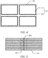
- This exemplary example also provides a wafer, as shown in FIG. 4 , which includes a wafer body 100 and dicing through-silicon-vias 200 in which the wafer body 100 is provided with a scribe lane for dicing. 120., and the dicing through-silicon-vias 200 are provided at the scribe lane 120 and filled with a protective material.
- the wafer provided by the example of the present disclosure prevents the damage on die regions 110 caused by the dicing stress during wafer dicing by the dicing through-silicon-vias 200 filled with protective material formed at the scribe lane 120.
- the dicing through-silicon-vias 200 can effectively reduce the width of the scribe lane 120, and facilitate the miniaturization of the scribe lane 120, thus, improves the effective utilization rate of the wafer.
- the wafer body 100 can be divided into a scribe lane 120 and a die region 110. During dicing, the dicing knife acts on the scribe lane 120 and the die region 110 is untouched.
- the wafer body 100 may be a silicon substrate including a silicon epitaxial layer, silicon on an insulator layer, etc., or a substrate of other semiconductor material such as GaN, or an intrinsic semiconductor substrate, or a N-type doped or P-type doped semiconductor substrate, which, however, is not limited to the above in the examples of the present disclosure.
- a dielectric layer may be disposed on the substrate. The material of the dielectric layer may be one or more of silicon oxide, silicon nitride, and silicon oxynitride.
- the dielectric layer may be formed by a method such as chemical vapor deposition, atomic layer deposition, and the like. It is understandable that the dielectric layer may be a single layer of insulating material, or may be multiple stacked layers of same or different insulating materials.
- the disclosed dicing through-silicon-vias 200 are formed at the scribe lane 120 along the extension direction of the scribe lane 120.
- the dicing through-silicon-vias 200 include continuously distributed through-silicon-vias or separately distributed through-silicon-vias. Multiple rows of dicing through-silicon-vias 200 are formed at the scribe lane 120.
- the width L of the dicing through-silicon-vias 200 ranges from 2 ⁇ m to 20 ⁇ m, and the depth S of the dicing through-silicon-vias 200 ranges from 15 ⁇ m to 150 ⁇ m.
- the total width L of the entire area of the dicing through-silicon-vias ranges from 2 ⁇ m to 20 ⁇ m.
- the width of the dicing through-silicon-vias 200 refers to the distance between the two sidewalls of the dicing through-silicon-vias 200 parallel to the scribe line 120.
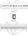
- the shape of the cross-section of the dicing through-silicon-vias may be rectangle as shown in FIG. 12 , or may be meshy, circular, elliptic or polygonal, etc. The disclosure does not limit the shape.
- the protective materials may include one or more of: copper, tungsten, aluminum, tantalum, titanium, tantalum nitride, titanium nitride, silicon oxide, silicon nitride, silicon oxynitride, silicon carbide, silicon carbon nitride, polyimide, and tetraethyl orthosilicate. Further, an air gap 250 is provided inside the dicing through-silicon-via 200.
- the dicing through-silicon-vias 200 may include an insulating layer and a protective material layer.
- the insulating layer is between the sidewalls of through-vias on the wafer body 100 and the protective material.
- an insulating layer may be formed firstly on the through-via sidewalls and the first surface of the wafer body 100.
- the insulating layer can be formed by such as chemical vapor deposition, physical vapor deposition or thermal growth.
- the above-mentioned conductive material is filled in the through-silicon-vias by such as electroplating. First a seed layer is deposited on the insulating layer, and a metal protective layer is electroplated on the seed layer.
- the filling material is one or more of silicon oxide, silicon nitride, silicon oxynitride, silicon carbide, silicon carbonitride, polyimide, and tetraethyl orthosilicate
- the it may be may be filled by chemical vapor deposition or physical vapor deposition or thermal growth.
- a protective material layer 20 is formed on the first surface of the wafer body 100.
- the protective material layer may be removed or may not be removed according to actual needs.
- an air gap 250 may be formed inside the protective material filled in the blind via 210.
- the wafer disclosed by the example is provided with the dicing through-silicon-vias 200 which are filled in with the protective material and disposed at the scribe lane 120, such that the die region 110 is protected from being damage by the dicing stress during wafer scribing.
- the dicing through-silicon-vias 200 can effectively reduce the width of the scribe lane 120, facilitate the miniaturization of the scribe lane 120, and improve the effective utilization rate of the wafer.
- This exemplary example also provides a semiconductor device, which includes multiple layers of aforementioned wafers which are stacked. There are dicing through-silicon-vias 200 at the scribe lane 120 in each of the stacked wafers. The positions of the dicing through-silicon-vias of the multiple layers of the wafers align to each other. After the multiple layers of the wafers are stacked, the dicing through-silicon-vias overlap in their projections on each of the wafers. As the stacked wafers are cut along the dicing through-silicon-vias 200, a plurality of stacked dies is obtained.
Landscapes
- Internal Circuitry In Semiconductor Integrated Circuit Devices (AREA)
- Chemical & Material Sciences (AREA)
- Chemical Kinetics & Catalysis (AREA)
- General Chemical & Material Sciences (AREA)
- Physics & Mathematics (AREA)
- Engineering & Computer Science (AREA)
- Plasma & Fusion (AREA)
Applications Claiming Priority (2)
| Application Number | Priority Date | Filing Date | Title |
|---|---|---|---|
| CN201910580407.9A CN112151368B (zh) | 2019-06-28 | 2019-06-28 | 晶圆及其制作方法、半导体器件 |
| PCT/CN2020/072497 WO2020258866A1 (fr) | 2019-06-28 | 2020-01-16 | Plaquette et son procédé de fabrication, et dispositif à semi-conducteur |
Publications (3)
| Publication Number | Publication Date |
|---|---|
| EP3916759A1 true EP3916759A1 (fr) | 2021-12-01 |
| EP3916759A4 EP3916759A4 (fr) | 2022-07-13 |
| EP3916759B1 EP3916759B1 (fr) | 2024-03-06 |
Family
ID=73892049
Family Applications (1)
| Application Number | Title | Priority Date | Filing Date |
|---|---|---|---|
| EP20832551.4A Active EP3916759B1 (fr) | 2019-06-28 | 2020-01-16 | Procédé de fabrication d'un dispositif à semi-conducteur |
Country Status (4)
| Country | Link |
|---|---|
| US (1) | US20230230936A1 (fr) |
| EP (1) | EP3916759B1 (fr) |
| CN (1) | CN112151368B (fr) |
| WO (1) | WO2020258866A1 (fr) |
Families Citing this family (5)
| Publication number | Priority date | Publication date | Assignee | Title |
|---|---|---|---|---|
| CN115985849A (zh) * | 2021-10-14 | 2023-04-18 | 中芯国际集成电路制造(北京)有限公司 | 一种堆叠晶圆结构及切片方法 |
| CN114446876B (zh) * | 2022-04-12 | 2022-07-01 | 湖北三维半导体集成创新中心有限责任公司 | 晶圆切割方法 |
| CN115223933B (zh) * | 2022-07-29 | 2025-04-25 | 豪威集成电路(成都)有限公司 | 半导体器件及其制作方法 |
| CN115376905B (zh) * | 2022-10-27 | 2023-01-31 | 山东中清智能科技股份有限公司 | 一种半导体晶片的切割工艺 |
| CN119297159B (zh) * | 2023-07-03 | 2026-04-03 | 长鑫存储技术有限公司 | 半导体结构及其制作方法、激光切割方法、半导体单元 |
Family Cites Families (23)
| Publication number | Priority date | Publication date | Assignee | Title |
|---|---|---|---|---|
| US5691248A (en) * | 1995-07-26 | 1997-11-25 | International Business Machines Corporation | Methods for precise definition of integrated circuit chip edges |
| TW407314B (en) * | 1999-08-30 | 2000-10-01 | Mosel Vitelic Inc | Method of lowering the stress for wafer sawing |
| US6838299B2 (en) * | 2001-11-28 | 2005-01-04 | Intel Corporation | Forming defect prevention trenches in dicing streets |
| KR100537892B1 (ko) * | 2003-08-26 | 2005-12-21 | 삼성전자주식회사 | 칩 스택 패키지와 그 제조 방법 |
| US7888236B2 (en) * | 2007-05-14 | 2011-02-15 | Taiwan Semiconductor Manufacturing Co., Ltd. | Semiconductor device and fabrication methods thereof |
| TW200921776A (en) * | 2007-11-09 | 2009-05-16 | Powertech Technology Inc | Wafer cutting method, die structure and its multi-die package method |
| CN101471320A (zh) * | 2007-12-27 | 2009-07-01 | 力成科技股份有限公司 | 基板封装结构 |
| KR101054492B1 (ko) * | 2009-08-06 | 2011-09-02 | 한국기계연구원 | 적층용 단위 칩의 제조방법과, 단위 칩을 이용한 3차원 적층 칩 및 그 제조방법 |
| JP5625558B2 (ja) * | 2010-02-22 | 2014-11-19 | サンケン電気株式会社 | 半導体ウェハ、及び半導体装置の製造方法 |
| TWI414047B (zh) * | 2010-03-17 | 2013-11-01 | 財團法人工業技術研究院 | 電子元件封裝結構及其製造方法 |
| US20130075892A1 (en) * | 2011-09-27 | 2013-03-28 | Taiwan Semiconductor Manufacturing Company, Ltd. | Method for Three Dimensional Integrated Circuit Fabrication |
| US8748297B2 (en) * | 2012-04-20 | 2014-06-10 | Infineon Technologies Ag | Methods of forming semiconductor devices by singulating a substrate by removing a dummy fill material |
| US8772126B2 (en) * | 2012-08-10 | 2014-07-08 | Infineon Technologies Ag | Method of manufacturing a semiconductor device including grinding from a back surface and semiconductor device |
| US20150069609A1 (en) * | 2013-09-12 | 2015-03-12 | International Business Machines Corporation | 3d chip crackstop |
| CN104752571A (zh) * | 2013-12-31 | 2015-07-01 | 晶能光电(江西)有限公司 | 一种晶圆级白光led芯片的切割方法 |
| JP2014112719A (ja) * | 2014-02-24 | 2014-06-19 | Lintec Corp | 半導体ウエハ |
| CN105720016B (zh) * | 2014-12-02 | 2019-08-02 | 日月光半导体制造股份有限公司 | 半导体衬底、半导体封装结构和其制造方法 |
| DE102015100783A1 (de) * | 2015-01-20 | 2016-07-21 | Infineon Technologies Ag | Verfahren zum Zertrennen eines Wafers und Halbleiterchip |
| US20170062399A1 (en) * | 2015-08-24 | 2017-03-02 | Globalfoundries Inc. | Method and structure for low-k face-to-face bonded wafer dicing |
| CN106299073B (zh) * | 2016-09-30 | 2019-02-19 | 映瑞光电科技(上海)有限公司 | 发光二极管晶圆及其形成方法 |
| US10319696B1 (en) * | 2018-05-10 | 2019-06-11 | Micron Technology, Inc. | Methods for fabricating 3D semiconductor device packages, resulting packages and systems incorporating such packages |
| WO2020024277A1 (fr) * | 2018-08-03 | 2020-02-06 | 深圳市为通博科技有限责任公司 | Procédé d'encapsulation de puce |
| CN210110749U (zh) * | 2019-06-28 | 2020-02-21 | 长鑫存储技术有限公司 | 晶圆及半导体器件 |
-
2019
- 2019-06-28 CN CN201910580407.9A patent/CN112151368B/zh active Active
-
2020
- 2020-01-16 US US17/040,954 patent/US20230230936A1/en active Pending
- 2020-01-16 WO PCT/CN2020/072497 patent/WO2020258866A1/fr not_active Ceased
- 2020-01-16 EP EP20832551.4A patent/EP3916759B1/fr active Active
Also Published As
| Publication number | Publication date |
|---|---|
| WO2020258866A1 (fr) | 2020-12-30 |
| CN112151368A (zh) | 2020-12-29 |
| EP3916759B1 (fr) | 2024-03-06 |
| CN112151368B (zh) | 2025-05-30 |
| EP3916759A4 (fr) | 2022-07-13 |
| US20230230936A1 (en) | 2023-07-20 |
Similar Documents
| Publication | Publication Date | Title |
|---|---|---|
| EP3916759B1 (fr) | Procédé de fabrication d'un dispositif à semi-conducteur | |
| US12119294B2 (en) | Through-substrate via structure and method of manufacture | |
| US11069647B2 (en) | Semiconductor wafer, bonding structure and wafer bonding method | |
| US8097955B2 (en) | Interconnect structures and methods | |
| US20210020596A1 (en) | Chip Structure, Wafer Structure And Method For Manufacturing The Same | |
| US12356639B2 (en) | Double-sided stacked DTC structure | |
| CN102237300B (zh) | 直通基底穿孔结构及其制造方法 | |
| CN102024783B (zh) | 用于互连工艺中的半导体器件及其制造方法 | |
| US11810786B2 (en) | Method for fabricating semiconductor device | |
| CN102683308B (zh) | 穿硅通孔结构及其形成方法 | |
| EP3916767B1 (fr) | Procédé de fabrication d'une tranche | |
| CN210110749U (zh) | 晶圆及半导体器件 | |
| CN210015846U (zh) | 晶圆及半导体器件 | |
| US20110049668A1 (en) | Deep trench isolation structures between high voltage semiconductor devices and fabrication methods thereof | |
| US11164834B2 (en) | Wafer structure and method for manufacturing the same, and chip structure | |
| EP4535411B1 (fr) | Procédé d'amincissement d'un substrat semi-conducteur | |
| US20110039397A1 (en) | Structures and methods to separate microchips from a wafer | |
| US12100670B2 (en) | Method for manufacturing semiconductor structure and semiconductor structure | |
| US9991230B2 (en) | Integrated circuits and methods for fabricating integrated circuits and electrical interconnects for III-V semiconductor devices | |
| US11217525B1 (en) | Semiconductor structure and method of forming the same | |
| CN120184092A (zh) | 半导体器件的制作方法 |
Legal Events
| Date | Code | Title | Description |
|---|---|---|---|
| STAA | Information on the status of an ep patent application or granted ep patent |
Free format text: STATUS: THE INTERNATIONAL PUBLICATION HAS BEEN MADE |
|
| PUAI | Public reference made under article 153(3) epc to a published international application that has entered the european phase |
Free format text: ORIGINAL CODE: 0009012 |
|
| STAA | Information on the status of an ep patent application or granted ep patent |
Free format text: STATUS: REQUEST FOR EXAMINATION WAS MADE |
|
| 17P | Request for examination filed |
Effective date: 20210827 |
|
| AK | Designated contracting states |
Kind code of ref document: A1 Designated state(s): AL AT BE BG CH CY CZ DE DK EE ES FI FR GB GR HR HU IE IS IT LI LT LU LV MC MK MT NL NO PL PT RO RS SE SI SK SM TR |
|
| RIC1 | Information provided on ipc code assigned before grant |
Ipc: H01L 23/48 20060101ALI20220302BHEP Ipc: H01L 21/304 20060101ALI20220302BHEP Ipc: H01L 21/78 20060101AFI20220302BHEP |
|
| REG | Reference to a national code |
Ref country code: DE Ref legal event code: R079 Free format text: PREVIOUS MAIN CLASS: H01L0021304000 Ipc: H01L0021780000 Ref document number: 602020026968 Country of ref document: DE |
|
| A4 | Supplementary search report drawn up and despatched |
Effective date: 20220610 |
|
| RIC1 | Information provided on ipc code assigned before grant |
Ipc: H01L 23/48 20060101ALI20220603BHEP Ipc: H01L 21/304 20060101ALI20220603BHEP Ipc: H01L 21/78 20060101AFI20220603BHEP |
|
| DAV | Request for validation of the european patent (deleted) | ||
| DAX | Request for extension of the european patent (deleted) | ||
| STAA | Information on the status of an ep patent application or granted ep patent |
Free format text: STATUS: EXAMINATION IS IN PROGRESS |
|
| 17Q | First examination report despatched |
Effective date: 20230123 |
|
| GRAP | Despatch of communication of intention to grant a patent |
Free format text: ORIGINAL CODE: EPIDOSNIGR1 |
|
| STAA | Information on the status of an ep patent application or granted ep patent |
Free format text: STATUS: GRANT OF PATENT IS INTENDED |
|
| INTG | Intention to grant announced |
Effective date: 20231102 |
|
| GRAS | Grant fee paid |
Free format text: ORIGINAL CODE: EPIDOSNIGR3 |
|
| P01 | Opt-out of the competence of the unified patent court (upc) registered |
Effective date: 20231116 |
|
| GRAA | (expected) grant |
Free format text: ORIGINAL CODE: 0009210 |
|
| STAA | Information on the status of an ep patent application or granted ep patent |
Free format text: STATUS: THE PATENT HAS BEEN GRANTED |
|
| AK | Designated contracting states |
Kind code of ref document: B1 Designated state(s): AL AT BE BG CH CY CZ DE DK EE ES FI FR GB GR HR HU IE IS IT LI LT LU LV MC MK MT NL NO PL PT RO RS SE SI SK SM TR |
|
| REG | Reference to a national code |
Ref country code: CH Ref legal event code: EP |
|
| REG | Reference to a national code |
Ref country code: IE Ref legal event code: FG4D |
|
| REG | Reference to a national code |
Ref country code: DE Ref legal event code: R096 Ref document number: 602020026968 Country of ref document: DE |
|
| REG | Reference to a national code |
Ref country code: LT Ref legal event code: MG9D |
|
| PG25 | Lapsed in a contracting state [announced via postgrant information from national office to epo] |
Ref country code: LT Free format text: LAPSE BECAUSE OF FAILURE TO SUBMIT A TRANSLATION OF THE DESCRIPTION OR TO PAY THE FEE WITHIN THE PRESCRIBED TIME-LIMIT Effective date: 20240306 |
|
| REG | Reference to a national code |
Ref country code: NL Ref legal event code: MP Effective date: 20240306 |
|
| PG25 | Lapsed in a contracting state [announced via postgrant information from national office to epo] |
Ref country code: GR Free format text: LAPSE BECAUSE OF FAILURE TO SUBMIT A TRANSLATION OF THE DESCRIPTION OR TO PAY THE FEE WITHIN THE PRESCRIBED TIME-LIMIT Effective date: 20240607 |
|
| PG25 | Lapsed in a contracting state [announced via postgrant information from national office to epo] |
Ref country code: HR Free format text: LAPSE BECAUSE OF FAILURE TO SUBMIT A TRANSLATION OF THE DESCRIPTION OR TO PAY THE FEE WITHIN THE PRESCRIBED TIME-LIMIT Effective date: 20240306 Ref country code: RS Free format text: LAPSE BECAUSE OF FAILURE TO SUBMIT A TRANSLATION OF THE DESCRIPTION OR TO PAY THE FEE WITHIN THE PRESCRIBED TIME-LIMIT Effective date: 20240606 |
|
| PG25 | Lapsed in a contracting state [announced via postgrant information from national office to epo] |
Ref country code: ES Free format text: LAPSE BECAUSE OF FAILURE TO SUBMIT A TRANSLATION OF THE DESCRIPTION OR TO PAY THE FEE WITHIN THE PRESCRIBED TIME-LIMIT Effective date: 20240306 |
|
| PG25 | Lapsed in a contracting state [announced via postgrant information from national office to epo] |
Ref country code: RS Free format text: LAPSE BECAUSE OF FAILURE TO SUBMIT A TRANSLATION OF THE DESCRIPTION OR TO PAY THE FEE WITHIN THE PRESCRIBED TIME-LIMIT Effective date: 20240606 Ref country code: NO Free format text: LAPSE BECAUSE OF FAILURE TO SUBMIT A TRANSLATION OF THE DESCRIPTION OR TO PAY THE FEE WITHIN THE PRESCRIBED TIME-LIMIT Effective date: 20240606 Ref country code: LT Free format text: LAPSE BECAUSE OF FAILURE TO SUBMIT A TRANSLATION OF THE DESCRIPTION OR TO PAY THE FEE WITHIN THE PRESCRIBED TIME-LIMIT Effective date: 20240306 Ref country code: HR Free format text: LAPSE BECAUSE OF FAILURE TO SUBMIT A TRANSLATION OF THE DESCRIPTION OR TO PAY THE FEE WITHIN THE PRESCRIBED TIME-LIMIT Effective date: 20240306 Ref country code: GR Free format text: LAPSE BECAUSE OF FAILURE TO SUBMIT A TRANSLATION OF THE DESCRIPTION OR TO PAY THE FEE WITHIN THE PRESCRIBED TIME-LIMIT Effective date: 20240607 Ref country code: FI Free format text: LAPSE BECAUSE OF FAILURE TO SUBMIT A TRANSLATION OF THE DESCRIPTION OR TO PAY THE FEE WITHIN THE PRESCRIBED TIME-LIMIT Effective date: 20240306 Ref country code: ES Free format text: LAPSE BECAUSE OF FAILURE TO SUBMIT A TRANSLATION OF THE DESCRIPTION OR TO PAY THE FEE WITHIN THE PRESCRIBED TIME-LIMIT Effective date: 20240306 Ref country code: BG Free format text: LAPSE BECAUSE OF FAILURE TO SUBMIT A TRANSLATION OF THE DESCRIPTION OR TO PAY THE FEE WITHIN THE PRESCRIBED TIME-LIMIT Effective date: 20240306 |
|
| REG | Reference to a national code |
Ref country code: AT Ref legal event code: MK05 Ref document number: 1664406 Country of ref document: AT Kind code of ref document: T Effective date: 20240306 |
|
| PG25 | Lapsed in a contracting state [announced via postgrant information from national office to epo] |
Ref country code: SE Free format text: LAPSE BECAUSE OF FAILURE TO SUBMIT A TRANSLATION OF THE DESCRIPTION OR TO PAY THE FEE WITHIN THE PRESCRIBED TIME-LIMIT Effective date: 20240306 Ref country code: LV Free format text: LAPSE BECAUSE OF FAILURE TO SUBMIT A TRANSLATION OF THE DESCRIPTION OR TO PAY THE FEE WITHIN THE PRESCRIBED TIME-LIMIT Effective date: 20240306 |
|
| PG25 | Lapsed in a contracting state [announced via postgrant information from national office to epo] |
Ref country code: NL Free format text: LAPSE BECAUSE OF FAILURE TO SUBMIT A TRANSLATION OF THE DESCRIPTION OR TO PAY THE FEE WITHIN THE PRESCRIBED TIME-LIMIT Effective date: 20240306 |
|
| PG25 | Lapsed in a contracting state [announced via postgrant information from national office to epo] |
Ref country code: NL Free format text: LAPSE BECAUSE OF FAILURE TO SUBMIT A TRANSLATION OF THE DESCRIPTION OR TO PAY THE FEE WITHIN THE PRESCRIBED TIME-LIMIT Effective date: 20240306 |
|
| PG25 | Lapsed in a contracting state [announced via postgrant information from national office to epo] |
Ref country code: IS Free format text: LAPSE BECAUSE OF FAILURE TO SUBMIT A TRANSLATION OF THE DESCRIPTION OR TO PAY THE FEE WITHIN THE PRESCRIBED TIME-LIMIT Effective date: 20240706 |
|
| PG25 | Lapsed in a contracting state [announced via postgrant information from national office to epo] |
Ref country code: SM Free format text: LAPSE BECAUSE OF FAILURE TO SUBMIT A TRANSLATION OF THE DESCRIPTION OR TO PAY THE FEE WITHIN THE PRESCRIBED TIME-LIMIT Effective date: 20240306 Ref country code: PT Free format text: LAPSE BECAUSE OF FAILURE TO SUBMIT A TRANSLATION OF THE DESCRIPTION OR TO PAY THE FEE WITHIN THE PRESCRIBED TIME-LIMIT Effective date: 20240708 |
|
| PG25 | Lapsed in a contracting state [announced via postgrant information from national office to epo] |
Ref country code: EE Free format text: LAPSE BECAUSE OF FAILURE TO SUBMIT A TRANSLATION OF THE DESCRIPTION OR TO PAY THE FEE WITHIN THE PRESCRIBED TIME-LIMIT Effective date: 20240306 Ref country code: CZ Free format text: LAPSE BECAUSE OF FAILURE TO SUBMIT A TRANSLATION OF THE DESCRIPTION OR TO PAY THE FEE WITHIN THE PRESCRIBED TIME-LIMIT Effective date: 20240306 |
|
| PG25 | Lapsed in a contracting state [announced via postgrant information from national office to epo] |
Ref country code: AT Free format text: LAPSE BECAUSE OF FAILURE TO SUBMIT A TRANSLATION OF THE DESCRIPTION OR TO PAY THE FEE WITHIN THE PRESCRIBED TIME-LIMIT Effective date: 20240306 |
|
| PG25 | Lapsed in a contracting state [announced via postgrant information from national office to epo] |
Ref country code: PL Free format text: LAPSE BECAUSE OF FAILURE TO SUBMIT A TRANSLATION OF THE DESCRIPTION OR TO PAY THE FEE WITHIN THE PRESCRIBED TIME-LIMIT Effective date: 20240306 |
|
| PG25 | Lapsed in a contracting state [announced via postgrant information from national office to epo] |
Ref country code: SK Free format text: LAPSE BECAUSE OF FAILURE TO SUBMIT A TRANSLATION OF THE DESCRIPTION OR TO PAY THE FEE WITHIN THE PRESCRIBED TIME-LIMIT Effective date: 20240306 |
|
| PG25 | Lapsed in a contracting state [announced via postgrant information from national office to epo] |
Ref country code: SM Free format text: LAPSE BECAUSE OF FAILURE TO SUBMIT A TRANSLATION OF THE DESCRIPTION OR TO PAY THE FEE WITHIN THE PRESCRIBED TIME-LIMIT Effective date: 20240306 Ref country code: SK Free format text: LAPSE BECAUSE OF FAILURE TO SUBMIT A TRANSLATION OF THE DESCRIPTION OR TO PAY THE FEE WITHIN THE PRESCRIBED TIME-LIMIT Effective date: 20240306 Ref country code: RO Free format text: LAPSE BECAUSE OF FAILURE TO SUBMIT A TRANSLATION OF THE DESCRIPTION OR TO PAY THE FEE WITHIN THE PRESCRIBED TIME-LIMIT Effective date: 20240306 Ref country code: PT Free format text: LAPSE BECAUSE OF FAILURE TO SUBMIT A TRANSLATION OF THE DESCRIPTION OR TO PAY THE FEE WITHIN THE PRESCRIBED TIME-LIMIT Effective date: 20240708 Ref country code: PL Free format text: LAPSE BECAUSE OF FAILURE TO SUBMIT A TRANSLATION OF THE DESCRIPTION OR TO PAY THE FEE WITHIN THE PRESCRIBED TIME-LIMIT Effective date: 20240306 Ref country code: IS Free format text: LAPSE BECAUSE OF FAILURE TO SUBMIT A TRANSLATION OF THE DESCRIPTION OR TO PAY THE FEE WITHIN THE PRESCRIBED TIME-LIMIT Effective date: 20240706 Ref country code: EE Free format text: LAPSE BECAUSE OF FAILURE TO SUBMIT A TRANSLATION OF THE DESCRIPTION OR TO PAY THE FEE WITHIN THE PRESCRIBED TIME-LIMIT Effective date: 20240306 Ref country code: CZ Free format text: LAPSE BECAUSE OF FAILURE TO SUBMIT A TRANSLATION OF THE DESCRIPTION OR TO PAY THE FEE WITHIN THE PRESCRIBED TIME-LIMIT Effective date: 20240306 Ref country code: AT Free format text: LAPSE BECAUSE OF FAILURE TO SUBMIT A TRANSLATION OF THE DESCRIPTION OR TO PAY THE FEE WITHIN THE PRESCRIBED TIME-LIMIT Effective date: 20240306 |
|
| PG25 | Lapsed in a contracting state [announced via postgrant information from national office to epo] |
Ref country code: IT Free format text: LAPSE BECAUSE OF FAILURE TO SUBMIT A TRANSLATION OF THE DESCRIPTION OR TO PAY THE FEE WITHIN THE PRESCRIBED TIME-LIMIT Effective date: 20240306 |
|
| REG | Reference to a national code |
Ref country code: DE Ref legal event code: R097 Ref document number: 602020026968 Country of ref document: DE |
|
| PG25 | Lapsed in a contracting state [announced via postgrant information from national office to epo] |
Ref country code: IT Free format text: LAPSE BECAUSE OF FAILURE TO SUBMIT A TRANSLATION OF THE DESCRIPTION OR TO PAY THE FEE WITHIN THE PRESCRIBED TIME-LIMIT Effective date: 20240306 |
|
| PLBE | No opposition filed within time limit |
Free format text: ORIGINAL CODE: 0009261 |
|
| STAA | Information on the status of an ep patent application or granted ep patent |
Free format text: STATUS: NO OPPOSITION FILED WITHIN TIME LIMIT |
|
| PG25 | Lapsed in a contracting state [announced via postgrant information from national office to epo] |
Ref country code: DK Free format text: LAPSE BECAUSE OF FAILURE TO SUBMIT A TRANSLATION OF THE DESCRIPTION OR TO PAY THE FEE WITHIN THE PRESCRIBED TIME-LIMIT Effective date: 20240306 |
|
| PG25 | Lapsed in a contracting state [announced via postgrant information from national office to epo] |
Ref country code: DK Free format text: LAPSE BECAUSE OF FAILURE TO SUBMIT A TRANSLATION OF THE DESCRIPTION OR TO PAY THE FEE WITHIN THE PRESCRIBED TIME-LIMIT Effective date: 20240306 |
|
| 26N | No opposition filed |
Effective date: 20241209 |
|
| PG25 | Lapsed in a contracting state [announced via postgrant information from national office to epo] |
Ref country code: SI Free format text: LAPSE BECAUSE OF FAILURE TO SUBMIT A TRANSLATION OF THE DESCRIPTION OR TO PAY THE FEE WITHIN THE PRESCRIBED TIME-LIMIT Effective date: 20240306 |
|
| REG | Reference to a national code |
Ref country code: CH Ref legal event code: PL |
|
| PG25 | Lapsed in a contracting state [announced via postgrant information from national office to epo] |
Ref country code: MC Free format text: LAPSE BECAUSE OF FAILURE TO SUBMIT A TRANSLATION OF THE DESCRIPTION OR TO PAY THE FEE WITHIN THE PRESCRIBED TIME-LIMIT Effective date: 20240306 Ref country code: LU Free format text: LAPSE BECAUSE OF NON-PAYMENT OF DUE FEES Effective date: 20250116 |
|
| PG25 | Lapsed in a contracting state [announced via postgrant information from national office to epo] |
Ref country code: BE Free format text: LAPSE BECAUSE OF NON-PAYMENT OF DUE FEES Effective date: 20250131 |
|
| PG25 | Lapsed in a contracting state [announced via postgrant information from national office to epo] |
Ref country code: CH Free format text: LAPSE BECAUSE OF NON-PAYMENT OF DUE FEES Effective date: 20250131 |
|
| REG | Reference to a national code |
Ref country code: BE Ref legal event code: MM Effective date: 20250131 |
|
| REG | Reference to a national code |
Ref country code: DE Ref legal event code: R079 Ref document number: 602020026968 Country of ref document: DE Free format text: PREVIOUS MAIN CLASS: H01L0021780000 Ipc: H10P0058000000 |
|
| PG25 | Lapsed in a contracting state [announced via postgrant information from national office to epo] |
Ref country code: IE Free format text: LAPSE BECAUSE OF NON-PAYMENT OF DUE FEES Effective date: 20250116 |
|
| PGFP | Annual fee paid to national office [announced via postgrant information from national office to epo] |
Ref country code: GB Payment date: 20260123 Year of fee payment: 7 |
|
| PGFP | Annual fee paid to national office [announced via postgrant information from national office to epo] |
Ref country code: DE Payment date: 20260121 Year of fee payment: 7 |
|
| PGFP | Annual fee paid to national office [announced via postgrant information from national office to epo] |
Ref country code: FR Payment date: 20260123 Year of fee payment: 7 |