EP3933484A1 - Optischer scanner - Google Patents
Optischer scanner Download PDFInfo
- Publication number
- EP3933484A1 EP3933484A1 EP21180310.1A EP21180310A EP3933484A1 EP 3933484 A1 EP3933484 A1 EP 3933484A1 EP 21180310 A EP21180310 A EP 21180310A EP 3933484 A1 EP3933484 A1 EP 3933484A1
- Authority
- EP
- European Patent Office
- Prior art keywords
- optical
- phase
- scanner according
- optical scanner
- called
- Prior art date
- Legal status (The legal status is an assumption and is not a legal conclusion. Google has not performed a legal analysis and makes no representation as to the accuracy of the status listed.)
- Granted
Links
Images


Classifications
-
- G—PHYSICS
- G02—OPTICS
- G02B—OPTICAL ELEMENTS, SYSTEMS OR APPARATUS
- G02B27/00—Optical systems or apparatus not provided for by any of the groups G02B1/00 - G02B26/00, G02B30/00
- G02B27/0087—Phased arrays
-
- G—PHYSICS
- G02—OPTICS
- G02B—OPTICAL ELEMENTS, SYSTEMS OR APPARATUS
- G02B26/00—Optical devices or arrangements for the control of light using movable or deformable optical elements
- G02B26/08—Optical devices or arrangements for the control of light using movable or deformable optical elements for controlling the direction of light
- G02B26/10—Scanning systems
- G02B26/101—Scanning systems with both horizontal and vertical deflecting means, e.g. raster or XY scanners
-
- G—PHYSICS
- G02—OPTICS
- G02B—OPTICAL ELEMENTS, SYSTEMS OR APPARATUS
- G02B26/00—Optical devices or arrangements for the control of light using movable or deformable optical elements
- G02B26/06—Optical devices or arrangements for the control of light using movable or deformable optical elements for controlling the phase of light
-
- G—PHYSICS
- G02—OPTICS
- G02B—OPTICAL ELEMENTS, SYSTEMS OR APPARATUS
- G02B26/00—Optical devices or arrangements for the control of light using movable or deformable optical elements
- G02B26/08—Optical devices or arrangements for the control of light using movable or deformable optical elements for controlling the direction of light
- G02B26/10—Scanning systems
- G02B26/103—Scanning systems having movable or deformable optical fibres, light guides or waveguides as scanning elements
-
- G—PHYSICS
- G02—OPTICS
- G02B—OPTICAL ELEMENTS, SYSTEMS OR APPARATUS
- G02B26/00—Optical devices or arrangements for the control of light using movable or deformable optical elements
- G02B26/08—Optical devices or arrangements for the control of light using movable or deformable optical elements for controlling the direction of light
- G02B26/10—Scanning systems
- G02B26/106—Scanning systems having diffraction gratings as scanning elements, e.g. holographic scanners
-
- G—PHYSICS
- G02—OPTICS
- G02B—OPTICAL ELEMENTS, SYSTEMS OR APPARATUS
- G02B27/00—Optical systems or apparatus not provided for by any of the groups G02B1/00 - G02B26/00, G02B30/00
- G02B27/42—Diffraction optics, i.e. systems including a diffractive element being designed for providing a diffractive effect
- G02B27/4233—Diffraction optics, i.e. systems including a diffractive element being designed for providing a diffractive effect having a diffractive element [DOE] contributing to a non-imaging application
-
- G—PHYSICS
- G02—OPTICS
- G02B—OPTICAL ELEMENTS, SYSTEMS OR APPARATUS
- G02B6/00—Light guides; Structural details of arrangements comprising light guides and other optical elements, e.g. couplings
- G02B6/10—Light guides; Structural details of arrangements comprising light guides and other optical elements, e.g. couplings of the optical waveguide type
Definitions
- the present invention relates to the field of optoelectromechanical microsystems (“MOEMS” according to Anglo-Saxon terminology).
- the present invention relates to an optical scanner provided with at least two elementary scanners, called, respectively, first scanner and second scanner arranged to scan the surrounding space of the optical scanner each by means of an extracted beam obtained from 'a main optical beam and according to a different optical resolution.
- the first scanner and the second scanner are arranged to scan, by means of the extracted beams, a first surface and a second surface, the second surface being of an extent smaller than that of the first surface and included in the first surface.
- 2D scanners or micro-scanners are devices allowing a scene to be swept with a light beam in one or even two dimensions. These scanners can in particular be used in devices of the LIDAR (“Light Detection And Ranging systems”) type for detection or imaging purposes.
- LIDAR Light Detection And Ranging systems
- the scanning of a surface or of an object by a light beam can be carried out by means of one or more mobile micro-mirrors.
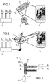
- the figure 1 (extracted from the document [1] cited at the end of the description) illustrates a first possible architecture of such a device provided with two micro-mirrors, respectively called the first micro-mirror 1 1 and second micro-mirror 2 1 , arranged for pivot around, respectively, a first pivot axis X 1 X 1 'and a second pivot axis Y 1 Y 1 ' which are not parallel.
- these two micro-mirrors 1 1 and 2 1 are arranged so that a light beam emitted by a light source 3 1 is reflected by the first micro-mirror 1 1 in the direction of the second micro-mirror 2 1 which it reflects in turn in the direction of, for example, a screen 4 1 .
- the rotation of each of the micro-mirrors 1 1 and 2 1 around their respective pivot axis thus makes it possible to perform a scanning a surface with the light beam, for example for imaging or detection purposes.
- micro-mirrors are also liable to be damaged, in particular by heating induced by the light beam.
- FIG. 2 a second architecture, illustrated on figure 2 (extracted from document [1] cited at the end of the description), can be considered.
- the latter uses a single micro-mirror 1 2 mounted to pivot about two pivot axes X 2 X 2 'and Y 2 Y 2 ' which are not parallel.
- this micro-mirror 1 2 makes it possible to scan the surface of a screen 4 1 by means of a light beam from a light source 3 2 and reflected by said micromirror 1 2 .
- the micro-mirror 1 2 is also likely to undergo heating induced by the light beam.
- this second architecture is also sensitive to the alignment of the light source 3 2 and of the micro-mirror 1 2 .
- the alignment between these two elements is particularly sensitive to the shocks undergone by the device but also to the temperature and pressure conditions imposed on the latter.
- 2D micro-scanners with phase-controlled optical emitter or with optical grating with phase control (“OPA” or “Optical Phased Array” according to Anglo-Saxon terminology) could be proposed.
- the latter may comprise a plurality of optical sources each capable of emitting light radiation.
- Each of its optical sources is also associated with phase modulation means intended to phase shift the optical radiations with respect to each other so as to vary the propagation angle of the combined radiation coming from all of the optical sources.
- the optical sources can come from the same main source.
- This operating principle can be extrapolated to a 2D matrix of optical sources allowing scanning of an optical beam in two different directions, for example perpendicular to one another.
- an object of the present invention is to provide a light scanning device which exhibits flexibility in terms of optical resolution, and / or extent of scanned surface.
- Another object of the present invention is to provide a light scanning device which has appreciable compactness.
- the first and the second beam are arranged so that the bending of one and the other of these two beams allows, respectively, the first and the second beam to sweep, respectively, the first and the second surface in the first direction, along, respectively, a first and a second range of longitudinal angles, the first range of longitudinal angles having a greater extent than that of the second range of longitudinal angles.
- the first and the second movable part are arranged to be subjected to a bending, respectively, of a first and of a second amplitude, the second amplitude being strictly less than the first amplitude.
- the first mobile part has a thickness, called the first thickness, greater than the thickness, called the second thickness, of the second mobile part.
- the first mobile part has a length, called the first length, less than the length, called the second length of the second beam.
- the first mobile part has a frequency of vibration at resonance, called the first frequency, greater than the frequency of vibration at resonance, called the second frequency, of the second mobile part.
- the first and the second scanner respectively comprise a first and a second plurality of waveguides arranged on or in, respectively, the first and the second mobile part, each of the plurality of waveguides. waves being intended to divide the main optical beam into, respectively, a first and second plurality of secondary optical beams.
- the first plurality of waveguides comprises a number of waveguides smaller than that of the second plurality of waveguides.
- the first and the second phase-controlled optical network comprise, respectively, a first and a second plurality of optical phase shifters, each optical phase shifter of the first and of the second plurality of optical phase shifter being coupled to a waveguide, respectively, of the first and of the second plurality of waveguides, advantageously, the second phase-controlled optical network comprises a number of optical phase shifters greater than that of the first phase-controlled optical network.
- each optical phase shifter comprises a diffraction grating coupled to phase shift means intended to impose a phase shift on the secondary optical beam coming from the waveguide to which the optical phase shifter in question is optically coupled.
- the first and the second phase-controlled network are arranged to impose a scanning, respectively, of the first and of the second surface, respectively by the first and the second beam, in the second direction according to , respectively, a first and a second range of side angles, the first range of side angles having a greater extent than the second range of side angles.
- the first and the second beam each comprise, from a front face to a rear face, a front layer, an intermediate layer and a rear layer.
- the front layer and the rear layer each comprise a dielectric material
- the dielectric material advantageously comprises silicon dioxide.
- the first and the second actuator are arranged so that the bending capable of being imposed on one and the other of the first and of the second movable part takes place in a perpendicular plane. to a main face, respectively, of the first and the second beam.
- the first and the second actuator are arranged so that the torsion liable to be imposed on one and the other of the first and of the second mobile part takes place around a axis of elongation, respectively, of the first and the second beam.
- the first and the second actuator each comprise at least one of the means chosen from: electrostatic means, magnetic means, piezoelectric means, thermal means.
- said optical scanner also comprises a support on a main face of which rest, by the first and the second fixed part, the first and the second beam.
- the present invention relates to a scanner provided with a plurality of elementary scanners, and in particular two elementary scanners, called the first and second scanner respectively.
- the first scanner and the second scanner are arranged to scan, each with an optical beam, respectively, a first surface and a second surface included in the first surface and of an extent smaller than the latter.
- FIG 3 schematically illustrates an example of optical scanner 10 according to the present invention.
- the scanner 10 comprises in particular a fixed support 20 provided with a main face 21.
- the support 20 can in particular be obtained from a semiconductor substrate, for example silicon.
- the optical scanner 10 also comprises at least one optical source 50 capable of emitting a main optical beam.
- the main optical beam is advantageously quasi-monochromatic, or even monochromatic.
- the optical source 50 can for example comprise a LASER source.
- the wavelength ⁇ can be between 400 nm and 2500 nm, for example be equal to 905 nm, or equal to 1330 nm or even equal to 1550 nm.
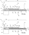
- the optical scanner 10 also comprises at least two elementary scanners 11 called, respectively, first 11 1 and second 11 2 scanners ( figures 4a and 4b ).
- the first 11 1 and the second 11 2 scanners each comprise a so-called first beam 30 1 and second beam 30 2, respectively .
- a beam typically has an elongated shape. More particularly, a beam, according to the present invention, extends, along an axis of elongation, between two ends called, respectively, the fixed end and the free end. More precisely, the first beam 30 1 extends, along a first axis Y 1 Y 1 ', from a first fixed end 33 1 towards a second fixed end 34 1 . In an equivalent manner, the second beam 30 2 extends, along a second axis Y 2 Y 2 ', from a second fixed end 33 2 towards a second free end 34 2 .
- a beam is provided with two faces parallel to each other and, called the front face and the rear face. More precisely, the first beam 30 1 comprises a first front face 31 1 and a first rear face 32 1 . Equivalently, the second beam 30 2 comprises a second front face 31 2 and a second rear face 32 2 .
- a beam may have a thickness between 1 ⁇ m and several hundred ⁇ m, a length between 100 ⁇ m and several millimeters, and a width between 10 ⁇ m and several millimeters.
- the thickness of the beam is defined as the distance between the front face and the back face. Its length is its dimension measured in the direction defined by the axis of elongation while its width is its dimension measured in a direction perpendicular to that defined by the axis of elongation and the thickness of said beam.
- the first axis Y 1 Y 1 'and the second axis Y 2 Y 2 ' are advantageously parallel.
- the first 30 1 and the second beam 30 2 each comprise a movable part 36, called, respectively, the first movable part 36 1 and second movable part 36 2 , as well as a fixed part, called, respectively, the first fixed part 35 1 and second fixed part 35 2 .
- the first 30 1 and the second beam 30 2 are in particular secured to the support 20 by their fixed parts 35 1 and 35 2 .
- the fixed parts 35 1 and 35 2 rest on the main face 21.
- the term “mobile part” is understood to mean a part of a beam capable of undergoing deformation by bending.
- the moving part can be flexed in a direction of a plane comprising the axis of elongation and perpendicular to the front face.
- Each of the two beams 30 1 and 30 2 can comprise, respectively, a first stack and a second stack.
- the first stack may comprise, from the first front face 31 1 towards the first rear face 32 1 , a first front layer 30 a1 , a first intermediate layer 30 b1 , and a first rear layer 30 c1 .
- the second stack may comprise, from the second front face 31 2 to the second rear face 32 2 , a second front layer 30 a2 , a second intermediate layer 30 b2 , and a second rear layer 30 c2 .
- the first front layer 30 a1 , the first rear layer 30 c1 , the second front layer 30 a2 , and the second rear layer 30 c2 may each comprise a dielectric material.
- the dielectric material advantageously comprises silicon dioxide.
- the first intermediate layer 30 b1 and the second intermediate layer 30 b2 advantageously comprise polycrystalline silicon.
- the first 11 1 and the second 11 2 scanners each comprise an actuator, called a first actuator 40 1 and a second actuator 40 2, respectively .
- Each of these actuators 40 1 and 40 2 is in particular designed to impose bending or torsion, respectively, on the first movable part 36 1 and on the second movable part 36 2 .
- the bending of a mobile part capable of being imposed by an actuator corresponds to a deformation or curvature of said mobile part according to a plane, called the bending plane, perpendicular to the front face of the beam, and which includes its axis of elongation.
- a torsion of a movable part corresponds to a deformation of said movable part around its axis of elongation.
- the bending plane of the first beam 30 1 is perpendicular to the first front face 31 1 and includes the first axis Y 1 Y 1 '.
- the bending plane of the second beam 30 2 is perpendicular to the second front face 31 2 and comprises the second axis Y 2 Y 2 ′.
- An actuator according to the present invention can comprise at least one of the means chosen from: electrostatic means, magnetic means, piezoelectric means, thermal means.
- the invention is not however limited to these means alone.
- the actuator can be controlled by control means, for example electronic control means, in particular equipped with a microprocessor or a computer. These control means can in particular be adapted to make the beam vibrate in bending. These control means can in particular impose a vibration on the beam in bending or in torsion. This vibration may in particular have a frequency equal to the resonant frequency of the beam.
- control means for example electronic control means, in particular equipped with a microprocessor or a computer.
- These control means can in particular be adapted to make the beam vibrate in bending.
- These control means can in particular impose a vibration on the beam in bending or in torsion. This vibration may in particular have a frequency equal to the resonant frequency of the beam.
- the actuator can in particular comprise a layer of piezoelectric material interposed between two electrodes intended to impose a non-zero electrical voltage on either side of said layer of piezoelectric material.
- the first actuator 40 1 comprises a first layer of piezoelectric material 40 b1 interposed between a first front electrode A0 a1 and a first rear electrode 40 c1 .
- the second actuator 40 2 comprises a second layer of piezoelectric material 40 b2 interposed between a second front electrode 40 a2 and a second rear electrode 40 c2 .
- first actuator 40 1 and the second actuator 40 2 are each provided, respectively, with first contacts C a1 and C b1 on the one hand, and with two contacts C a2 and C b2 on the other hand, and at the level from which a supply voltage can be applied.
- This supply voltage can in particular be applied with the control means.
- the layer of piezoelectric material contracts, and carries with it the mobile part of the beam in bending.
- the direction of deflection of the piezoelectric material layer may depend on the sign of the electric voltage imposed by the electrodes, in particular when said layer comprises a non-ferroelectric piezoelectric material.
- the deflection amplitude for its part, can depend on many parameters, among which one can cite: the stiffness of the beam, the amplitude of the voltage imposed by the electrodes, the thickness of the layer of piezoelectric material.
- the beam vibrate and more particularly at its resonant frequency in order to give the scanner a better quality factor, and to benefit from the mechanical quality factor to amplify the movement.
- the resonant frequency increases with the thickness and decreases as its length increases. This reduction as a function of the thickness nevertheless follows a squared law and is therefore more marked when it comes to modifying the length.
- the resonant frequency of the beam can be adjusted by its thickness and length.
- the layer of piezoelectric material can comprise at least one of the materials chosen from: PZT (lead titano-zirconate) or AIN (aluminum nitride). Other piezoelectric materials can be envisaged.
- the first 11 1 and the second 11 2 scanners can also each comprise a plurality of waveguides, called, respectively, the first 60 i1 and second 60 i2 plurality of waveguides arranged on or in, respectively, the first 36 1 and the second 36 2 mobile part ( figure 6 ).
- the waveguides illustrated on figure 6 are arranged parallel to the axis of elongation, and so that the ratio between their spacing (in ⁇ m) and the wavelength ⁇ (in nm) is between 0.5 and 10.
- the waveguides can for example be of a length of between a hundred microns and ten millimeters, and be spaced from each other by a distance of between a hundred microns and ten millimeters.
- Each of the plurality of waveguides 60 i and 60 i2 is intended in particular to divide the main optical beam into, respectively, a first and second plurality of secondary optical beams.
- the coupling of the optical source 50 with the waveguides can be carried out with coupling means 51 ( figures 3 , 4a and 4b ) and in particular with one or more optical fibers.
- An elementary scanner according to the present invention also comprises a phase-controlled optical network arranged in or on the mobile part of the elementary scanner from which the main optical beam emitted for the optical source 50 is partly extracted in the form of an extracted beam. .
- the phase-controlled network can be controlled by the control means.
- the phase-controlled optical network of the first scanner 11 1 is arranged to allow the extraction of the main optical beam in the form of a first beam
- the phase-controlled optical network of the second scanner 11 2 is arranged to allow the extraction of the main optical beam in the form of a second beam.
- the first phase-controlled optical network 70 1 and the second phase-controlled optical network 70 2 each comprise a plurality of phase shifters, called, respectively, the first plurality of phase shifters 70 i1 and second plurality of phase shifters 70 i2 .
- Each phase shifter of the first and of the second plurality of optical phase shifters is advantageously coupled to a waveguide, respectively, of the first and of the second plurality of waveguides.
- each optical phase shifter 70 i1 and 70 i2 comprises a diffraction grating coupled to phase shifting means intended to impose a phase shift on the secondary optical beam coming from the waveguide to which the optical phase shifter in question is optically coupled.
- the figure 7 is an illustration of an optical phase shifter according to a first architecture capable of being implemented in the context of the present invention.
- the diffraction grating is formed of pads aligned in the extension of the waveguide, while the phase shifting means may include a heating element placed directly above the waveguide and intended to locally heat the latter in order to to modulate its refractive index.
- the figure 8 is an illustration of an optical phase shifter according to a second architecture capable of being implemented within the framework of the present invention.
- the diffraction grating is formed of aligned solid arcs, while the phase shifting means may comprise a heating element intended to locally heat the waveguide 60i in order to modulate its refractive index.
- the waveguides and / or the diffraction gratings can comprise silicon nitride.
- the optical phase shifters can be arranged in a line perpendicular to the axis of elongation of the beam.
- the optical phase shifters can be arranged in a matrix fashion.
- an elementary scanner can thus scan space according to two propagation angles.
- An elementary scanner, as described above, in operation, is thus able to scan a surface S by means of the extracted beam.
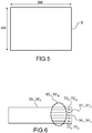
- the surface S is represented as a rectangle at the figure 5 .
- the latter can correspond to the surface of an object, and more particularly the surface of a 3-dimensional object.
- the scanning of said surface can be executed in a first direction AA 'and in a second direction BB' ( figure 5 ), which can advantageously be perpendicular to each other.
- the scanning of the surface S in the first direction AA ′ is notably ensured by the bending of the beam forming the elementary scanner.
- the extracted beam is emitted in a direction, called the direction at rest (called the first direction at rest Z 1 Z 1 'for the first scanner and second direction at rest Z 2 Z 2 'for the second scanner).
- the position at rest can in particular be perpendicular to the front face of the beam at rest.
- this longitudinal angle can vary in a range of longitudinal angles ⁇ imposed by the physical and geometric parameters of the beam.
- the scanning of the surface S in the second direction BB ′ is provided by the phase-controlled optical network of the elementary scanner.
- the phase-controlled optical network imposes a deflection on the extracted beam, at an angle ⁇ , called lateral angle, with respect to the direction at rest and in a plane, called lateral plane, perpendicular to the plane of flexion and which includes the direction at rest.
- this lateral angle can vary within a range of lateral angles ⁇ imposed by the physical and geometric parameters of the phase-controlled optical network.
- the first scanner 11 1 is arranged to scan a first surface S1 along one and the other of the first range of longitudinal angles ⁇ 1 and of the second range of lateral angles ⁇ 1
- the second scanner 11 2 is arranged to scan a second surface S2 along one and the other of the second range of longitudinal angles ⁇ 2 and of the second range of lateral angles ⁇ 2 .
- This variation in the scanning of longitudinal angles can be modulated by the polarization applied to the piezoelectric material.
- the second surface S2 is of an extent smaller than that of the first surface S1 and is included in the first surface S1 ( figure 9 ).
- the second scanner 11 2 is arranged to scan a section of the surface scanned by the first scanner 11 1 . This arrangement thus makes it possible to scan a surface, for example for imaging purposes with different levels of resolution, without however affecting the compactness of the optical scanner 10.
- the first scanner 11 1 and the second scanner 11 2 are arranged so that the second range of longitudinal angles ⁇ 2 is smaller than the first range of longitudinal angles ⁇ 1 .
- this limitation can in particular be imposed by a different polarization of the beams.
- the higher the electric polarization field imposed on the layer of piezoelectric material for example a layer of PZT
- the greater the bending of all formed by said layer and beam is important. This bending is dependent not only on the mechanical and geometric properties of the beam but also on the electric polarization field imposed on the layer of piezoelectric material.
- this limitation can in particular be imposed by beams of different lengths in the context of operation at the resonant frequency.
- the amplitude of deflection of a beam, for a given load is directly proportional to the power of four of its length and inversely proportional to the product of its thickness by its moment of inertia.
- the amplitude of deflection of a beam increases with its length and / or when its thickness decreases.
- the first beam advantageously has a length, called the first length L1, less than the length, called the second length L2, of the second beam.
- the first beam advantageously has a thickness, called thickness E1, greater than the thickness, called second thickness E2, of the second beam.
- the resonance frequency of a beam is proportional to its thickness and inversely proportional to the square of its length.
- the first beam also has a resonant frequency higher than that of the second beam.
- the first beam has a resonant frequency greater than that of the second beam.
- the optical scanner according to the present invention makes it possible to scan the first surface, with the first scanner, at a relatively high frequency, for example to rapidly detect an area of interest and intended to be scanned this time with the second scanner.
- the scan with the second scanner is then performed at a higher resolution to reveal details within the area of interest that went unnoticed on the first scan.
- This resolution can in particular be adjusted by the number and / or the density of waveguides, and / or the device for extracting the light from each waveguide.
- the first and the second phase-controlled network are arranged so that the first range of lateral angles has a greater extent than that of the second range of lateral angles.
- the second phase-controlled network has a resolution greater than that of the first phase-controlled network. This result can in particular be achieved by forming a second phase-controlled network which comprises a greater number (or a greater density) of optical phase shifters than the first phase-controlled network.
- the optical scanner is not limited to two elementary scanners and may include a greater number of them.
- the figure 10 schematically represents an optical scanner provided with four elementary scanners, forming two pairs of elementary scanners. Each of the two pairs includes a first scanner and a second scanner as described above.
- the optical scanner according to the present invention thus makes it possible to respond to the problems relating to the resolution of the scanning while maintaining the compactness of said scanner.
- this optical scanner which does not use micro-mirrors, does not require alignment and remains simple to use.
- the beams of the different elementary scanners can advantageously be formed collectively.
- the figures 11 to 16 represent steps in the manufacture of a first beam and of a second beam of different thicknesses and capable of being implemented within the framework of a method of manufacturing an optical scanner.
- the method comprises a step a) of forming a silicon oxide layer 110 by thermal oxidation of a silicon substrate 100.
- step a) is then followed by a step b) which comprises a photolithography / etching sequence intended to delimit the second beam 30 2 .
- step b) comprises a photolithography / etching sequence intended to delimit the second beam 30 2 .
- the remainder of the layer 110 at the end of step b) forms the second rear layer 30 c2 of the second beam.
- the assembly is then covered with a layer of poly silicon 120 which is optionally flattened.
- a step c) of forming the first rear layer 30 c1 is then carried out.
- This step may in particular involve, in order, the deposition of a layer of silicon oxide, and a photolithography / etching sequence in order to delimit in said layer of silicon oxide the first rear layer 30 c1 .
- a step d) of forming another layer of polycrystalline silicon is carried out. This other layer covers the layer of polycrystalline silicon and the first rear layer 30 c1 .
- the first front layer 30 a1 and the second front layer 30 a2 are then formed during the execution of a step e).
- This step can involve the formation of a silicon oxide layer followed by a photolithography / etching sequence.
- An etching step f) can then be carried out in order to free the first beam 30 1 and the second beam 30 2 which each have a different thickness.
- the scanner 10 according to the present invention can advantageously be implemented in an image projector of reduced size (for example a pico-projector) in mobile electronic equipment, and more particularly, an image projector.
- an image projector for example a pico-projector
- mobile phone a connected watch
- intra-retinal projection equipment for augmented reality
- the scanner can also be used in the context of 3D applications, and in particular 3D imaging.
- the scanner 10 can also form the active part of a LIDAR, and for example be implemented in an autonomous vehicle.
Landscapes
- Physics & Mathematics (AREA)
- General Physics & Mathematics (AREA)
- Optics & Photonics (AREA)
- Mechanical Optical Scanning Systems (AREA)
- Mechanical Light Control Or Optical Switches (AREA)
Applications Claiming Priority (1)
| Application Number | Priority Date | Filing Date | Title |
|---|---|---|---|
| FR2006927A FR3112217B1 (fr) | 2020-07-01 | 2020-07-01 | Scanner optique |
Publications (2)
| Publication Number | Publication Date |
|---|---|
| EP3933484A1 true EP3933484A1 (de) | 2022-01-05 |
| EP3933484B1 EP3933484B1 (de) | 2022-12-28 |
Family
ID=73038109
Family Applications (1)
| Application Number | Title | Priority Date | Filing Date |
|---|---|---|---|
| EP21180310.1A Active EP3933484B1 (de) | 2020-07-01 | 2021-06-18 | Optischer scanner |
Country Status (3)
| Country | Link |
|---|---|
| US (1) | US12189116B2 (de) |
| EP (1) | EP3933484B1 (de) |
| FR (1) | FR3112217B1 (de) |
Families Citing this family (1)
| Publication number | Priority date | Publication date | Assignee | Title |
|---|---|---|---|---|
| FR3166218A1 (fr) | 2024-09-06 | 2026-03-13 | Commissariat à l'Energie Atomique et aux Energies Alternatives | Structure micromécanique pour capteur optique |
Citations (2)
| Publication number | Priority date | Publication date | Assignee | Title |
|---|---|---|---|---|
| FR2923092A1 (fr) * | 2007-10-31 | 2009-05-01 | Thales Sa | Source laser comportant un dispositif de balayage angulaire. |
| WO2018222727A1 (en) * | 2017-05-31 | 2018-12-06 | Cornell University | Multidimensional piezoelectric actuator having enhanced actuation range |
Family Cites Families (3)
| Publication number | Priority date | Publication date | Assignee | Title |
|---|---|---|---|---|
| JP5458837B2 (ja) * | 2009-03-16 | 2014-04-02 | 株式会社リコー | 光走査装置 |
| US12360361B2 (en) * | 2017-12-26 | 2025-07-15 | Adhawk Microsystems Inc. | Advanced packaging for compact object-scanning modules |
| WO2023018945A1 (en) * | 2021-08-12 | 2023-02-16 | Ouster, Inc. | Coaxial lidar system using a diffractive waveguide |
-
2020
- 2020-07-01 FR FR2006927A patent/FR3112217B1/fr active Active
-
2021
- 2021-06-18 EP EP21180310.1A patent/EP3933484B1/de active Active
- 2021-06-28 US US17/304,871 patent/US12189116B2/en active Active
Patent Citations (2)
| Publication number | Priority date | Publication date | Assignee | Title |
|---|---|---|---|---|
| FR2923092A1 (fr) * | 2007-10-31 | 2009-05-01 | Thales Sa | Source laser comportant un dispositif de balayage angulaire. |
| WO2018222727A1 (en) * | 2017-05-31 | 2018-12-06 | Cornell University | Multidimensional piezoelectric actuator having enhanced actuation range |
Non-Patent Citations (3)
| Title |
|---|
| HOLMSTROM SVEN T S ET AL: "MEMS Laser Scanners: A Review", JOURNAL OF MICROELECTROMECHANICAL SYSTEMS, IEEE SERVICE CENTER, US, vol. 23, no. 2, 1 April 2014 (2014-04-01), pages 259 - 275, XP011544460, ISSN: 1057-7157, [retrieved on 20140331], DOI: 10.1109/JMEMS.2013.2295470 * |
| JIE SUN ET AL.: "Large-scale nanophotonic phased array", NATURE, vol. 493, January 2013 (2013-01-01), pages 195 - 199, XP055124083, DOI: 10.1038/nature11727 |
| SVEN HOLMSTROM ET AL.: "MEMS laser scanners : a review", JOURNAL OF MICROELECTROMECHANICAL SYSTEMS, April 2014 (2014-04-01) |
Also Published As
| Publication number | Publication date |
|---|---|
| FR3112217A1 (fr) | 2022-01-07 |
| US20220003987A1 (en) | 2022-01-06 |
| US12189116B2 (en) | 2025-01-07 |
| FR3112217B1 (fr) | 2022-07-08 |
| EP3933484B1 (de) | 2022-12-28 |
Similar Documents
| Publication | Publication Date | Title |
|---|---|---|
| EP0722103B1 (de) | Optische Vorrichtung für optomechanische Anwendung | |
| EP2171503B1 (de) | Optische vorrichtung mit mittel zur betätigung einer kompakten verformbaren membran | |
| EP2866000B1 (de) | Optomechanische Vorrichtung zum Betätigen und/oder Erkennen einer Bewegung eines mechanischen Elements, insbesondere für die gravimetrische Erfassung | |
| CN102466516A (zh) | 光学装置 | |
| Wang et al. | Micromirror based optical phased array for wide-angle beamsteering | |
| EP3933484B1 (de) | Optischer scanner | |
| EP0742459B1 (de) | Optomechanischer Mikro-Strahlablenker unter Verwendung der Verschiebung von Mikrolinsen | |
| EP3933483B1 (de) | Optischer scanner | |
| EP3933485B1 (de) | Optischer scanner | |
| EP3926392A1 (de) | Optische vorrichtung und ihr herstellungsverfahren | |
| EP3764148B1 (de) | Scanner mit optischer netzeinheit mit mobiler phasensteuerung | |
| EP3514614A1 (de) | Optische vorrichtung | |
| EP3647738A1 (de) | Optomechanischer resonator mit wellenleiter mit subwellenlänge | |
| FR3141257A1 (fr) | Elément optique holographique et son procédé de fabrication | |
| EP4075182A1 (de) | Optischer scanner | |
| EP2354832A1 (de) | Bimorphes optisches Element | |
| EP4078219B1 (de) | Optoelektronisches bauelement, das auf einem einzigen substrat einen optischen wandler aus einem halbleitermaterial iii-v und ein optisch abtastendes mikroelektromechanisches system umfasst | |
| Bartek et al. | Micromachined Fabry-Perot optical filters | |
| EP4707913A1 (de) | Mikromechanische struktur für einen optischen sensor | |
| EP4553561A1 (de) | Reflektorvorrichtung mit einem detektor und verfahren dafür | |
| KR20060031450A (ko) | 경사진 광투과성 덮개를 가진 광변조기 패키지 | |
| EP4707908A1 (de) | Bildanzeigevorrichtung | |
| WO2025061700A1 (fr) | Systeme de guide optique amélioré et dispositif d'affichage pres de l'œil comportant un tel systeme | |
| EP1706769A1 (de) | Optisches ablenk-array |
Legal Events
| Date | Code | Title | Description |
|---|---|---|---|
| PUAI | Public reference made under article 153(3) epc to a published international application that has entered the european phase |
Free format text: ORIGINAL CODE: 0009012 |
|
| STAA | Information on the status of an ep patent application or granted ep patent |
Free format text: STATUS: REQUEST FOR EXAMINATION WAS MADE |
|
| 17P | Request for examination filed |
Effective date: 20210618 |
|
| AK | Designated contracting states |
Kind code of ref document: A1 Designated state(s): AL AT BE BG CH CY CZ DE DK EE ES FI FR GB GR HR HU IE IS IT LI LT LU LV MC MK MT NL NO PL PT RO RS SE SI SK SM TR |
|
| B565 | Issuance of search results under rule 164(2) epc |
Effective date: 20211104 |
|
| GRAP | Despatch of communication of intention to grant a patent |
Free format text: ORIGINAL CODE: EPIDOSNIGR1 |
|
| STAA | Information on the status of an ep patent application or granted ep patent |
Free format text: STATUS: GRANT OF PATENT IS INTENDED |
|
| RIC1 | Information provided on ipc code assigned before grant |
Ipc: G02B 27/00 20060101ALI20220620BHEP Ipc: G02B 26/10 20060101ALI20220620BHEP Ipc: G02B 26/06 20060101AFI20220620BHEP |
|
| INTG | Intention to grant announced |
Effective date: 20220720 |
|
| GRAS | Grant fee paid |
Free format text: ORIGINAL CODE: EPIDOSNIGR3 |
|
| GRAA | (expected) grant |
Free format text: ORIGINAL CODE: 0009210 |
|
| STAA | Information on the status of an ep patent application or granted ep patent |
Free format text: STATUS: THE PATENT HAS BEEN GRANTED |
|
| AK | Designated contracting states |
Kind code of ref document: B1 Designated state(s): AL AT BE BG CH CY CZ DE DK EE ES FI FR GB GR HR HU IE IS IT LI LT LU LV MC MK MT NL NO PL PT RO RS SE SI SK SM TR |
|
| REG | Reference to a national code |
Ref country code: GB Ref legal event code: FG4D Free format text: NOT ENGLISH |
|
| REG | Reference to a national code |
Ref country code: CH Ref legal event code: EP |
|
| REG | Reference to a national code |
Ref country code: DE Ref legal event code: R096 Ref document number: 602021001100 Country of ref document: DE |
|
| REG | Reference to a national code |
Ref country code: AT Ref legal event code: REF Ref document number: 1540852 Country of ref document: AT Kind code of ref document: T Effective date: 20230115 |
|
| REG | Reference to a national code |
Ref country code: IE Ref legal event code: FG4D Free format text: LANGUAGE OF EP DOCUMENT: FRENCH |
|
| REG | Reference to a national code |
Ref country code: LT Ref legal event code: MG9D |
|
| PG25 | Lapsed in a contracting state [announced via postgrant information from national office to epo] |
Ref country code: SE Free format text: LAPSE BECAUSE OF FAILURE TO SUBMIT A TRANSLATION OF THE DESCRIPTION OR TO PAY THE FEE WITHIN THE PRESCRIBED TIME-LIMIT Effective date: 20221228 Ref country code: NO Free format text: LAPSE BECAUSE OF FAILURE TO SUBMIT A TRANSLATION OF THE DESCRIPTION OR TO PAY THE FEE WITHIN THE PRESCRIBED TIME-LIMIT Effective date: 20230328 Ref country code: LT Free format text: LAPSE BECAUSE OF FAILURE TO SUBMIT A TRANSLATION OF THE DESCRIPTION OR TO PAY THE FEE WITHIN THE PRESCRIBED TIME-LIMIT Effective date: 20221228 Ref country code: FI Free format text: LAPSE BECAUSE OF FAILURE TO SUBMIT A TRANSLATION OF THE DESCRIPTION OR TO PAY THE FEE WITHIN THE PRESCRIBED TIME-LIMIT Effective date: 20221228 |
|
| REG | Reference to a national code |
Ref country code: NL Ref legal event code: MP Effective date: 20221228 |
|
| REG | Reference to a national code |
Ref country code: AT Ref legal event code: MK05 Ref document number: 1540852 Country of ref document: AT Kind code of ref document: T Effective date: 20221228 |
|
| PG25 | Lapsed in a contracting state [announced via postgrant information from national office to epo] |
Ref country code: RS Free format text: LAPSE BECAUSE OF FAILURE TO SUBMIT A TRANSLATION OF THE DESCRIPTION OR TO PAY THE FEE WITHIN THE PRESCRIBED TIME-LIMIT Effective date: 20221228 Ref country code: LV Free format text: LAPSE BECAUSE OF FAILURE TO SUBMIT A TRANSLATION OF THE DESCRIPTION OR TO PAY THE FEE WITHIN THE PRESCRIBED TIME-LIMIT Effective date: 20221228 Ref country code: HR Free format text: LAPSE BECAUSE OF FAILURE TO SUBMIT A TRANSLATION OF THE DESCRIPTION OR TO PAY THE FEE WITHIN THE PRESCRIBED TIME-LIMIT Effective date: 20221228 Ref country code: GR Free format text: LAPSE BECAUSE OF FAILURE TO SUBMIT A TRANSLATION OF THE DESCRIPTION OR TO PAY THE FEE WITHIN THE PRESCRIBED TIME-LIMIT Effective date: 20230329 |
|
| PG25 | Lapsed in a contracting state [announced via postgrant information from national office to epo] |
Ref country code: NL Free format text: LAPSE BECAUSE OF FAILURE TO SUBMIT A TRANSLATION OF THE DESCRIPTION OR TO PAY THE FEE WITHIN THE PRESCRIBED TIME-LIMIT Effective date: 20221228 |
|
| PG25 | Lapsed in a contracting state [announced via postgrant information from national office to epo] |
Ref country code: SM Free format text: LAPSE BECAUSE OF FAILURE TO SUBMIT A TRANSLATION OF THE DESCRIPTION OR TO PAY THE FEE WITHIN THE PRESCRIBED TIME-LIMIT Effective date: 20221228 Ref country code: RO Free format text: LAPSE BECAUSE OF FAILURE TO SUBMIT A TRANSLATION OF THE DESCRIPTION OR TO PAY THE FEE WITHIN THE PRESCRIBED TIME-LIMIT Effective date: 20221228 Ref country code: PT Free format text: LAPSE BECAUSE OF FAILURE TO SUBMIT A TRANSLATION OF THE DESCRIPTION OR TO PAY THE FEE WITHIN THE PRESCRIBED TIME-LIMIT Effective date: 20230428 Ref country code: ES Free format text: LAPSE BECAUSE OF FAILURE TO SUBMIT A TRANSLATION OF THE DESCRIPTION OR TO PAY THE FEE WITHIN THE PRESCRIBED TIME-LIMIT Effective date: 20221228 Ref country code: EE Free format text: LAPSE BECAUSE OF FAILURE TO SUBMIT A TRANSLATION OF THE DESCRIPTION OR TO PAY THE FEE WITHIN THE PRESCRIBED TIME-LIMIT Effective date: 20221228 Ref country code: CZ Free format text: LAPSE BECAUSE OF FAILURE TO SUBMIT A TRANSLATION OF THE DESCRIPTION OR TO PAY THE FEE WITHIN THE PRESCRIBED TIME-LIMIT Effective date: 20221228 Ref country code: AT Free format text: LAPSE BECAUSE OF FAILURE TO SUBMIT A TRANSLATION OF THE DESCRIPTION OR TO PAY THE FEE WITHIN THE PRESCRIBED TIME-LIMIT Effective date: 20221228 |
|
| PG25 | Lapsed in a contracting state [announced via postgrant information from national office to epo] |
Ref country code: SK Free format text: LAPSE BECAUSE OF FAILURE TO SUBMIT A TRANSLATION OF THE DESCRIPTION OR TO PAY THE FEE WITHIN THE PRESCRIBED TIME-LIMIT Effective date: 20221228 Ref country code: PL Free format text: LAPSE BECAUSE OF FAILURE TO SUBMIT A TRANSLATION OF THE DESCRIPTION OR TO PAY THE FEE WITHIN THE PRESCRIBED TIME-LIMIT Effective date: 20221228 Ref country code: IS Free format text: LAPSE BECAUSE OF FAILURE TO SUBMIT A TRANSLATION OF THE DESCRIPTION OR TO PAY THE FEE WITHIN THE PRESCRIBED TIME-LIMIT Effective date: 20230428 Ref country code: AL Free format text: LAPSE BECAUSE OF FAILURE TO SUBMIT A TRANSLATION OF THE DESCRIPTION OR TO PAY THE FEE WITHIN THE PRESCRIBED TIME-LIMIT Effective date: 20221228 |
|
| REG | Reference to a national code |
Ref country code: DE Ref legal event code: R097 Ref document number: 602021001100 Country of ref document: DE |
|
| PG25 | Lapsed in a contracting state [announced via postgrant information from national office to epo] |
Ref country code: DK Free format text: LAPSE BECAUSE OF FAILURE TO SUBMIT A TRANSLATION OF THE DESCRIPTION OR TO PAY THE FEE WITHIN THE PRESCRIBED TIME-LIMIT Effective date: 20221228 |
|
| PLBE | No opposition filed within time limit |
Free format text: ORIGINAL CODE: 0009261 |
|
| STAA | Information on the status of an ep patent application or granted ep patent |
Free format text: STATUS: NO OPPOSITION FILED WITHIN TIME LIMIT |
|
| 26N | No opposition filed |
Effective date: 20230929 |
|
| PG25 | Lapsed in a contracting state [announced via postgrant information from national office to epo] |
Ref country code: MC Free format text: LAPSE BECAUSE OF FAILURE TO SUBMIT A TRANSLATION OF THE DESCRIPTION OR TO PAY THE FEE WITHIN THE PRESCRIBED TIME-LIMIT Effective date: 20221228 |
|
| PG25 | Lapsed in a contracting state [announced via postgrant information from national office to epo] |
Ref country code: SI Free format text: LAPSE BECAUSE OF FAILURE TO SUBMIT A TRANSLATION OF THE DESCRIPTION OR TO PAY THE FEE WITHIN THE PRESCRIBED TIME-LIMIT Effective date: 20221228 Ref country code: MC Free format text: LAPSE BECAUSE OF FAILURE TO SUBMIT A TRANSLATION OF THE DESCRIPTION OR TO PAY THE FEE WITHIN THE PRESCRIBED TIME-LIMIT Effective date: 20221228 |
|
| REG | Reference to a national code |
Ref country code: BE Ref legal event code: MM Effective date: 20230630 |
|
| PG25 | Lapsed in a contracting state [announced via postgrant information from national office to epo] |
Ref country code: LU Free format text: LAPSE BECAUSE OF NON-PAYMENT OF DUE FEES Effective date: 20230618 |
|
| REG | Reference to a national code |
Ref country code: IE Ref legal event code: MM4A |
|
| PG25 | Lapsed in a contracting state [announced via postgrant information from national office to epo] |
Ref country code: LU Free format text: LAPSE BECAUSE OF NON-PAYMENT OF DUE FEES Effective date: 20230618 |
|
| PG25 | Lapsed in a contracting state [announced via postgrant information from national office to epo] |
Ref country code: IE Free format text: LAPSE BECAUSE OF NON-PAYMENT OF DUE FEES Effective date: 20230618 |
|
| PG25 | Lapsed in a contracting state [announced via postgrant information from national office to epo] |
Ref country code: IE Free format text: LAPSE BECAUSE OF NON-PAYMENT OF DUE FEES Effective date: 20230618 |
|
| PG25 | Lapsed in a contracting state [announced via postgrant information from national office to epo] |
Ref country code: BE Free format text: LAPSE BECAUSE OF NON-PAYMENT OF DUE FEES Effective date: 20230630 |
|
| PG25 | Lapsed in a contracting state [announced via postgrant information from national office to epo] |
Ref country code: BG Free format text: LAPSE BECAUSE OF FAILURE TO SUBMIT A TRANSLATION OF THE DESCRIPTION OR TO PAY THE FEE WITHIN THE PRESCRIBED TIME-LIMIT Effective date: 20221228 |
|
| PG25 | Lapsed in a contracting state [announced via postgrant information from national office to epo] |
Ref country code: BG Free format text: LAPSE BECAUSE OF FAILURE TO SUBMIT A TRANSLATION OF THE DESCRIPTION OR TO PAY THE FEE WITHIN THE PRESCRIBED TIME-LIMIT Effective date: 20221228 |
|
| REG | Reference to a national code |
Ref country code: CH Ref legal event code: PL |
|
| PG25 | Lapsed in a contracting state [announced via postgrant information from national office to epo] |
Ref country code: CH Free format text: LAPSE BECAUSE OF NON-PAYMENT OF DUE FEES Effective date: 20240630 |
|
| PGFP | Annual fee paid to national office [announced via postgrant information from national office to epo] |
Ref country code: DE Payment date: 20250618 Year of fee payment: 5 |
|
| PGFP | Annual fee paid to national office [announced via postgrant information from national office to epo] |
Ref country code: GB Payment date: 20250625 Year of fee payment: 5 |
|
| PGFP | Annual fee paid to national office [announced via postgrant information from national office to epo] |
Ref country code: FR Payment date: 20250623 Year of fee payment: 5 |
|
| PG25 | Lapsed in a contracting state [announced via postgrant information from national office to epo] |
Ref country code: CY Free format text: LAPSE BECAUSE OF FAILURE TO SUBMIT A TRANSLATION OF THE DESCRIPTION OR TO PAY THE FEE WITHIN THE PRESCRIBED TIME-LIMIT; INVALID AB INITIO Effective date: 20210618 |
|
| PG25 | Lapsed in a contracting state [announced via postgrant information from national office to epo] |
Ref country code: HU Free format text: LAPSE BECAUSE OF FAILURE TO SUBMIT A TRANSLATION OF THE DESCRIPTION OR TO PAY THE FEE WITHIN THE PRESCRIBED TIME-LIMIT; INVALID AB INITIO Effective date: 20210618 |
|
| PGFP | Annual fee paid to national office [announced via postgrant information from national office to epo] |
Ref country code: IT Payment date: 20250630 Year of fee payment: 5 |
|
| PG25 | Lapsed in a contracting state [announced via postgrant information from national office to epo] |
Ref country code: TR Free format text: LAPSE BECAUSE OF FAILURE TO SUBMIT A TRANSLATION OF THE DESCRIPTION OR TO PAY THE FEE WITHIN THE PRESCRIBED TIME-LIMIT Effective date: 20221228 |