EP4078219B1 - Optoelektronisches bauelement, das auf einem einzigen substrat einen optischen wandler aus einem halbleitermaterial iii-v und ein optisch abtastendes mikroelektromechanisches system umfasst - Google Patents
Optoelektronisches bauelement, das auf einem einzigen substrat einen optischen wandler aus einem halbleitermaterial iii-v und ein optisch abtastendes mikroelektromechanisches system umfasst Download PDFInfo
- Publication number
- EP4078219B1 EP4078219B1 EP20835812.7A EP20835812A EP4078219B1 EP 4078219 B1 EP4078219 B1 EP 4078219B1 EP 20835812 A EP20835812 A EP 20835812A EP 4078219 B1 EP4078219 B1 EP 4078219B1
- Authority
- EP
- European Patent Office
- Prior art keywords
- layer
- silicon
- optoelectronic component
- iii
- mirror
- Prior art date
- Legal status (The legal status is an assumption and is not a legal conclusion. Google has not performed a legal analysis and makes no representation as to the accuracy of the status listed.)
- Active
Links
Images



Classifications
-
- H—ELECTRICITY
- H10—SEMICONDUCTOR DEVICES; ELECTRIC SOLID-STATE DEVICES NOT OTHERWISE PROVIDED FOR
- H10N—ELECTRIC SOLID-STATE DEVICES NOT OTHERWISE PROVIDED FOR
- H10N30/00—Piezoelectric or electrostrictive devices
- H10N30/50—Piezoelectric or electrostrictive devices having a stacked or multilayer structure
-
- B—PERFORMING OPERATIONS; TRANSPORTING
- B81—MICROSTRUCTURAL TECHNOLOGY
- B81B—MICROSTRUCTURAL DEVICES OR SYSTEMS, e.g. MICROMECHANICAL DEVICES
- B81B3/00—Devices comprising flexible or deformable elements, e.g. comprising elastic tongues or membranes
- B81B3/0018—Structures acting upon the moving or flexible element for transforming energy into mechanical movement or vice versa, i.e. actuators, sensors, generators
- B81B3/0027—Structures for transforming mechanical energy, e.g. potential energy of a spring into translation, sound into translation
-
- G—PHYSICS
- G01—MEASURING; TESTING
- G01S—RADIO DIRECTION-FINDING; RADIO NAVIGATION; DETERMINING DISTANCE OR VELOCITY BY USE OF RADIO WAVES; LOCATING OR PRESENCE-DETECTING BY USE OF THE REFLECTION OR RERADIATION OF RADIO WAVES; ANALOGOUS ARRANGEMENTS USING OTHER WAVES
- G01S17/00—Systems using the reflection or reradiation of electromagnetic waves other than radio waves, e.g. lidar systems
- G01S17/02—Systems using the reflection of electromagnetic waves other than radio waves
- G01S17/06—Systems determining position data of a target
- G01S17/42—Simultaneous measurement of distance and other co-ordinates
-
- G—PHYSICS
- G01—MEASURING; TESTING
- G01S—RADIO DIRECTION-FINDING; RADIO NAVIGATION; DETERMINING DISTANCE OR VELOCITY BY USE OF RADIO WAVES; LOCATING OR PRESENCE-DETECTING BY USE OF THE REFLECTION OR RERADIATION OF RADIO WAVES; ANALOGOUS ARRANGEMENTS USING OTHER WAVES
- G01S7/00—Details of systems according to groups G01S13/00, G01S15/00, G01S17/00
- G01S7/48—Details of systems according to groups G01S13/00, G01S15/00, G01S17/00 of systems according to group G01S17/00
- G01S7/481—Constructional features, e.g. arrangements of optical elements
- G01S7/4811—Constructional features, e.g. arrangements of optical elements common to transmitter and receiver
- G01S7/4813—Housing arrangements
-
- G—PHYSICS
- G01—MEASURING; TESTING
- G01S—RADIO DIRECTION-FINDING; RADIO NAVIGATION; DETERMINING DISTANCE OR VELOCITY BY USE OF RADIO WAVES; LOCATING OR PRESENCE-DETECTING BY USE OF THE REFLECTION OR RERADIATION OF RADIO WAVES; ANALOGOUS ARRANGEMENTS USING OTHER WAVES
- G01S7/00—Details of systems according to groups G01S13/00, G01S15/00, G01S17/00
- G01S7/48—Details of systems according to groups G01S13/00, G01S15/00, G01S17/00 of systems according to group G01S17/00
- G01S7/481—Constructional features, e.g. arrangements of optical elements
- G01S7/4817—Constructional features, e.g. arrangements of optical elements relating to scanning
-
- G—PHYSICS
- G02—OPTICS
- G02B—OPTICAL ELEMENTS, SYSTEMS OR APPARATUS
- G02B26/00—Optical devices or arrangements for the control of light using movable or deformable optical elements
- G02B26/08—Optical devices or arrangements for the control of light using movable or deformable optical elements for controlling the direction of light
- G02B26/0816—Optical devices or arrangements for the control of light using movable or deformable optical elements for controlling the direction of light by means of one or more reflecting elements
- G02B26/0833—Optical devices or arrangements for the control of light using movable or deformable optical elements for controlling the direction of light by means of one or more reflecting elements the reflecting element being a micromechanical device, e.g. a MEMS mirror, DMD
-
- G—PHYSICS
- G02—OPTICS
- G02B—OPTICAL ELEMENTS, SYSTEMS OR APPARATUS
- G02B26/00—Optical devices or arrangements for the control of light using movable or deformable optical elements
- G02B26/08—Optical devices or arrangements for the control of light using movable or deformable optical elements for controlling the direction of light
- G02B26/10—Scanning systems
- G02B26/105—Scanning systems with one or more pivoting mirrors or galvano-mirrors
-
- H—ELECTRICITY
- H10—SEMICONDUCTOR DEVICES; ELECTRIC SOLID-STATE DEVICES NOT OTHERWISE PROVIDED FOR
- H10N—ELECTRIC SOLID-STATE DEVICES NOT OTHERWISE PROVIDED FOR
- H10N30/00—Piezoelectric or electrostrictive devices
- H10N30/80—Constructional details
- H10N30/85—Piezoelectric or electrostrictive active materials
- H10N30/852—Composite materials, e.g. having 1-3 or 2-2 type connectivity
-
- B—PERFORMING OPERATIONS; TRANSPORTING
- B81—MICROSTRUCTURAL TECHNOLOGY
- B81B—MICROSTRUCTURAL DEVICES OR SYSTEMS, e.g. MICROMECHANICAL DEVICES
- B81B2203/00—Basic microelectromechanical structures
- B81B2203/05—Type of movement
- B81B2203/051—Translation according to an axis parallel to the substrate
-
- H—ELECTRICITY
- H01—ELECTRIC ELEMENTS
- H01S—DEVICES USING THE PROCESS OF LIGHT AMPLIFICATION BY STIMULATED EMISSION OF RADIATION [LASER] TO AMPLIFY OR GENERATE LIGHT; DEVICES USING STIMULATED EMISSION OF ELECTROMAGNETIC RADIATION IN WAVE RANGES OTHER THAN OPTICAL
- H01S5/00—Semiconductor lasers
- H01S5/005—Optical components external to the laser cavity, specially adapted therefor, e.g. for homogenisation or merging of the beams or for manipulating laser pulses, e.g. pulse shaping
- H01S5/0071—Optical components external to the laser cavity, specially adapted therefor, e.g. for homogenisation or merging of the beams or for manipulating laser pulses, e.g. pulse shaping for beam steering, e.g. using a mirror outside the cavity to change the beam direction
-
- H—ELECTRICITY
- H10—SEMICONDUCTOR DEVICES; ELECTRIC SOLID-STATE DEVICES NOT OTHERWISE PROVIDED FOR
- H10F—INORGANIC SEMICONDUCTOR DEVICES SENSITIVE TO INFRARED RADIATION, LIGHT, ELECTROMAGNETIC RADIATION OF SHORTER WAVELENGTH OR CORPUSCULAR RADIATION
- H10F77/00—Constructional details of devices covered by this subclass
- H10F77/40—Optical elements or arrangements
- H10F77/407—Optical elements or arrangements indirectly associated with the devices
Definitions
- optical transducer we mean a component which transforms an electrical signal into an optical signal or the reverse.
- an optical transmission transducer can be a laser and an optical reception transducer a photodiode.
- optical transducer and deflection means
- this type of device can be used in the production of LiDAR systems, an acronym for the Anglo-Saxon expression “Light Detection And Ranging” meaning “detection and estimation of the distance by light”, of systems of image projection, or even optical telecommunications systems in free space.
- a first solution consists of carrying out the deflection using an interference optical system. The light is then directed in a given direction in space according to its wavelength. Generally speaking, this involves separating the optical signal into several light points and imposing a phase shift between these points. The interference between the signals coming from these different points is constructive in a given direction. By varying the phase shift between these points, either by the use of phase modulators, or by varying the wavelength of the laser used, the system scans the direction pointed by the optical beam.
- a second solution consists of carrying out the deflection by means of a mechanical system moving a mirror in two directions of space.
- One of the advantages of this solution is that it is independent of the wavelength of the radiation emitted or received.
- This mechanical system can be a microelectromechanical system, known under the term “MEMS”, an acronym for the Anglo-Saxon expression “Micro Electro Mechanical System”.
- MEMS microelectromechanical system
- Anglo-Saxon expression Micro Electro Mechanical System
- a third solution consists of implementing a device comprising a plurality of sources or detectors, each source or each detector pointing in a given direction of space. Detectors or sources can be mounted in an array or matrix.
- US2015131080 entitled “Methods and Apparatus for Array Based Lidar Systems with Reduced Interference” describes a system of this type.
- the optoelectronic component according to the invention integrates both the transduction and deflection functions on the same electronic chip.
- the heterogeneous integration of III-V materials is carried out on a silicon platform previously designed in order to also allow the creation of mechanical microsystems on silicon.
- III-V semiconductors are materials composed of one or more elements from column III and column V of Mendeleev's periodic table.
- the elements in column III are boron, gallium, aluminum or indium and those in column V are arsenic, antimony or phosphorus.
- the optical alignment of the two functions is carried out during the manufacturing of the components in a clean room, at the scale of the entire substrate or wafer. Thanks to the unrivaled precision of the means of manufacturing silicon components, this alignment is very precise, much more precise than when it is carried out by the mechanical assembly of two components and no longer requires an additional production step after the manufacture of the components. components.
- the subject of the invention is an optoelectronic component comprising an optical transducer made of III-V semiconductor material and an electromechanical microsystem with optical scanning comprising a mirror, characterized in that the optical transducer and the electromechanical optical scanning microsystem are produced in a common wafer comprising at least a first layer of silicon or silicon nitride of thickness less than one micron in which at least the mirror and its springs are produced maintenance.
- the wafer in which the transducer and the electromechanical optical scanning microsystem are formed, is made up of a stack of layers each comprising silicon and a layer of III - V material.
- the MEMS and optical transducer are formed in layers of this wafer.
- the layers include these elements and the respective layers are one-piece.
- the wafer comprises, in this order, the layer of III-V semiconductor material, the first layer of silicon or silicon nitride of thickness less than one micron and a second layer of silicon oxide.
- the optoelectronic component comprises an optical guide included in the first layer and the second layer.
- the common wafer comprises, in this order, a layer of III-V semiconductor material, the first layer of silicon or silicon nitride, a second layer of silicon oxide, a third layer of silicon, a fourth layer of silicon oxide and a substrate, the optical transducer comprising an optical guide being produced in the first layer and the second layer, moving parts of the optical scanning electromechanical microsystem being produced in the third layer and the fourth layer .
- a transfer layer of silicon oxide is placed between the layer of III-V semiconductor material and the first layer of silicon or silicon nitride.
- the thickness of the second layer is between 3 microns and 4 microns
- the thickness of the third layer is between 10 microns and 100 microns
- the thickness of the fourth layer is between 3 microns and 4 microns.
- the common wafer comprises, in this order, a layer of III-V semiconductor material, the first layer made of silicon or silicon nitride, a second layer of silicon oxide and a substrate, the optical transducer comprising an optical guide being made in the first layer and the second layer, the moving parts of the optical scanning electromechanical microsystem being made in the layer of III-V semiconductor material.
- a transfer layer of silicon oxide is placed between the layer of III-V semiconductor material and the first layer of silicon or silicon nitride.
- the thickness of the second layer is between 3 microns and 4 microns.
- the retaining springs are two identical flat blades having substantially the shape of elongated rectangles located on either side of the mirror, the mirror being connected to said blades by a single attachment, the movable parts are made up of two identical, parallel beams between them, each beam being connected to a set of interdigitated combs controlled in tension so as to ensure the movement of each beam in the same given direction; each blade is integral with one of the two beams and moves with it, the movement of the beams causing a buckling of the blades in abutment on the optical guide, a joint buckling of the two blades ensuring the inclination of the mirror in a first direction, a differential buckling of the two blades ensuring the inclination of the mirror in a second direction.
- the optical transducer is a laser.
- the optical transducer is a photodiode.
- the wafer is made up of layers each comprising silicon and the layer of III-V semiconductor material.
- the optoelectronic component according to the invention comprises an optical transducer made of III-V semiconductor material and an electromechanical microsystem denoted MEMS with optical scanning comprising a mirror.
- the optical transducer and the electromechanical optical scanning microsystem are made in a common wafer comprising at least a first layer of silicon or silicon nitride with a thickness of less than one micron in which at least the mirror and its retaining springs are made.
- the first layer of silicon or silicon nitride advantageously has a thickness greater than or equal to 300 nm.
- the first layer of silicon or silicon nitride is in one piece and includes the mirror and its retaining springs.
- the wafer comprises the first layer of silicon or silicon nitride and a second layer of silicon oxide.
- An optical guide is included in these two layers.
- the optical guide comprises an optical structure formed in the first layer of silicon or silicon nitride and the second layer of silicon oxide which participates in the confinement of the optical mode.
- the optical guide is formed so as to guide the light in the plane of the first silicon layer.
- Producing the optical guide within the same layer as the mirror and its springs makes it possible to obtain a component of reduced size, avoiding a step of deposition or growth of an additional layer.
- the optical guide makes it possible to guide the light in the plane of the layer.
- the mirror allows light to be directed in all directions out of the plane of the layer and into the plane of the layer.
- the moving parts of the optical scanning electromechanical microsystem are made in layers of silicon or silicon oxide.
- the moving parts of the optical scanning electromechanical microsystem are made in the layer of III-V semiconductor material.
- the optical transducer can be either a light emitter or a light receiver.
- the transmitter is a laser.
- the receiver is a photodiode.
- the term transducer covers its two functions.
- the transducer is made of III-V material such as indium phosphide or InP in which quantum wells are integrated. This material is then transferred to the silicon substrate.
- the optical guide(s) are manufactured in the first layer 3 of silicon or silicon nitride.
- the mirror 30 and its retaining springs 31 are made in the first layer 3 of silicon or silicon nitride.
- the second layer 4 of silicon oxide located just under this first layer of silicon or silicon nitride 3 contributes to the confinement of the optical mode.
- the second layer 4 is contiguous to the first layer 3.
- the second layer 4 forms a wall of the optical guide.
- the third, much thicker layer of silicon is used to produce the actuators of the MEMS device for deflecting the light beam emitted or received depending on whether the transducer is a transmitter or a receiver.
- mobile parts 23, 24, 25 of the MEMS device are made in the third layer 5 of silicon.
- the mobile parts 23, 24, 25 are able to actuate, that is to say, mechanically drive the mirror 30 and its springs 31.
- the third layer 5, comprising the mobile parts 23, 24, 25, is in one piece.
- wafers are silicon wafers with two layers of buried silicon oxide.
- the optical guide(s) are made in the upper layer of silicon or silicon nitride and the mechanical structures are made in the intermediate silicon layer.
- silicon on insulator or “SOI” acronym for the Anglo-Saxon expression “Silicon On Insulator” to create the MEMS structures.
- SOI Silicon on Insulator
- This wafer comprises the silicon substrate, the silicon oxide layer a few microns thick and the upper silicon layer a few tens of microns thick which will be used to create the MEMS mechanical structure.
- a new layer of silicon oxide 3 to 4 microns thick is grown, obtained by the oxidation of the surface silicon in a suitable oven.
- the guiding layer of silicon or silicon nitride is deposited.
- III-V components are produced in a conventional manner, starting with the structuring of the optical guides and the functions carried out in silicon or higher silicon nitride, then the transfer of the III-V materials and their arrangement. These manufacturing steps are carried out until their end with the necessary metallizations, taking into account the definition of the optical output facets of the components.
- the parts of the wafer comprising the III-V components on silicon or silicon nitride and in particular the exit facets of the components are then protected by resin or possibly photo-resist.
- the protective resin from the III-V components deposited before the MEMS manufacturing steps is removed.
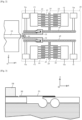
- the figure 2 represents a top view of the component according to the invention comprising its transducer 10 and its electromechanical microsystem 20. This view is in a section plane (O, x, y).
- the electromechanical microsystem 20 comprises two identical actuators and a single piece assembly produced in the first layer comprising the mirror 30 and its two holding springs 31. This assembly is shown in gray on the figure 2 .
- Each actuator consists of two fixed combs 21 and 22 identical and symmetrical with respect to each other and a double movable comb 23 comprising a central beam 24.
- the teeth of the movable comb are intertwined with those of the two fixed combs.
- the central beam 24 is connected to a second beam 25, perpendicular to said beam 24.
- the two beams 25 of the two actuators are parallel to each other.
- Each of these two beams 25 is connected to one of the two retaining springs 31.
- the fixed combs and the movable comb of the actuators are voltage controlled.
- the control voltages of the fixed parts are a few tens of volts.
- the control voltages +V and -V of the figure 2 are +50 V on the first fixed comb and -50 V on the second fixed comb.
- the control voltages Va of the mobile comb are a few volts.
- Controlling a tension actuator causes the translational movement of the mobile comb and, consequently, that of the beam 25 which moves in the direction of its length.
- the movements are represented by white arrows on the figure 2 and the following.
- Each retaining spring 31 comprises a blade in the shape of an elongated rectangle connected to the mirror 30 by a very narrow connection. Given their very thin thickness, the blades have a certain elasticity and can therefore buckle easily. On the figure 2 , the mirror 30 is circular in shape.
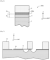
- FIG. 3 represents a side view of the mirror 30 and its retaining springs 31 in the absence of stresses on the interdigitated combs.
- This side view is represented in a section plane (O, x, z).
- the mirror and its springs are in a horizontal plane, parallel to the x axis. No deflection takes place.
- FIG. 4 represents a side view of the mirror and its retaining springs in the presence of stresses from the interdigitated combs.
- the application of control voltages causes the two springs to move as seen in this Figure 4 which abut under the first layer of silicon or silicon nitride placed under the III-V transducer of reference 10.
- This abutment guidance is ensured by a potential difference applied between the second layer and the third thick silicon layer.
- the mirror area is thus positioned under the silicon layer used for optical guidance. If we continue the movement, the leaf springs buckle, causing the mirror to rotate.
- the mirror rotates around the y axis and straightens as seen in the figures 4 and 5 . If the displacements of the two mirrors are different, the mirror rotates around the z axis.
- the transducer is made of III-V material such as indium phosphide or InP in which quantum wells are integrated. This material is then transferred to the silicon substrate.
- the optical guides are manufactured in the first layer 3 of silicon or silicon nitride.
- the second layer 4 of silicon oxide located just under this first layer 3 of silicon or silicon nitride participates in the confinement of the optical mode. In other words, the second layer 4 delimits the optical guide.
- the essential difference with the first embodiment is that the mechanical device 21, 22, 23, 24, 25 for deflecting the light beam is produced in layer III-V.
- mechanical device for deflecting the light beam we mean the actuators 21, 22, 23, 24, 25 of the MEMS device, that is to say the actuators of the mirror 30 and its springs 31.
- the material layer III - V is one-piece.
- This may include the same components as the previous deflection device shown on the figure 2 .
- the components are arranged in the same way but the actuators 21, 22, 23, 24, 25 are made in the III-V material layer. They include, as in the previous case, a symmetrical structure with interdigitated combs connected by beams to an assembly comprising two spring blades 31 supporting a mirror 30 placed in front of the transducer.
- the operation of the device is indicated on the figures 7 And 8 which represent a side view of the mirror and its retaining springs in the absence and presence of stresses on the interdigitated combs.
- This side view is represented in a section plane (O, x, z).
- the mirror and its springs are made from the thin layer of silicon or silicon nitride.
- the mirror orientation mechanism is the same. Apply identical or different control voltages on the actuators, the mirror is oriented along two different axes.
- the abutment guidance of the mirror is ensured by a potential difference applied between the second layer and the substrate.
- the components can be installed on standard wafers of simpler design, already used for the production of III-V components integrated heterogeneously on a standard wafer. If necessary, the silicon substrate can be etched and used to produce parts requiring suitable mechanical properties.
Landscapes
- Physics & Mathematics (AREA)
- Engineering & Computer Science (AREA)
- General Physics & Mathematics (AREA)
- Radar, Positioning & Navigation (AREA)
- Remote Sensing (AREA)
- Computer Networks & Wireless Communication (AREA)
- Optics & Photonics (AREA)
- Electromagnetism (AREA)
- Chemical & Material Sciences (AREA)
- Analytical Chemistry (AREA)
- Microelectronics & Electronic Packaging (AREA)
- Computer Hardware Design (AREA)
- Composite Materials (AREA)
- Materials Engineering (AREA)
- Mechanical Light Control Or Optical Switches (AREA)
- Micromachines (AREA)
- Mechanical Optical Scanning Systems (AREA)
Claims (11)
- Optoelektronisches Bauelement (1), umfassend einen optischen Wandler (10) aus III-V-Halbleitermaterial und ein elektromechanisches Mikrosystem mit optischer Abtastung (20), mit einem Spiegel (30) und Haltefedern (31), wobei der optische Wandler und das elektromechanische Mikrosystem mit optischer Abtastung in einem Wafer hergestellt sind, umfassend, in dieser Reihenfolge, eine Schicht (2) aus III-V-Halbleitermaterial, eine erste Schicht (3) aus Silizium oder Siliziumnitrid mit einer Dicke von weniger als einem Mikrometer, in der mindestens der Spiegel (30) und seine Haltefedern (31) hergestellt sind, eine zweite Schicht (4) aus Siliziumoxid, wobei das optoelektronische Bauelement einen Lichtleiter umfasst, der in der ersten Schicht (3) aus Silizium oder Siliziumnitrid und der zweiten Schicht (4) aus Siliziumoxid enthalten ist.
- Optoelektronisches Bauelement nach Anspruch 1, dadurch gekennzeichnet, dass der gemeinsame Wafer in dieser Reihenfolge die Schicht (2) aus III-V-Halbleitermaterial, die erste Schicht (3) aus Silizium oder Siliziumnitrid, die zweite Schicht (4) aus Siliziumoxid, die dritte Schicht (5) aus Silizium, die vierte Schicht (6) aus Siliziumoxid und ein Substrat (7) aufweist, wobei das elektromechanische Mikrosystem mit optischer Abtastung bewegliche Teile (23, 24, 25) umfasst, die in der dritten Schicht (5) aus Silizium und der vierten Schicht (6) aus Siliziumoxid hergestellt sind.
- Optoelektronisches Bauelement nach Anspruch 2, dadurch gekennzeichnet, dass eine Übertragungsschicht (2bis) aus Siliziumoxid zwischen der Schicht (2) aus III-V-Halbleitermaterial und der ersten Schicht (3) aus Silizium oder Siliziumnitrid angeordnet ist.
- Optoelektronisches Bauelement nach einem der Ansprüche 2 bis 3, dadurch gekennzeichnet, dass die Dicke der zweiten Schicht (4) aus Siliziumoxid zwischen 3 Mikrometern und 4 Mikrometern liegt, die Dicke der dritten Schicht (5) aus Silizium zwischen 10 Mikrometern und 100 Mikrometern liegt und die Dicke der vierten Schicht (6) aus Siliziumoxid zwischen 3 Mikrometern und 4 Mikrometern liegt.
- Optoelektronisches Bauelement nach Anspruch 1, dadurch gekennzeichnet, dass der gemeinsame Wafer in dieser Reihenfolge die Schicht (2) aus III-V-Halbleitermaterial, die erste Schicht (3) aus Silizium oder Siliziumnitrid, die zweite Schicht (4) aus Siliziumoxid und ein Substrat (7) aufweist, wobei das elektromechanische Mikrosystem mit optischer Abtastung bewegliche Teile (23, 24, 25) umfasst, die in der Schicht aus III-V-Halbleitermaterial hergestellt sind.
- Optoelektronisches Bauelement nach Anspruch 5, dadurch gekennzeichnet, dass eine Übertragungsschicht (2bis) aus Siliziumoxid zwischen der Schicht (2) aus III-V-Halbleitermaterial und der ersten Schicht (3) aus Silizium oder Siliziumnitrid angeordnet ist.
- Optoelektronisches Bauelement nach einem der Ansprüche 5 bis 6, dadurch gekennzeichnet, dass die Dicke der zweiten Schicht (4) aus Siliziumoxid zwischen 3 Mikrometern und 4 Mikrometern liegt.
- Optoelektronisches Bauelement nach einem der Ansprüche 2 bis 7, dadurch gekennzeichnet, dass:- die Haltefedern (31) zwei identische ebene Lamellen sind, die im Wesentlichen die Form von länglichen Rechtecken aufweisen, die sich auf beiden Seiten des Spiegels befinden, wobei der Spiegel mit den Lamellen durch eine einzige Befestigung verbunden ist;- die beweglichen Teile aus zwei identischen, zueinander parallelen Trägern (25) bestehen, wobei jeder Träger mit einem Satz von ineinandergreifenden, spannungsgesteuerten Kämmen (23) verbunden ist, um die Bewegung jedes Trägers in eine gleiche gegebene Richtung zu gewährleisten;- jede Lamelle fest mit einem der beiden Träger verbunden ist und sich mit diesem verschiebt, wobei die Verschiebung der Träger ein Knicken der Lamellen im Anschlag an der optischen Führung, ein gemeinsames Knicken der beiden Lamellen, das die Neigung des Spiegels in einer ersten Richtung gewährleistet, ein Differenzialknicken der beiden Lamellen, das die Neigung des Spiegels in einer zweiten Richtung gewährleistet, bewirkt.
- Optoelektronisches Bauelement nach einem der vorhergehenden Ansprüche, dadurch gekennzeichnet, dass der optische Wandler ein Laser ist.
- Optoelektronisches Bauelement nach einem der Ansprüche 1 bis 8, dadurch gekennzeichnet, dass der optische Wandler eine Fotodiode ist.
- Optoelektronisches Bauelement nach einem der vorhergehenden Ansprüche, wobei der Wafer aus Schichten besteht, die jeweils Silizium und die Schicht aus III-V-Halbleitermaterial umfassen.
Applications Claiming Priority (2)
| Application Number | Priority Date | Filing Date | Title |
|---|---|---|---|
| FR1914860A FR3105450B1 (fr) | 2019-12-19 | 2019-12-19 | Composant optoelectronique comprenant sur un substrat unique un transducteur optique en materiau semi-conducteur iii-v et un microsysteme electromecanique a balayage optique |
| PCT/EP2020/087289 WO2021123359A1 (fr) | 2019-12-19 | 2020-12-18 | Composant optoélectronique comprenant sur un substrat unique un transducteur optique en matériau semi-conducteur iii-v et un microsystème électromécanique à balayage optique |
Publications (2)
| Publication Number | Publication Date |
|---|---|
| EP4078219A1 EP4078219A1 (de) | 2022-10-26 |
| EP4078219B1 true EP4078219B1 (de) | 2024-01-03 |
Family
ID=70918504
Family Applications (1)
| Application Number | Title | Priority Date | Filing Date |
|---|---|---|---|
| EP20835812.7A Active EP4078219B1 (de) | 2019-12-19 | 2020-12-18 | Optoelektronisches bauelement, das auf einem einzigen substrat einen optischen wandler aus einem halbleitermaterial iii-v und ein optisch abtastendes mikroelektromechanisches system umfasst |
Country Status (4)
| Country | Link |
|---|---|
| US (1) | US12219878B2 (de) |
| EP (1) | EP4078219B1 (de) |
| FR (1) | FR3105450B1 (de) |
| WO (1) | WO2021123359A1 (de) |
Family Cites Families (7)
| Publication number | Priority date | Publication date | Assignee | Title |
|---|---|---|---|---|
| US6002507A (en) * | 1998-12-01 | 1999-12-14 | Xerox Corpoation | Method and apparatus for an integrated laser beam scanner |
| DE102013220787A1 (de) * | 2013-10-15 | 2015-04-16 | Robert Bosch Gmbh | Mikromechanisches Bauelement mit integrierter Photodiode und Mikroprojektor |
| US10203399B2 (en) | 2013-11-12 | 2019-02-12 | Big Sky Financial Corporation | Methods and apparatus for array based LiDAR systems with reduced interference |
| DE102015225863A1 (de) | 2015-12-18 | 2017-06-22 | Robert Bosch Gmbh | Optische phasengesteuerte Anordnung und LiDAR System |
| US11723762B2 (en) | 2016-01-31 | 2023-08-15 | Velodyne Lidar, Inc. | LIDAR based 3-D imaging with far-field illumination overlap |
| CN109154661A (zh) | 2016-03-19 | 2019-01-04 | 威力登激光雷达有限公司 | 用于基于lidar的3-d成像的集成照射和检测 |
| KR102559580B1 (ko) | 2016-08-17 | 2023-07-25 | 삼성전자주식회사 | 광 조향용 OPA, 및 그 OPA를 구비한 LiDAR 시스템 |
-
2019
- 2019-12-19 FR FR1914860A patent/FR3105450B1/fr active Active
-
2020
- 2020-12-18 EP EP20835812.7A patent/EP4078219B1/de active Active
- 2020-12-18 WO PCT/EP2020/087289 patent/WO2021123359A1/fr not_active Ceased
- 2020-12-18 US US17/787,326 patent/US12219878B2/en active Active
Also Published As
| Publication number | Publication date |
|---|---|
| WO2021123359A1 (fr) | 2021-06-24 |
| EP4078219A1 (de) | 2022-10-26 |
| FR3105450B1 (fr) | 2023-08-25 |
| FR3105450A1 (fr) | 2021-06-25 |
| US12219878B2 (en) | 2025-02-04 |
| US20230019436A1 (en) | 2023-01-19 |
Similar Documents
| Publication | Publication Date | Title |
|---|---|---|
| EP1364190B1 (de) | Optoelektronische vorrichtung zur wellenlängenfilterung durch kavitätenkopplung | |
| US7339738B1 (en) | Nanomechanical near-field grating apparatus and acceleration sensor formed therefrom | |
| TW202129302A (zh) | 用於光達應用之微機電系統相位陣列 | |
| EP0218546B1 (de) | Vorrichtung für die Mikropositionierung | |
| WO2020142088A1 (en) | Micromachined mirror assembly having reflective layers on both sides | |
| EP3926392B1 (de) | Optisches gerät und herstellungsprozess | |
| EP1259847B1 (de) | Optoelektronische halbleitervorrichtung mit elektrisch modulierbarer übertragungsfunktion | |
| EP0742459B1 (de) | Optomechanischer Mikro-Strahlablenker unter Verwendung der Verschiebung von Mikrolinsen | |
| EP4078219B1 (de) | Optoelektronisches bauelement, das auf einem einzigen substrat einen optischen wandler aus einem halbleitermaterial iii-v und ein optisch abtastendes mikroelektromechanisches system umfasst | |
| EP3764148B1 (de) | Scanner mit optischer netzeinheit mit mobiler phasensteuerung | |
| EP1257027A1 (de) | Optische Vorrichtung mit mehreren Resonatoren mit unterschiedlichen Resonatorlänge und wellenlänge | |
| EP3514614B1 (de) | Optische vorrichtung | |
| EP4075182B1 (de) | Optischer scanner | |
| EP3913393B1 (de) | Verbesserte detektionsvorrichtung und entsprechendes lidar-system | |
| EP3933484A1 (de) | Optischer scanner | |
| EP2473824B1 (de) | Feldkompensiertes interferometer | |
| EP4298460A1 (de) | Optoelektronischer emitter mit phasengesteuerter gruppenantenne mit aufgeweiteter laserquelle | |
| EP3933483A1 (de) | Optischer scanner | |
| US11958738B2 (en) | Dual-layer micro-ribbon MEMS light modulator | |
| EP4553561A1 (de) | Reflektorvorrichtung mit einem detektor und verfahren dafür | |
| WO2009062957A1 (fr) | Stabilisation optique d'un emetteur laser | |
| EP3563186B1 (de) | Kollimator | |
| WO2023110684A1 (fr) | Emetteur optoelectronique a antenne reseau a commande de phase ou chaque antenne optique presente une large surface d'emission | |
| FR3121760A1 (fr) | Dispositif reflecteur destine a emettre une pluralite de faisceaux reflechis a partir d’un unique faisceau lumineux principal | |
| FR2865548A1 (fr) | Dispositif permettant de deplacer le point objet d'une source optique et systeme permettant de deplacer le point image d'une source optique |
Legal Events
| Date | Code | Title | Description |
|---|---|---|---|
| STAA | Information on the status of an ep patent application or granted ep patent |
Free format text: STATUS: UNKNOWN |
|
| STAA | Information on the status of an ep patent application or granted ep patent |
Free format text: STATUS: THE INTERNATIONAL PUBLICATION HAS BEEN MADE |
|
| PUAI | Public reference made under article 153(3) epc to a published international application that has entered the european phase |
Free format text: ORIGINAL CODE: 0009012 |
|
| STAA | Information on the status of an ep patent application or granted ep patent |
Free format text: STATUS: REQUEST FOR EXAMINATION WAS MADE |
|
| 17P | Request for examination filed |
Effective date: 20220617 |
|
| AK | Designated contracting states |
Kind code of ref document: A1 Designated state(s): AL AT BE BG CH CY CZ DE DK EE ES FI FR GB GR HR HU IE IS IT LI LT LU LV MC MK MT NL NO PL PT RO RS SE SI SK SM TR |
|
| DAV | Request for validation of the european patent (deleted) | ||
| DAX | Request for extension of the european patent (deleted) | ||
| GRAP | Despatch of communication of intention to grant a patent |
Free format text: ORIGINAL CODE: EPIDOSNIGR1 |
|
| STAA | Information on the status of an ep patent application or granted ep patent |
Free format text: STATUS: GRANT OF PATENT IS INTENDED |
|
| INTG | Intention to grant announced |
Effective date: 20230725 |
|
| GRAS | Grant fee paid |
Free format text: ORIGINAL CODE: EPIDOSNIGR3 |
|
| GRAA | (expected) grant |
Free format text: ORIGINAL CODE: 0009210 |
|
| STAA | Information on the status of an ep patent application or granted ep patent |
Free format text: STATUS: THE PATENT HAS BEEN GRANTED |
|
| RAP3 | Party data changed (applicant data changed or rights of an application transferred) |
Owner name: THALES |
|
| AK | Designated contracting states |
Kind code of ref document: B1 Designated state(s): AL AT BE BG CH CY CZ DE DK EE ES FI FR GB GR HR HU IE IS IT LI LT LU LV MC MK MT NL NO PL PT RO RS SE SI SK SM TR |
|
| REG | Reference to a national code |
Ref country code: GB Ref legal event code: FG4D Free format text: NOT ENGLISH |
|
| REG | Reference to a national code |
Ref country code: CH Ref legal event code: EP |
|
| REG | Reference to a national code |
Ref country code: DE Ref legal event code: R096 Ref document number: 602020024015 Country of ref document: DE |
|
| REG | Reference to a national code |
Ref country code: IE Ref legal event code: FG4D Free format text: LANGUAGE OF EP DOCUMENT: FRENCH |
|
| REG | Reference to a national code |
Ref country code: LT Ref legal event code: MG9D |
|
| PG25 | Lapsed in a contracting state [announced via postgrant information from national office to epo] |
Ref country code: ES Free format text: LAPSE BECAUSE OF FAILURE TO SUBMIT A TRANSLATION OF THE DESCRIPTION OR TO PAY THE FEE WITHIN THE PRESCRIBED TIME-LIMIT Effective date: 20240103 |
|
| PG25 | Lapsed in a contracting state [announced via postgrant information from national office to epo] |
Ref country code: ES Free format text: LAPSE BECAUSE OF FAILURE TO SUBMIT A TRANSLATION OF THE DESCRIPTION OR TO PAY THE FEE WITHIN THE PRESCRIBED TIME-LIMIT Effective date: 20240103 |
|
| REG | Reference to a national code |
Ref country code: NL Ref legal event code: MP Effective date: 20240103 |
|
| REG | Reference to a national code |
Ref country code: AT Ref legal event code: MK05 Ref document number: 1647341 Country of ref document: AT Kind code of ref document: T Effective date: 20240103 |
|
| PG25 | Lapsed in a contracting state [announced via postgrant information from national office to epo] |
Ref country code: NL Free format text: LAPSE BECAUSE OF FAILURE TO SUBMIT A TRANSLATION OF THE DESCRIPTION OR TO PAY THE FEE WITHIN THE PRESCRIBED TIME-LIMIT Effective date: 20240103 |
|
| PG25 | Lapsed in a contracting state [announced via postgrant information from national office to epo] |
Ref country code: NL Free format text: LAPSE BECAUSE OF FAILURE TO SUBMIT A TRANSLATION OF THE DESCRIPTION OR TO PAY THE FEE WITHIN THE PRESCRIBED TIME-LIMIT Effective date: 20240103 |
|
| PG25 | Lapsed in a contracting state [announced via postgrant information from national office to epo] |
Ref country code: IS Free format text: LAPSE BECAUSE OF FAILURE TO SUBMIT A TRANSLATION OF THE DESCRIPTION OR TO PAY THE FEE WITHIN THE PRESCRIBED TIME-LIMIT Effective date: 20240503 |
|
| PG25 | Lapsed in a contracting state [announced via postgrant information from national office to epo] |
Ref country code: LT Free format text: LAPSE BECAUSE OF FAILURE TO SUBMIT A TRANSLATION OF THE DESCRIPTION OR TO PAY THE FEE WITHIN THE PRESCRIBED TIME-LIMIT Effective date: 20240103 |
|
| PG25 | Lapsed in a contracting state [announced via postgrant information from national office to epo] |
Ref country code: GR Free format text: LAPSE BECAUSE OF FAILURE TO SUBMIT A TRANSLATION OF THE DESCRIPTION OR TO PAY THE FEE WITHIN THE PRESCRIBED TIME-LIMIT Effective date: 20240404 |
|
| PG25 | Lapsed in a contracting state [announced via postgrant information from national office to epo] |
Ref country code: HR Free format text: LAPSE BECAUSE OF FAILURE TO SUBMIT A TRANSLATION OF THE DESCRIPTION OR TO PAY THE FEE WITHIN THE PRESCRIBED TIME-LIMIT Effective date: 20240103 Ref country code: RS Free format text: LAPSE BECAUSE OF FAILURE TO SUBMIT A TRANSLATION OF THE DESCRIPTION OR TO PAY THE FEE WITHIN THE PRESCRIBED TIME-LIMIT Effective date: 20240403 |
|
| PG25 | Lapsed in a contracting state [announced via postgrant information from national office to epo] |
Ref country code: CZ Free format text: LAPSE BECAUSE OF FAILURE TO SUBMIT A TRANSLATION OF THE DESCRIPTION OR TO PAY THE FEE WITHIN THE PRESCRIBED TIME-LIMIT Effective date: 20240103 Ref country code: AT Free format text: LAPSE BECAUSE OF FAILURE TO SUBMIT A TRANSLATION OF THE DESCRIPTION OR TO PAY THE FEE WITHIN THE PRESCRIBED TIME-LIMIT Effective date: 20240103 |
|
| PG25 | Lapsed in a contracting state [announced via postgrant information from national office to epo] |
Ref country code: RS Free format text: LAPSE BECAUSE OF FAILURE TO SUBMIT A TRANSLATION OF THE DESCRIPTION OR TO PAY THE FEE WITHIN THE PRESCRIBED TIME-LIMIT Effective date: 20240403 Ref country code: NO Free format text: LAPSE BECAUSE OF FAILURE TO SUBMIT A TRANSLATION OF THE DESCRIPTION OR TO PAY THE FEE WITHIN THE PRESCRIBED TIME-LIMIT Effective date: 20240403 Ref country code: LT Free format text: LAPSE BECAUSE OF FAILURE TO SUBMIT A TRANSLATION OF THE DESCRIPTION OR TO PAY THE FEE WITHIN THE PRESCRIBED TIME-LIMIT Effective date: 20240103 Ref country code: IS Free format text: LAPSE BECAUSE OF FAILURE TO SUBMIT A TRANSLATION OF THE DESCRIPTION OR TO PAY THE FEE WITHIN THE PRESCRIBED TIME-LIMIT Effective date: 20240503 Ref country code: HR Free format text: LAPSE BECAUSE OF FAILURE TO SUBMIT A TRANSLATION OF THE DESCRIPTION OR TO PAY THE FEE WITHIN THE PRESCRIBED TIME-LIMIT Effective date: 20240103 Ref country code: GR Free format text: LAPSE BECAUSE OF FAILURE TO SUBMIT A TRANSLATION OF THE DESCRIPTION OR TO PAY THE FEE WITHIN THE PRESCRIBED TIME-LIMIT Effective date: 20240404 Ref country code: CZ Free format text: LAPSE BECAUSE OF FAILURE TO SUBMIT A TRANSLATION OF THE DESCRIPTION OR TO PAY THE FEE WITHIN THE PRESCRIBED TIME-LIMIT Effective date: 20240103 Ref country code: BG Free format text: LAPSE BECAUSE OF FAILURE TO SUBMIT A TRANSLATION OF THE DESCRIPTION OR TO PAY THE FEE WITHIN THE PRESCRIBED TIME-LIMIT Effective date: 20240103 Ref country code: AT Free format text: LAPSE BECAUSE OF FAILURE TO SUBMIT A TRANSLATION OF THE DESCRIPTION OR TO PAY THE FEE WITHIN THE PRESCRIBED TIME-LIMIT Effective date: 20240103 |
|
| PG25 | Lapsed in a contracting state [announced via postgrant information from national office to epo] |
Ref country code: PL Free format text: LAPSE BECAUSE OF FAILURE TO SUBMIT A TRANSLATION OF THE DESCRIPTION OR TO PAY THE FEE WITHIN THE PRESCRIBED TIME-LIMIT Effective date: 20240103 Ref country code: PT Free format text: LAPSE BECAUSE OF FAILURE TO SUBMIT A TRANSLATION OF THE DESCRIPTION OR TO PAY THE FEE WITHIN THE PRESCRIBED TIME-LIMIT Effective date: 20240503 |
|
| PG25 | Lapsed in a contracting state [announced via postgrant information from national office to epo] |
Ref country code: SE Free format text: LAPSE BECAUSE OF FAILURE TO SUBMIT A TRANSLATION OF THE DESCRIPTION OR TO PAY THE FEE WITHIN THE PRESCRIBED TIME-LIMIT Effective date: 20240103 Ref country code: PT Free format text: LAPSE BECAUSE OF FAILURE TO SUBMIT A TRANSLATION OF THE DESCRIPTION OR TO PAY THE FEE WITHIN THE PRESCRIBED TIME-LIMIT Effective date: 20240503 Ref country code: PL Free format text: LAPSE BECAUSE OF FAILURE TO SUBMIT A TRANSLATION OF THE DESCRIPTION OR TO PAY THE FEE WITHIN THE PRESCRIBED TIME-LIMIT Effective date: 20240103 Ref country code: LV Free format text: LAPSE BECAUSE OF FAILURE TO SUBMIT A TRANSLATION OF THE DESCRIPTION OR TO PAY THE FEE WITHIN THE PRESCRIBED TIME-LIMIT Effective date: 20240103 |
|
| REG | Reference to a national code |
Ref country code: DE Ref legal event code: R097 Ref document number: 602020024015 Country of ref document: DE |
|
| PG25 | Lapsed in a contracting state [announced via postgrant information from national office to epo] |
Ref country code: DK Free format text: LAPSE BECAUSE OF FAILURE TO SUBMIT A TRANSLATION OF THE DESCRIPTION OR TO PAY THE FEE WITHIN THE PRESCRIBED TIME-LIMIT Effective date: 20240103 |
|
| PG25 | Lapsed in a contracting state [announced via postgrant information from national office to epo] |
Ref country code: SM Free format text: LAPSE BECAUSE OF FAILURE TO SUBMIT A TRANSLATION OF THE DESCRIPTION OR TO PAY THE FEE WITHIN THE PRESCRIBED TIME-LIMIT Effective date: 20240103 |
|
| PG25 | Lapsed in a contracting state [announced via postgrant information from national office to epo] |
Ref country code: EE Free format text: LAPSE BECAUSE OF FAILURE TO SUBMIT A TRANSLATION OF THE DESCRIPTION OR TO PAY THE FEE WITHIN THE PRESCRIBED TIME-LIMIT Effective date: 20240103 |
|
| PG25 | Lapsed in a contracting state [announced via postgrant information from national office to epo] |
Ref country code: SK Free format text: LAPSE BECAUSE OF FAILURE TO SUBMIT A TRANSLATION OF THE DESCRIPTION OR TO PAY THE FEE WITHIN THE PRESCRIBED TIME-LIMIT Effective date: 20240103 |
|
| PG25 | Lapsed in a contracting state [announced via postgrant information from national office to epo] |
Ref country code: SM Free format text: LAPSE BECAUSE OF FAILURE TO SUBMIT A TRANSLATION OF THE DESCRIPTION OR TO PAY THE FEE WITHIN THE PRESCRIBED TIME-LIMIT Effective date: 20240103 Ref country code: SK Free format text: LAPSE BECAUSE OF FAILURE TO SUBMIT A TRANSLATION OF THE DESCRIPTION OR TO PAY THE FEE WITHIN THE PRESCRIBED TIME-LIMIT Effective date: 20240103 Ref country code: RO Free format text: LAPSE BECAUSE OF FAILURE TO SUBMIT A TRANSLATION OF THE DESCRIPTION OR TO PAY THE FEE WITHIN THE PRESCRIBED TIME-LIMIT Effective date: 20240103 Ref country code: EE Free format text: LAPSE BECAUSE OF FAILURE TO SUBMIT A TRANSLATION OF THE DESCRIPTION OR TO PAY THE FEE WITHIN THE PRESCRIBED TIME-LIMIT Effective date: 20240103 Ref country code: DK Free format text: LAPSE BECAUSE OF FAILURE TO SUBMIT A TRANSLATION OF THE DESCRIPTION OR TO PAY THE FEE WITHIN THE PRESCRIBED TIME-LIMIT Effective date: 20240103 |
|
| PLBE | No opposition filed within time limit |
Free format text: ORIGINAL CODE: 0009261 |
|
| STAA | Information on the status of an ep patent application or granted ep patent |
Free format text: STATUS: NO OPPOSITION FILED WITHIN TIME LIMIT |
|
| PG25 | Lapsed in a contracting state [announced via postgrant information from national office to epo] |
Ref country code: IT Free format text: LAPSE BECAUSE OF FAILURE TO SUBMIT A TRANSLATION OF THE DESCRIPTION OR TO PAY THE FEE WITHIN THE PRESCRIBED TIME-LIMIT Effective date: 20240103 |
|
| 26N | No opposition filed |
Effective date: 20241007 |
|
| PG25 | Lapsed in a contracting state [announced via postgrant information from national office to epo] |
Ref country code: IT Free format text: LAPSE BECAUSE OF FAILURE TO SUBMIT A TRANSLATION OF THE DESCRIPTION OR TO PAY THE FEE WITHIN THE PRESCRIBED TIME-LIMIT Effective date: 20240103 |
|
| PG25 | Lapsed in a contracting state [announced via postgrant information from national office to epo] |
Ref country code: SI Free format text: LAPSE BECAUSE OF FAILURE TO SUBMIT A TRANSLATION OF THE DESCRIPTION OR TO PAY THE FEE WITHIN THE PRESCRIBED TIME-LIMIT Effective date: 20240103 |
|
| PG25 | Lapsed in a contracting state [announced via postgrant information from national office to epo] |
Ref country code: MC Free format text: LAPSE BECAUSE OF FAILURE TO SUBMIT A TRANSLATION OF THE DESCRIPTION OR TO PAY THE FEE WITHIN THE PRESCRIBED TIME-LIMIT Effective date: 20240103 |
|
| REG | Reference to a national code |
Ref country code: CH Ref legal event code: PL |
|
| PG25 | Lapsed in a contracting state [announced via postgrant information from national office to epo] |
Ref country code: LU Free format text: LAPSE BECAUSE OF NON-PAYMENT OF DUE FEES Effective date: 20241218 |
|
| GBPC | Gb: european patent ceased through non-payment of renewal fee |
Effective date: 20241218 |
|
| PG25 | Lapsed in a contracting state [announced via postgrant information from national office to epo] |
Ref country code: FI Free format text: LAPSE BECAUSE OF FAILURE TO SUBMIT A TRANSLATION OF THE DESCRIPTION OR TO PAY THE FEE WITHIN THE PRESCRIBED TIME-LIMIT Effective date: 20240103 |
|
| REG | Reference to a national code |
Ref country code: BE Ref legal event code: MM Effective date: 20241231 |
|
| PG25 | Lapsed in a contracting state [announced via postgrant information from national office to epo] |
Ref country code: BE Free format text: LAPSE BECAUSE OF NON-PAYMENT OF DUE FEES Effective date: 20241231 Ref country code: GB Free format text: LAPSE BECAUSE OF NON-PAYMENT OF DUE FEES Effective date: 20241218 |
|
| PG25 | Lapsed in a contracting state [announced via postgrant information from national office to epo] |
Ref country code: CH Free format text: LAPSE BECAUSE OF NON-PAYMENT OF DUE FEES Effective date: 20241231 |
|
| PG25 | Lapsed in a contracting state [announced via postgrant information from national office to epo] |
Ref country code: IE Free format text: LAPSE BECAUSE OF NON-PAYMENT OF DUE FEES Effective date: 20241218 |
|
| PGFP | Annual fee paid to national office [announced via postgrant information from national office to epo] |
Ref country code: DE Payment date: 20251119 Year of fee payment: 6 |
|
| PGFP | Annual fee paid to national office [announced via postgrant information from national office to epo] |
Ref country code: FR Payment date: 20251124 Year of fee payment: 6 |