EP3936887A1 - Kohärentes lidar-system mit verbessertem signal-rausch-verhältnis - Google Patents
Kohärentes lidar-system mit verbessertem signal-rausch-verhältnis Download PDFInfo
- Publication number
- EP3936887A1 EP3936887A1 EP21180453.9A EP21180453A EP3936887A1 EP 3936887 A1 EP3936887 A1 EP 3936887A1 EP 21180453 A EP21180453 A EP 21180453A EP 3936887 A1 EP3936887 A1 EP 3936887A1
- Authority
- EP
- European Patent Office
- Prior art keywords
- pixel
- intensity
- optical
- pix
- reference beam
- Prior art date
- Legal status (The legal status is an assumption and is not a legal conclusion. Google has not performed a legal analysis and makes no representation as to the accuracy of the status listed.)
- Granted
Links
Images







Classifications
-
- G—PHYSICS
- G01—MEASURING; TESTING
- G01S—RADIO DIRECTION-FINDING; RADIO NAVIGATION; DETERMINING DISTANCE OR VELOCITY BY USE OF RADIO WAVES; LOCATING OR PRESENCE-DETECTING BY USE OF THE REFLECTION OR RERADIATION OF RADIO WAVES; ANALOGOUS ARRANGEMENTS USING OTHER WAVES
- G01S7/00—Details of systems according to groups G01S13/00, G01S15/00, G01S17/00
- G01S7/48—Details of systems according to groups G01S13/00, G01S15/00, G01S17/00 of systems according to group G01S17/00
- G01S7/481—Constructional features, e.g. arrangements of optical elements
- G01S7/4816—Constructional features, e.g. arrangements of optical elements of receivers alone
-
- G—PHYSICS
- G01—MEASURING; TESTING
- G01S—RADIO DIRECTION-FINDING; RADIO NAVIGATION; DETERMINING DISTANCE OR VELOCITY BY USE OF RADIO WAVES; LOCATING OR PRESENCE-DETECTING BY USE OF THE REFLECTION OR RERADIATION OF RADIO WAVES; ANALOGOUS ARRANGEMENTS USING OTHER WAVES
- G01S17/00—Systems using the reflection or reradiation of electromagnetic waves other than radio waves, e.g. lidar systems
- G01S17/88—Lidar systems specially adapted for specific applications
- G01S17/89—Lidar systems specially adapted for specific applications for mapping or imaging
-
- G—PHYSICS
- G01—MEASURING; TESTING
- G01S—RADIO DIRECTION-FINDING; RADIO NAVIGATION; DETERMINING DISTANCE OR VELOCITY BY USE OF RADIO WAVES; LOCATING OR PRESENCE-DETECTING BY USE OF THE REFLECTION OR RERADIATION OF RADIO WAVES; ANALOGOUS ARRANGEMENTS USING OTHER WAVES
- G01S17/00—Systems using the reflection or reradiation of electromagnetic waves other than radio waves, e.g. lidar systems
- G01S17/88—Lidar systems specially adapted for specific applications
- G01S17/89—Lidar systems specially adapted for specific applications for mapping or imaging
- G01S17/894—Three-dimensional [3D] imaging with simultaneous measurement of time-of-flight at a two-dimensional [2D] array of receiver pixels, e.g. time-of-flight cameras or flash lidar
-
- G—PHYSICS
- G01—MEASURING; TESTING
- G01S—RADIO DIRECTION-FINDING; RADIO NAVIGATION; DETERMINING DISTANCE OR VELOCITY BY USE OF RADIO WAVES; LOCATING OR PRESENCE-DETECTING BY USE OF THE REFLECTION OR RERADIATION OF RADIO WAVES; ANALOGOUS ARRANGEMENTS USING OTHER WAVES
- G01S7/00—Details of systems according to groups G01S13/00, G01S15/00, G01S17/00
- G01S7/48—Details of systems according to groups G01S13/00, G01S15/00, G01S17/00 of systems according to group G01S17/00
- G01S7/491—Details of non-pulse systems
- G01S7/4911—Transmitters
-
- G—PHYSICS
- G01—MEASURING; TESTING
- G01S—RADIO DIRECTION-FINDING; RADIO NAVIGATION; DETERMINING DISTANCE OR VELOCITY BY USE OF RADIO WAVES; LOCATING OR PRESENCE-DETECTING BY USE OF THE REFLECTION OR RERADIATION OF RADIO WAVES; ANALOGOUS ARRANGEMENTS USING OTHER WAVES
- G01S7/00—Details of systems according to groups G01S13/00, G01S15/00, G01S17/00
- G01S7/48—Details of systems according to groups G01S13/00, G01S15/00, G01S17/00 of systems according to group G01S17/00
- G01S7/491—Details of non-pulse systems
- G01S7/4912—Receivers
- G01S7/4918—Controlling received signal intensity, gain or exposure of sensor
-
- G—PHYSICS
- G01—MEASURING; TESTING
- G01S—RADIO DIRECTION-FINDING; RADIO NAVIGATION; DETERMINING DISTANCE OR VELOCITY BY USE OF RADIO WAVES; LOCATING OR PRESENCE-DETECTING BY USE OF THE REFLECTION OR RERADIATION OF RADIO WAVES; ANALOGOUS ARRANGEMENTS USING OTHER WAVES
- G01S7/00—Details of systems according to groups G01S13/00, G01S15/00, G01S17/00
- G01S7/48—Details of systems according to groups G01S13/00, G01S15/00, G01S17/00 of systems according to group G01S17/00
- G01S7/491—Details of non-pulse systems
- G01S7/493—Extracting wanted echo signals
Definitions
- the present invention relates to the field of imaging by coherent Lidar and more particularly to Lidar imaging systems having improved detection.
- a coherent Lidar system is a system in which a part of the coherent illumination light source is deflected in order to be used as an amplifier of the signal backscattered by the scene once the latter is illuminated by the rest of the non-deflected beam.
- a coherent lidar comprises a coherent source, typically a laser, which emits a coherent light wave (IR, visible or near UV domain), an emission device which makes it possible to illuminate a volume of space, and a reception device , which collects a fraction of the light wave backscattered by a target T.
- the Doppler frequency shift of the backscattered wave is a function of the radial velocity v of the target T:
- the interference of these two waves is detected by a photo-detector PD, and the electrical signal at the output of the detector has an oscillating term called the beat signal Sb, in addition to terms proportional to the received power and to the oscillator power. local.
- This signal is digitized and information on the speed of the target T is extracted.
- FMCW Frequency Modulated Continuous Wave
- the two channels which interfere on the photo-detector produce beats whose frequency is proportional to the delay between the two channels, therefore to the distance.
- the distance resolution is ⁇ z ⁇ vs 2 B . It is also possible to measure ⁇ R by spectral analysis by Fourier transform of the beat signal.
- the interference signal contains a generally large and unnecessary DC component, which is suppressed by an electronic high-pass filter if the photo-receiver is a photodiode.
- an electronic high-pass filter if the photo-receiver is a photodiode.
- the detection circuit makes it possible to differentiate the two photo-currents, thus to suppress the DC (common mode) and to detect the AC part (beat signal).
- the AC part is usually amplified externally by a trans-impedance amplifier (TIA) before being processed by external electronics, for example an oscilloscope, to measure the frequency.
- TIA trans-impedance amplifier
- the FMCW lidar technique is an optical heterodyne measurement technique (i.e. involving several optical frequencies).
- the technique is very insensitive to stray ambient light such as sunlight.
- the lidar scans the scene sequentially using a scanning device (image of the “rolling shutter” type).
- the Aflatouni publication “Nano photonic coherent imager” (2015, Optics Express vol. 23 n°4, 5117 ), which also uses the FMCW technique, describes a device in which the whole scene is illuminated simultaneously by the laser beam which has been made divergent, and the photo-detection is done in parallel for the whole scene.
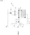
- the laser source Las is frequency modulated by a modulator Mod
- the object channel illuminates the object to be analyzed O
- a lens L forms the image of the object on a coherent imager IC produced in integrated optics, more precisely on a matrix of 4x4 optical coupling gratings Res.
- Each Res grating sends the coupled light to a side-coupled PD photodiode located outside the image, via a waveguide (see picture 3 ).
- the reference channel local oscillator LO wave
- the reference channel is sent directly to the photodiodes by an optical fiber Fib and by a network of waveguides and Y junctions.
- the conversion of the photocurrent into voltage is carried out by a trans- TIA impedance for each of the 16 photodiodes.
- Electronic filtering and signal processing is performed off-chip in an electronic detection system SED.
- An object of the present invention is to remedy the aforementioned drawbacks by proposing a coherent Lidar imaging system allowing the parallel acquisition of a large number of pixels and for each pixel an improved detection at the level of the management of the saturation of the photo-detector and the signal-to-noise ratio.
- the signal-to-noise ratio for a pixel corresponds to the ratio of the modulated intensity integrated over a given time over a square root of the total intensity integrated over the same time, the signal-to-noise ratio being determined from pixel signal-to-noise ratios.
- the optimization criterion further comprises obtaining, for each pixel, a total intensity or a modulated intensity that is also improved.
- the optimization criterion further comprises obtaining a dispersion of the values of reduced pixel signal-to-noise ratio.
- the reference beam propagates in free space
- the second optical device comprising a recombination optical device, called a combiner, configured to superimpose the reference beam and the image beam reflected by the scene
- the splitter and the second optical device being configured to form a virtual or real intermediate image of the reference beam in a plane perpendicular to said optical axis, called intermediate image plane, said intermediate plane being arranged so as to generate flat tone fringes obtained by interference, on each illuminated pixel, between the pixel reference beam and the pixel image beam
- the intensity modulator being an electrically controllable matrix component positioned on the optical path of the reference beam downstream of the splitter and upstream of the second optical device.
- the second optical device further comprises an intermediate optical system suitable for forming said intermediate image and arranged after the splitter and the matrix component and before the combiner, the intermediate optical system in combination with the imaging optical system being further arranged to form an image of the matrix component on the detection device.
- the separator is an electrically adjustable Fabry-Perot filter.
- the matrix component is a liquid crystal modulator.
- the combiner has a second identical modulable transmittance for all the pixels, the processing unit being further configured to apply a second transmittance value via said feedback loop and according to said optimization criterion.
- the integrated intensity modulator is a resonant ring.
- the splitter, the second optical device and the detector are produced on the same substrate, the splitter comprising an integrated optical circuit which is subdivided, via a modular Y junction, into, on the one hand, at least one waveguide comprising at least one diffraction grating, called object grating, the at least one object grating being configured to decouple part of the laser beam from the plane of the integrated optical circuit so as to form the object beam, and on the other hand a guide wave without grating guiding the reference beam to the detector.
- the pixel coupler is a modular directional coupler, so as to vary a ratio between the pixel reference beam and pixel image beam, the processing unit being further configured to apply a ratio value via said d loop enslavement and according to said optimization criterion.
- the method further comprises a step C′ consisting in applying a ratio value between the pixel reference beam and pixel image beam, said ratio value being determined by said servo loop.
- the coherent Lidar imaging system according to the invention is based on lidar architectures described in the patent applications FR2000408 and FR2005186 , unpublished at the filing date of this application. These two types of coherent Lidar system architectures allow the acquisition of a large number of pixels in parallel. These architectures include a matrix detector (or imager) in which each pixel includes a photoreceptor.
- the lidar system described in the document FR2000408 is based on free-space propagation of the reference beam (local oscillator) and will be referred to as a free-space lidar system
- the lidar described in document FR2005186 is based on guided optical propagation of the reference beam, and will be referred to as an integrated lidar system.
- the architecture of the lidar system in free space 40 is recalled figure 4 .
- the lidar is of the FMCW type and includes a laser source SL configured to emit laser radiation L with a temporally modulated optical frequency FL.
- the optical frequency is modulated by a periodic ramp of excursion B and of duration T, and the coherence length of the laser radiation is at least twice greater than the maximum predetermined distance zmax between the scene to be observed Obj and the lidar 40.
- the lidar 40 also comprises an optical device DS, called a splitter, adapted to spatially separate the laser radiation L into a beam called the reference beam Lref and into a beam called the object beam Lo directed towards the scene to be observed Obj and a recombination optical device DR, called combiner, adapted to spatially superimpose the reference beam Lref on the beam reflected by the scene Lo,r, so as to form a recombined beam. Lrec.
- an optical device DS called a splitter
- DR recombination optical device
- the lidar 40 also comprises a matrix detection device 41 and an optical imaging system Im with optical axis AO (diaphragm Diaph) which produces an image of the scene by imaging the beam reflected by the scene Lo,r on the detector 41
- the scene being typically at infinity, the detector 41 is placed substantially in the focal plane of the optics Im.
- the matrix detector 41 comprises a matrix of pixels Pij, each pixel comprising a photo-detector component PD(i,j).
- the photo-detector PD detects a flux of photons, which it transforms into a flux of electrons.
- the optical devices DS and DR and the imaging optical system Im are configured so that each pixel Pij of the detector receives a portion of the image beam coming from the scene called Lo,r/pix and a portion of the reference called Lref/pix, and that the portions are spatially superimposed in a coherent manner on each pixel.
- the devices DS and DR are configured, for example with the addition of additional optics SI (not shown), to transport the reference beam coherently from the laser source to an intermediate image plane PI, perpendicular to the optical axis AO of the imaging optical system Im, so as to produce a coherent reference source (virtual or real) with the reflected beam.
- the intermediate plane PI is located close to the optical imaging system, so as to generate flat tint fringes, obtained by interference between the portion of the reflected beam detected Lo,r/pix and the portion of the reference beam detected Lref/ pix, on each illuminated Pij pixel.
- the beam portion illuminating a pixel is assimilated to the beam portion detected by the photo-detector of this pixel.
- This flat tint condition implies that, on each pixel Pij, an axis of propagation of the portion Lo,r/pix of the reflected beam is collinear or substantially collinear with an axis of propagation of the portion Lref/pix of the reference beam.
- the devices DS, DR and SI are therefore configured to form a virtual or real intermediate image PS of the reference beam in the intermediate image plane PI, the plane PI being arranged so as to generate flat tint fringes, obtained by interference between the portions, on each illuminated pixel.
- the coherent lidar imaging system 40 further comprising at least one electronic processing circuit configured to calculate, for each pixel Pij, a frequency F(i,j) of the beat of the portion of the image beam with the portion of the reference beam illuminating the pixel.
- the lidar 40 comprises a processing unit UT connected to the laser source and to the detector 41, and configured to determine a distance of points of the scene imaged on the pixels, from the beat frequency calculated and associated with each pixel and from the modulated optical frequency of the laser radiation.
- the processing circuit can be located in each pixel, according to a row or a column, or in the processing unit UT.
- the architecture of the integrated lidar system 50 is recalled figure 5 .
- the lidar is also of the FMCW type and includes an SL laser source and a device DS separator as previously described. It also includes a detector 51 comprising a matrix of pixels Pij distributed over N columns (index i) and M rows (index j), different from detector 41, and described figure 6 .
- the reference beam does not propagate in free space but is directly injected (via a CD coupling device) into the matrix detector.
- Imaging optical system Im still images the scene on detector 51 but is no longer traversed, at least partially, by reference beam Lref.
- the detector 51 comprises an optical guide called the reference guide OGref configured to receive the reference beam Lref. It also comprises N optical guides OGC(i), called column guides, coupled to the reference guide OGref, and suitable for conveying part of the reference beam in the N columns of the detector.
- Each column guide i is coupled to M optical guides OGL(i,j), called line guides, respectively associated with the M pixels of the M lines (indexed j) of the detector of column i.
- the M line guides are configured to route part of the reference beam into each pixel of the column. The part of the reference beam arriving in each pixel is referred to as the pixel reference beam Lref/pix.
- the coupling between the reference guide OGref and the N column guides, as well as the coupling between each column guide and the M associated line guides is of the evanescent type.
- the coupling coefficient is preferably provided to increase between the first and the last column to ensure a similar light intensity in each column. The same principle can be repeated on each of the columns to supply the M guides associated with the M line pixels located along this column.
- Each pixel P(i,j) of the integrated detector comprises a photo-detector component PD(i,j), typically a guided photodiode, coupled to an optical detection guide OGD(i,j).
- a pixel also comprises a diffraction grating, called pixel grating Rpix(i,j), configured to couple a portion of the beam illuminating the pixel (coming from the scene via the optical imaging system), to the photodiode guided PD(i,j). This portion is referred to as the pixel image beam Lo,r/pix.
- the pixel grating is for example a grating etched on the surface of a waveguide.
- a pixel also comprises a coupler, called the pixel coupler Coup(i,j), configured to couple, in the detection guide OGD(i,j), the pixel image beam Lo,r/pix and the pixel reference beam Lref/pix .
- the guided photodiode PD(i,j) is thus configured to receive the pixel image beam Lo,r/pix and the pixel reference beam Lref/pix.
- the light is coupled into the photodiode using a conventional method, by butt coupling or by evanescent coupling.
- the two beams received by the photodiode interfere as explained above.
- a pixel comprises an electronic circuit for reading and preprocessing the signal detected by the photodiode, the preprocessing comprising amplification and filtering.
- a pixel of the detector 51 is thus composed of integrated optical components (guides, grating, coupler) and integrated electronics (photodiode).
- the separator device DS, the coupling device CD and the integrated detector 51 are produced on the same substrate Sub.
- the separator device comprises an integrated optical circuit OC subdivided into a plurality of waveguides each comprising at least one diffraction grating, called object grating OG, the object gratings being configured to decouple part of the laser beam from the plane of the optical circuit integrated so as to form the object beam, and in at least one waveguide devoid of grating guiding the reference beam to the detector, and constituting the coupling device.
- This is typically OGref which extends from the OC circuit to the detector.
- the lidar also comprises a projection system for projecting the light onto a predetermined zone of the scene to be observed, the image of which will then be formed on the detector, therefore typically a rectangular zone.
- the projection optical system illuminates the scene according to a cone of angular aperture substantially equal to the field angle of the optical system imaging (which is determined by its focal length and detector size).
- the projection optical system is preferably suitable for illuminating the predetermined zone of the scene in a uniform manner to subsequently ensure illumination and a uniform signal-to-noise ratio on the detector if the scene is Lambertian.
- the lidar also comprises an optical shaping device, for example a DOE (Diffractive Optical Element) consisting of periodic patterns with a period of the order of the wavelength of the laser radiation, which is arranged between the circuit OC and scene, to help improve illumination uniformity.
- DOE diffractive Optical Element
- the lidar 40 or 50 includes an F filter to cut out stray light.
- the reference beam of the local oscillator is always diverted with a constant intensity once and for all and for all the pixels of the imager, which causes saturation problems for certain photo-detectors and a signal to noise ratio can be very low.
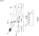
- the figure 9 illustrates certain quantities involved in the quantity of flux collected by each photo-detector in the architectures described above.
- Det denotes the detector.
- the total flux of photons F TOT/pix which reaches a photo-detector PD comprises a useful component of amplitude F AC/pix modulated at the frequency f R as defined above and corresponding to the interference between Lref/pix and Lo,r /pix, and a DC component F DC/pix .
- F early / pix F DC / pix + F AC / pix
- This modeling also applies to the integrated architecture by adapting the values of T1 0 and T2 0 to the integrated optical components. In this case the local oscillator beam does not pass through the optics Im.
- the lidar according to the invention integrates an intelligent optical module acting on the reference beam Lref (local oscillator), so that each signal received by a pixel of the imager and coming from the scene, can be amplified individually.
- Lref local oscillator
- an adjusted local oscillator on the one hand not to saturate each photoreceptor of the imager and on the other hand to have the best signal-to-noise ratio SNR.
- the second optical device D2 and the imaging optical system Im are further configured to superimpose, at the level of the photodetector component of a pixel and in a substantially identical direction of propagation, the pixel reference beam Lref/pix and the pixel image beam Lo,r/pix, forming a recombined pixel beam Lrec/pix.
- the photo-detector component of a pixel transforms the flux of photons into a proportional flux of electrons with a given quantum efficiency.
- the photo-detector component is configured to generate a Spix pixel detected signal from the pixel recombined beam, the detected pixel signal exhibiting an intensity called total pixel intensity I tot/pix (see figure 8 ).
- the detector is quantum efficient, and the detected electronic signal is proportional to the incident photon flux on the detector.
- the term signal (detected) and the term intensity (total) are used in an equivalent manner.
- the coherent lidar imaging system is further configured to determine, for each pixel, a frequency F(i,j) of a beat of the recombined beam.
- the coherent lidar imaging system 30 further comprising a processing unit UT configured to determine, for each pixel, a distance from points of the scene imaged on said pixels (and if applicable a speed) from the beat frequency associated with each pixel and from the modulated optical frequency of the laser radiation.
- the variant of the lidar 30 according to the invention with the propagation in free space of the reference beam is illustrated figure 10 .
- the reference beam also passes through the optics IM, which contributes to its routing towards the pixels of the detector.
- the separator DS of the lidar 30 of the separator has a first variable transmittance T1 which is identical for all the pixels and can be modulated. Unlike the splitter of the previous architectures, it is possible here to modify the relative ratio between the fraction of the emitted laser radiation F which constitutes the reference beam Lref and the fraction which illuminates the scene Lo.
- the transmittance T1 is electrically adjustable.
- the second optical device D2 of the lidar 30 comprises, in addition to the combiner DR, at least one intensity modulator IM adapted to modulate the intensity of each pixel reference beam Lref/pix by applying a modulated pixel transmittance.
- the modulator IM is a matrix component called SLM (for “spatial light modulator”) electrically controllable, positioned on the optical path of the reference beam Lref downstream of the splitter DS and upstream of the combiner device DR.
- the processing unit UT is configured to apply a first transmittance value T1 and, for each pixel, a pixel transmittance value xij, these values being determined via a feedback loop and according to an optimization criterion.
- the feedback loop is implemented in the processing unit but according to one embodiment at least a part is implemented on the detector.
- optimization parameters T1 and xij means the application of a condition to physical quantities.
- the optimization criterion comprises, for each pixel, obtaining a total pixel intensity I tot/pix lower than a threshold intensity Is and an improved signal-to-noise ratio SNR, which means increased, with respect to the value initial.
- the components allowing the implementation of the lidar 30 according to the invention are different depending on the type of architecture, but have similar functionality.
- the transmission factor, and therefore the reflection factor of the splitter is modified according to the quantity of backscattered light which returns from the scene.
- the individual amplification factor for each photoreceptor of the imager is also modified by introducing a pixelated intensity modulation on the path of the local oscillator.
- the intelligent optical module consists of the variable separator DS and the modulator IM. These two components are controlled by an electrical signal from the imager including all detected Spix signals. The signal received by each pixel now depends on variable T1 and on the parameter x ij between the value 0 (no transmission) and 1 (complete transmission).
- the global transmission/reflection of the splitter is adapted and locally the intensity of the local oscillator is adjusted for each pixel of the imager.
- T1 and xij are optimized in real time in order to have the best SNR ratio while having no saturated pixels.
- the total intensity detected for a pixel I tot/pix is proportional to the total photon flux F tot and breaks down into a modulated intensity I ACpix and a constant intensity I DCpix defined as follows: I AC / pix I I ⁇ 4 ⁇ ⁇ S I I ⁇ LO I I F you ⁇ cos 2 ⁇ f R you + ⁇ I DC / pix I I ⁇ ⁇ S I I ⁇ ⁇ LO I I 2 ⁇ F you
- the signal-to-noise ratio SNR of the detection used for the optimization is determined from the SNR pix of the pixels of the detector, and can be defined in different ways.
- this is an average signal-to-noise ratio defined as the average of the SNR pix of the pixels of the detector.
- SNR ⁇ SNR pix >
- the mean is arithmetic, or equal to the median.
- the SNR corresponds to the minimum of the SNR pix and the optimization consists in increasing this minimum.
- SNR min SNR pix
- a processing circuit for each pixel carries out a filtering of the DC component and an amplification of the modulated part of the detected signal.
- the optimization criterion includes two conditions: A first condition is that I tot/pix ⁇ Is for all the pixels of the detector Det. A second condition is the increase of the SNR compared to its value initial, under the constraint of the first condition.
- Different known algorithms can be used for implementing the optimization, such as Newton or genetics.
- the optimization criterion further comprises a third condition which is the obtaining, for each pixel, of a total intensity or of a modulated intensity that is also improved.
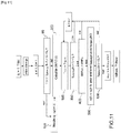
- the figure 11 presents an example of an algorithm integrating this last condition.
- xij we initialize xij to 1 and T1 to a value T1ini.
- the spatial intensity modulator IM assigns individual values xij for each pixel of the imager in order to have no saturation on the image (steps 90 and 100).
- the SNRs of all the pixels SNR pix are calculated then an SNR function (mean, median, min..) dependent on these SNR pix is determined (step 200).
- the value of T1 is then adjusted in order to increase this SNR function while taking care not to cause saturation: as long as it is possible to increase SNR while having no saturated pixel, we loop back (steps 300, 350 and 400 double loop over k and t).
- a step 500 local attempts are made to regain the intensity value (total or modulated) by re-increasing the xij, still remaining below saturation (step 600).
- a final value of T1 and a matrix of values xij corresponding to each pixel Pij with the best SNR are obtained.
- the general optimization philosophy is to first adjust xij to avoid any saturation, then adapt T1 to increase the SNR while remaining below saturation, then once the maximum SNR value is obtained, locally readjust xij to increase I tot/pix or I AC/pix when possible.
- the combiner DR also has an identical second modulable transmittance T2 for all the pixels, the processing unit being further configured to apply a second transmittance value via the servo loop BA and according to the optimization criterion.
- the transmittance T2 is electrically adjustable. The optimization is therefore carried out via three parameters T1, T2 and xij. In this case, the formulas for ⁇ s(i,j) and ⁇ LO(i,j) (3) and (4) should be modified by replacing T2 0 by variable T2.
- the relative % or ratio between the reference beam and the object beam which will recombine is in fact modulated. Having this additional parameter in the control loop makes it possible to obtain better optimization.
- the modification of T2 is carried out at the same time as that of T1.
- the optimization criterion also comprises obtaining a dispersion of the pixel signal-to-noise values reduced.
- ⁇ SNR the dispersion of the SNR pix .
- the figure 12 illustrates an example of an optimization algorithm integrating both the embodiment including the additional modulation of T2 and the embodiment taking into account the reduction in dispersion.
- a weight is attributed to each of the two conditions increase of the SNR and reduction of the ⁇ SNR.
- the value of the total intensity is given in number of electrons.
- the first step consists in modifying x (reducing its value) so as to lower the intensity of the Lref/pix beam for each pixel to bring them out of saturation.
- a 2nd adjustment of the value of x is carried out for each pixel (line 4 on the 2 tables).
- We even realize that we have returned to x 1 (max value) for pixel 2.
- T1 and T2 are to be optimized for an overall rendering of the SNR and of the signal (intensity) within the limits of non-saturation, over the entire detector.
- the values x ij they are mainly there for a local action on each pixel in order to avoid having saturated signals.
- the figure 15 illustrates the evolution of the signal for pixel 1 P1 as a function of T1 and T2, for different stages of the optimization.
- the upper part of the figure for a) to d) shows the 2D plot (or “mapping") of the signal I tot/pix as a function of T1 and T2 and for a fixed value of x(P1).
- the different signal values in number of electrons are indicated by levels of gray, the white color corresponding to the highest level, just before saturation.
- the saturation zone is indicated by hatching and a value of zero is assigned to the saturated signal.
- the figure 16 illustrates the evolution of the SNR for pixel 1 P1 as a function of T1 and T2 for the same optimization steps as on the figure 15 .
- the upper part of the figure 16 from a) to d) illustrates the 2D plot of the SNR for pixel 1 P1 as a function of T1 and T2 and for a value of x(P1).
- the saturation zone is indicated by hatching and a value of zero is assigned to the saturated signal.
- This increases the signal (see Figure 15d) ) and we also see that the SNR value has also increased a bit to 5 ( Figure 16d) ).
- the operating point of this pixel is located at the saturation limit (high signal value) with an SNR of approximately 5 optimized at best.
- the matrix component is an LC-SLM liquid crystal modulator in transmissive mode known to those skilled in the art.
- each pixel is controlled with circuitry often based on TFTs (Thin Film Transistors).
- TFTs Thin Film Transistors
- the reference beam is pixelated and the intensity passing through each pixel is controlled.
- this component must also be imaged optically on the plane of the detector so that each pixel of the SLM corresponds to a pixel P(i,j) of the detector.
- the separator DS is an electrically adjustable Fabry-Perot filter.
- the principle of a Fabry-Perot filter is to allow a light beam centered around a given wavelength ⁇ filter to pass with a certain width at mid-height ⁇ filter .
- modulable Fabry-Perot filters where a voltage comes to modulate the thickness of the cavity between the Bragg reflectors in order to shift the center of the range of transmitted wavelengths.
- a modular filter is used which makes it possible to position the laser working length ⁇ not at the center of the transmission curve of the filter but on one side of the curve of its spectral response.
- the figure 18 illustrates an embodiment of the lidar 30 according to the invention in free space in which the second optical device D2 further comprises an intermediate optical system SI adapted to form the intermediate image and arranged after the separator DS and the matrix component SLM and before the DR combiner.
- the intermediate optical system SI in combination with the imaging optical system Im is arranged to form an image of the matrix component SLM on the detection device Det.
- the figure 19 illustrates a lidar 35 according to the invention having an integrated architecture.
- the reference beam is here injected directly into each pixel at the detector, as shown figure 5 and 6 .
- the pixels of the detectors are distributed over N columns and M rows and at least part of the second optical device D2 conveying the reference beam to the photo-detectors PDij is integrated on the detector Det designed in integrated photonics.
- the device D2 comprises an optical guide called reference guide OGref configured to receive the reference beam and N optical guides OGC(i), called column guides, coupled to the reference guide (for example by evanescent coupling), and adapted to convey part of the reference beam in the N columns of the detector.
- Each column guide is coupled to M optical guides OGL(i,j) (for example by evanescent coupling), called line guides, respectively associated with the M pixels of the M lines of the detector of the column.
- the M line guides are configured to route part of the reference beam into each pixel of the column.
- the device D2 comprises an optical detection guide OGD(i,j) coupled to the photodetector component PD(i,j)), a diffraction grating, called pixel grating Rpix(i,j), configured to coupling the pixel image beam to the photo-detector component, typically a guided photodiode.
- the diffraction grating collects the light coming from the scene and couples it into a waveguide OGpix(i,j).
- the device D2 also comprises a coupler, called the pixel coupler Coup(i,j), configured to couple, in the detection guide OGD(i,j), the pixel image beam Lo,r/pix and the pixel reference beam Lref/ pix, thus forming the recombined beam Lrec/pix allowing heterodyne mixing of the two beams.
- a coupler called the pixel coupler Coup(i,j)
- the second device D2 also comprises an intensity modulator integrated per pixel IMI(i,j) placed in series with the line guide and placed before the pixel coupler Coup(i,j), and of which at least one of the branches is adjustable.
- the IMI(i,j) modulator is the equivalent of the pixelated SLM in free space optics.
- the intensity modulation of each Lref/pix beam is here performed locally, in each pixel.
- the DS separator is of the same type as that of lidar 30.
- the intensity modulator IMI(i,j) is an integrated Mach-Zender type interferometer illustrated figure 20 with one of its branches having a ZC coupling zone modulated thermally or by injection of carriers or by electro-optical modulation.
- the activation of the thermal or electrical modulation (done for example by a PIN diode) is controlled by the signal received by the photodiode.
- the integrated intensity modulator IMI(i,j) is a resonant ring AR as illustrated figure 21 , for example produced on a low index layer (example: BOX for "Buried Oxide” in English) deposited on a high index substrate SUB (example: silicon), like the other guided elements (in particular the waveguides) mentioned in the previous paragraphs.
- a low index layer example: BOX for "Buried Oxide” in English
- SUB example: silicon
- Part of the light which propagates in the waveguide couples in the AR ring (by evanescent coupling, the ring being located relatively close to the guide).
- the ring is resonant at the working wavelength i.e.
- the phase shift of the light after completing a full turn of the ring is a multiple of 2 ⁇ , so interference is constructive at the waveguide output straight between the light which has not been coupled in the ring and that which has been coupled in it, makes one or more turns, and has decoupled in the guide. So the output current is equal to the input current.
- the phase shift for one turn of the ring varies and the output intensity decreases, so we indeed have an intensity modulator.
- the modulation is performed by the pixel coupler Coup(i,j) which is a directional coupler that can be modulated, making it possible to vary a ratio R between the pixel reference beam and the pixel image beam in the Lrec beam.
- the processing unit UT is then configured to apply a ratio value via said feedback loop and according to the optimization criterion.
- a local modulation T2(i,j) is performed here and no longer a global modulation as in free space.
- this 2 ⁇ 2 directional coupler Coup(i,j) has on one of the branches a coupling zone ZC modulated thermally (lower part of the figure) or by injection of carriers (upper part) or by electro-optical modulation. This makes it possible to vary the coupling between the 2 arms and distribute the heterodyne signal between the 2 outputs of this coupler. One of the outputs is used to bring the signal to the photodiode PD, the other is not used, such as in free space where a path of the splitter blade is not used.
- the two output channels are coupled by a Y junction so that all the heterodyne signal can be guided towards the photoreceptor.
- the splitter DS, the second optical device D2 and the detector are made on the same substrate Sub.
- the splitter DS comprises an integrated optical circuit OC which is subdivided, via a modulating directional coupler JY, into, on the one hand, at least one waveguide comprising at least one diffraction grating, called an object grating OG, configured to decouple part of the laser beam from the plane of the integrated optical circuit so as to form the object beam L (via a projection device DP if necessary), and on the other hand a waveguide OGref devoid of grating guiding the reference beam up to to the detector.
- the detector comprises a matrix of microlenses ⁇ L(i,j) to focus the object beam in the pixels Pij of the detector.
- the modular directional coupler JY is an evanescent wave coupler.
- This type of coupler is illustrated figure 24 which presents a zoom of zone 3 of the figure 23 .
- the figure 25 illustrates two variants of the directional coupler.
- the figure 25 b) illustrates a thermally modulated coupling zone ZC' and the Figure 25 a) by injection of carriers (a PIN diode for example).
- the modulation can also be electro-optical.
- the modulation makes it possible to vary the ratio of the beam L going towards the diffraction grating (returning the light towards the scene) and the reference beam going towards the detector.
- the figure below shows the principle of an evanescent wave coupler. Note that in the examples of figure 22 and 25 the couplers Coup(i,j) and JY are the same component, used either to separate or to combine.
- the method according to the invention further comprises a step C′ consisting in applying a ratio value between the pixel reference beam and pixel image beam, the ratio value being determined by the servo loop.
Landscapes
- Engineering & Computer Science (AREA)
- Physics & Mathematics (AREA)
- Computer Networks & Wireless Communication (AREA)
- General Physics & Mathematics (AREA)
- Radar, Positioning & Navigation (AREA)
- Remote Sensing (AREA)
- Electromagnetism (AREA)
- Optical Radar Systems And Details Thereof (AREA)
Applications Claiming Priority (1)
| Application Number | Priority Date | Filing Date | Title |
|---|---|---|---|
| FR2007316A FR3112397B1 (fr) | 2020-07-10 | 2020-07-10 | Système lidar cohérent à rapport signal sur bruit amélioré |
Publications (2)
| Publication Number | Publication Date |
|---|---|
| EP3936887A1 true EP3936887A1 (de) | 2022-01-12 |
| EP3936887B1 EP3936887B1 (de) | 2023-05-10 |
Family
ID=73698930
Family Applications (1)
| Application Number | Title | Priority Date | Filing Date |
|---|---|---|---|
| EP21180453.9A Active EP3936887B1 (de) | 2020-07-10 | 2021-06-18 | Kohärentes lidar-system mit verbessertem signal-rausch-verhältnis |
Country Status (4)
| Country | Link |
|---|---|
| US (1) | US20220011432A1 (de) |
| EP (1) | EP3936887B1 (de) |
| CN (1) | CN113917485A (de) |
| FR (1) | FR3112397B1 (de) |
Families Citing this family (2)
| Publication number | Priority date | Publication date | Assignee | Title |
|---|---|---|---|---|
| DE102022202285A1 (de) | 2022-03-07 | 2023-09-07 | Volkswagen Aktiengesellschaft | Radarsensorvorrichtung, Radarsystem mit einer Radarsensorvorrichtung, Fahrzeug mit einem Radarsystem sowie Verfahren zum Betreiben einer Radarsensorvorrichtung |
| US12256155B2 (en) * | 2022-08-30 | 2025-03-18 | Lg Innotek Co., Ltd. | System and method for reducing stray light interference in optical systems |
Citations (4)
| Publication number | Priority date | Publication date | Assignee | Title |
|---|---|---|---|---|
| FR2000408A2 (de) | 1968-01-18 | 1969-09-05 | Int Standard Electric Corp | |
| FR2005186A1 (de) | 1968-03-30 | 1969-12-05 | Ajinomoto Kk | |
| JP2016105082A (ja) * | 2014-11-19 | 2016-06-09 | 株式会社豊田中央研究所 | レーザレーダ装置およびレーザレーダ装置の光受信方法 |
| US20190025431A1 (en) * | 2017-07-24 | 2019-01-24 | Telaris Inc. | Precisely controlled chirped diode laser and coherent lidar system |
Family Cites Families (9)
| Publication number | Priority date | Publication date | Assignee | Title |
|---|---|---|---|---|
| US6707054B2 (en) * | 2002-03-21 | 2004-03-16 | Eastman Kodak Company | Scannerless range imaging system having high dynamic range |
| US6860350B2 (en) * | 2002-12-20 | 2005-03-01 | Motorola, Inc. | CMOS camera with integral laser ranging and velocity measurement |
| JP2004205726A (ja) * | 2002-12-25 | 2004-07-22 | Yokogawa Electric Corp | ビームスプリッター |
| US8531753B1 (en) * | 2011-05-09 | 2013-09-10 | Los Alamos National Security, Llc | Adaptive optical filter |
| US9784958B2 (en) * | 2014-01-18 | 2017-10-10 | Daylight Solutions, Inc. | Low-noise spectroscopic imaging system using substantially coherent illumination |
| US10000000B2 (en) * | 2015-03-10 | 2018-06-19 | Raytheon Company | Coherent LADAR using intra-pixel quadrature detection |
| JP7140784B2 (ja) * | 2017-03-01 | 2022-09-21 | ポイントクラウド インコーポレイテッド | モジュラー三次元光学検知システム |
| JP6838705B2 (ja) * | 2017-03-30 | 2021-03-03 | 日本電気株式会社 | レーザレーダ装置及びそれに用いる強度画像取得方法 |
| DE102018212984A1 (de) * | 2018-08-03 | 2020-02-06 | Robert Bosch Gmbh | Vorrichtung zur Detektion eines Objekts |
-
2020
- 2020-07-10 FR FR2007316A patent/FR3112397B1/fr not_active Expired - Fee Related
-
2021
- 2021-06-18 EP EP21180453.9A patent/EP3936887B1/de active Active
- 2021-06-30 US US17/364,143 patent/US20220011432A1/en active Pending
- 2021-07-09 CN CN202110776099.4A patent/CN113917485A/zh active Pending
Patent Citations (4)
| Publication number | Priority date | Publication date | Assignee | Title |
|---|---|---|---|---|
| FR2000408A2 (de) | 1968-01-18 | 1969-09-05 | Int Standard Electric Corp | |
| FR2005186A1 (de) | 1968-03-30 | 1969-12-05 | Ajinomoto Kk | |
| JP2016105082A (ja) * | 2014-11-19 | 2016-06-09 | 株式会社豊田中央研究所 | レーザレーダ装置およびレーザレーダ装置の光受信方法 |
| US20190025431A1 (en) * | 2017-07-24 | 2019-01-24 | Telaris Inc. | Precisely controlled chirped diode laser and coherent lidar system |
Non-Patent Citations (2)
| Title |
|---|
| AFLATOUNI: "Nano photonic coherent imager", OPTICS EXPRESS, vol. 23, no. 4, 2015, pages 5117 |
| AUDE MARTIN ET AL: "Photonic Integrated Circuit-Based FMCW Coherent LiDAR", JOURNAL OF LIGHTWAVE TECHNOLOGY, vol. 36, no. 19, 1 October 2018 (2018-10-01), USA, pages 4640 - 4645, XP055764841, ISSN: 0733-8724, DOI: 10.1109/JLT.2018.2840223 * |
Also Published As
| Publication number | Publication date |
|---|---|
| US20220011432A1 (en) | 2022-01-13 |
| EP3936887B1 (de) | 2023-05-10 |
| FR3112397B1 (fr) | 2022-08-12 |
| CN113917485A (zh) | 2022-01-11 |
| FR3112397A1 (fr) | 2022-01-14 |
Similar Documents
| Publication | Publication Date | Title |
|---|---|---|
| EP4012453B1 (de) | Lidar-bildgebungssystem mit heterodyner detektion vom typ fmcw mit einer vorrichtung zur phasenkorrektur des referenzsignals | |
| EP4090993B1 (de) | Kohärentes lidar-abbildungssystem | |
| FR3049719B1 (fr) | Dispositifs et methodes de transport et de controle de faisceaux lumineux pour l'imagerie endo-microscopique sans lentille | |
| EP3936887B1 (de) | Kohärentes lidar-system mit verbessertem signal-rausch-verhältnis | |
| FR3059099A1 (fr) | Systeme de detection d'onde acoustique a fibre acoustique | |
| EP3913395B1 (de) | Verbesserter detektor mit umlenkelementen für kohärente bildgebung | |
| EP4362763B1 (de) | Bildgebungsverfahren, endoskop und computerprogrammprodukt | |
| EP3491330B1 (de) | Interferenzielle vollfeldbildgebungssysteme und verfahren | |
| EP4302148A1 (de) | System zur kompensation der verzerrung einer wellenfront eines einfallenden lichtstrahls | |
| FR2848664A1 (fr) | Detecteur de position, forme et reflectivite d'une surface | |
| EP3913393B1 (de) | Verbesserte detektionsvorrichtung und entsprechendes lidar-system | |
| WO2025012096A1 (fr) | Systeme lidar a detection directe | |
| EP2136239B1 (de) | Laservorrichtung, die Mittel zur Synchronisierung einer großen Anzahl von kohärenten Quellen umfasst | |
| FR3084158A1 (fr) | Methode et dispositif de caracterisation de filtres optiques | |
| FR3132947A1 (fr) | Systèmes et procédés d’analyse de la qualité de surface d’une lame à faces parallèles | |
| FR3143741A1 (fr) | Composant optique et analyseur de surface d’onde comprenant un tel composant optique | |
| FR3138946A1 (fr) | Dispositif optique, système et procédé d’interférométrie à dispersion | |
| EP4078217A1 (de) | Lidar-system mit zwei diffraktiven komponenten | |
| EP0591911A2 (de) | Interferometer bestehend aus einer integrierten Anordnung und einem reflektierenden Teil, die durch eine Messzone voneinander getrennt sind | |
| FR3064058A1 (fr) | Systeme optique et spectrometre miniature equipe d'un tel systeme ainsi que procede d'analyse d'objets a l'aide d'un tel systeme optique | |
| FR3075521A1 (fr) | Systeme de communication comprenant un dispositif de compensation a etoile artificielle |
Legal Events
| Date | Code | Title | Description |
|---|---|---|---|
| PUAI | Public reference made under article 153(3) epc to a published international application that has entered the european phase |
Free format text: ORIGINAL CODE: 0009012 |
|
| STAA | Information on the status of an ep patent application or granted ep patent |
Free format text: STATUS: REQUEST FOR EXAMINATION WAS MADE |
|
| 17P | Request for examination filed |
Effective date: 20210701 |
|
| AK | Designated contracting states |
Kind code of ref document: A1 Designated state(s): AL AT BE BG CH CY CZ DE DK EE ES FI FR GB GR HR HU IE IS IT LI LT LU LV MC MK MT NL NO PL PT RO RS SE SI SK SM TR |
|
| B565 | Issuance of search results under rule 164(2) epc |
Effective date: 20211213 |
|
| GRAP | Despatch of communication of intention to grant a patent |
Free format text: ORIGINAL CODE: EPIDOSNIGR1 |
|
| STAA | Information on the status of an ep patent application or granted ep patent |
Free format text: STATUS: GRANT OF PATENT IS INTENDED |
|
| INTG | Intention to grant announced |
Effective date: 20221201 |
|
| GRAS | Grant fee paid |
Free format text: ORIGINAL CODE: EPIDOSNIGR3 |
|
| GRAA | (expected) grant |
Free format text: ORIGINAL CODE: 0009210 |
|
| STAA | Information on the status of an ep patent application or granted ep patent |
Free format text: STATUS: THE PATENT HAS BEEN GRANTED |
|
| AK | Designated contracting states |
Kind code of ref document: B1 Designated state(s): AL AT BE BG CH CY CZ DE DK EE ES FI FR GB GR HR HU IE IS IT LI LT LU LV MC MK MT NL NO PL PT RO RS SE SI SK SM TR |
|
| REG | Reference to a national code |
Ref country code: GB Ref legal event code: FG4D Free format text: NOT ENGLISH |
|
| REG | Reference to a national code |
Ref country code: AT Ref legal event code: REF Ref document number: 1567214 Country of ref document: AT Kind code of ref document: T Effective date: 20230515 Ref country code: CH Ref legal event code: EP |
|
| REG | Reference to a national code |
Ref country code: DE Ref legal event code: R096 Ref document number: 602021002266 Country of ref document: DE |
|
| REG | Reference to a national code |
Ref country code: IE Ref legal event code: FG4D Free format text: LANGUAGE OF EP DOCUMENT: FRENCH |
|
| REG | Reference to a national code |
Ref country code: LT Ref legal event code: MG9D |
|
| REG | Reference to a national code |
Ref country code: NL Ref legal event code: MP Effective date: 20230510 |
|
| REG | Reference to a national code |
Ref country code: AT Ref legal event code: MK05 Ref document number: 1567214 Country of ref document: AT Kind code of ref document: T Effective date: 20230510 |
|
| PG25 | Lapsed in a contracting state [announced via postgrant information from national office to epo] |
Ref country code: SE Free format text: LAPSE BECAUSE OF FAILURE TO SUBMIT A TRANSLATION OF THE DESCRIPTION OR TO PAY THE FEE WITHIN THE PRESCRIBED TIME-LIMIT Effective date: 20230510 Ref country code: PT Free format text: LAPSE BECAUSE OF FAILURE TO SUBMIT A TRANSLATION OF THE DESCRIPTION OR TO PAY THE FEE WITHIN THE PRESCRIBED TIME-LIMIT Effective date: 20230911 Ref country code: NO Free format text: LAPSE BECAUSE OF FAILURE TO SUBMIT A TRANSLATION OF THE DESCRIPTION OR TO PAY THE FEE WITHIN THE PRESCRIBED TIME-LIMIT Effective date: 20230810 Ref country code: NL Free format text: LAPSE BECAUSE OF FAILURE TO SUBMIT A TRANSLATION OF THE DESCRIPTION OR TO PAY THE FEE WITHIN THE PRESCRIBED TIME-LIMIT Effective date: 20230510 Ref country code: ES Free format text: LAPSE BECAUSE OF FAILURE TO SUBMIT A TRANSLATION OF THE DESCRIPTION OR TO PAY THE FEE WITHIN THE PRESCRIBED TIME-LIMIT Effective date: 20230510 Ref country code: AT Free format text: LAPSE BECAUSE OF FAILURE TO SUBMIT A TRANSLATION OF THE DESCRIPTION OR TO PAY THE FEE WITHIN THE PRESCRIBED TIME-LIMIT Effective date: 20230510 |
|
| PG25 | Lapsed in a contracting state [announced via postgrant information from national office to epo] |
Ref country code: RS Free format text: LAPSE BECAUSE OF FAILURE TO SUBMIT A TRANSLATION OF THE DESCRIPTION OR TO PAY THE FEE WITHIN THE PRESCRIBED TIME-LIMIT Effective date: 20230510 Ref country code: PL Free format text: LAPSE BECAUSE OF FAILURE TO SUBMIT A TRANSLATION OF THE DESCRIPTION OR TO PAY THE FEE WITHIN THE PRESCRIBED TIME-LIMIT Effective date: 20230510 Ref country code: LV Free format text: LAPSE BECAUSE OF FAILURE TO SUBMIT A TRANSLATION OF THE DESCRIPTION OR TO PAY THE FEE WITHIN THE PRESCRIBED TIME-LIMIT Effective date: 20230510 Ref country code: LT Free format text: LAPSE BECAUSE OF FAILURE TO SUBMIT A TRANSLATION OF THE DESCRIPTION OR TO PAY THE FEE WITHIN THE PRESCRIBED TIME-LIMIT Effective date: 20230510 Ref country code: IS Free format text: LAPSE BECAUSE OF FAILURE TO SUBMIT A TRANSLATION OF THE DESCRIPTION OR TO PAY THE FEE WITHIN THE PRESCRIBED TIME-LIMIT Effective date: 20230910 Ref country code: HR Free format text: LAPSE BECAUSE OF FAILURE TO SUBMIT A TRANSLATION OF THE DESCRIPTION OR TO PAY THE FEE WITHIN THE PRESCRIBED TIME-LIMIT Effective date: 20230510 Ref country code: GR Free format text: LAPSE BECAUSE OF FAILURE TO SUBMIT A TRANSLATION OF THE DESCRIPTION OR TO PAY THE FEE WITHIN THE PRESCRIBED TIME-LIMIT Effective date: 20230811 |
|
| PG25 | Lapsed in a contracting state [announced via postgrant information from national office to epo] |
Ref country code: FI Free format text: LAPSE BECAUSE OF FAILURE TO SUBMIT A TRANSLATION OF THE DESCRIPTION OR TO PAY THE FEE WITHIN THE PRESCRIBED TIME-LIMIT Effective date: 20230510 |
|
| PG25 | Lapsed in a contracting state [announced via postgrant information from national office to epo] |
Ref country code: SK Free format text: LAPSE BECAUSE OF FAILURE TO SUBMIT A TRANSLATION OF THE DESCRIPTION OR TO PAY THE FEE WITHIN THE PRESCRIBED TIME-LIMIT Effective date: 20230510 |
|
| PG25 | Lapsed in a contracting state [announced via postgrant information from national office to epo] |
Ref country code: SM Free format text: LAPSE BECAUSE OF FAILURE TO SUBMIT A TRANSLATION OF THE DESCRIPTION OR TO PAY THE FEE WITHIN THE PRESCRIBED TIME-LIMIT Effective date: 20230510 Ref country code: SK Free format text: LAPSE BECAUSE OF FAILURE TO SUBMIT A TRANSLATION OF THE DESCRIPTION OR TO PAY THE FEE WITHIN THE PRESCRIBED TIME-LIMIT Effective date: 20230510 Ref country code: RO Free format text: LAPSE BECAUSE OF FAILURE TO SUBMIT A TRANSLATION OF THE DESCRIPTION OR TO PAY THE FEE WITHIN THE PRESCRIBED TIME-LIMIT Effective date: 20230510 Ref country code: EE Free format text: LAPSE BECAUSE OF FAILURE TO SUBMIT A TRANSLATION OF THE DESCRIPTION OR TO PAY THE FEE WITHIN THE PRESCRIBED TIME-LIMIT Effective date: 20230510 Ref country code: DK Free format text: LAPSE BECAUSE OF FAILURE TO SUBMIT A TRANSLATION OF THE DESCRIPTION OR TO PAY THE FEE WITHIN THE PRESCRIBED TIME-LIMIT Effective date: 20230510 Ref country code: CZ Free format text: LAPSE BECAUSE OF FAILURE TO SUBMIT A TRANSLATION OF THE DESCRIPTION OR TO PAY THE FEE WITHIN THE PRESCRIBED TIME-LIMIT Effective date: 20230510 |
|
| REG | Reference to a national code |
Ref country code: DE Ref legal event code: R097 Ref document number: 602021002266 Country of ref document: DE |
|
| REG | Reference to a national code |
Ref country code: BE Ref legal event code: MM Effective date: 20230630 |
|
| PG25 | Lapsed in a contracting state [announced via postgrant information from national office to epo] |
Ref country code: MC Free format text: LAPSE BECAUSE OF FAILURE TO SUBMIT A TRANSLATION OF THE DESCRIPTION OR TO PAY THE FEE WITHIN THE PRESCRIBED TIME-LIMIT Effective date: 20230510 |
|
| PG25 | Lapsed in a contracting state [announced via postgrant information from national office to epo] |
Ref country code: MC Free format text: LAPSE BECAUSE OF FAILURE TO SUBMIT A TRANSLATION OF THE DESCRIPTION OR TO PAY THE FEE WITHIN THE PRESCRIBED TIME-LIMIT Effective date: 20230510 |
|
| PG25 | Lapsed in a contracting state [announced via postgrant information from national office to epo] |
Ref country code: LU Free format text: LAPSE BECAUSE OF NON-PAYMENT OF DUE FEES Effective date: 20230618 |
|
| PLBE | No opposition filed within time limit |
Free format text: ORIGINAL CODE: 0009261 |
|
| STAA | Information on the status of an ep patent application or granted ep patent |
Free format text: STATUS: NO OPPOSITION FILED WITHIN TIME LIMIT |
|
| REG | Reference to a national code |
Ref country code: IE Ref legal event code: MM4A |
|
| PG25 | Lapsed in a contracting state [announced via postgrant information from national office to epo] |
Ref country code: LU Free format text: LAPSE BECAUSE OF NON-PAYMENT OF DUE FEES Effective date: 20230618 |
|
| PG25 | Lapsed in a contracting state [announced via postgrant information from national office to epo] |
Ref country code: IE Free format text: LAPSE BECAUSE OF NON-PAYMENT OF DUE FEES Effective date: 20230618 |
|
| 26N | No opposition filed |
Effective date: 20240213 |
|
| PG25 | Lapsed in a contracting state [announced via postgrant information from national office to epo] |
Ref country code: IE Free format text: LAPSE BECAUSE OF NON-PAYMENT OF DUE FEES Effective date: 20230618 |
|
| PG25 | Lapsed in a contracting state [announced via postgrant information from national office to epo] |
Ref country code: SI Free format text: LAPSE BECAUSE OF FAILURE TO SUBMIT A TRANSLATION OF THE DESCRIPTION OR TO PAY THE FEE WITHIN THE PRESCRIBED TIME-LIMIT Effective date: 20230510 |
|
| PG25 | Lapsed in a contracting state [announced via postgrant information from national office to epo] |
Ref country code: SI Free format text: LAPSE BECAUSE OF FAILURE TO SUBMIT A TRANSLATION OF THE DESCRIPTION OR TO PAY THE FEE WITHIN THE PRESCRIBED TIME-LIMIT Effective date: 20230510 Ref country code: IT Free format text: LAPSE BECAUSE OF FAILURE TO SUBMIT A TRANSLATION OF THE DESCRIPTION OR TO PAY THE FEE WITHIN THE PRESCRIBED TIME-LIMIT Effective date: 20230510 Ref country code: BE Free format text: LAPSE BECAUSE OF NON-PAYMENT OF DUE FEES Effective date: 20230630 |
|
| PG25 | Lapsed in a contracting state [announced via postgrant information from national office to epo] |
Ref country code: BG Free format text: LAPSE BECAUSE OF FAILURE TO SUBMIT A TRANSLATION OF THE DESCRIPTION OR TO PAY THE FEE WITHIN THE PRESCRIBED TIME-LIMIT Effective date: 20230510 |
|
| PG25 | Lapsed in a contracting state [announced via postgrant information from national office to epo] |
Ref country code: BG Free format text: LAPSE BECAUSE OF FAILURE TO SUBMIT A TRANSLATION OF THE DESCRIPTION OR TO PAY THE FEE WITHIN THE PRESCRIBED TIME-LIMIT Effective date: 20230510 |
|
| REG | Reference to a national code |
Ref country code: CH Ref legal event code: PL |
|
| PG25 | Lapsed in a contracting state [announced via postgrant information from national office to epo] |
Ref country code: CH Free format text: LAPSE BECAUSE OF NON-PAYMENT OF DUE FEES Effective date: 20240630 |
|
| PGFP | Annual fee paid to national office [announced via postgrant information from national office to epo] |
Ref country code: DE Payment date: 20250618 Year of fee payment: 5 |
|
| PGFP | Annual fee paid to national office [announced via postgrant information from national office to epo] |
Ref country code: GB Payment date: 20250625 Year of fee payment: 5 |
|
| PGFP | Annual fee paid to national office [announced via postgrant information from national office to epo] |
Ref country code: FR Payment date: 20250623 Year of fee payment: 5 |
|
| PG25 | Lapsed in a contracting state [announced via postgrant information from national office to epo] |
Ref country code: CY Free format text: LAPSE BECAUSE OF FAILURE TO SUBMIT A TRANSLATION OF THE DESCRIPTION OR TO PAY THE FEE WITHIN THE PRESCRIBED TIME-LIMIT; INVALID AB INITIO Effective date: 20210618 |
|
| PG25 | Lapsed in a contracting state [announced via postgrant information from national office to epo] |
Ref country code: HU Free format text: LAPSE BECAUSE OF FAILURE TO SUBMIT A TRANSLATION OF THE DESCRIPTION OR TO PAY THE FEE WITHIN THE PRESCRIBED TIME-LIMIT; INVALID AB INITIO Effective date: 20210618 |
|
| PG25 | Lapsed in a contracting state [announced via postgrant information from national office to epo] |
Ref country code: TR Free format text: LAPSE BECAUSE OF FAILURE TO SUBMIT A TRANSLATION OF THE DESCRIPTION OR TO PAY THE FEE WITHIN THE PRESCRIBED TIME-LIMIT Effective date: 20230510 |