EP3940763A1 - Procédé de fabrication d'une structure semiconductrice - Google Patents
Procédé de fabrication d'une structure semiconductrice Download PDFInfo
- Publication number
- EP3940763A1 EP3940763A1 EP20185786.9A EP20185786A EP3940763A1 EP 3940763 A1 EP3940763 A1 EP 3940763A1 EP 20185786 A EP20185786 A EP 20185786A EP 3940763 A1 EP3940763 A1 EP 3940763A1
- Authority
- EP
- European Patent Office
- Prior art keywords
- layer
- recess
- mask layer
- semiconductor device
- monocrystalline silicon
- Prior art date
- Legal status (The legal status is an assumption and is not a legal conclusion. Google has not performed a legal analysis and makes no representation as to the accuracy of the status listed.)
- Pending
Links
Images


Classifications
-
- H—ELECTRICITY
- H10—SEMICONDUCTOR DEVICES; ELECTRIC SOLID-STATE DEVICES NOT OTHERWISE PROVIDED FOR
- H10D—INORGANIC ELECTRIC SEMICONDUCTOR DEVICES
- H10D84/00—Integrated devices formed in or on semiconductor substrates that comprise only semiconducting layers, e.g. on Si wafers or on GaAs-on-Si wafers
- H10D84/01—Manufacture or treatment
- H10D84/02—Manufacture or treatment characterised by using material-based technologies
- H10D84/08—Manufacture or treatment characterised by using material-based technologies using combinations of technologies, e.g. using both Si and SiC technologies or using both Si and Group III-V technologies
-
- H—ELECTRICITY
- H10—SEMICONDUCTOR DEVICES; ELECTRIC SOLID-STATE DEVICES NOT OTHERWISE PROVIDED FOR
- H10P—GENERIC PROCESSES OR APPARATUS FOR THE MANUFACTURE OR TREATMENT OF DEVICES COVERED BY CLASS H10
- H10P14/00—Formation of materials, e.g. in the shape of layers or pillars
- H10P14/20—Formation of materials, e.g. in the shape of layers or pillars of semiconductor materials
- H10P14/27—Formation of materials, e.g. in the shape of layers or pillars of semiconductor materials using selective deposition, e.g. simultaneous growth of monocrystalline and non-monocrystalline semiconductor materials
- H10P14/271—Formation of materials, e.g. in the shape of layers or pillars of semiconductor materials using selective deposition, e.g. simultaneous growth of monocrystalline and non-monocrystalline semiconductor materials characterised by the preparation of substrate for selective deposition
- H10P14/272—Formation of materials, e.g. in the shape of layers or pillars of semiconductor materials using selective deposition, e.g. simultaneous growth of monocrystalline and non-monocrystalline semiconductor materials characterised by the preparation of substrate for selective deposition using mask materials other than SiO2 or SiN
-
- H—ELECTRICITY
- H10—SEMICONDUCTOR DEVICES; ELECTRIC SOLID-STATE DEVICES NOT OTHERWISE PROVIDED FOR
- H10P—GENERIC PROCESSES OR APPARATUS FOR THE MANUFACTURE OR TREATMENT OF DEVICES COVERED BY CLASS H10
- H10P14/00—Formation of materials, e.g. in the shape of layers or pillars
- H10P14/20—Formation of materials, e.g. in the shape of layers or pillars of semiconductor materials
- H10P14/29—Formation of materials, e.g. in the shape of layers or pillars of semiconductor materials characterised by the substrates
- H10P14/2901—Materials
- H10P14/2902—Materials being Group IVA materials
- H10P14/2905—Silicon, silicon germanium or germanium
-
- H—ELECTRICITY
- H10—SEMICONDUCTOR DEVICES; ELECTRIC SOLID-STATE DEVICES NOT OTHERWISE PROVIDED FOR
- H10P—GENERIC PROCESSES OR APPARATUS FOR THE MANUFACTURE OR TREATMENT OF DEVICES COVERED BY CLASS H10
- H10P14/00—Formation of materials, e.g. in the shape of layers or pillars
- H10P14/20—Formation of materials, e.g. in the shape of layers or pillars of semiconductor materials
- H10P14/29—Formation of materials, e.g. in the shape of layers or pillars of semiconductor materials characterised by the substrates
- H10P14/2924—Structures
- H10P14/2925—Surface structures
-
- H—ELECTRICITY
- H10—SEMICONDUCTOR DEVICES; ELECTRIC SOLID-STATE DEVICES NOT OTHERWISE PROVIDED FOR
- H10P—GENERIC PROCESSES OR APPARATUS FOR THE MANUFACTURE OR TREATMENT OF DEVICES COVERED BY CLASS H10
- H10P14/00—Formation of materials, e.g. in the shape of layers or pillars
- H10P14/20—Formation of materials, e.g. in the shape of layers or pillars of semiconductor materials
- H10P14/29—Formation of materials, e.g. in the shape of layers or pillars of semiconductor materials characterised by the substrates
- H10P14/2926—Crystal orientations
-
- H—ELECTRICITY
- H10—SEMICONDUCTOR DEVICES; ELECTRIC SOLID-STATE DEVICES NOT OTHERWISE PROVIDED FOR
- H10P—GENERIC PROCESSES OR APPARATUS FOR THE MANUFACTURE OR TREATMENT OF DEVICES COVERED BY CLASS H10
- H10P14/00—Formation of materials, e.g. in the shape of layers or pillars
- H10P14/20—Formation of materials, e.g. in the shape of layers or pillars of semiconductor materials
- H10P14/32—Formation of materials, e.g. in the shape of layers or pillars of semiconductor materials characterised by intermediate layers between substrates and deposited layers
- H10P14/3202—Materials thereof
- H10P14/3238—Materials thereof being insulating materials
-
- H—ELECTRICITY
- H10—SEMICONDUCTOR DEVICES; ELECTRIC SOLID-STATE DEVICES NOT OTHERWISE PROVIDED FOR
- H10P—GENERIC PROCESSES OR APPARATUS FOR THE MANUFACTURE OR TREATMENT OF DEVICES COVERED BY CLASS H10
- H10P14/00—Formation of materials, e.g. in the shape of layers or pillars
- H10P14/20—Formation of materials, e.g. in the shape of layers or pillars of semiconductor materials
- H10P14/34—Deposited materials, e.g. layers
- H10P14/3402—Deposited materials, e.g. layers characterised by the chemical composition
- H10P14/3404—Deposited materials, e.g. layers characterised by the chemical composition being Group IVA materials
- H10P14/3411—Silicon, silicon germanium or germanium
-
- H—ELECTRICITY
- H10—SEMICONDUCTOR DEVICES; ELECTRIC SOLID-STATE DEVICES NOT OTHERWISE PROVIDED FOR
- H10P—GENERIC PROCESSES OR APPARATUS FOR THE MANUFACTURE OR TREATMENT OF DEVICES COVERED BY CLASS H10
- H10P14/00—Formation of materials, e.g. in the shape of layers or pillars
- H10P14/20—Formation of materials, e.g. in the shape of layers or pillars of semiconductor materials
- H10P14/34—Deposited materials, e.g. layers
- H10P14/3402—Deposited materials, e.g. layers characterised by the chemical composition
- H10P14/3414—Deposited materials, e.g. layers characterised by the chemical composition being group IIIA-VIA materials
- H10P14/3416—Nitrides
-
- H—ELECTRICITY
- H10—SEMICONDUCTOR DEVICES; ELECTRIC SOLID-STATE DEVICES NOT OTHERWISE PROVIDED FOR
- H10P—GENERIC PROCESSES OR APPARATUS FOR THE MANUFACTURE OR TREATMENT OF DEVICES COVERED BY CLASS H10
- H10P50/00—Etching of wafers, substrates or parts of devices
- H10P50/69—Etching of wafers, substrates or parts of devices using masks for semiconductor materials
- H10P50/691—Etching of wafers, substrates or parts of devices using masks for semiconductor materials for Group V materials or Group III-V materials
- H10P50/692—Etching of wafers, substrates or parts of devices using masks for semiconductor materials for Group V materials or Group III-V materials characterised by their composition, e.g. multilayer masks or materials
Definitions
- the present invention relates to a method of manufacturing a semiconductor structure and to an intermediate semiconductor structure manufactured therefrom.
- Combining III-N based semiconductor devices with Si based semiconductor devices on a common base Si substrate can open routes for high power and high-performance electronic device applications and new possibilities for RF integrated circuits.
- III-N based semiconductor devices are typically manufactured on sapphire substrates, on SiC substrates or on Si (111) substrates.
- III-N based semiconductor devices it is difficult to selectively grow III-N based semiconductor devices on Si substrates to allow true monolithic integration with Si based semiconductor devices on that common Si substrate. Furthermore, monolithic co-integration of III-N based semiconductor devices with Si-based semiconductor devices on a common base Si substrate should be made feasible in such a way that the manufacturing should neither jeopardize fab throughput nor process yield.
- the present invention relates to a method for manufacturing a semiconductor structure, the semiconductor structure comprising an III-N semiconductor device in a first region and a silicon semiconductor device in a second region, the method comprising:
- the present invention relates to an intermediate semiconductor structure for integrating a III-N semiconductor device with a silicon semiconductor device comprising:
- thermal budget for manufacturing the III-N semiconductor device does not jeopardize the device reliability and device manufacturability of the silicon semiconductor device.
- an element described herein of an apparatus embodiment is an example of a means for carrying out the function performed by the element for the purpose of carrying out the invention.
- leakage blocking capability refers to enabling the control of the leakage current from the top to the substrate, whereby the device is usually biased at 50-100V or higher (for high voltage power) at the top of the stack.
- RF communication application refer to applications using RF power amplifier, RF switches.
- RF power application refer to application using RF heating.
- power electronics application refers to application dealing with power conversion.
- interrupted mask layer refers to the mask layer having a discontinuity.
- topography refers to the configuration or arrangement of physical features on a surface such as for instance the surface having concave or convex features or being flat in some parts.
- monolithic integration refers to using different device components to form integrated circuits that are built on a single semiconductor base material or single chip.
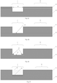
- FIG.1 showing a flowchart representing a method (1000) according to a first aspect of the present invention
- Fig. 2 and Fig. 3 showing schematic representation of the process steps, in sequential order, as used in embodiments of the first aspect of the present invention.
- the method (1000) comprises providing (100) a monocrystalline silicon base layer (10).
- This layer comprises a first region (I) for manufacturing a III-N semiconductor device and a second region (II) for manufacturing a silicon semiconductor device ( Fig. 2a and Fig. 3a ).
- the monocrystalline silicon base layer (10) may be a Si(111) layer or a Si(100) layer. It is advantageous to use the Si(100) layer since it allows for an easy fabrication of the Si semiconductor device. However, either Si(111) or Si(100) layer can be used to accommodate the monolithic integration of the III-N semiconductor device with the Si semiconductor device, thanks to the method of the present invention.
- the monocrystalline silicon base layer (10) may be comprised in a substrate and provided on an insulator layer.
- This monocrystalline silicon base layer is then referred to as a silicon on insulator (SOI) layer.
- the insulator layer may be a layer of an oxide, preferably a layer of silicon oxide.
- This substrate may further comprise a silicon bulk layer underneath the insulator layer.
- the silicon bulk layer may have (111) orientation.
- the monocrystalline silicon base layer comprised in this substrate may be (100) oriented.
- the method (1000) then comprises providing (200) a mask layer (30) on the monocrystalline silicon base layer (10) ( Fig. 1 ).
- This mask layer (10) comprises a 2-dimensional (2D) material and it is interrupted (31).
- the mask layer (30) comprising the 2D material can be provided on the monocrystalline silicon base layer (10) by, for instance, a chemical vapor deposition (CVD) process that is performed at temperatures higher than 700 °C, such as for instance, at a temperature between 900 °C to 1000 °C.
- CVD chemical vapor deposition
- a hydrocarbon precursor such as for instance, methane can be used.
- a metal layer needs to be provided on the monocrystalline silicon base layer (10) prior to the CVD process to act as a catalyst to facilitate the CVD growth of the layer of the 2D material.
- the layer of the 2D material (30) can be grown on a separate substrate. This layer can then be transferred on to the monocrystalline silicon base layer (10) by a transfer technique. In order to avoid delamination of the layer of the 2D material (30) from the monocrystalline silicon base layer, an adhesion layer needs to be provided on the monocrystalline silicon base layer (10) prior to the transfer process.
- a mask layer comprising a 2D material, which is interrupted (31) provides another advantage such that the manufacturing of the III-N semiconductor device can be done prior to the manufacturing of the silicon semiconductor device.
- the provision of this mask layer (30) is easier on the monocrystalline silicon base layer (10) either by performing the CVD process such as mentioned above or by transfer from another substrate and even a single layer of a 2D material would be sufficient to act as the mask layer (30).
- this provision is done by growing the mask layer comprising the 2D material (30) by performing a CVD process, the monocrystalline silicon base layer is to be subjected to temperatures higher than 700 °C, which can be detrimental for a prior existing silicon semiconductor device due to such high thermal budget.
- This mask layer is interrupted (31) such as, for instance, shown in Fig. 2d and in Fig. 3c , in the first region (I) by a recess (20) in the monocrystalline silicon base layer (10). Interrupted mask layer (31), as such, thus implies that the continuity of the mask layer is broken.
- This recess has sidewalls (21) and a bottom (22).
- This recess (20) is to be used for the manufacturing of a III-N semiconductor device.
- the depth of the recess (20) may, thus, be tailored according to the technological requirements for the manufacturing of the III-N semiconductor device.
- the width of the recess may range from a hundred nanometer to a few tens of micrometers or up to 100 nm or higher.
- the interrupted mask layer (31) comprises a 2D material since the unique structure of 2D material results in a highly inert, trap-free basal surface.
- This enables, in turn, the formation of the layer of gamma Al 2 O 3 (50) selectively at the bottom of the recess (20) since the inert surface of the mask layer comprising the 2D material will avoid the nucleation and hence further deposition of the layer of gamma Al 2 O 3 (50).
- formation of the III-N semiconductor device stack (40) will also be selectively done on the layer of gamma Al 2 O 3 (50) in the recess (20), again thanks to the inert surface of the mask layer comprising the 2D material.
- a single layer of 2D material may be sufficient to act as the mask layer.
- 2D materials two dimensions are outside the nanoscale and one dimension is only a single, such as in graphene, or more than one, such as in hexagonal BN or transition metal dichalcogenides, atomic layers thick.
- the thickness of 2D materials is different for different materials due to the fact that lattice constants are different.
- lattice constants are different.
- the W atom is covalently bonded to two S atoms within each individual layer, whereas van der Waals interactions govern in between two individual layers.
- Layer thickness of a single layer of WS2 is 0.615 nm. Single layers are obtained by exfoliation or by vapor phase transfer, chemical vapor deposition or molecular beam deposition.
- the mask layer may be a multi-layer stack of 2D materials.
- a patterning process typically, comprises performing a lithography process comprising photoresist coating, exposure and development of the photoresist. It further comprises performing an etch process to remove the material that does not follow the pattern identified by the exposed and developed photoresist in the lithography process.
- the aforementioned damage in the topmost layer can be caused by the etch process, which is comprised in the patterning process, in order to form the interrupted mask layer (31).
- Such damages can also be caused, in embodiments, by the etch process, which is comprised in the patterning process used to interrupt the mask layer ( Fig. 2d ).
- the mask layer is interrupted (31) such that it is not present at the bottom (22) of the recess (20).
- the layers of 2D material underneath the topmost layer are still highly inert and have trap-free basal surface.
- Such a damage in the topmost layer can be caused, in other embodiments, by the etch process, which is comprised in the patterning process, in order to interrupt the mask layer, which leads to the formation of the recess (20) in the monocrystalline silicon base layer ( Fig. 3c ).
- Si etching may be done as known to person skilled in the art, such as for instance by dry etching and using SF 6 /O 2 chemistry or by Cl 2 /HBr chemistry.
- the mask layer is interrupted (31) such that it is not present on the sidewalls (21) and at the bottom (22) of the recess (20).
- the multi-stack layer may consist of layers of the same 2D material. In alternative embodiments, the multi-stack layer may have alternating layers of two different 2D materials.
- the mask layer may comprise a topmost layer comprising a dielectric material.
- This dielectric material-comprising topmost layer may be provided on a single layer of a 2D material or on a multi-layer stack of 2D materials.
- this dielectric material comprising topmost layer since during a patterning step, which comprise a lithography process and an etch process, any possible damage that may be caused by the etch process can be absorbed by this topmost layer. This protects the layer or layers of 2D materials underneath this topmost layer comprising the dielectric material.
- this dielectric material may be a high-k dielectric material deposited by an atomic layer deposition (ALD) process. Provision of this high-k dielectric material is advantageous because a mild deposition can be enabled through the ALD in the temperature range of room temperature up to 300 °C so that the 2D material is not damaged. In this ALD process, short purge times and such low temperatures are beneficial since nucleation on the inert basal planes of 2D materials can be enabled at low temperatures due to contributions from physisorption.
- ALD atomic layer deposition
- the interruption of the mask layer (31) can be due to the fact that the mask layer (30) is not present at the bottom (22) of the recess (20) such as, for instance, shown in Fig. 2d .
- the recess (20) may be formed before providing the mask layer (30) on the monocrystalline silicon base layer (10) such as shown, for instance, in Fig. 2b .
- a patterning process may be performed comprising a lithography process followed by an etch process in order to make the recess (20) in the first region (I) in the monocrystalline silicon base layer (10).
- Si etching may be done as known to person skilled in the art, such as for instance by dry etching and using SF 6 /O 2 chemistry or by Cl 2 /HBr chemistry.
- the mask layer (30) may be deposited conformally on the monocrystalline silicon base layer (10).
- This conformal mask layer then covers the top surface of the monocrystalline silicon base layer (10) and the sidewalls (21) and bottom (22) of the recess (20) ( Fig. 2c ).
- This conformal deposition of the layer of the 2D material may be done by a chemical vapor deposition (CVD) process that can be performed at temperatures higher than 700 °C, such as for instance, at a temperature between 900 °C to 1000 °C, since conformal provision of the layer of 2D material by a transfer process in these embodiments could be cumbersome.
- a hydrocarbon precursor such as for instance, methane can be used to form the layer of 2D material.
- a metal layer needs to be provided on the monocrystalline silicon base layer (10) prior to the CVD process to act as a catalyst to facilitate the CVD growth of the layer of the 2D material.
- This metal layer can, such as for instance, be copper for growing graphene monolayer and nickel for growing multilayers of 2D materials.
- Another patterning process comprising a lithography process followed by an etch process may be performed to remove the mask layer (30) from the bottom (22) of the recess (20), thus interrupting the mask layer (30) and thereby exposing the monocrystalline silicon base layer at the bottom (22) of the recess (20), such as shown, for instance, in Fig. 2d .
- the mask layer is a multi-layer stack of 2D materials
- a topmost layer of the multi-layer stack is preferably to be removed after performing the etch process. This topmost layer is likely to be damaged due to the etch process and its removal provides the advantage of exposing a pristine layer of 2D material having highly inert surface and having trap-free basal surface.
- a lithography mask having an opening with a width that is smaller than the width (w) of the recess (30) after provision of the conformal layer of the 2D material ( Fig. 2c ) can be used.
- This is advantageous since it avoids removal of the layer of the 2D material (30), by the etch process, from regions falling outside the recess (20). This can be caused by alignment problems that can occur during the lithography process comprised in the patterning process used for interrupting the mask layer (30). This can lead to non-selectivity problems during the up-coming deposition processes.
- Patterning with such a lithography mask leads to the formation of two necks (23) of the layer of the 2D material (30) at the bottom (22) of the recess (20) such as shown, for instance, in Fig. 2e .
- the provision of the layer of gamma Al 2 O 3 (50) can proceed starting at the bottom of the recess (20) on the exposed monocrystalline silicon base layer (10) and proceed by selective lateral overgrowth.
- the width of the recess (20) is on the order of hundred nanometer or a few hundreds of nanometers
- the width of the opening of the lithography mask may be 10 to 95 percent of the width of the recess (20).
- the opening of the lithography mask may be in the range of 10 nm to 95 nm.
- the mask opening of 10 nm deposition of the layer of gamma Al 2 O 3 (50) can proceed starting at the bottom of the recess (20), while with a mask opening of 95 nm, alignment problems can also be handled while facilitating the deposition of the layer of gamma Al 2 O 3 (50) at the bottom of the recess (20).
- the width of the recess (20) is on the order of few tens of micrometers or up to 100 nm or higher, the width of the opening of the lithography mask may be 5 to 99 percent of the width of the recess (20).
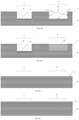
- the interruption of the mask layer (30) can also be due to the fact that it is not present on the sidewalls (21) and at the bottom (22) of the recess (20) such as, for instance, shown in Fig. 3c .
- the mask layer (30) may be provided on the monocrystalline silicon base layer (10) ( Fig. 3b ) before performing the patterning process to form the recess (20).
- the mask layer (30) may be provided on the monocrystalline silicon base layer (10) either by the aforementioned CVD process or by the aforementioned transfer process.
- Performing the patterning process comprising a lithography process followed by an etch process, then leads to the formation of the recess (20) ( Fig. 3c ).
- This etch process is typically a dry etch process and is executed as known to the person skilled in the art, such as for instance by dry etching and using SF 6 /O 2 chemistry or by Cl 2 /HBr chemistry.
- the bottom (22) of the recess (20) lies parallel to the top surface (11) of the monocrystalline silicon base layer (10).
- one or more layers from a top of the mask layer (30) may be removed. This removal is done so as to leave at least one layer in the mask layer. This removal may be done by performing an atomic layer etching in order to provide removal with atomic layer precision. Removal of the one or more layers from a top of the mask layer (30) is advantageous since this eliminates the aforementioned damaged topmost layer.
- This damaged topmost layer in some embodiments, may correspond to the topmost layer comprising the dielectric material, which itself is comprised in the mask layer. In embodiments, where this topmost layer is provided on a single layer of 2D material, its removal leads to the exposure of the highly inert, trap-free basal surface of the 2D material that is protected.
- this topmost layer comprising the dielectric material is provided on a multi-layer stack of 2D materials
- its removal also leads to the exposure of the highly inert, trap-free basal surface of the 2D material that is protected.
- use of a selective etch chemistry is advantageous in order to protect the 2D material that is to be exposed after its removal.
- a further layer or layers of the 2D material may be removed from the multi-layer stack of 2D materials, such as for instance by performing an atomic layer etching process.
- removal of the damaged topmost layer of the multi-layer stack then exposes an undamaged top surface of the remaining part of the multi-layer stack, thereby maintaining the possibility to perform the selective depositions needed in the recess (20) such as shown, for instance, in Fig. 2f or Fig. 3d .
- the interruption of the mask layer exposes the monocrystalline silicon base layer on the sidewalls (21) and at the bottom (22) of the recess (20).
- interruption is obtained due to the forming of the recess (20) in the monocrystalline silicon base layer (10).
- a layer of a passivating material may be provided on the sidewalls (21) of the recess (20) before forming, selectively, the layer of gamma-Al 2 O 3 (50) ( Fig. 3e ).
- the layer of the passivating material eliminates the interaction of the precursors used during the formation of the layer of gamma-Al 2 O 3 and/or the formation of the III-N semiconductor device stack with the monocrystalline silicon base layer (10).
- the formation of these layers can be done by a molecular beam epitaxy (MBE) process or by metal organic chemical vapor deposition (MOCVD) process. If the interaction of the precursors with the monocrystalline silicon base layer is not avoided, it can lead to the formation of defects in the monocrystalline silicon base layer (10), which then degrades the electrical and structural reliability of the III-N semiconductor device.
- the then-obtained topmost layer which is obtained after removal of the damaged topmost layer of the multi-layer stack, can further be damaged as a result of the patterning process used to remove the layer of a passivating material from the bottom (22) of the recess (20) ( Fig. 3e ), again mainly due to the etch process that is comprised in the patterning process. Removal of this damaged topmost layer is advantageous prior to carrying out the selective deposition of the layer of gamma-Al 2 O 3 (50) and for the deposition of the III-N semiconductor device stack ( Fig. 2f or Fig. 3f ) since removal would expose the highly inert, trap-free basal surface of the layer of the 2D material underneath.
- the formation of the layer of gamma-Al 2 O 3 (50) can be done by MOCVD using TMAI and N 2 O as precursors at around 1000 °C.
- the provision of the layer of the passivating material on the sidewalls comprises providing a conformal layer of the passivating material (70) on the sidewalls (21) and at the bottom (22) of the recess (20).
- this provision may be done by performing an ALD process.
- the ALD process leads to the provision of the layer of the passivating material (70) on the sidewalls (21) and bottom (22) of the recess (20) as well as on the interrupted mask layer (31).
- an extra patterning process comprising a lithography process and an etch process can be performed to remove the layer of the passivating material from the top of the interrupted mask layer (31).
- the layer of the passivating material (70) can be removed from the horizontal surfaces in one step, such as for instance removing it from the top of the interrupted mask layer (31) and from the bottom (22) of the recess (20).
- the layer of the passivating material (70) can be provided only on the sidewalls (21) and bottom (22) of the recess (20), such as for instance when aminosilanes are used.
- using a passivating material that helps to passivate defects on the interrupted mask layer (31) would be advantageous when deposited by ALD conformally on the interrupted mask layer (31) and inside the recess (20).
- the layer of the passivating material can be kept on the interrupted mask layer (31) due to this advantageous effect. Removing the layer of the passivating material (70) from the bottom (22) of the recess (20) then exposes the monocrystalline silicon base layer (10) ( Fig. 3e ). This removal can be done by another patterning step comprising a lithography process and an etch process.
- a lithography mask having an opening with a width that is smaller than the width (w) of the recess (30) after provision of the conformal layer of the passivating material (70) can be used, such as for instance going from Fig. 3d to Fig. 3e .
- This is advantageous since it avoids damage to or removal of the layer of the passivating material (70) on the sidewalls (21) that may originate from alignment issues during the lithography process. This can lead to interaction of the precursors used during the deposition of the layer of gamma Al 2 O 3 and/or the III-N semiconductor device stack in the recess (20).
- Such a lithography process done by using a lithography mask having an opening with a width that is smaller than the width (w) of the recess (30) leads to the formation of two necks of the layer of the passivating material at the bottom (22) of the recess (20) (not shown in the figures).
- the provision of the layer of gamma Al 2 O 3 (50) can proceed starting at the bottom of the recess (20) on the exposed monocrystalline silicon base layer (10) and proceed by selective lateral overgrowth.
- the width of the opening of the lithography mask may be 10 to 95 percent of the width of the recess (20).
- the opening of the lithography mask may be in the range of 10 nm to 95 nm.
- the width of the recess (20) is on the order of few tens of micrometers or up to 100 nm or higher, the width of the opening of the lithography mask may be 5 to 99 percent of the width of the recess (20).
- a layer of a dielectric material acting as a sacrificial material may be provided on the interrupted mask layer (31) in case the mask layer (30), such as, for instance, shown in ( Fig. 3b ) comprised a topmost layer comprising a dielectric material provided on a single layer of a 2D material. This is because, following the interruption of the mask layer (30) to create the interrupted mask layer (31) ( Fig.
- this topmost layer comprising the dielectric material, which absorbed any possible damage due to the etch process is removed, in order to expose the pristine surface of the 2D material to facilitate the selective deposition of the layer of the passivating material on the sidewalls (22) and at the bottom (21) of the recess (20). Therefore, before moving on to the removal of the layer of the passivating material (70) from the bottom (22) of the recess (20) ( Fig. 3e ), provision of such a layer of a dielectric material acting as a sacrificial layer will be advantageous to protect the interrupted mask layer (31) during the etching process comprised in the patterning process.
- a layer of a high-k dielectric material may be provided by ALD, selectively on the interrupted mask layer (31) at a temperature in the temperature range of room temperature to 300 °C so that the 2D material of the interrupted ask layer (31) is not damaged during its provision.
- this passivating material may be the same as or different from the 2D material comprised in the mask layer.
- the method (1000) further comprises, forming (300) selectively, a layer of gamma Al 2 O 3 (50) at the bottom of the recess (22) by a first growth process ( Fig. 1 ).
- the layer of gamma Al 2 O 3 (50) can be deposited only at the bottom (22) of the recess (20). This is advantageous because it removes the necessity to perform another process in order to get rid of the gamma Al 2 O 3 (50) that would otherwise be deposited also on the interrupted mask layer (31). This, then increases the throughput of the manufacturing of the semiconductor structure.
- the method (1000) further comprises forming (400), selectively, on the layer of gamma Al 2 O 3 (50), a III-N semiconductor device stack (40) by a second growth process ( Fig. 2f and Fig. 3f ).
- the formation of the layer of gamma Al 2 O 3 (50) and the III-N semiconductor device stack (40) can be done by a molecular beam epitaxy (MBE) process or by metal organic chemical vapor deposition (MOCVD) process, as known to persons skilled in the art.
- MBE molecular beam epitaxy
- MOCVD metal organic chemical vapor deposition
- the first growth process and the second growth process may be performed as a single in situ growth process.
- this in situ growth process may be performed in one and the same process tool.
- this in situ growth process may be performed in different chambers or different clusters of the same tool.
- this in situ process may be performed in one and the same chamber or cluster of the same tool. It is advantageous to perform these two processes in situ since the forming of the III-N semiconductor device stack (40) can then proceed without breaking the vacuum and thus without changing the process tool. While this increases the throughput of the manufacturing process, it also avoids the risk of damaging or contaminating the layer of gamma Al 2 O 3 (50), since air exposure is eliminated.
- Unavoidable air exposure can lead to contamination of the surface of the layer of gamma Al 2 O 3 (50) in the form of particle contamination or alteration of the surface chemistry. Such kind of undesired contamination can then lead to problems in the second growth process, which is used to form the III-N semiconductor device stack (40).
- the first and the second growth process may be performed without in situ and in different process tools.
- the 2D material comprised in the mask layer (30) may be graphene, which is in fact a two-dimensional sheet of carbon atoms arranged in hexagonal rings.
- Graphene is stable up to high temperatures such as above 1000 °C. This is advantageous since deposition of the layer of gamma Al 2 O 3 (50) and the III-N semiconductor device stack (40), which occurs after provision of the interrupted mask layer (31), is typically performed at temperatures around or above 1000 °C.
- this single in situ growth process may be performed at a temperature lower than 1000 °C. This is advantageous because it widens the options of 2D materials comprised in the mask layer (30) and side wall passivation layer.
- the 2D material comprised in the mask layer (30) may be a 2D transition metal dichalcogenide (TMDC).
- TMDC materials are denoted by the formula MX 2 , where M denotes a transition metal such as for instance, W, Mo and X denotes a chalcogen, for instance, a non-metal of the oxygen group such as for instance, S, Se or Te.
- MX 2 is composed of a single metal layer sandwiched between two chalcogen atomic layers (or planes), which are each arranged in a 2D hexagonal honeycomb structure. It is advantageous to use 2D TMDC materials since they show inertness similar to graphene and therefore, they will also enable selective deposition of the layer of gamma Al 2 O 3 (50) and the III-N semiconductor device stack (40) in the recess (20).
- this layer of passivating material may be a layer comprising mono alkyl silyl, di alkyl silyl or tri alkyl silyl.
- Provision of a layer of passivating material comprising mono alkyl silyl, di alkyl silyl or tri alkyl silyl has the advantage that sub-nanometer thickness passivation layers can be obtained. Furthermore, silylating gas-phase treatments may be integrated in the same process chamber as the subsequent deposition process, which is advantageous for manufacturing.
- the layer of the passivating material comprising mono alkyl silyl, di alkyl silyl or tri alkyl silyl may extend outside the recess (20) and on the mask layer (30).
- such a layer can be deposited conformally on the surface, such that it covers the monocrystalline silicon base layer (10) that is exposed on the sidewalls (21) and at the bottom (22) of the recess (20) and on the topmost surface of the mask layer (30) ( Fig. 3c ), thus extending outside the recess (20). This is advantageous since it also aids in passivating or repairing the defects that could have formed on the mask layer (30).
- Such defects can be formed on the mask layer (30) while removing one or more layers from a top of the mask layer that is done so as to leave at least one layer in the mask layer (30). Due to this advantageous passivating or repairing effect on the mask layer (30), selectivity of formation of the layer of gamma Al 2 O 3 (50) and formation of the III-N semiconductor device stack (40) is maintained.
- the alkyl silyl can indeed be deposited selectively on the sidewalls and bottom by self-limiting precursor exposures, such as for instance, dimethyl amino tri methyl silane DMATMS).
- the method (1000) further comprises manufacturing (500) a silicon semiconductor device (80) in the second region (II) ( Fig. 2h ; Fig. 3h ).
- this silicon semiconductor device (80) may be a field effect transistor (FET) or a diode.
- FET field effect transistor
- this FET device may be a nanowire or a nanosheet based device.
- Manufacturing (500) of the silicon semiconductor device (80) in the second region (II) may comprise, in embodiments, forming another recess (60) in the monocrystalline silicon base layer (30) such as, for instance, shown in Fig. 2g or Fig. 3g .
- This another recess (60) also has sidewalls (61) and a bottom (62) exposing the monocrystalline silicon base layer.
- the provision of the III-N semiconductor device stack may comprise forming, on the layer of gamma Al 2 O 3 (50), a buffer structure comprising one or more Al x Ga 1-x N layers, wherein x 0 ⁇ x ⁇ 1. Formation of this buffer structure is known to the person skilled in the art. Above the buffer structure, a III-N semiconductor layer may be formed as known to person skilled in the art. This III-N semiconductor layer is a layer suitable for activating the III-N semiconductor device that is to be completed in the first region (I). This III-N semiconductor layer may thus be the channel layer of the III-N semiconductor device.
- the method may further comprise removing the interrupted mask layer (31) after the provision of the III-N semiconductor device stack in the recess.
- the removal may be done, in case of graphene being used as the 2D material, by applying a O 3 treatment at a temperature between room temperature and 300 °C to oxidize carbon to volatile carbon oxide species.
- it may be done by applying a O 2 plasma treatment at a temperature between room temperature and 300 °C to oxidize carbon to volatile carbon oxide species.
- the removal may be done by applying a H 2 treatment between room temperature and 300 °C to reduce carbon to volatile hydrocarbon species.
- FIG. 4a and Fig. 4b representing the schematics of an intermediate semiconductor structure (101; 102) according to a second aspect of the present invention.
- This intermediate semiconductor structure (101;102) is suitable for integrating a III-N semiconductor device with a silicon semiconductor device. It comprises a monocrystalline silicon base layer (10).
- the monocrystalline silicon base layer (10) may be a Si(111) layer or a Si(100) layer.
- Si(100) layer it is advantageous to use the Si(100) layer since it allows for an easy manufacturing of the Si semiconductor device.
- Si(111) or Si(100) layer can be used to accommodate the monolithic integration of the III-N semiconductor device with the Si semiconductor device according to the embodiments of this aspect.
- the monocrystalline silicon base layer (10) may be comprised in a substrate and provided on an insulator layer.
- This monocrystalline silicon base layer is then referred to as a silicon on insulator (SOI) layer.
- the insulator layer may be a layer of an oxide, preferably a layer of silicon oxide.
- This substrate may further comprise a silicon bulk layer underneath the insulator layer.
- the silicon bulk layer may have (111) or (100) orientation.
- the monocrystalline silicon base layer (10) comprised in this substrate may be (100) oriented.
- the intermediate semiconductor structure (101;102) further comprises a layer of a 2D material (30) on the monocrystalline silicon base layer (10).
- This layer of the 2D material (30) is interrupted (31) by a recess (20), wherein the recess has a bottom (22) exposing the monocrystalline silicon base layer (10).
- the monocrystalline silicon base layer comprises a first region (I) for manufacturing the III-N semiconductor device and a second region (II) for manufacturing the silicon semiconductor device.
- the recess (20), which interrupts the mask layer (30) is located in the first region (I).
- the interrupted layer of the 2D material (31) may be in direct contact with the the monocrystalline silicon base layer (10).
- the interruption of the mask layer (30) may be due to the discontinuity in the mask layer (30) such that the monocrystalline silicon base layer (10) is exposed at the bottom (22) of the recess (20) such as shown, for instance, in Fig. 4a .
- the interruption of the mask layer (30) may be due to the discontinuity in the mask layer (30) such that the monocrystalline silicon base layer (10) is exposed on both the bottom (22) of the recess (20) and the sidewalls (21) of the recess (20) such as shown, for instance, in Fig. 4b .
- the bottom (22) of the recess (20) lies parallel to the top surface (11) of the monocrystalline silicon base layer (10).
- Such an intermediate semiconductor structure (101;102) is advantageous thanks to the presence of the interrupted mask layer (31) comprising the 2D material since this will facilitate a selective deposition process in the recess (20). This is thanks to the highly inert, trap-free basal surface of the 2D material. In this way, the throughput of manufacturing process is increased due to the fact that it enables cutting down on the necessity of applying further processes in an effort to remove the deposits which otherwise would have been formed as a result of non-selectivity. This, in turn, reduces the manufacturing costs of monolithic integration.
- the 2D material comprised in the mask layer (30) may be graphene or a TMDC.
- a single layer of 2D material may be sufficient to act as the mask layer (30).
- the recess (20) may have sidewalls (21) comprising a layer of a 2D material being the same as that of the 2D material comprised in the interrupted mask layer (31) ( Fig. 5a ) or it may be a different 2D material ( Fig. 5b ) than that comprised in the interrupted mask layer (31).
- the sidewalls may comprise a layer comprising mono alkyl silyl, di alkyl silyl or tri alkyl silyl. In these further embodiments, thus, the interrupted mask layer (31) and the sidewalls (22) are different from each other in terms of the material.
- a III-N device stack (40) For monolithic integration of the III-N semiconductor device with the silicon semiconductor device, a III-N device stack (40) needs to be provided in the recess (20).
- This III-N semiconductor device stack (40) may comprise a buffer structure comprising one or more Al X Ga 1-X N layers, wherein, x and y differ from each other and 0 ⁇ x ⁇ 1, 0 ⁇ y ⁇ 1 and above the buffer structure, an III-N semiconductor layer.
- the provision of the III-N semiconductor device stack (40) in the recess (20) can be done by using molecular beam epitaxy (MBE) process or metal organic chemical vapor deposition (MOCVD) process, which uses precursors.
- MBE molecular beam epitaxy
- MOCVD metal organic chemical vapor deposition
- the recess (20) it is thus, advantageous for the recess (20) to have such aforementioned sidewalls since it will eliminate the interaction of the precursors of the MBE process or the MOCVD process with the monocrystalline silicon base layer (10). If the interaction of the precursors with the monocrystalline silicon base layer (10) is not eliminated, it can lead to the formation of defects in the monocrystalline silicon base layer (10) and the III-N stack, which then degrades the electrical and structural reliability of the III-N semiconductor device.
- the intermediate structure (101;102) further comprises a layer of gamma-Al 2 O 3 (50) at the bottom (22) of the recess (20) such as shown, for instance, in Fig. 6a or Fig. 6b .
- Such an intermediate semiconductor structure (101;102) further comprising the layer of gamma-Al 2 O 3 (50) at the bottom (22) of the recess(20) is further advantageous since it will facilitate the monolithic integration of a III-N semiconductor device with a silicon semiconductor device on a common, such as for example the same, monocrystalline silicon base layer (10).
- monolithic integration involves manufacturing devices on separate substrates followed by transferring one or more of the devices onto the substrate of another device. Such a transfer is a costly and time-consuming process.
- the intermediate semiconductor structure (101:102) of the present invention thus reduces manufacturing costs since it allows for integrating them on the common monocrystalline silicon base layer; thus, eliminating the need for transfer.
- the III-N semiconductor device can be manufactured independently of the crystal orientation of the monocrystalline silicon base layer (10).
- the crystal orientation of the monocrystalline silicon base layer (10) can be chosen such as to support manufacturing of the silicon semiconductor device in an easy and convenient way, thus then allowing to integrate both types of devices on the common monocrystalline silicon base layer.
- such an intermediate semiconductor structure is further advantageous since it allows for manufacturing the III-N semiconductor device prior to manufacturing the silicon semiconductor device (80).
- thermal budget required for manufacturing the III-N semiconductor device does not challenge the reliability of the silicon semiconductor device anymore ( Fig. 7a; Fig 7b ).
- the silicon semiconductor device (80) may be a field effect transistor or a diode.
- This FET device may be a nanowire or a nanosheet based device as known to persons skilled in the art.
- the intermediate semiconductor structure (101;102) may further be used to monolithically integrate the silicon semiconductor device (80) on the common monocrystalline silicon base layer (10) after completing manufacturing of the III-N semiconductor device ( Fig. 7a; Fig. 7b ). In embodiments, this may be done by, for instance, forming another recess (60) such as, for instance, shown in Fig 2g or Fig. 3g in the monocrystalline silicon base layer (10) in the second region (II).
Landscapes
- Recrystallisation Techniques (AREA)
Priority Applications (2)
| Application Number | Priority Date | Filing Date | Title |
|---|---|---|---|
| EP20185786.9A EP3940763A1 (fr) | 2020-07-14 | 2020-07-14 | Procédé de fabrication d'une structure semiconductrice |
| US17/375,222 US11476119B2 (en) | 2020-07-14 | 2021-07-14 | Method of manufacturing a semiconductor structure |
Applications Claiming Priority (1)
| Application Number | Priority Date | Filing Date | Title |
|---|---|---|---|
| EP20185786.9A EP3940763A1 (fr) | 2020-07-14 | 2020-07-14 | Procédé de fabrication d'une structure semiconductrice |
Publications (1)
| Publication Number | Publication Date |
|---|---|
| EP3940763A1 true EP3940763A1 (fr) | 2022-01-19 |
Family
ID=71661620
Family Applications (1)
| Application Number | Title | Priority Date | Filing Date |
|---|---|---|---|
| EP20185786.9A Pending EP3940763A1 (fr) | 2020-07-14 | 2020-07-14 | Procédé de fabrication d'une structure semiconductrice |
Country Status (2)
| Country | Link |
|---|---|
| US (1) | US11476119B2 (fr) |
| EP (1) | EP3940763A1 (fr) |
Families Citing this family (2)
| Publication number | Priority date | Publication date | Assignee | Title |
|---|---|---|---|---|
| EP3940763A1 (fr) * | 2020-07-14 | 2022-01-19 | IMEC vzw | Procédé de fabrication d'une structure semiconductrice |
| KR20240070262A (ko) | 2022-11-14 | 2024-05-21 | 에스케이하이닉스 주식회사 | 이미지 센싱 장치 |
Citations (5)
| Publication number | Priority date | Publication date | Assignee | Title |
|---|---|---|---|---|
| US20110108850A1 (en) * | 2009-10-30 | 2011-05-12 | Imec | Method of manufacturing an integrated semiconductor substrate structure |
| EP2634825A2 (fr) * | 2010-10-26 | 2013-09-04 | LG Siltron Inc. | Dispositif à semi-conducteur composite et procédé de fabrication d'un semi-conducteur composite |
| US20130285213A1 (en) * | 2012-04-25 | 2013-10-31 | Hon Hai Precision Industry Co., Ltd. | Epitaxial stucture |
| WO2019094052A1 (fr) * | 2017-11-13 | 2019-05-16 | Intel Corporation | Soc avec des dispositifs au nitrure du groupe iv et du groupe iii sur des substrats soi |
| US20190203054A1 (en) * | 2017-12-28 | 2019-07-04 | Tokyo Ohka Kogyo Co., Ltd. | Surface treatment method, surface treatment agent, and method for forming film region-selectively on substrate |
Family Cites Families (4)
| Publication number | Priority date | Publication date | Assignee | Title |
|---|---|---|---|---|
| US8835988B2 (en) | 2011-06-06 | 2014-09-16 | Eta Semiconductor Inc. | Hybrid monolithic integration |
| US9640422B2 (en) | 2014-01-23 | 2017-05-02 | Intel Corporation | III-N devices in Si trenches |
| US9331076B2 (en) | 2014-05-02 | 2016-05-03 | International Business Machines Corporation | Group III nitride integration with CMOS technology |
| EP3940763A1 (fr) * | 2020-07-14 | 2022-01-19 | IMEC vzw | Procédé de fabrication d'une structure semiconductrice |
-
2020
- 2020-07-14 EP EP20185786.9A patent/EP3940763A1/fr active Pending
-
2021
- 2021-07-14 US US17/375,222 patent/US11476119B2/en active Active
Patent Citations (5)
| Publication number | Priority date | Publication date | Assignee | Title |
|---|---|---|---|---|
| US20110108850A1 (en) * | 2009-10-30 | 2011-05-12 | Imec | Method of manufacturing an integrated semiconductor substrate structure |
| EP2634825A2 (fr) * | 2010-10-26 | 2013-09-04 | LG Siltron Inc. | Dispositif à semi-conducteur composite et procédé de fabrication d'un semi-conducteur composite |
| US20130285213A1 (en) * | 2012-04-25 | 2013-10-31 | Hon Hai Precision Industry Co., Ltd. | Epitaxial stucture |
| WO2019094052A1 (fr) * | 2017-11-13 | 2019-05-16 | Intel Corporation | Soc avec des dispositifs au nitrure du groupe iv et du groupe iii sur des substrats soi |
| US20190203054A1 (en) * | 2017-12-28 | 2019-07-04 | Tokyo Ohka Kogyo Co., Ltd. | Surface treatment method, surface treatment agent, and method for forming film region-selectively on substrate |
Non-Patent Citations (2)
| Title |
|---|
| LEE W ET AL: "Growth and structural characteristics of GaN/AlN /nanothick [gamma]-Al2O3/Si (111)", JOURNAL OF VACUUM SCIENCE AND TECHNOLOGY: PART B, AVS / AIP, MELVILLE, NEW YORK, NY, US, vol. 26, no. 3, 30 May 2008 (2008-05-30), pages 1064 - 1067, XP012114229, ISSN: 1071-1023, DOI: 10.1116/1.2905241 * |
| WANG LIANSHAN ET AL: "Wurtzite GaN epitaxial growth on a Si(001) substrate using [gamma]-Al2O3 as an intermediate layer", APPLIED PHYSICS LETTERS, A I P PUBLISHING LLC, US, vol. 72, no. 1, 5 January 1998 (1998-01-05), pages 109 - 111, XP012019712, ISSN: 0003-6951, DOI: 10.1063/1.120660 * |
Also Published As
| Publication number | Publication date |
|---|---|
| US11476119B2 (en) | 2022-10-18 |
| US20220020587A1 (en) | 2022-01-20 |
Similar Documents
| Publication | Publication Date | Title |
|---|---|---|
| US7772059B2 (en) | Method for fabricating graphene transistors on a silicon or SOI substrate | |
| US9728619B2 (en) | Generation of multiple diameter nanowire field effect transistors | |
| US20150206743A1 (en) | Silicon carbide epitaxy | |
| US20140239254A1 (en) | Generation of multiple diameter nanowire field effect transistors | |
| EP3255656B1 (fr) | Procédé permettant de former une pile hétéro verticale et dispositif comprenant une telle pile | |
| US9876088B1 (en) | III-V semiconductor layers, III-V semiconductor devices and methods of manufacturing thereof | |
| CN105977142A (zh) | 使用外延阻止层的选择性外延 | |
| JP2009010107A (ja) | 半導体装置及びその製造方法 | |
| US11476119B2 (en) | Method of manufacturing a semiconductor structure | |
| JP6479198B2 (ja) | 単結晶iiia族窒化物層を備える半導体ウェハ | |
| CN110265395B (zh) | 鳍片式场效应晶体管装置 | |
| US20170358677A1 (en) | Strained silicon complementary metal oxide semiconductor including a silicon containing tensile n-type fin field effect transistor and silicon containing compressive p-type fin field effect transistor formed using a dual relaxed substrate | |
| CN106952949B (zh) | 石墨烯场效应晶体管及其形成方法 | |
| TWI637429B (zh) | 半導體裝置及其製造方法 | |
| CN116799071A (zh) | 带有空气隔墙的二维材料器件结构及其制备方法 | |
| CN114080692A (zh) | 三族氮基半导体晶圆 | |
| CN111446289B (zh) | 基于石墨烯覆盖层的氮化镓器件结构及其制备方法 | |
| US10957607B2 (en) | Semiconductor device and method for manufacturing the same | |
| US12142636B2 (en) | Sidewall epitaxy encapsulation for nanosheet I/O device | |
| US11651958B2 (en) | Two-dimensional material device and method for manufacturing same | |
| CN111952175B (zh) | 晶体管的凹槽制作方法及晶体管 | |
| US20220367226A1 (en) | Semiconductor Device, Method and Tool of Manufacture | |
| US20240105769A1 (en) | Structure to form and integrate high voltage finfet i/o device with nanosheet logic device | |
| US20230010039A1 (en) | Semiconductor Structure | |
| JP2014201464A (ja) | シリコン基板上のInGaSb薄膜の作製方法 |
Legal Events
| Date | Code | Title | Description |
|---|---|---|---|
| PUAI | Public reference made under article 153(3) epc to a published international application that has entered the european phase |
Free format text: ORIGINAL CODE: 0009012 |
|
| STAA | Information on the status of an ep patent application or granted ep patent |
Free format text: STATUS: THE APPLICATION HAS BEEN PUBLISHED |
|
| AK | Designated contracting states |
Kind code of ref document: A1 Designated state(s): AL AT BE BG CH CY CZ DE DK EE ES FI FR GB GR HR HU IE IS IT LI LT LU LV MC MK MT NL NO PL PT RO RS SE SI SK SM TR |
|
| STAA | Information on the status of an ep patent application or granted ep patent |
Free format text: STATUS: REQUEST FOR EXAMINATION WAS MADE |
|
| 17P | Request for examination filed |
Effective date: 20220714 |
|
| RBV | Designated contracting states (corrected) |
Designated state(s): AL AT BE BG CH CY CZ DE DK EE ES FI FR GB GR HR HU IE IS IT LI LT LU LV MC MK MT NL NO PL PT RO RS SE SI SK SM TR |