EP3948311B1 - Circuit et procédé de surveillance d'un signal de tension alternative - Google Patents
Circuit et procédé de surveillance d'un signal de tension alternative Download PDFInfo
- Publication number
- EP3948311B1 EP3948311B1 EP20712310.0A EP20712310A EP3948311B1 EP 3948311 B1 EP3948311 B1 EP 3948311B1 EP 20712310 A EP20712310 A EP 20712310A EP 3948311 B1 EP3948311 B1 EP 3948311B1
- Authority
- EP
- European Patent Office
- Prior art keywords
- signal
- value
- output
- comparator
- time
- Prior art date
- Legal status (The legal status is an assumption and is not a legal conclusion. Google has not performed a legal analysis and makes no representation as to the accuracy of the status listed.)
- Active
Links
Images





Classifications
-
- H—ELECTRICITY
- H03—ELECTRONIC CIRCUITRY
- H03K—PULSE TECHNIQUE
- H03K5/00—Manipulating of pulses not covered by one of the other main groups of this subclass
- H03K5/153—Arrangements in which a pulse is delivered at the instant when a predetermined characteristic of an input signal is present or at a fixed time interval after this instant
- H03K5/1536—Zero-crossing detectors
-
- G—PHYSICS
- G01—MEASURING; TESTING
- G01R—MEASURING ELECTRIC VARIABLES; MEASURING MAGNETIC VARIABLES
- G01R19/00—Arrangements for measuring currents or voltages or for indicating presence or sign thereof
- G01R19/02—Measuring effective values, i.e. root-mean-square values
-
- H—ELECTRICITY
- H03—ELECTRONIC CIRCUITRY
- H03K—PULSE TECHNIQUE
- H03K19/00—Logic circuits, i.e. having at least two inputs acting on one output; Inverting circuits
- H03K19/20—Logic circuits, i.e. having at least two inputs acting on one output; Inverting circuits characterised by logic function, e.g. AND, OR, NOR, NOT circuits
- H03K19/21—EXCLUSIVE-OR circuits, i.e. giving output if input signal exists at only one input; COINCIDENCE circuits, i.e. giving output only if all input signals are identical
-
- G—PHYSICS
- G01—MEASURING; TESTING
- G01R—MEASURING ELECTRIC VARIABLES; MEASURING MAGNETIC VARIABLES
- G01R19/00—Arrangements for measuring currents or voltages or for indicating presence or sign thereof
- G01R19/165—Indicating that current or voltage is either above or below a predetermined value or within or outside a predetermined range of values
- G01R19/16533—Indicating that current or voltage is either above or below a predetermined value or within or outside a predetermined range of values characterised by the application
- G01R19/16538—Indicating that current or voltage is either above or below a predetermined value or within or outside a predetermined range of values characterised by the application in AC or DC supplies
- G01R19/16547—Indicating that current or voltage is either above or below a predetermined value or within or outside a predetermined range of values characterised by the application in AC or DC supplies voltage or current in AC supplies
-
- G—PHYSICS
- G01—MEASURING; TESTING
- G01R—MEASURING ELECTRIC VARIABLES; MEASURING MAGNETIC VARIABLES
- G01R19/00—Arrangements for measuring currents or voltages or for indicating presence or sign thereof
- G01R19/175—Indicating the instants of passage of current or voltage through a given value, e.g. passage through zero
Definitions
- the present invention relates to a circuit arrangement and a method for monitoring an AC signal.
- EMC electromagnetic compatibility
- product standards or in the EMC generic standards, EN 61000-6-1. .4 required.
- various interference suppression measures are generally useful, usually electrical filters but also filter procedures in the device firmware.
- the interference is usually high-frequency and can be attenuated with filters in a higher frequency range, which does not lead to unacceptable signal delays, for example for device inputs of the above-mentioned class.
- An exception to this is the surge voltage. It's about high-energy overvoltage pulses that are generated by switching operations or lightning in the supply network. These not only have destructive potential, but can also falsify the status of an input without permission.
- the surge voltage level for device inputs is 1,000 V, and will soon be up to 2,000 V (EN 61000-6-2 standards update).
- the pulse shape (according to the basic standard EN 61000-4-5) is quasi triangular with a steep Entry time (frontal time) of 1.2 ⁇ s and a duration of 50 ps, which refers to a "halving time” in which the voltage reaches half the amplitude.
- the voltage then continues to decrease until it reaches 0 V at approx. 100 ⁇ s; an overshoot into the reverse polarity of up to 30% of the amplitude can also follow.
- Further oscillations in device-internal circuits are possible, so that in practice the disruption can last for several hundred microseconds.
- relatively low-frequency filters with a time constant in the range of several hundred microseconds to one millisecond can be used, for example. The resulting delay would be too high for fast inputs.
- the arrangement includes a first and a second Schmitt trigger circuit that respond to two values of a rectified voltage of a source voltage, a first and a second downstream monostable circuit, a flip-flop and a logic gate.
- the output of the first monostable circuit is connected to a reset input of the flip-flop and the output of the second monostable circuit is connected to an input of the logic gate.
- the Circuit arrangement includes a series circuit with a rectifier, a step-down converter and a comparator as well as a zero-crossing detector, a delay stage connected downstream of the zero-crossing detector and a flip-flop.
- a comparator output and an output of the delay stage are connected to inputs of the flip-flop in such a way that a state-distinguishing signal is generated at the output of the flip-flop.
- the comparator signal is advantageously sampled at two specific times. If there is a fault, the comparator signal has different values. This is signaled by the second value of the first processing signal. In this case, the logic circuit can, for example, ignore the different values of the comparator signal.
- the logic circuit At the second value of the first processing signal, the logic circuit generates a first output signal having the value of the value of the comparator signal sampled at the two specific points in time, and at the first value of the first processing signal maintains the previous value of the first output signal.
- the first output signal may be used as an AC voltage state signal.
- the two specific times of the at least two predetermined times lie in exactly one period of the AC signal to be monitored.
- the procedure is repeated, e.g. in the next, the next or the nth period.
- the first time of the two specific times lies in a first period and the second time of the two specific times lies in a second period of the AC signal to be monitored.
- the two specific times of the at least two predetermined times are selected such that they are at the following values: T / 4 ⁇ ⁇ t and T / 4 + ⁇ t , where T is a period of the AC signal to be monitored and ⁇ t is a time period less than T/4.
- ⁇ t T/8 and therefore the two specific times are T/8 and T ⁇ 3/8.
- the value corresponds to the sinusoidal signal to the effective value of the sinusoidal signal.
- the logic circuit generates a second processing signal with a first value if the comparator signal has different values at two further specific times of the at least two predetermined times, and with a second value if the comparator signal has the same value at the two further specific times.
- the two specific times and the two further specific times of the at least two predetermined times lie in the same period of the AC signal to be monitored.
- the four specific values can be different from each other.
- the two further specific times of the at least two predetermined times are selected such that they are at the following values: T ⁇ 7 / 12 ⁇ ⁇ t and T ⁇ 7 / 12 + ⁇ t .
- the logic circuit generates a third processing signal with a first value if the comparator signal has different values at two additional specific times of the at least two predetermined times, and with a second value if the comparator signal has the same value at the two additional specific times.
- the two additional specific times are the two additional specific times Times and the two specific times of the at least two predetermined times in the same period or in two consecutive periods of the AC signal to be monitored.
- the six specific values can be different from each other.
- the two additional specific times of the at least two predetermined times are selected such that they are at the following values: T ⁇ 11 / 12 ⁇ ⁇ t and T ⁇ 11 / 12 + ⁇ t or ⁇ t ⁇ T / 12 and T ⁇ 11 / 12 ⁇ ⁇ t .
- the first, second and third processing signals are determined at an identical value of the time period ⁇ t.
- the logic circuit At the second value of the second processing signal, the logic circuit generates a second output signal which has the value of the value of the comparator signal sampled at the two further specific points in time, and at the first value of the second processing signal maintains the previous value of the second output signal.
- the logic circuit At the second value of the third processing signal, the logic circuit generates a third output signal having the value of the value of the comparator signal sampled at the two additional specific points in time, and at the first value of the third processing signal maintains the previous value of the third output signal.
- the logic circuit generates the AC voltage state signal by ORing the first, second and third output signals.
- the logic circuit is implemented as a microcontroller or microprocessor.
- the logic circuit comprises a first timing element connected downstream of the zero crossing detector for generating a first clock signal depending on the detector signal, a second timing element connected downstream of the zero crossing detector for generating a second clock signal depending on the detector signal or depending on the first clock signal, a first and a second flip -flop and an exclusive-or gate.
- An output of the comparator may be coupled to a data input of the first flip-flop and the second flip-flop.
- An output of the first timer may be coupled to a clock input of the first flip-flop.
- An output of the second timer may be coupled to a clock input of the second flip-flop.
- An output of the first flip-flop and an output of the second flip-flop may be coupled to inputs of the exclusive-OR gate.
- the exclusive-OR gate generates the first processing signal.
- the second timing element is connected downstream of the first timing element and is triggered by the first clock signal to generate the second clock signal.
- the logic circuit includes a multiplexer.
- the multiplexer includes a first input, coupled to the output of the first or second flip-flop, a second input, a control input coupled to an output of the exclusive-OR gate, and an output coupled to the second input and to which the first output signal is emitted.
- the multiplexer, the exclusive-OR gate, the flip-flops and/or the timers are implemented by software within a microcontroller or microprocessor.
- the reference signal is in the form of an alternating voltage.
- the reference signal and the alternating voltage signal have the same frequency.
- the Reference signal can be sinusoidal.
- the AC signal can be sinusoidal.
- the circuit arrangement and the method are implemented for monitoring and suppressing sinusoidal alternating voltage signals.
- the method for monitoring an AC signal can be implemented, for example, by the circuit arrangement according to one of the embodiments defined above and with the steps described above.
- the method explained above can be bypassed via a switch for a DC supply and DC signals.
- the comparator signal is output directly at an output of the circuit arrangement.
- the inputs are also fast for AC operation.
- the circuit arrangement and method described above avoid problems during surge testing (falsification of the inputs).
- This procedure allows the interference in the firmware to be filtered taking into account/adapting different AC detection methods.
- the procedure is used to suppress interference on the AC inputs so that the devices pass a surge test.
- monitoring and troubleshooting for devices with a DC supply and DC inputs can be implemented in the firmware.
- this type of disturbance is a one-time event, i.e. a second disturbance pulse only occurs after a longer period of time, the input is recorded twice at an interval of, for example, 1 ms. These values are compared with each other and if they do not match, they are ignored and the previous value is retained. Since the interference can only falsify one of the two acquisitions, the interference is thereby eliminated.
- This type of interference suppression is particularly useful when the same inputs can be used as both fast inputs and standard inputs, so hardware filtering is not possible. As fast inputs, they are protected against interference by other measures, e.g. by using shorter, shielded cables and are not suppressed in the firmware.
- the circuit arrangement and method disclosed herein allows the reading of the AC inputs in strict compliance with the switching level and at the same time enables the filtering of surge voltage pulses for both "single-phase" detection - in which the inputs have the same phase as the supply voltage are connected - as well as for "three-phase” detection - in which the inputs can be connected to any phase.
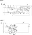
- Fig. 1A shows an example of the circuit arrangement for detecting and suppressing single-phase AC inputs.
- the input-side circuit includes a zero-crossing detector 10 with a comparator, a rectifier 3 and a current-limiting resistor 5 as well as circuits for the inputs, here for example an AC-voltage signal Ik (also called input, input signal, AC voltage signal or AC input signal) with a rectifier 4, a Voltage divider 6 and a comparator 8.
- the output signals are each a comparator signal S1 and a detector signal S2.
- the logic circuit 19 (also called logic block) comprises two timers 12a, 12b with the delay times Tva and TVb, two flip-flops 14a, 14b (for example implemented as bistable flip-flops), an exclusive OR gate 15a (also XOR gate or exclusive OR referred to), a multiplexer 16a and a controlled switch 18 (also called selector switch) between AC and DC operation.
- the circuit arrangement is designed to process an AC input signal (sinusoidal alternating voltage signal) and a DC input signal (direct voltage signal).
- the AC input signal comes from phase L of a supply network.
- the DC input signal comes from a DC source +Us. N or 0V denotes the neutral conductor (for AC) or the reference potential (for DC).
- the circuit arrangement is used, for example, in a programmable logic controller, a logic relay or similar.
- the detector signal S2 which can also be referred to as a zero crossing signal, is generated from phase L of the device by the zero crossing detector 10.
- the zero crossing detector 10 is constructed in the form of a comparator that compares the supply voltage with a ground potential GND (zero reference) or an approximate ground potential.
- the zero crossing detector detects 10 zero crossings and thus recognizes the applied AC input signal. In this case, the zero crossing detector 10 generates the detector signal S2. The detector signal S2 then triggers the timer 12a, which generates the clock signal S3a. If, on the other hand, there is a DC input signal, the zero crossing detector 10 does not detect any zero crossings. In this case, the zero crossing detector 10 does not generate the detector signal S2. The timer 12a is also not triggered in this case and does not generate the clock signal S3a.
- the supply voltage (input signal) at phase L is first rectified before being fed into the zero crossing detector 10.
- Fig. 1A illustrated schematically in the form of the diode 3.
- a resistor 5 with the value R3 can be arranged between the diode 3 and the zero crossing detector 10.
- the diode 3, for example, carries out half-wave rectification, so that the detector signal S2 can be generated from the signal obtained therefrom by the zero-crossing detector 10.
- the zero crossing detector 10 is implemented as a comparator.
- the input signal Ik is rectified by the rectifier 4, divided down by the voltage divider 6 (also called a step-down converter, here in the form of a simple voltage divider with two resistors R1, R2) and compared by the comparator 8 with a predefined threshold value Uth and thus as a comparator signal S1 "digitized".
- the input signal Ik is a voltage signal.
- the rectifier has a diode 4, which can be implemented discretely.
- Reference voltage source not shown, specifies the threshold value Uth.
- the threshold value Uth can be constant, for example.
- the changeover switch 18 remains in an upper position (DC operation). In this position of the switch 18, the output of the comparator 8 (at which the comparator signal S1 is generated) is connected directly to the output S7 of the circuit arrangement. The comparator signal S1 is therefore present at the output S7. If there is a DC input signal, it can be monitored by the comparator 8. If the DC input signal exceeds the predetermined threshold value Uth, the comparator 8 generates the comparator signal S1 and outputs it directly at the output S7 via the changeover switch 18.
- the changeover switch 18 switches - triggered by the zero crossing detector 10 or the timer 12a (eg via the detector signal S2, the clock signal S3 or another control signal, see dashed line in Fig. 1A ) - on the in Fig. 1A lower position shown (AC operation).
- the output of the comparator 8 ie the comparator signal S1 is fed to the data input D of the flip-flop 14a.
- the clock input Clk is controlled by the generated clock signal S3a.
- the components 12a, 12b, 14a, 14b, 15a, 16a and 18 are in the exemplary embodiment Fig. 1A implemented in a microcontroller that implements the logic circuit 19.
- the first comparator signal S1 is fed to an input of the microcontroller.
- the detector signal S2 is fed to an interrupt input of the microcontroller.
- the timing element 12a Starting from the detector signal S2, the timing element 12a generates the clock signal S3a as a clock for the flip-flop 14a.
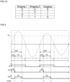
- the clock signal S3a has a defined change of state (falling clock edge, see Fig. 2 ), which occurs after a delay of T/8 of a period T after a zero crossing of the AC input signal Ik (detected by the detector signal S2).
- the timer 12b generates the clock signal S3b as a clock for the flip-flop 14b.
- the clock signal S3b has a state change (falling clock edge, see Fig. 2 ), which occurs after a delay of 3T/8 of a period T after a zero crossing of the AC input signal Ik. At these points in time, the effective value of the sinusoidal AC input signal Ik is present.
- the sinusoidal AC input signal corresponds to Ik.
- the clock signal S3a triggers the flip-flop 14a at its edge-controlled input Clk, with the value of the comparator signal S1 at the data input D of the flip-flop 14a being adopted at the respective time of a corresponding state change (falling clock edge) of the clock signal S3a (at T/8). and thus a first status signal S4a is generated at the output of the flip-flop 14a.
- a rising clock edge can also be used instead of a falling clock edge.
- the clock signal S3b triggers the flip-flop 14b at its edge-controlled input Clk, with the value of the comparator signal S1 at the data input D of the flip-flop 14b being taken over at the respective time of a corresponding state change (falling clock edge) of the clock signal S3a (at 3T/8). is and thus a second status signal S4b is generated at the output of the flip-flop 14b.
- an AC voltage status signal is provided at the output S7 and can be further processed, for example by a logic circuit of the electronic device (not shown) in which the circuit arrangement is used.
- the comparator signal S1 of the comparator 8 is always “0” and the value "0" is stored in the flip-flops 14a, 14b at any time. If there is a valid input signal Ik that exceeds the comparison threshold (threshold value Uth) of the comparator 8, the comparator signal S1 has a pulse. In the case of a sinusoidal AC input signal Ik, the pulse of the comparator signal S1 is um centers the peak of the input signal Ik, the width of which depends on the actual amplitude of the AC input signal Ik, ie the higher the amplitude, the wider the pulse of the comparator signal S1.
- the AC input signal Ik can thus be evaluated with regard to its effective value.
- Fig. 1B shows an alternative example of the circuit arrangement, which is a further development of the in Fig. 1A example shown.
- an applied input signal Ik is first fed to the step-down converter 6.
- the output signal of the step-down converter 6 is rectified by a first and a second diode 4a, 4b.
- the first diode 4a connects the input of the comparator 8 to a supply voltage connection.
- a supply voltage Vdd is present at the supply voltage connection.
- the first diode 4a is polarized such that a voltage at the input of the comparator 8 is smaller than the supply voltage Vdd (possibly plus a threshold voltage of the first diode 4a).
- the second diode 4b connects the input of the comparator 8 to a ground potential connection to which the ground potential GND is applied.
- the second diode 4b is polarized such that the voltage at the input of the comparator 8 is greater than the ground potential GND (possibly minus a threshold voltage of the second diode 4b).
- the comparator 8 can be implemented as a bipolar comparator.
- the comparator 8 generates the comparator signal S1 depending on a comparison of the voltage at the input Comparator 8 and the threshold value Uth.
- the comparator signal S1 is pulse-shaped.
- the pulse of the comparator signal S1 is recorded in time by the logic circuit 19, as in Fig. 1a specified.
- the comparator 8 can be implemented as an inverter.
- the diodes 4a, 4b can be integrated in the inverter, for example.
- the diodes 4a, 4b can be implemented as protective diodes.
- the inverter has a “built-in” threshold Uth.
- the first and second diodes 4a, 4b can optionally be integrated together with the inverter on a semiconductor body (e.g. a CMOS inverter of the HC04 type).
- an applied input signal Ik is first supplied to the resistor 5 with the value R3 and then rectified by a first and a second diode 3a, 3b.
- the first diode 3a connects the input of the zero crossing detector 10 to the supply voltage connection.
- the first diode 3a is polarized such that a voltage at the input of the zero crossing detector 10 is smaller than the supply voltage Vdd (possibly plus a threshold voltage of the first diode 3a).
- the second diode 3b connects the input of the zero crossing detector 10 to the ground potential connection.
- the second diode 3b is polarized such that the voltage at the input of the zero crossing detector 10 is greater than the ground potential GND (possibly minus a threshold voltage of the second diode 3b).
- the detector signal S2 is pulse-shaped.
- the zero crossing detector 10 can be implemented as a bipolar comparator.
- the zero crossing detector 10 can be implemented as an inverter.
- the diodes 3a, 3b can be integrated in the inverter, for example.
- the diodes 3a, 3b can be implemented as protective diodes.
- the zero crossing detector 10 has a “built-in” threshold. Since the voltage supplied to the zero crossing detector 10 is not divided down, the voltage rise is rapid. The time offset between the zero crossing of the supplied voltage and the switching of the zero crossing detector 10 is very small and can be neglected.
- the threshold value of the zero crossing detector 10 can be 0 V (i.e. the ground potential, as in Fig. 1B ) or a voltage other than 0 V, e.g. a small positive voltage (e.g. 2 V).
- the comparator 8 and/or the zero-crossing detector 10 can be implemented as a CMOS gate, e.g. a CMOS gate of type HC, or as a transistor.
- the resistance values of the resistors R1, R2 of the buck converter 6 are then dimensioned accordingly. Only the second diodes 4b and 3b can then be provided. The first diodes 4a and 3a can be omitted.
- the comparator 8 can be manufactured as a component to which the diodes 4a, 4b are connected externally as protective diodes, or as a component with integrated diodes 4a, 4b (such as a CMOS inverter with protective diodes such as HC04).
- the zero crossing detector 10 can be manufactured as a component to which the diodes 3a, 3b are connected externally as protective diodes, or as a component with integrated diodes 3a, 3b (such as a CMOS inverter with protective diodes such as HC04).
- the protective diodes can be protective diodes against electrostatic charging, abbreviated as ESD protective diodes.
- Pre-processing (rectification, step-down) is in Figures 1A and 1B shown exclusively as an example and can also be implemented with alternative circuits. Rectification can be omitted if necessary.
- the preprocessing is designed to protect the comparator 8 and/or the zero crossing detector 10 against overvoltages and undervoltages. This function can optionally also be performed by a rectifier diode 3b, 4b for negative undervoltages. If necessary, additional protection against overvoltage can be provided.
- Fig. 2 shows the sinusoidal input signal.
- the two acquisition times during the positive half-wave at which the signal has the same amplitude are T/8 (or 45°, or n/4) and 3T/8 (or 135°, or 3n/4).
- the signal is recorded at both points in time. Normally, the values are either both 1 or both 0, depending on the amplitude of the input signal Ik, as in the first or second period T in Fig. 2 .
- the detector signal S2 also called the zero crossing signal, triggers with the first edge (e.g. the positive in Fig. 2 ) the first timer 12a, which generates a pulse S3a with a duration of T/8.
- the second edge e.g. the negative edge in Fig. 2
- the comparator signal S1 which represents the digitized input signal
- the stored status signals S4a, S4b of the flip-flops 14a, 14b are compared with one another by the XOR gate 15a.
- the suppression works in the same way if the second acquisition in 3T/8 is corrupted.
- the disclosure primarily concerns AC operation.
- a controllable switch 18 between AC and DC operation can optionally be provided at the output of the logic circuit 19.
- the comparator signal S1 for DC operation or the first output signal S41 for AC operation is switched on at output S7.
- the control is carried out by an in Fig. 1 Circuit, not shown, from detector signal S2 (or one of the talk signals S3a, S3b).
- these signals are pulse-shaped; in the case of DC supply, they are static.
- the pulses could, for example, control a retriggerable monoflop (monostable flip-flop) and thus differentiate between AC (output active) and DC (output inactive).
- the logic circuit (also called logic block) can be implemented, for example, in the firmware of a microcontroller.
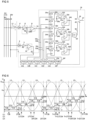
- Fig. 5 shows an example of the circuit arrangement for detecting and suppressing three-phase AC inputs.
- the input-side circuit includes the zero-crossing detector with, for example, the rectifier 3, the current-limiting resistor 5 and the comparator 10, as well as circuits for the inputs, shown here as an example for an input signal Ik with the rectifier 4, the voltage divider 6 and the comparator 8.
- the output signals are the comparator signal S1 and the detector signal S2.
- the logic block 19 includes six timers "Tv1a” 12a, “TV1b” 12b, “Tv2a” 12c, “TV2b” 12d, “Tv3a” 12e, “TV3b” 12f, six flip-flops (bistable flip-flops) 14a, 14b, 14c, 14d, 14e, 14f, three XOR gates (exclusive or) 15a, 15b, 15c, three multiplexers 16a, 16b, 16c, an OR gate 20 with three inputs and the controlled switch 18 between AC and DC operation.
- the input signal Ik is not recorded in the peak point (T/4), but in T/8 and, for interference suppression, also in 3T/8 of the respective phase.
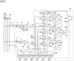
- a single timer can be used for the firmware implementation because, starting from the zero crossing of the supply phase (detector signal S2), none of the timers run simultaneously.
- timing elements can also be arranged in parallel with correspondingly calculated times. This would not be a problem for a hardware implementation, but would be disadvantageous for an implementation in the firmware of a microcontroller because six separate timers would be required.
- the timers Tvla, Tvlb, TV2a, Tv2b, Tv3a, Tv3b are triggered in such a way that the clock signals S3a to S3f switch exactly at the previously described detection times. These are each fed to a flip-flop 14a to 14f to the clock input.
- the comparator signal S1 is present at the data input D. In this way, the state of the comparator signal S1 at the respective time is stored in the flip-flops 14a to 14f.
- first and second status signals S4a, S4b for the first phase “La” supply phase, eg L1
- the third and the fourth status signal S4c, S4d for the second phase "Lb” eg L2
- the fifth and sixth status signals S4e, S4f for the third phase "Lc” eg L3
- the two signals for each phase are compared with one another by the If the two status signals are the same, the value is adopted as the first, second and third output signals S41, S42, S43, if not the previous value of the output signal S41, S42, S43 is retained.
- the output signals S41, S42, S43 are processed by the OR gate 20 and an AC voltage state signal S6 is generated at the output of the OR gate 20 and from this the output signal is generated at the output S7.
- the outputs of the first and last timers 12f, 12e are connected to the flip-flops 14e, 14f.
- the outputs of the second and third timers 12a, 12b are connected to the flip-flops 14a, 14b and the outputs of the fourth and fifth timers 12c, 12d are connected to the flip-flops 14c, 14d.
- a timer in the microcontroller, which implements the logic circuit 19, is advantageously sufficient.
- a controllable switch 18 between AC and DC operation can be provided at the output of the logic circuit 19.
- the comparator signal S1 for DC operation or the alternating voltage status signal S6 for AC operation is switched on at output S7.
- the control is carried out by an in Fig. 5 or. Fig. 7 Circuit, not shown, from the detector signal S2 or from one of the clock signals S3a to S3f.
- these signals are pulse-shaped; in the case of DC supply, they are static.
- the pulses could, for example, control a retriggerable monoflop (monostable flip-flop) and thus differentiate between AC (output active) and DC (output inactive).
- the logic block 19 is implemented in the firmware of a microcontroller.
- a timer can be referred to as a timer.
- An interruption can also be called an interrupt.
- Figure 12 shows a table indicating a method of single-phase firmware implementation.
- the table describes the procedure for detecting and suppressing single-phase inputs, cf. Fig. 1A .
- Figure 13 shows a table that explains a method for firmware implementation three-phase with two timers.
- the table describes the procedure for detecting and suppressing three-phase inputs with two microcontroller-internal timers, cf. Fig. 5 .
- the two timers could alternatively be used one after the other or arbitrarily, the only restriction is that the time from time 0 and the last time from 19T/24 would have to be implemented with different timers, because they sometimes run at the same time.
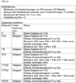
- Figure 14 shows a table that specifies a method for firmware implementation three-phase with exactly one timer.
- the table describes the procedure for detecting and suppressing three-phase inputs with a microcontroller-internal timer, cf. Fig. 7 .
- Figures 15A to 15C show an example of a detail of the circuit arrangement shown above and signals of the circuit arrangement. So that a hardware circuit like in Fig. 1A shown with the multiplexer functioning correctly, an additional delay (eg an RC element) can be provided between the output of the second flip-flop 14b, at which the second status signal S4b is provided, and the input "0" of the multiplexer 16a.
- an additional delay eg an RC element
- Delay element 25 is arranged between the output of the second flip-flop 14b and the input "0" of the multiplexer 16a.
- the delay element 25 can be implemented as a filter, for example as a low pass or RC element, or as an inverter connected in series.
- the correct function in the event of a signal change is ensured by supplying the second status signal S4b and not the first status signal S4a to input 0 of the multiplexer 16a. If the state of the comparator signal S1 changes (from 0 to 1 or from 1 to 0), the first state signal S4a switches and only after T/4 does the second state signal S4b switch. The change of state from the first state signal S4a switches the multiplexer 16a to input "1" through the first processing signal S51, while the second state signal S4b is still stable at the old value, namely the same as the first output signal S41. This means there are no problems when switching over; the old value is initially retained. If after T/4 the second status signal S4b also assumes the new value, the multiplexer 16a switches to input "0" and the new value is passed on as the first output signal S41.
- FIG. 15B explains a functional diagram without delay of the second status signal S4b.
- the second status signal S5 is delayed by the XOR gate 15a (exaggerated here).
- the disturbance of the second status signal S4b is not eliminated because the disturbed second status signal S4b arrives at the multiplexer input "0" faster than the multiplexer 16a switches over.
- FIG. 15C explains a functional diagram with delay of the second status signal S4b.
- the first processing signal S51 is delayed by the XOR gate 15a, but that The disturbed second status signal S4b is delayed even longer to the multiplexer input "0" (exaggerated here).
- the interference with the second status signal S4b is eliminated.
- a small wiper towards 0 is created at the "end of the disturbance".
- the delays are in reality very small (in the 10 ns to 100 ns range) and the wiper is problem-free with additional filtering of the first Output signal S41 is ironed out, ie eliminated.
- the illustrated embodiments represent exemplary embodiments of the improved circuit arrangement and method, and therefore do not represent a complete list of all embodiments of the improved circuit arrangement.
- the actual configurations of the circuit arrangement may differ from the embodiments, for example with respect to circuit parts, method steps or circuit parameters such as delay times being represented.
Landscapes
- Physics & Mathematics (AREA)
- Engineering & Computer Science (AREA)
- General Physics & Mathematics (AREA)
- Power Engineering (AREA)
- Computer Hardware Design (AREA)
- Computing Systems (AREA)
- General Engineering & Computer Science (AREA)
- Mathematical Physics (AREA)
- Nonlinear Science (AREA)
- Inverter Devices (AREA)
- Measurement Of Current Or Voltage (AREA)
- Manipulation Of Pulses (AREA)
Claims (10)
- Système de circuit destiné à surveiller un signal (Ik) sous forme de tension alternative, comprenant :- un comparateur (8), auquel peut être appliqué, au niveau d'une première entrée de comparateur, le signal (Ik) sous forme de tension alternative ou un signal obtenu à partir de celui-ci et qui est conçu pour émettre, au niveau d'une sortie de comparateur, un signal de comparateur (S1) en fonction d'une comparaison du signal (Ik) sous forme de tension alternative ou du signal obtenu à partir de celui-ci à une valeur seuil (Uth) définie,- un détecteur de passage par zéro (10), auquel peut être appliqué, au niveau d'une entrée de surveillance, un signal de référence ou un signal obtenu à partir de celui-ci et qui est conçu pour générer, au niveau d'une sortie du détecteur de passage par zéro (10), un signal de détecteur (S2) et- un circuit logique (19),le signal de référence étant sous forme de tension alternative et le signal de référence et le signal (Ik) sous forme de tension alternative étant de même fréquence,le circuit logique (19) comprenant :- un premier temporisateur (12a) monté en aval du détecteur de passage par zéro (10) et destiné à générer un premier signal d'horloge (S3a) en fonction du signal de détecteur (S2),- un deuxième temporisateur (12b) monté en aval du détecteur de passage par zéro (10) et destiné à générer un deuxième signal d'horloge (S3b) en fonction du signal de détecteur (S2) ou en fonction du premier signal d'horloge (S3a),- une première et une deuxième bascule bistable (14a, 14b) et- une porte OU exclusive (15a),une sortie du comparateur (8) étant couplée à une entrée de données (D) de la première bascule bistable (14a) et de la deuxième bascule bistable (14b),une sortie du premier temporisateur (12a) étant couplée à une entrée d'horloge de la première bascule bistable (14a) et une sortie du deuxième temporisateur (12b) étant couplée à une entrée d'horloge de la deuxième bascule bistable (14b),une sortie de la première bascule bistable (14a) et une sortie de la deuxième bascule bistable (14b) étant couplée à des entrées de la porte OU exclusive (15a),la porte OU exclusive (15a) étant conçue pour générer un premier signal de transformation (S51),le circuit logique (19) étant conçu pour échantillonner le signal de comparateur (S1) en au moins deux moments spécifiés et générer le premier signal de transformation (S51) avec une première valeur lorsque, en au moins deux moments déterminés des au moins deux moments spécifiés, le signal de comparateur (S1) présente des valeurs différentes et avec une deuxième valeur lorsque, en les deux moments déterminés, le signal de comparateur (S1) présente la même valeur etles deux moments déterminés des au moins deux moments spécifiés se situant aux valeurs suivantes :
 T représentant une durée de période du signal (Ik) sous forme de tension alternative à surveiller et Δt représentant une durée inférieure à T/4.
 - Système de circuit selon la revendication 1,
le circuit logique (19) étant conçu pour- générer, à la deuxième valeur du premier signal de transformation (S51), un premier signal de sortie (S41) qui présente la valeur de la valeur du signal de comparateur (S1) échantillonné aux deux moments déterminés et- conserver, à la première valeur du premier signal de transformation (S51), la valeur antérieure du premier signal de sortie (S41). - Système de circuit selon la revendication 1 ou 2,le circuit logique (19) étant conçu pour générer un deuxième signal de transformation (S52) avec une première valeur lorsque, en deux autres moments déterminés des au moins deux moments spécifiés, le signal de comparateur (S1) présente des valeurs différentes et avec une deuxième valeur lorsque, en les deux autres moments déterminés, le signal de comparateur (S1) présente la même valeur etle circuit logique (19) étant conçu pour générer un troisième signal de transformation (S53) avec une première valeur lorsque, en deux moments déterminés supplémentaires des au moins deux moments spécifiés, le signal de comparateur (S1) présente des valeurs différentes et avec une deuxième valeur lorsque, en les deux moments déterminés supplémentaires, le signal de comparateur (S1) présente la même valeur.
- Système de circuit selon la revendication 3,
le circuit logique (19) étant conçu pour- générer, à la deuxième valeur du deuxième signal de transformation (S52), un deuxième signal de sortie (S42) qui présente la valeur de la valeur du signal de comparateur (S1) échantillonné en les deux autres moments déterminés et- conserver, à la première valeur du deuxième signal de transformation (S52), la valeur antérieure du deuxième signal de sortie (S42),- générer, à la deuxième valeur du troisième signal de transformation (S53), un troisième signal de sortie (S43) qui présente la valeur de la valeur du signal de comparateur (S1) échantillonné en les deux moments déterminés supplémentaires et- conserver, à la première valeur du troisième signal de transformation (S53), la valeur antérieure du troisième signal de sortie (S43) et générer un signal d'état de tension alternative (S6) par liaison OU du premier, du deuxième et du troisième signal de sortie (S41, S42, S43). - Système de circuit selon l'une des revendications 1 à 4, le circuit logique (19) étant réalisé comme un microcontrôleur ou un microprocesseur.
- Système de circuit selon l'une des revendications 1 à 5, le deuxième temporisateur (12b) étant monté en aval du premier temporisateur (12a) et étant conçu pour être déclenché par le premier signal d'horloge (S3a) afin de générer le deuxième signal d'horloge (S3b).
- Système de circuit selon l'une des revendications 1 à 6, le circuit logique (19) comprenant un multiplexeur (16a) et le multiplexeur (16a) présentant :- une première entrée, qui est couplée à la sortie de la première ou de la deuxième bascule bistable (14a, 14b),- une deuxième entrée,- une entrée de commande, qui est couplée à une sortie de la porte OU exclusive (15a) et- une sortie, qui est couplée à la deuxième entrée et qui est conçue pour émettre le premier signal de sortie (S41).
- Système de circuit selon la revendication 7, le multiplexeur (16a), la porte OU exclusive (15a), les bascules bistables (14a, 14b) et les temporisateurs (12a, 12b) étant réalisés par des logiciels au sein d'un microcontrôleur ou d'un microprocesseur.
- Système de circuit selon l'une des revendications 1 à 8, les deux moments déterminés étant T/8 et T·3/8.
- Procédé destiné à surveiller un signal (Ik) sous forme de tension alternative, comprenant :- la détection du signal (Ik) en forme de tension alternative,- la génération d'un signal de comparateur (S1) par un comparateur (8) en fonction d'une comparaison du signal (Ik) en forme de tension alternative ou du signal obtenu à partir de celui-ci à une valeur seuil définie (Uth),- la génération d'un signal de détecteur (S2) par un détecteur de passage par zéro (10), auquel un signal de référence ou un signal obtenu à partir de celui-ci est appliqué et- l'échantillonnage du signal de comparateur (S1) en au moins deux moments spécifiés et génération d'un premier signal de transformation (S51) avec une première valeur lorsque, en deux moments déterminés des au moins deux moments spécifiés, le signal de comparateur (S1) présente des valeurs différentes et avec une deuxième valeur lorsque, en les deux moments déterminés, le signal de comparateur (S1) présente la même valeur,le signal de référence étant sous forme de tension alternative et le signal de référence et le signal (Ik) sous forme de tension alternative étant de même fréquence,les deux moments déterminés des au moins deux moments spécifiés se situant aux valeurs suivantes :
 T représentant une durée de période du signal (Ik) sous forme de tension alternative à surveiller et Δt représentant une durée inférieure à T/4,un circuit logique (19) comprenant :- un premier temporisateur (12a) monté en aval du détecteur de passage par zéro (10) et destiné à générer un premier signal d'horloge (S3a) en fonction du signal de détecteur (S2),- un deuxième temporisateur (12b) monté en aval du détecteur de passage par zéro (10) et destiné à générer un deuxième signal d'horloge (S3b) en fonction du signal de détecteur (S2) ou en fonction du premier signal d'horloge (S3a),- une première et une deuxième bascule bistable (14a, 14b) et- une porte OU exclusive (15a),une sortie du comparateur (8) étant couplée à une entrée de données (D) de la première bascule bistable (14a) et de la deuxième bascule bistable (14b),une sortie du premier temporisateur (12a) étant couplée à une entrée d'horloge de la première bascule bistable (14a) et une sortie du deuxième temporisateur (12b) étant couplée à une entrée d'horloge de la deuxième bascule bistable (14b),une sortie de la première bascule bistable (14a) et une sortie de la deuxième bascule bistable (14b) étant couplées à des entrées de la porte OU exclusive (15a) etla porte OU exclusive (15a) générant le premier signal de transformation (S51).
Applications Claiming Priority (2)
| Application Number | Priority Date | Filing Date | Title |
|---|---|---|---|
| DE102019107641.2A DE102019107641A1 (de) | 2019-03-25 | 2019-03-25 | Schaltungsanordnung und Verfahren zur Überwachung eines wechselspannungsförmigen Signals |
| PCT/EP2020/057260 WO2020193282A1 (fr) | 2019-03-25 | 2020-03-17 | Circuit et procédé de surveillance d'un signal de tension alternative |
Publications (2)
| Publication Number | Publication Date |
|---|---|
| EP3948311A1 EP3948311A1 (fr) | 2022-02-09 |
| EP3948311B1 true EP3948311B1 (fr) | 2023-11-15 |
Family
ID=69846116
Family Applications (1)
| Application Number | Title | Priority Date | Filing Date |
|---|---|---|---|
| EP20712310.0A Active EP3948311B1 (fr) | 2019-03-25 | 2020-03-17 | Circuit et procédé de surveillance d'un signal de tension alternative |
Country Status (6)
| Country | Link |
|---|---|
| US (1) | US12088305B2 (fr) |
| EP (1) | EP3948311B1 (fr) |
| CN (1) | CN113826017B (fr) |
| DE (1) | DE102019107641A1 (fr) |
| PL (1) | PL3948311T3 (fr) |
| WO (1) | WO2020193282A1 (fr) |
Families Citing this family (3)
| Publication number | Priority date | Publication date | Assignee | Title |
|---|---|---|---|---|
| DE102021127228A1 (de) | 2021-10-20 | 2023-04-20 | Northrop Grumman Litef Gmbh | Elektrisches Gerät mit indirektem Blitzschutz, Kurs-Lage-Referenz-System und Flugzeug |
| CN117250401A (zh) * | 2023-09-21 | 2023-12-19 | 上海裕芯电子科技有限公司 | 一种交流相位检测装置 |
| TWI869294B (zh) * | 2024-06-05 | 2025-01-01 | 神雲科技股份有限公司 | 多主控端控制電路 |
Family Cites Families (9)
| Publication number | Priority date | Publication date | Assignee | Title |
|---|---|---|---|---|
| US3611162A (en) * | 1970-07-09 | 1971-10-05 | Yokogawa Electric Works Ltd | Apparatus for detecting abnormal conditions of ac sources |
| CN1126957C (zh) * | 1997-11-04 | 2003-11-05 | 默勒有限公司 | 用于监测交变电压型信号的确定幅度阈值的方法及电路装置 |
| JP2001133489A (ja) * | 1999-11-04 | 2001-05-18 | Yokogawa Electric Corp | Rms測定装置 |
| JP5015576B2 (ja) | 2006-03-15 | 2012-08-29 | 株式会社豊田中央研究所 | 2値化回路 |
| CN105759157A (zh) * | 2016-05-13 | 2016-07-13 | 魏德米勒电联接(上海)有限公司 | 交直流信号检测系统及交流信号有效值的测量方法 |
| CN207164127U (zh) * | 2017-07-07 | 2018-03-30 | 佛山科学技术学院 | 一种数字输出的电压峰值检测电路 |
| DE102017116534A1 (de) * | 2017-07-21 | 2019-01-24 | Eaton Electrical Ip Gmbh & Co. Kg | Schaltungsanordnung und Verfahren zur Überwachung wechselspannungsförmiger Signale |
| CN207765960U (zh) * | 2017-10-18 | 2018-08-24 | 深圳市赛源电气技术有限公司 | 过零检测电路及电容补偿柜 |
| DE102017127070A1 (de) * | 2017-11-17 | 2019-05-23 | Eaton Electrical Ip Gmbh & Co. Kg | Schaltungsanordnung und Verfahren zur Überwachung wechselspannungsförmiger Signale |
-
2019
- 2019-03-25 DE DE102019107641.2A patent/DE102019107641A1/de not_active Withdrawn
-
2020
- 2020-03-17 WO PCT/EP2020/057260 patent/WO2020193282A1/fr not_active Ceased
- 2020-03-17 CN CN202080036004.9A patent/CN113826017B/zh active Active
- 2020-03-17 PL PL20712310.0T patent/PL3948311T3/pl unknown
- 2020-03-17 US US17/442,143 patent/US12088305B2/en active Active
- 2020-03-17 EP EP20712310.0A patent/EP3948311B1/fr active Active
Also Published As
| Publication number | Publication date |
|---|---|
| CN113826017A (zh) | 2021-12-21 |
| EP3948311A1 (fr) | 2022-02-09 |
| DE102019107641A1 (de) | 2020-10-01 |
| PL3948311T3 (pl) | 2024-05-06 |
| US12088305B2 (en) | 2024-09-10 |
| CN113826017B (zh) | 2024-05-24 |
| WO2020193282A1 (fr) | 2020-10-01 |
| US20220224319A1 (en) | 2022-07-14 |
Similar Documents
| Publication | Publication Date | Title |
|---|---|---|
| EP3948311B1 (fr) | Circuit et procédé de surveillance d'un signal de tension alternative | |
| EP3711160B1 (fr) | Agencement de circuit et procédé de surveillance de signaux sinusoïdaux de tension alternative | |
| DE3327188A1 (de) | Selbstpruefender naeherungsschalter | |
| EP2887163B1 (fr) | Dispositif de surveillance, système de sécurité et procédé de fonctionnement d'un système de sécurité | |
| EP3745596B1 (fr) | Circuit d'entrée numérique permettant de recevoir des signaux d'entrée numérique d'au moins un émetteur de signaux | |
| EP3655785B1 (fr) | Système de circuit et procédé de surveillance de signaux sous forme de tension alternative | |
| EP0328093A2 (fr) | Convertisseur de code de gray avec signal de défaut | |
| EP0775332A1 (fr) | Ensemble commutateur de securite | |
| DE102012205289B4 (de) | Verfahren zum Betreiben eines Sicherheitssensors | |
| DE102019113139A1 (de) | Vorrichtung und Verfahren zur Stromsteuerung eines Aktuators | |
| EP1900088B1 (fr) | Dispositif circuit pour determiner les passages par zero d'une tension alternative | |
| EP0898368A2 (fr) | Dispositif capteur | |
| EP3404430B1 (fr) | Procédé de surveillance du fonctionnement d'une interface binaire et interface binaire correspondante | |
| DE4403156B4 (de) | Verfahren und Vorrichtung zur Durchführung des Verfahrens zur Ansteuerung eines Verbrauchers | |
| EP2117094B1 (fr) | Commutation de surveillance et procédé de contrôle d'une commutation | |
| EP0270871A2 (fr) | Système pour l'entrée/sortie de signaux dans un système de commande digitale | |
| DE19733733C2 (de) | Verfahren und Schaltungsanordnung zur Bearbeitung digitaler Signale | |
| DE102012012115A1 (de) | Verfahren zur Erkennung von elektromagnetischen Strörinpulsen und Elektronikbauteil zur Durchführung des Verfahrens | |
| EP2733718B1 (fr) | Procédé et dispositif d'évaluation de signaux provenant d'un élément de sortie OSSD | |
| DE3527619C1 (de) | Selbstprüfender Näherungsschalter | |
| DE3342710C1 (de) | Näherungsschalter mit Überwachung der Funktion und Funktionsbereitschaft | |
| LU103339B1 (de) | Auswerteeinheit für Näherungsschalter | |
| EP2988419A1 (fr) | Procede de determination de l'etat d'un element indicateur formant un court-circuit | |
| DE3326283A1 (de) | Einrichtung zur ueberwachung hoher wechselspannungen | |
| DE2822562C2 (de) | Anordnung zur Erfassung von Störungen bei Stromrichtern |
Legal Events
| Date | Code | Title | Description |
|---|---|---|---|
| STAA | Information on the status of an ep patent application or granted ep patent |
Free format text: STATUS: UNKNOWN |
|
| STAA | Information on the status of an ep patent application or granted ep patent |
Free format text: STATUS: THE INTERNATIONAL PUBLICATION HAS BEEN MADE |
|
| PUAI | Public reference made under article 153(3) epc to a published international application that has entered the european phase |
Free format text: ORIGINAL CODE: 0009012 |
|
| STAA | Information on the status of an ep patent application or granted ep patent |
Free format text: STATUS: REQUEST FOR EXAMINATION WAS MADE |
|
| 17P | Request for examination filed |
Effective date: 20211025 |
|
| AK | Designated contracting states |
Kind code of ref document: A1 Designated state(s): AL AT BE BG CH CY CZ DE DK EE ES FI FR GB GR HR HU IE IS IT LI LT LU LV MC MK MT NL NO PL PT RO RS SE SI SK SM TR |
|
| DAV | Request for validation of the european patent (deleted) | ||
| DAX | Request for extension of the european patent (deleted) | ||
| GRAP | Despatch of communication of intention to grant a patent |
Free format text: ORIGINAL CODE: EPIDOSNIGR1 |
|
| STAA | Information on the status of an ep patent application or granted ep patent |
Free format text: STATUS: GRANT OF PATENT IS INTENDED |
|
| P01 | Opt-out of the competence of the unified patent court (upc) registered |
Effective date: 20230521 |
|
| INTG | Intention to grant announced |
Effective date: 20230612 |
|
| GRAS | Grant fee paid |
Free format text: ORIGINAL CODE: EPIDOSNIGR3 |
|
| GRAA | (expected) grant |
Free format text: ORIGINAL CODE: 0009210 |
|
| STAA | Information on the status of an ep patent application or granted ep patent |
Free format text: STATUS: THE PATENT HAS BEEN GRANTED |
|
| AK | Designated contracting states |
Kind code of ref document: B1 Designated state(s): AL AT BE BG CH CY CZ DE DK EE ES FI FR GB GR HR HU IE IS IT LI LT LU LV MC MK MT NL NO PL PT RO RS SE SI SK SM TR |
|
| REG | Reference to a national code |
Ref country code: CH Ref legal event code: EP Ref country code: GB Ref legal event code: FG4D Free format text: NOT ENGLISH |
|
| REG | Reference to a national code |
Ref country code: DE Ref legal event code: R096 Ref document number: 502020006035 Country of ref document: DE |
|
| REG | Reference to a national code |
Ref country code: IE Ref legal event code: FG4D Free format text: LANGUAGE OF EP DOCUMENT: GERMAN |
|
| REG | Reference to a national code |
Ref country code: NL Ref legal event code: FP |
|
| REG | Reference to a national code |
Ref country code: LT Ref legal event code: MG9D |
|
| PG25 | Lapsed in a contracting state [announced via postgrant information from national office to epo] |
Ref country code: GR Free format text: LAPSE BECAUSE OF FAILURE TO SUBMIT A TRANSLATION OF THE DESCRIPTION OR TO PAY THE FEE WITHIN THE PRESCRIBED TIME-LIMIT Effective date: 20240216 |
|
| PG25 | Lapsed in a contracting state [announced via postgrant information from national office to epo] |
Ref country code: IS Free format text: LAPSE BECAUSE OF FAILURE TO SUBMIT A TRANSLATION OF THE DESCRIPTION OR TO PAY THE FEE WITHIN THE PRESCRIBED TIME-LIMIT Effective date: 20240315 |
|
| PG25 | Lapsed in a contracting state [announced via postgrant information from national office to epo] |
Ref country code: LT Free format text: LAPSE BECAUSE OF FAILURE TO SUBMIT A TRANSLATION OF THE DESCRIPTION OR TO PAY THE FEE WITHIN THE PRESCRIBED TIME-LIMIT Effective date: 20231115 |
|
| PG25 | Lapsed in a contracting state [announced via postgrant information from national office to epo] |
Ref country code: ES Free format text: LAPSE BECAUSE OF FAILURE TO SUBMIT A TRANSLATION OF THE DESCRIPTION OR TO PAY THE FEE WITHIN THE PRESCRIBED TIME-LIMIT Effective date: 20231115 |
|
| PG25 | Lapsed in a contracting state [announced via postgrant information from national office to epo] |
Ref country code: LT Free format text: LAPSE BECAUSE OF FAILURE TO SUBMIT A TRANSLATION OF THE DESCRIPTION OR TO PAY THE FEE WITHIN THE PRESCRIBED TIME-LIMIT Effective date: 20231115 Ref country code: IS Free format text: LAPSE BECAUSE OF FAILURE TO SUBMIT A TRANSLATION OF THE DESCRIPTION OR TO PAY THE FEE WITHIN THE PRESCRIBED TIME-LIMIT Effective date: 20240315 Ref country code: GR Free format text: LAPSE BECAUSE OF FAILURE TO SUBMIT A TRANSLATION OF THE DESCRIPTION OR TO PAY THE FEE WITHIN THE PRESCRIBED TIME-LIMIT Effective date: 20240216 Ref country code: ES Free format text: LAPSE BECAUSE OF FAILURE TO SUBMIT A TRANSLATION OF THE DESCRIPTION OR TO PAY THE FEE WITHIN THE PRESCRIBED TIME-LIMIT Effective date: 20231115 Ref country code: BG Free format text: LAPSE BECAUSE OF FAILURE TO SUBMIT A TRANSLATION OF THE DESCRIPTION OR TO PAY THE FEE WITHIN THE PRESCRIBED TIME-LIMIT Effective date: 20240215 Ref country code: PT Free format text: LAPSE BECAUSE OF FAILURE TO SUBMIT A TRANSLATION OF THE DESCRIPTION OR TO PAY THE FEE WITHIN THE PRESCRIBED TIME-LIMIT Effective date: 20240315 |
|
| PG25 | Lapsed in a contracting state [announced via postgrant information from national office to epo] |
Ref country code: SE Free format text: LAPSE BECAUSE OF FAILURE TO SUBMIT A TRANSLATION OF THE DESCRIPTION OR TO PAY THE FEE WITHIN THE PRESCRIBED TIME-LIMIT Effective date: 20231115 Ref country code: RS Free format text: LAPSE BECAUSE OF FAILURE TO SUBMIT A TRANSLATION OF THE DESCRIPTION OR TO PAY THE FEE WITHIN THE PRESCRIBED TIME-LIMIT Effective date: 20231115 Ref country code: NO Free format text: LAPSE BECAUSE OF FAILURE TO SUBMIT A TRANSLATION OF THE DESCRIPTION OR TO PAY THE FEE WITHIN THE PRESCRIBED TIME-LIMIT Effective date: 20240215 Ref country code: LV Free format text: LAPSE BECAUSE OF FAILURE TO SUBMIT A TRANSLATION OF THE DESCRIPTION OR TO PAY THE FEE WITHIN THE PRESCRIBED TIME-LIMIT Effective date: 20231115 Ref country code: HR Free format text: LAPSE BECAUSE OF FAILURE TO SUBMIT A TRANSLATION OF THE DESCRIPTION OR TO PAY THE FEE WITHIN THE PRESCRIBED TIME-LIMIT Effective date: 20231115 |
|
| PG25 | Lapsed in a contracting state [announced via postgrant information from national office to epo] |
Ref country code: DK Free format text: LAPSE BECAUSE OF FAILURE TO SUBMIT A TRANSLATION OF THE DESCRIPTION OR TO PAY THE FEE WITHIN THE PRESCRIBED TIME-LIMIT Effective date: 20231115 |
|
| PG25 | Lapsed in a contracting state [announced via postgrant information from national office to epo] |
Ref country code: CZ Free format text: LAPSE BECAUSE OF FAILURE TO SUBMIT A TRANSLATION OF THE DESCRIPTION OR TO PAY THE FEE WITHIN THE PRESCRIBED TIME-LIMIT Effective date: 20231115 |
|
| PG25 | Lapsed in a contracting state [announced via postgrant information from national office to epo] |
Ref country code: SK Free format text: LAPSE BECAUSE OF FAILURE TO SUBMIT A TRANSLATION OF THE DESCRIPTION OR TO PAY THE FEE WITHIN THE PRESCRIBED TIME-LIMIT Effective date: 20231115 |
|
| PG25 | Lapsed in a contracting state [announced via postgrant information from national office to epo] |
Ref country code: SM Free format text: LAPSE BECAUSE OF FAILURE TO SUBMIT A TRANSLATION OF THE DESCRIPTION OR TO PAY THE FEE WITHIN THE PRESCRIBED TIME-LIMIT Effective date: 20231115 Ref country code: SK Free format text: LAPSE BECAUSE OF FAILURE TO SUBMIT A TRANSLATION OF THE DESCRIPTION OR TO PAY THE FEE WITHIN THE PRESCRIBED TIME-LIMIT Effective date: 20231115 Ref country code: RO Free format text: LAPSE BECAUSE OF FAILURE TO SUBMIT A TRANSLATION OF THE DESCRIPTION OR TO PAY THE FEE WITHIN THE PRESCRIBED TIME-LIMIT Effective date: 20231115 Ref country code: EE Free format text: LAPSE BECAUSE OF FAILURE TO SUBMIT A TRANSLATION OF THE DESCRIPTION OR TO PAY THE FEE WITHIN THE PRESCRIBED TIME-LIMIT Effective date: 20231115 Ref country code: DK Free format text: LAPSE BECAUSE OF FAILURE TO SUBMIT A TRANSLATION OF THE DESCRIPTION OR TO PAY THE FEE WITHIN THE PRESCRIBED TIME-LIMIT Effective date: 20231115 Ref country code: CZ Free format text: LAPSE BECAUSE OF FAILURE TO SUBMIT A TRANSLATION OF THE DESCRIPTION OR TO PAY THE FEE WITHIN THE PRESCRIBED TIME-LIMIT Effective date: 20231115 |
|
| REG | Reference to a national code |
Ref country code: DE Ref legal event code: R097 Ref document number: 502020006035 Country of ref document: DE |
|
| PLBE | No opposition filed within time limit |
Free format text: ORIGINAL CODE: 0009261 |
|
| STAA | Information on the status of an ep patent application or granted ep patent |
Free format text: STATUS: NO OPPOSITION FILED WITHIN TIME LIMIT |
|
| 26N | No opposition filed |
Effective date: 20240819 |
|
| PG25 | Lapsed in a contracting state [announced via postgrant information from national office to epo] |
Ref country code: SI Free format text: LAPSE BECAUSE OF FAILURE TO SUBMIT A TRANSLATION OF THE DESCRIPTION OR TO PAY THE FEE WITHIN THE PRESCRIBED TIME-LIMIT Effective date: 20231115 |
|
| PG25 | Lapsed in a contracting state [announced via postgrant information from national office to epo] |
Ref country code: SI Free format text: LAPSE BECAUSE OF FAILURE TO SUBMIT A TRANSLATION OF THE DESCRIPTION OR TO PAY THE FEE WITHIN THE PRESCRIBED TIME-LIMIT Effective date: 20231115 |
|
| PG25 | Lapsed in a contracting state [announced via postgrant information from national office to epo] |
Ref country code: LU Free format text: LAPSE BECAUSE OF NON-PAYMENT OF DUE FEES Effective date: 20240317 |
|
| PG25 | Lapsed in a contracting state [announced via postgrant information from national office to epo] |
Ref country code: MC Free format text: LAPSE BECAUSE OF FAILURE TO SUBMIT A TRANSLATION OF THE DESCRIPTION OR TO PAY THE FEE WITHIN THE PRESCRIBED TIME-LIMIT Effective date: 20231115 |
|
| PG25 | Lapsed in a contracting state [announced via postgrant information from national office to epo] |
Ref country code: MC Free format text: LAPSE BECAUSE OF FAILURE TO SUBMIT A TRANSLATION OF THE DESCRIPTION OR TO PAY THE FEE WITHIN THE PRESCRIBED TIME-LIMIT Effective date: 20231115 Ref country code: LU Free format text: LAPSE BECAUSE OF NON-PAYMENT OF DUE FEES Effective date: 20240317 |
|
| REG | Reference to a national code |
Ref country code: BE Ref legal event code: MM Effective date: 20240331 |
|
| PG25 | Lapsed in a contracting state [announced via postgrant information from national office to epo] |
Ref country code: BE Free format text: LAPSE BECAUSE OF NON-PAYMENT OF DUE FEES Effective date: 20240331 |
|
| PG25 | Lapsed in a contracting state [announced via postgrant information from national office to epo] |
Ref country code: IE Free format text: LAPSE BECAUSE OF NON-PAYMENT OF DUE FEES Effective date: 20240317 |
|
| PG25 | Lapsed in a contracting state [announced via postgrant information from national office to epo] |
Ref country code: IE Free format text: LAPSE BECAUSE OF NON-PAYMENT OF DUE FEES Effective date: 20240317 Ref country code: BE Free format text: LAPSE BECAUSE OF NON-PAYMENT OF DUE FEES Effective date: 20240331 |
|
| PGFP | Annual fee paid to national office [announced via postgrant information from national office to epo] |
Ref country code: AT Payment date: 20250417 Year of fee payment: 5 |
|
| PGFP | Annual fee paid to national office [announced via postgrant information from national office to epo] |
Ref country code: CH Payment date: 20250401 Year of fee payment: 6 |
|
| PG25 | Lapsed in a contracting state [announced via postgrant information from national office to epo] |
Ref country code: CY Free format text: LAPSE BECAUSE OF FAILURE TO SUBMIT A TRANSLATION OF THE DESCRIPTION OR TO PAY THE FEE WITHIN THE PRESCRIBED TIME-LIMIT; INVALID AB INITIO Effective date: 20200317 |
|
| PG25 | Lapsed in a contracting state [announced via postgrant information from national office to epo] |
Ref country code: HU Free format text: LAPSE BECAUSE OF FAILURE TO SUBMIT A TRANSLATION OF THE DESCRIPTION OR TO PAY THE FEE WITHIN THE PRESCRIBED TIME-LIMIT; INVALID AB INITIO Effective date: 20200317 |
|
| PG25 | Lapsed in a contracting state [announced via postgrant information from national office to epo] |
Ref country code: FI Free format text: LAPSE BECAUSE OF FAILURE TO SUBMIT A TRANSLATION OF THE DESCRIPTION OR TO PAY THE FEE WITHIN THE PRESCRIBED TIME-LIMIT Effective date: 20231115 |
|
| PG25 | Lapsed in a contracting state [announced via postgrant information from national office to epo] |
Ref country code: TR Free format text: LAPSE BECAUSE OF FAILURE TO SUBMIT A TRANSLATION OF THE DESCRIPTION OR TO PAY THE FEE WITHIN THE PRESCRIBED TIME-LIMIT Effective date: 20231115 |
|
| PGFP | Annual fee paid to national office [announced via postgrant information from national office to epo] |
Ref country code: NL Payment date: 20260219 Year of fee payment: 7 |
|
| REG | Reference to a national code |
Ref country code: CH Ref legal event code: U11 Free format text: ST27 STATUS EVENT CODE: U-0-0-U10-U11 (AS PROVIDED BY THE NATIONAL OFFICE) Effective date: 20260401 |
|
| PGFP | Annual fee paid to national office [announced via postgrant information from national office to epo] |
Ref country code: GB Payment date: 20260219 Year of fee payment: 7 |
|
| PGFP | Annual fee paid to national office [announced via postgrant information from national office to epo] |
Ref country code: DE Payment date: 20260219 Year of fee payment: 7 |
|
| PGFP | Annual fee paid to national office [announced via postgrant information from national office to epo] |
Ref country code: IT Payment date: 20260219 Year of fee payment: 7 |
|
| PGFP | Annual fee paid to national office [announced via postgrant information from national office to epo] |
Ref country code: FR Payment date: 20260219 Year of fee payment: 7 |
|
| PGFP | Annual fee paid to national office [announced via postgrant information from national office to epo] |
Ref country code: PL Payment date: 20260220 Year of fee payment: 7 |