EP3948409B1 - Ultraschneller modulator zur modulation der amplitude von laserstrahlung - Google Patents
Ultraschneller modulator zur modulation der amplitude von laserstrahlung Download PDFInfo
- Publication number
- EP3948409B1 EP3948409B1 EP20713320.8A EP20713320A EP3948409B1 EP 3948409 B1 EP3948409 B1 EP 3948409B1 EP 20713320 A EP20713320 A EP 20713320A EP 3948409 B1 EP3948409 B1 EP 3948409B1
- Authority
- EP
- European Patent Office
- Prior art keywords
- isb
- quantum wells
- rabi
- metal
- cavity
- Prior art date
- Legal status (The legal status is an assumption and is not a legal conclusion. Google has not performed a legal analysis and makes no representation as to the accuracy of the status listed.)
- Active
Links
Images




Classifications
-
- G—PHYSICS
- G02—OPTICS
- G02F—OPTICAL DEVICES OR ARRANGEMENTS FOR THE CONTROL OF LIGHT BY MODIFICATION OF THE OPTICAL PROPERTIES OF THE MEDIA OF THE ELEMENTS INVOLVED THEREIN; NON-LINEAR OPTICS; FREQUENCY-CHANGING OF LIGHT; OPTICAL LOGIC ELEMENTS; OPTICAL ANALOGUE/DIGITAL CONVERTERS
- G02F1/00—Devices or arrangements for the control of the intensity, colour, phase, polarisation or direction of light arriving from an independent light source, e.g. switching, gating or modulating; Non-linear optics
- G02F1/01—Devices or arrangements for the control of the intensity, colour, phase, polarisation or direction of light arriving from an independent light source, e.g. switching, gating or modulating; Non-linear optics for the control of the intensity, phase, polarisation or colour
- G02F1/015—Devices or arrangements for the control of the intensity, colour, phase, polarisation or direction of light arriving from an independent light source, e.g. switching, gating or modulating; Non-linear optics for the control of the intensity, phase, polarisation or colour based on semiconductor elements having potential barriers, e.g. having a PN or PIN junction
- G02F1/017—Structures with periodic or quasi periodic potential variation, e.g. superlattices, quantum wells
- G02F1/01716—Optically controlled superlattice or quantum well devices
-
- G—PHYSICS
- G02—OPTICS
- G02F—OPTICAL DEVICES OR ARRANGEMENTS FOR THE CONTROL OF LIGHT BY MODIFICATION OF THE OPTICAL PROPERTIES OF THE MEDIA OF THE ELEMENTS INVOLVED THEREIN; NON-LINEAR OPTICS; FREQUENCY-CHANGING OF LIGHT; OPTICAL LOGIC ELEMENTS; OPTICAL ANALOGUE/DIGITAL CONVERTERS
- G02F1/00—Devices or arrangements for the control of the intensity, colour, phase, polarisation or direction of light arriving from an independent light source, e.g. switching, gating or modulating; Non-linear optics
- G02F1/01—Devices or arrangements for the control of the intensity, colour, phase, polarisation or direction of light arriving from an independent light source, e.g. switching, gating or modulating; Non-linear optics for the control of the intensity, phase, polarisation or colour
- G02F1/015—Devices or arrangements for the control of the intensity, colour, phase, polarisation or direction of light arriving from an independent light source, e.g. switching, gating or modulating; Non-linear optics for the control of the intensity, phase, polarisation or colour based on semiconductor elements having potential barriers, e.g. having a PN or PIN junction
- G02F1/017—Structures with periodic or quasi periodic potential variation, e.g. superlattices, quantum wells
-
- H—ELECTRICITY
- H10—SEMICONDUCTOR DEVICES; ELECTRIC SOLID-STATE DEVICES NOT OTHERWISE PROVIDED FOR
- H10H—INORGANIC LIGHT-EMITTING SEMICONDUCTOR DEVICES HAVING POTENTIAL BARRIERS
- H10H20/00—Individual inorganic light-emitting semiconductor devices having potential barriers, e.g. light-emitting diodes [LED]
- H10H20/80—Constructional details
- H10H20/81—Bodies
- H10H20/811—Bodies having quantum effect structures or superlattices, e.g. tunnel junctions
-
- G—PHYSICS
- G02—OPTICS
- G02F—OPTICAL DEVICES OR ARRANGEMENTS FOR THE CONTROL OF LIGHT BY MODIFICATION OF THE OPTICAL PROPERTIES OF THE MEDIA OF THE ELEMENTS INVOLVED THEREIN; NON-LINEAR OPTICS; FREQUENCY-CHANGING OF LIGHT; OPTICAL LOGIC ELEMENTS; OPTICAL ANALOGUE/DIGITAL CONVERTERS
- G02F1/00—Devices or arrangements for the control of the intensity, colour, phase, polarisation or direction of light arriving from an independent light source, e.g. switching, gating or modulating; Non-linear optics
- G02F1/01—Devices or arrangements for the control of the intensity, colour, phase, polarisation or direction of light arriving from an independent light source, e.g. switching, gating or modulating; Non-linear optics for the control of the intensity, phase, polarisation or colour
- G02F1/015—Devices or arrangements for the control of the intensity, colour, phase, polarisation or direction of light arriving from an independent light source, e.g. switching, gating or modulating; Non-linear optics for the control of the intensity, phase, polarisation or colour based on semiconductor elements having potential barriers, e.g. having a PN or PIN junction
- G02F1/017—Structures with periodic or quasi periodic potential variation, e.g. superlattices, quantum wells
- G02F1/01783—Quantum wires
Definitions
- the invention relates to the field of electro-optical modulation and more particularly electro-optical modulators, particularly in the infrared.
- Ultra-fast modulation of the amplitude of laser radiation in the mid-infrared is a field of study arousing strong interest, particularly in the field of telecommunications for the transmission of information using an optical carrier.
- an optical carrier having a wavelength in one of the two atmospheric windows (3 - 5 ⁇ m and 8 - 12 ⁇ m )
- Mie theory demonstrates a strong robustness of the transmission of information in the air with respect to atmospheric disturbances (water vapor, atmospheric particles, etc.). This robustness is due to the fact that the average size of atmospheric particles is generally much smaller than the wavelength of the carrier.
- a second area of interest is high-resolution metrology and spectroscopy, because ultra-fast modulation can generate sidebands precisely positioned in frequency relative to the carrier frequency.
- the modulation is produced by the application of a electric field between the two elements of the microcavity and through the stack of quantum wells making it possible to move the ISB absorption peaks by confined quantum Stark effect.
- the response time of such a device is limited only by the RC constant of the electrical circuit.
- an object of the invention is an electro-optical modulator based on stacks of quantum wells placed in a microcavity using the strong coupling regime in order to obtain a good response time of the device and an excellent modulation depth.
- the subject of the invention is, among other things, a device consisting of a semiconductor layer inserted in a microcavity making it possible to modulate the amplitude of incident laser radiation by applying an external electric field in the cavity.
- the light-matter coupling between the microcavity and the semiconductor layer is carried out in a strong coupling regime.
- FIG. 1 is a diagram of a device 10 for ultra-rapid modulation of the amplitude of incident laser radiation 1 according to a first embodiment of the invention.
- This device 10 operates in reflection and makes it possible to obtain rapid modulation (greater than 10MHz) with a modulation depth exceeding 90%.
- the incident laser radiation 1 whose amplitude we wish to modulate has a wavelength ⁇ i with ⁇ i ⁇ [3 - 20 ⁇ m] thus giving modulated laser radiation 6.
- the laser radiation 1 is continuous wave.
- the laser radiation 1 may be pulsed radiation.
- the device 10 of the figure 1 consists of a first lower metallic layer 3, an intermediate semiconductor layer 4 and an upper metallic layer 2.
- the two metallic layers are between 80 and 300nm thick.
- the semiconductor intermediate layer is also called the active region.
- the lower metallic layer is uniform and has no discontinuities.
- the upper metallic layer is formed of a plurality of metallic strips of width, separated by a distance a, with s + a ⁇ ⁇ i /2. This criterion is important because it prevents the device from behaving like a diffraction grating and therefore prevents the appearance of additional diffraction orders during the modulation of incident laser radiation.
- the cavity formed by the two metallic layers behaves like a microcavity or an optical micro-resonator with a single resonance mode at the length wave ⁇ .
- the device of the figure 1 comprises an electrical circuit 5 configured to apply, from an incident RF signal 7, a voltage difference between the two metal layers.
- the contacts between the intermediate semiconductor layer and the metallic layers are made by Schottky contacts by directly depositing the metallic contact (e.g. Titanium/Gold) on the semiconductor layer, or by the introduction of insulating layers such as SiN or SiO2 or any other insulator compatible with the manufacture of optoelectronic devices in order to prevent excessive current passing through the semiconductor layer.
- the metallic contact e.g. Titanium/Gold
- insulating layers such as SiN or SiO2 or any other insulator compatible with the manufacture of optoelectronic devices in order to prevent excessive current passing through the semiconductor layer.
- the microcavity can operate in non-dispersive or dispersive mode.
- dispersive mode the resonance frequency(ies) of the microcavity depend on the angle of the incident radiation whereas in non-dispersive mode, the resonance frequency(ies) do not depend on the angle of incidence of the incident radiation. In the latter case the resonant frequencies are fixed simply by the width of the metal strips s.
- L does not affect the operating wavelength of the device, but only the dispersive or non-dispersive operating regime.
- the thickness L of the semiconductor layer is approximately equal to ⁇ i /30 in order to operate in non-dispersive mode, with ⁇ i the wavelength of the incident laser radiation of which it is desired to modulate l 'amplitude.
- each metal strip belonging to the upper metal layer forms with the lower metal layer a “unit” cavity, and the electromagnetic field being localized in each unit cavity, only below each metal strip. There is therefore no interaction between the unit cavities because of the strong lateral confinement of resonance. In this case, the reflectivity of the device is very high.
- the micro-resonator operates in a non-dispersive regime if the thickness of the active region is equal to ⁇ i /30 to ⁇ 30%.
- the thickness of the active region L is chosen by numerical simulations of the band structure of the resonator so as to operate in a non-dispersive regime.
- the width of the bands s makes it possible to set the wavelength of use of the amplitude modulation device 10.
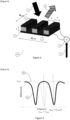
- FIG 2 schematically illustrates the resonance modes in the case of non-dispersive operation. It represents the reflectivity of the device of the figure 1 depending on the frequency and angle of the incident laser radiation (when the intermediate semiconductor layer does not absorb the incident laser radiation).
- the two horizontal bands 20 and 21 correspond to the two resonance modes TM 00 and TM 02 respectively.
- Each resonance mode has a certain line width ⁇ E.
- the frequency of the cavity resonance modes is independent of the angle of incidence of the laser radiation.
- the semiconductor layer is composed of stacks of GaAs quantum wells, having a refractive index n ⁇ 3.3.
- the linewidth of the resonance mode is ⁇ E cav .
- the separation a between the metal strips is chosen by simulation so as to be as close as possible to the optical critical coupling.
- the resonator losses (giving the linewidth of the resonance modes) are equal to the coupling rate of the photons coming from the incident radiation, which implies that all the energy of the incident radiation is absorbed.
- a fixed density of metal strips we optimize a with s fixed so as to obtain the best contrast in reflectivity as a function of the wavelength of the incident radiation.
- the device 10 can operate in dispersive mode.
- the thickness of the semiconductor layer L is chosen approximately equal to ⁇ i /10. Indeed, for such a thickness, the electromagnetic field is no longer localized only below the metal strips of the upper layer in the unit cavities which couple giving rise to the dispersive behavior.
- the micro-resonator operates in dispersive regime if the thickness L of the active region is greater than or equal to ⁇ i /10. In this operating regime, the frequency of the optical modes depends on the angle of incidence.
- FIG. 3 illustrates the two optical modes of resonance of the device 10 when it operates in the dispersive regime, that is to say when the thickness L of the active region is greater than ⁇ i /10.
- Figure 3 just like the figure 2 represents the reflectivity of the device 10 as a function of the frequency of the incident radiation when the intermediate semiconductor layer does not absorb the incident laser radiation.
- the device 10 in the dispersive regime of the embodiment of the Figure 3 has an optimal operating frequency tunable depending on the angle of incidence.
- the thickness of the active region is such that the device 10 of the figure 1 operates in a non-dispersive regime.
- the device 100 has a semiconductor layer 4 only included below the metal strips (in the unit cavities). There is no semiconductor layer between the unit cavities (between the metal strips of the top metal layer).
- the active region is etched in the portions of the active region not covered by the metal. This makes it possible to create an air/semiconductor interface between the unit cavities and therefore to obtain better confinement of the electromagnetic modes in the unit cavities. We thus obtain better coupling of the incident laser radiation in the cavity.
- the thickness of the active region L is chosen so as to operate in a non-dispersive regime. The thickness of the semiconductor layer is therefore approximately equal to ⁇ i /30. It should be noted that, in the embodiment of the Figure 4 it is in practice difficult to obtain a dispersive operating regime.
- the quantum wells have an electronic doping (n-type) of 6.10 11 cm 2 , which is introduced as delta-doping into the Al 0.3 Ga 0.7 As barriers. Alternatively, the doping can be introduced into the wells.
- vs E ISB 9.5 ⁇ m with a line width ⁇ ⁇ ⁇ ⁇ 10 % , the absorption level being proportional to the doping introduced into the quantum wells.
- This absorption line resonates with the TM 00 mode of the microcavity giving rise to a strong light-matter coupling which will be detailed below.
- the device 100 comprises a semiconductor layer consisting of a stack of a plurality of pairs of coupled quantum wells.
- the coupled quantum wells are formed by a narrow undoped well called active well and a wide electronically doped well called reservoir, separated by a first thin barrier.
- Each pair of coupled quantum wells is separated by a second barrier wider than the first.
- electronic doping can be introduced into the first thin barrier separating the wide well from the active well.
- the coupled wells are separated from each other by an 18 nm barrier of Al 0.3 Ga 0.7 As.
- the semiconductor layer of the device 100 does not absorb at 9.5 ⁇ m .
- the structure of the active region of the embodiment of the Figure 4 can be identical to that used in device 10 of the figure 1 and the structure of the active region of the embodiment of the figure 1 can be identical to that used in the device 100 of the Figure 4 .
- the semiconductor microcavity makes it possible to selectively couple a single mode of the electromagnetic field of the cavity to a single ISB plasmon mode.
- the TM 00 mode which is coupled to the ISB transition at 9.5 ⁇ m .
- the matrix element of this light-matter coupling is expressed by the quantity ⁇ rabi , called Rabi frequency. The higher this quantity ⁇ rabi , the stronger the coupling.
- L Qw the total length of the wells of the only active quantum wells in the structure
- L the total length of the semiconductor layer
- L QW the length of the active quantum wells
- f 12 the oscillator strength of the ISB transition active quantum wells (determined by numerical calculation)
- ⁇ 0 is the dielectric constant of the vacuum
- ⁇ slab is the dielectric constant of the active region
- m * is the effective mass of the electron in active quantum wells.
- n d is the electronic surface doping introduced into each quantum well, or barrier in the case of delta doping.
- n d corresponds to the doping introduced into the barriers of Al 0.3 Ga 0.7 As
- n d corresponds to the doping introduced into the reservoir wells or into the barriers.
- L QW,tot L.
- the eigenstates of the system are the mixed photon-plasmon ISB states called polaritons ( upper polaritons and lower polaritons ) .
- polaritons upper polaritons and lower polaritons
- Rabi oscillations are revealed by a separation in energy 2.
- ⁇ rabi called Rabi splitting
- a weak coupling regime between an ISB transition and a cavity resonance mode only results in a broadening of the cavity resonance.
- the quantum wells and the microcavity are parameterized so as to have ⁇ E cav , ⁇ E ISB ⁇ E ISB /10.
- the device 10 of the figure 1 absorbs incident laser radiation at frequencies ⁇ ISB ⁇ ⁇ rabi and does not absorb at frequency ⁇ ISB corresponding to the ISB transition of the quantum wells, close to a resonance mode of the cavity with frequency ⁇ cav . Indeed, the electrons are present in the quantum wells in the cavity and the strong coupling gives rise to the formation of cavity polaritons and Rabi splitting.
- the device 100 of the Figure 4 without an electric field generated between the metal layers, only laser radiation at a frequency equal to a resonance mode of the cavity ⁇ cav is absorbed by the device 100 of the Figure 4 . Indeed, the electrons coming from the doping are present in the reservoir wells and not in the active quantum wells presenting an ISB transition at the frequency ⁇ ISB close to a resonance mode of the cavity ⁇ cav .
- the semiconductor layer is therefore transparent to incident laser radiation at the frequency ⁇ cav , however the cavity allows coupling (therefore absorption) of incident laser radiation at such a frequency. Conversely, incident radiation having a frequency different from a resonance mode of the microcavity will be reflected by the device 100.
- the electrical circuit 5 is adapted to apply a voltage difference between the two metal layers.
- V 1 6 V.
- E ISB ⁇ ⁇ ⁇ Rabi ⁇ ISB ⁇ ⁇ ⁇ rabi the electrons no longer being present in the quantum wells, a photon in a resonance mode of the cavity no longer couples in strong regime, in a selective manner, to an ISB transition of the quantum wells of the semiconductor layer, creating polaritons of the cavity.
- FIG. 5 schematically illustrates the reflectivity of the device 10 as a function of the frequency of the incident laser radiation and as a function of the voltage difference applied between the metal layers.
- V 1 F * L between the two metal layers.
- Curve 51 represents the reflectivity of the device for the reflective state (a zero voltage difference between the two metal layers).
- doping is present in the quantum wells in the cavity, which gives rise to the formation of cavity polaritons and Rabi splitting at frequencies ⁇ ISB ⁇ ⁇ R from the simple ISB transition to ⁇ ISB close to a cavity resonance mode at ⁇ cav .
- This splitting causes the device 10 to absorb incident laser radiation at energies E ISB ⁇ ⁇ ⁇ Rabi ⁇ ISB ⁇ ⁇ ⁇ R and a reflection of incident laser radiation at the wavelength ⁇ ISB .
- the distance between the two metal layers L (therefore here the maximum thickness of the semiconductor layer) is not limited solely by the desire to operate in a non-dispersive cavity regime.
- the thickness of the semiconductor layer is also limited by the maximum gate voltage V max that the Schottky contacts between the semiconductor layer and the metal layers can withstand.
- insulating layers SiN, SiO2, Al2O3, etc.
- the movement of charges caused by the application of a voltage difference is a rapid phenomenon, however limited by the travel time over tens or even hundreds of nanometers of electrons from the quantum wells towards one of the metallic layers.
- the response frequency of the device 10 remains less than GHz. In order to improve the response time of this embodiment, it is possible to reduce the thickness of the semiconductor layer.
- the electrical circuit 5 is configured to apply a voltage difference chosen to create a bias or electric field making it possible to carry out a transfer by tunnel effect of the electrons introduced during doping in the reservoir wells towards the active wells. .
- This charge transfer implies that electronic doping is present in the active quantum wells in the cavity, which gives rise to the formation of cavity polaritons and Rabi splitting, with the structure then operating in strong coupling.
- the device 100 of the Figure 4 absorbs incident laser radiation at frequencies ⁇ ISB ⁇ ⁇ R and does not absorb at frequency ⁇ ISB corresponding to the ISB transition of the active quantum wells, close to a resonance mode of the cavity with frequency ⁇ cav .
- the device 100 of the Figure 4 absorbs incident laser radiation at frequencies ⁇ ISB ⁇ ⁇ R and does not absorb at frequency ⁇ ISB corresponding to the ISB transition of the active quantum wells, close to a resonance mode of the cavity with frequency ⁇ cav .
- FIG. 5 also makes it possible to schematically illustrate the reflectivity of the device 100 as a function of the frequency of the incident laser radiation and as a function of the voltage difference applied between the metal layers.
- Curve 50 represents the reflectivity of the device for the absorbing state (a zero voltage difference between the two metal layers).
- the electrons are in the reservoirs, it there is therefore no Rabi splitting and the device behaves like a “classic” microcavity: that is to say it absorbs incident laser radiation if its wavelength is equal to a resonance mode of the cavity.
- Curve 51 represents the reflectivity of the device for the reflective state (a voltage difference V 1 ⁇ 0 between the two metal layers).
- the doping is transferred from the reservoirs to the active wells, in the cavity, which gives rise to the formation of cavity polaritons and the splitting of Rabi at frequencies ⁇ ISB ⁇ ⁇ R from the simple ISB transition from active wells to ⁇ ISB close to a cavity resonance mode at ⁇ cav .
- This splitting causes the device 100 to absorb incident laser radiation at energies E ISB ⁇ ⁇ ⁇ Rabi and a reflection of incident laser radiation at the wavelength ⁇ ISB .
- the barrier between the active wells and the reservoirs being very thin (a few nanometers), the transfer by tunneling is very fast (of the order of a picosecond). Also, the response frequency of the device of the Figure 3 is very high (greater than GHz) and only limited by the RC constant of the electrical circuit.
- Another advantage of the embodiment of the Figure 3 is that the voltage difference necessary to cause the transfer of charges from the reservoirs to the active wells and therefore go from the absorbing state to the reflective state is lower than for the embodiment of the figure 1 .
- the total width d x-tot and the total length d y-tot of the device 100 are preferably much less than 200 ⁇ m. This makes it possible to reduce the RC constant of the device. We calls characteristic dimension the greatest distance between total width d x-tot and total length d y-tot.
- the contacts and microsolders are adapted so as not to limit the response time of the device.
- the device can be cooled to 78K using a cryostat or with a Peltier for example. This cooling is particularly necessary if one wishes to modulate THz waves.
- THz we define THz as ⁇ > 30 ⁇ m.
- the quantum wells are made of GaAs/AIGaAs; InGaAs/AllnAs; InAs/AISb, Si/SiGe, GaN/AIGaN or any other material making it possible to produce quantum wells with an ISB transition between 3 ⁇ m and 200 ⁇ m.
- FIG. 6 presents another embodiment of a device 1000 for modulating the amplitude of incident laser radiation. Unlike other embodiments of the invention, this device operates in transmission.
- the lower metal layer 3 has discontinuities and is structured in the same way as the upper metal layer 2 so that the metal strips of the upper and lower metal layers are opposite each other.
- the assembly formed by the two metallic layers and the intermediate semiconductor layer constitutes a micro-resonator which transmits incident radiation at a wavelength ⁇ i when the semiconductor layer 3 does not absorb for this wavelength and when ⁇ i does not correspond to a resonance mode of the cavity.
- the device comprises a substrate 8 below the lower metal layer and in contact with the latter which is a component transparent to incident laser radiation.
- This substrate can be made of CaF 2 , ZnSe, BaF 2 or any other material transparent to mid-IR radiation. Fluorine-based materials (CaF 2 , BaF 2 ) are particularly suitable because they have a low refractive index (n ⁇ 1.5) in the mid-IR spectral range.
- the substrate 8 is glued to said lower metal layer 3.
- the operating principle remains identical to the other embodiments, that is to say that thanks to the application of a voltage difference between the two metal layers using an electrical circuit 5, we go from an “absorbing state” to a “transmission state” (or the opposite depending on the structure of the active region) by causing a movement of the charges introduced by doping in the active region.
- the semiconductor layer 4 can only be included below the metal strips, there is then no semiconductor layer in the portions of the active region not covered by the metal. It is possible to remove the desired portions of semiconductor layer using an etching step for example. It should be noted that in this embodiment it is practically difficult to operate in dispersive mode.
- the upper metallic layer 2 is structured in the two directions x and y so as to form 2D resonators (or cavities) R which can be electrically connected.
- the device operates in non-dispersive regime (L ⁇ /30).
- the structuring of the layer is adapted so as to form, with the metallic layer 3 and the semiconductor layer 4, square-shaped resonators, rectangular, triangular, other... all identical and supporting resonant modes at the wavelength ⁇ i ,.
- the resonance wavelength of these resonators depends on the structuring of layer 2 and more precisely on the shape and size of the cavities. These resonance modes can be determined numerically or - for simple geometries - analytically.
- the spacing px and py in the x and y directions between the resonators is preferably chosen so as to be placed as close as possible to the critical optical coupling in order to maximize the contrast of the modulator.
- each resonator is electrically connected to an adjacent resonator in the x direction by metallic connections C of width much less than the dimensions of the resonator, to reduce the disturbance on the electromagnetic modes. More precisely, the connections are of width between 1/5 and 1/20 of the characteristic dimension of the cavity (diagonal for a rectangular cavity, side for a square cavity and diameter for a circular cavity).
- each resonator is connected to an adjacent resonator by connections in the x direction and/or in the y direction.
- Active region 4 may or may not be etched in the regions not covered by layer 2.
- This embodiment allows a reduction in the RC constant of the device by reducing the surface area of the metal layer 2 and therefore allows an increase in the modulation speed.
- the upper metal layer 2 is structured so as to allow operation of the modulation device over a widened spectral band.
- the device operates in non-dispersive regime (L ⁇ /30).
- the upper layer 2 is structured so as to consist of a plurality of identical subassemblies SE comprising a plurality of metal strips of width s i , different from the other strips of the subassembly. Each strip is separated from an adjacent strip by a distance a i in the x direction.
- the subset is repeated with periodicity Px in the direction x.
- each subset includes 3 bands.
- each subset comprises at least two bands.
- Each metal strip of width s i of the subset forms a semiconductor cavity with layer 4 and layer 3 with which is associated an absorption with or without bias centered at frequencies ( ⁇ si and ⁇ si + ⁇ rabi /2) different from those associated with other bands.
- the width of the expanded spectral band ⁇ is approximately
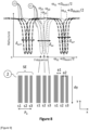
- This embodiment allows wideband operation of the modulation device because it is absorbent over a wide range of frequencies ⁇ for a zero voltage difference and over a wide range of frequencies ⁇ " and ⁇ ' for a positive voltage difference.
- the upper metallic layer 2 is structured in both x and y directions, in a manner similar to the embodiment illustrated in figure 8 , thus forming 2D resonators (cavity patch ).
- each patch cavity absorbs at a different frequency ⁇ patch_i , which depends on its shape and dimension, which is therefore different from the other patch cavity. The result is - as in the embodiment illustrated in the figure 8 in which the structuring is carried out only in the direction y- the operation of the modulator over a wider frequency range.
- the semiconductor layer 4 comprises a stack of a plurality of quantum wells with a different thickness L QW,i of quantum wells for each period i, thus constituting a stack of N tot periods.
- L QW 1 , L QW ,2 and L QW ,3 there are 3 different thicknesses of quantum wells L QW 1 , L QW ,2 and L QW ,3 .
- N 1 + N 2 + N 3 N tot periods, where N i is the number of periods of stacking of quantum wells of each of the i periods which give rise to an intersubband absorption at the frequency ⁇ ISB,i , different for each period i.
- the doping in the quantum wells will have to be multiplied by 3 to obtain an absorption at the Rabi frequency ⁇ Rabi equal to that which would have been obtained with a stack of quantum wells of a single thickness.
- a different number of three different thicknesses could be used.
- only one quantum well is used for each period.
- the quantum wells of each period are coupled wells, as in the embodiment of the Figure 4 .
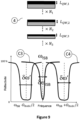
- the reflectivity of the device (curve C3) is maximum at the frequency of the cavity ⁇ cav associated with the absorption of the semiconductor cavity alone.
- the spectral width of the absorption ⁇ ISB is here only linked to the line width of the resonance mode ⁇ E cav .
- the reflectivity of the device (curve C4) of the device is maximum over two widened ranges of width ⁇ ', at approximately ⁇ cav ⁇ Rabi , because of the plurality of intersubband absorption frequency ⁇ ISB,i , associated with each period i.
Landscapes
- Physics & Mathematics (AREA)
- Nonlinear Science (AREA)
- General Physics & Mathematics (AREA)
- Optics & Photonics (AREA)
- Optical Modulation, Optical Deflection, Nonlinear Optics, Optical Demodulation, Optical Logic Elements (AREA)
- Semiconductor Lasers (AREA)
Claims (18)
- Vorrichtung (10, 100) zur Amplitudenmodulation von Laserstrahlung (1), die auf die Vorrichtung auftrifft und eine Wellenlänge λi aufweist, dadurch gekennzeichnet, dass sie umfasst: eine untere Metallschicht (3), über der sich eine Halbleiterschicht (4) befindet, die eine Schichtung aus einer Vielzahl von Quantentöpfen enthält, über der sich eine strukturierte obere Metallschicht (2) befindet, wobei beide Metallschichten (2, 3) für die einfallende Laserstrahlung (1) reflektierend sind, wobei die Strukturierung der oberen Schicht und der Abstand zwischen den beiden Metallschichten L ausreichend klein ist, damit die Vorrichtung einen optischen Mikrohohlraum bildet, der mindestens einen Resonanzmodus aufweist;wobei mindestens ein Teil der sogenannten aktiven Quantenschächte eine Intersubbandabsorption bei einer zentralen Wellenlänge λ/SB = hc/EISB aufweist, wobei die Kopplung zwischen dem Intersubbandübergang bei der zentralen Wellenlänge λ/SB und einen der Modi des Mikrohohlraums die Anregung von Hohlraumpolaritonen und eine Rabi-Spaltung bei den Energien
 wobei die Vorrichtung eine elektrische Schaltung (5) umfasst, die so konfiguriert ist, dass sie zwei verschiedene Spannungsdifferenzen, V0 und V1, zwischen den beiden Metallschichten anlegt, wobei die Vorrichtung (4) die einfallende Strahlung (1) für die Spannungsdifferenz V0 absorbiert und die Vorrichtung die einfallende Strahlung für die Spannungsdifferenz V1 reflektiert oder überträgt.
 - Vorrichtung nach dem vorhergehenden Anspruch, in der die untere Metallschicht keine Unterbrechungen aufweist und die Vorrichtung die einfallende Strahlung für die Spannungsdifferenz V1 reflektiert.
- Vorrichtung nach einem der vorhergehenden Ansprüche, in der die obere Metallschicht aus einer Vielzahl von Metallstreifen mit einer Breite s gebildet wird, die durch einen Abstand α getrennt sind, wobei s + α < λi /2 gilt.
- Vorrichtung nach dem vorhergehenden Anspruch, in der die Breite der Metallstreifen s so ist, dass s = λi / 2.n bei ±30% mit n dem Index der Halbleiterschicht.
- Vorrichtung nach Anspruch 3, in der die Breite der Metallstreifen s = λi /2.ns so ist, dass s = 3.λi /2.ns bei ±30%, mit n dem Index der Halbleiterschicht.
- Vorrichtung nach einem der vorhergehenden Ansprüche, in der die Kontakte zwischen der Halbleiterschicht und den Metallschichten durch Schottky-Kontakte oder durch das Einbringen von Isolierschichten hergestellt werden.
- Vorrichtung nach dem vorhergehenden Anspruch, in der der Abstand zwischen den beiden Metallschichten L gleich λi /30 bei ± 30% ist.
- Vorrichtung nach dem vorhergehenden Anspruch, in der der Abstand zwischen den beiden Metallschichten L durch numerische Simulationen so gewählt wird, dass die Vorrichtung in einem nicht-dispersiven Regime arbeitet.
- Vorrichtung (10) nach dem vorhergehenden Anspruch, in der die Quantentöpfe oder die Barrieren, die die Quantentöpfe trennen, elektronisch dotiert sind, wobei die Quantentöpfe so gewählt sind, dass für eine erste Spannungsdifferenz V0 , die von der elektrischen Schaltung (5) zwischen den beiden Metallschichten angelegt wird, die Vorrichtung eine Absorption bei den Energien


- Vorrichtung nach dem vorhergehenden Anspruch, in der die Dicke der Halbleiterschicht L so ist, dass V1 kleiner ist als die maximale Spannung, die von den Kontakten zwischen der Halbleiterschicht und den Metallschichten vertragen wird.
- Vorrichtung nach dem vorhergehenden Anspruch, in der die Dicke L der Halbleiterschicht so gewählt ist, dass V1 kleiner als 10V ist.
- Vorrichtung nach einem der Ansprüche 1 bis 6, in der der Abstand zwischen den beiden Metallschichten L gleich λi /10 bei ± 30% ist.
- Vorrichtung (100) nach einem der Ansprüche 1 bis 7 und 8 bis 11, in der die Halbleiterschicht eine Schichtung gekoppelter Quantentöpfe umfasst, die aus einem nicht dotierten schmalen Topf, dem sogenannten aktiven Topf, besteht, der durch eine erste Barriere von einem breiten Topf, dem sogenannten Reservoir, getrennt ist, wobei die gekoppelten Quantentöpfe voneinander zudem durch eine zweite Barriere getrennt sind, die breiter ist als die erste Barriere, wobei die erste Barriere oder das Reservoir jedes gekoppelten Quantentopfes elektronisch dotiert ist und die aktiven Töpfe so ausgewählt werden, dass sie eine Intersubbandabsorption bei einer Zentralwellenlänge λ ISB nahe eines Resonanzmodus des optischen Mikrohohlraums aufweisen; wobei die gekoppelten Quantentöpfe so ausgelegt sind, dass bei einer ersten Spannungsdifferenz V0 , die von der elektrischen Schaltung (5) zwischen den beiden Metallschichten angelegt wird, die Ladungen aus der Dotierung durch Tunneleffekt in die schmalen Töpfe übertragen werden und die Vorrichtung eine Absorption bei Energien


- Vorrichtung nach dem vorhergehenden Anspruch, in der die Dicke L der Halbleiterschicht so gewählt ist, dass V0 kleiner gleich 2V ist.
- Vorrichtung nach einem der Ansprüche 2 bis 12, in der die Halbleiterschicht so strukturiert ist, dass die Quantentopfschichtungen nur direkt unter den Metallstreifen der oberen Metallschicht liegen.
- Vorrichtung nach einem der vorhergehenden Ansprüche, in der die Quantentöpfe der Halbleiterschicht aus GaAs/AIGaAs; InGaAs/AlInAs; InAs/AISb, Si/SiGe, GaN/AlGaN hergestellt sind.
- Vorrichtung nach einem der vorhergehenden Ansprüche, in der eine charakteristische Größe der Vorrichtung weniger als 200 µm beträgt.
- Vorrichtung nach einem der Ansprüche 3 bis 17, in der die untere Metallschicht Diskontinuitäten aufweist und so strukturiert ist, dass die Vorrichtung die einfallende Strahlung für die Spannungsdifferenz V1 überträgt, wobei die Vorrichtung ein Substrat 8 umfasst, das unterhalb der unteren Metallschicht und in Kontakt mit dieser für die einfallende Strahlung transparent ist.
Applications Claiming Priority (2)
| Application Number | Priority Date | Filing Date | Title |
|---|---|---|---|
| FR1903211A FR3094503A1 (fr) | 2019-03-27 | 2019-03-27 | Modulateur ultra-rapide de l’amplitude d’un rayonnement laser |
| PCT/EP2020/058841 WO2020193786A1 (fr) | 2019-03-27 | 2020-03-27 | Modulateur ultra-rapide de l'amplitude d'un rayonnement laser |
Publications (2)
| Publication Number | Publication Date |
|---|---|
| EP3948409A1 EP3948409A1 (de) | 2022-02-09 |
| EP3948409B1 true EP3948409B1 (de) | 2024-03-13 |
Family
ID=68654530
Family Applications (1)
| Application Number | Title | Priority Date | Filing Date |
|---|---|---|---|
| EP20713320.8A Active EP3948409B1 (de) | 2019-03-27 | 2020-03-27 | Ultraschneller modulator zur modulation der amplitude von laserstrahlung |
Country Status (5)
| Country | Link |
|---|---|
| US (1) | US12055801B2 (de) |
| EP (1) | EP3948409B1 (de) |
| JP (1) | JP7729777B2 (de) |
| FR (1) | FR3094503A1 (de) |
| WO (1) | WO2020193786A1 (de) |
Families Citing this family (1)
| Publication number | Priority date | Publication date | Assignee | Title |
|---|---|---|---|---|
| FR3162867B1 (fr) | 2024-06-03 | 2026-04-24 | Univ Limoges | Système de microscopie par fluorescence, Système de diagnostic par laser et Procédé d’imagerie par fluorescence |
Family Cites Families (8)
| Publication number | Priority date | Publication date | Assignee | Title |
|---|---|---|---|---|
| JP2757996B2 (ja) * | 1988-06-17 | 1998-05-25 | 日本放送協会 | 空間光変調素子 |
| FR2741483B1 (fr) * | 1995-11-21 | 1998-01-02 | Thomson Csf | Dispositif optoelectronique a puits quantiques |
| EP1729383A1 (de) * | 2005-05-30 | 2006-12-06 | Ecole Polytechnique Federale De Lausanne | Einzelphotonenquelle |
| FR2886745B1 (fr) * | 2005-06-06 | 2007-10-12 | Centre Nat Rech Scient | Micro-oscillateur parametrique optique a cavites |
| US9748736B1 (en) * | 2012-10-16 | 2017-08-29 | The Regents Of The University Of California | Waveguide embedded plasmon laser with multiplexing and electrical modulation |
| EP3113304B1 (de) * | 2014-02-28 | 2022-04-13 | Japan Science and Technology Agency | Wärmestrahlungslichtquelle und darin verwendeter zweidimensionaler photonischer kristall |
| US10353269B2 (en) * | 2016-02-26 | 2019-07-16 | The Trustees Of Princeton University | Multi-mode cavities for high-efficiency nonlinear wavelength conversion formed with overlap optimization |
| US20180196138A1 (en) * | 2017-01-10 | 2018-07-12 | Samsung Electronics Co., Ltd. | Optical modulating device and system including the same |
-
2019
- 2019-03-27 FR FR1903211A patent/FR3094503A1/fr active Pending
-
2020
- 2020-03-27 JP JP2021557521A patent/JP7729777B2/ja active Active
- 2020-03-27 EP EP20713320.8A patent/EP3948409B1/de active Active
- 2020-03-27 WO PCT/EP2020/058841 patent/WO2020193786A1/fr not_active Ceased
- 2020-03-27 US US17/598,632 patent/US12055801B2/en active Active
Also Published As
| Publication number | Publication date |
|---|---|
| US20220187634A1 (en) | 2022-06-16 |
| WO2020193786A1 (fr) | 2020-10-01 |
| EP3948409A1 (de) | 2022-02-09 |
| JP7729777B2 (ja) | 2025-08-26 |
| US12055801B2 (en) | 2024-08-06 |
| FR3094503A1 (fr) | 2020-10-02 |
| JP2022526357A (ja) | 2022-05-24 |
| WO2020193786A9 (fr) | 2020-11-19 |
Similar Documents
| Publication | Publication Date | Title |
|---|---|---|
| EP2676166B1 (de) | Terahertzmodulator | |
| EP0575227B1 (de) | Verfahren und Vorrichtung zur Modulation und Verstärkung von Lichtstrahlen | |
| EP2289134B1 (de) | Lasergerät mit terahertzwellenemission | |
| EP0762577B1 (de) | Halbleitende Emissionsvorrichtung mit schneller Wellenlängenmodulation | |
| EP0531214B1 (de) | Monolithisch integrierte Laserdioden-Modulator mit einem stark gekoppelten Übergitter | |
| EP2660938B1 (de) | Laservorrichtung mit gelochter Struktur, die Terahertz-Wellen ausstrahlt | |
| EP0306400B1 (de) | Quantum-well-Modulator für elektromagnetische Wellen und Anwendung dieses Modulators als Polarisator | |
| Barron et al. | Millimeter-wave asymmetric Fabry-Perot modulators | |
| EP0436413B1 (de) | Verfahren und Vorrichtung zur elektrooptischen Modulation unter Benutzung des niederenergetischen schrägen Überganges in einem stark gekoppelten Übergitter | |
| WO2020193786A9 (fr) | Modulateur ultra-rapide de l'amplitude d'un rayonnement laser | |
| EP0274289B1 (de) | Optischer Übergitter-Modulator | |
| EP0736791B1 (de) | Photorefraktives Quantentopfbauelement | |
| Biyikli et al. | High-Speed visible-blind resonant cavity enhanced AlGaN Schottky photodiodes | |
| EP0477072B1 (de) | Mehrschichtiger elektrooptischer Lichtmodulator | |
| EP1896896A1 (de) | Optischer parametrischer mikrooszillator mit gekoppelten resonatoren | |
| EP0640866B1 (de) | Reine optische bistabile Vorrichtung vom "SEED"-Typ | |
| EP0545787B1 (de) | Halbleiterheterostruktur für die Verarbeitung eines optischen Signals | |
| EP0805371A1 (de) | Elektrooptischer Modulator mit Quantentöpfen | |
| Qasaimeh | Bistability characteristics of different types of optical modes amplified by quantum dot vertical cavity semiconductor optical amplifiers | |
| EP2194422B1 (de) | Modulator eines optischen Trägers durch Oberflächenplasmonen auf der Basis von Halbleitermaterialien | |
| EP4375880A1 (de) | Gepulste laservorrichtung mit aktiver optischer trigger-hybridlaserquelle | |
| JP2004226531A (ja) | 電磁波強度変調器 | |
| Dogariu et al. | Real-time detection of bacterial spores | |
| WO2004017477A1 (fr) | Laser largement accordable sur cristal photonique | |
| FR2817630A1 (fr) | Dispositif d'emission d'onde lumineuse dans la gamme du teraherz |
Legal Events
| Date | Code | Title | Description |
|---|---|---|---|
| STAA | Information on the status of an ep patent application or granted ep patent |
Free format text: STATUS: UNKNOWN |
|
| STAA | Information on the status of an ep patent application or granted ep patent |
Free format text: STATUS: THE INTERNATIONAL PUBLICATION HAS BEEN MADE |
|
| PUAI | Public reference made under article 153(3) epc to a published international application that has entered the european phase |
Free format text: ORIGINAL CODE: 0009012 |
|
| STAA | Information on the status of an ep patent application or granted ep patent |
Free format text: STATUS: REQUEST FOR EXAMINATION WAS MADE |
|
| 17P | Request for examination filed |
Effective date: 20210930 |
|
| AK | Designated contracting states |
Kind code of ref document: A1 Designated state(s): AL AT BE BG CH CY CZ DE DK EE ES FI FR GB GR HR HU IE IS IT LI LT LU LV MC MK MT NL NO PL PT RO RS SE SI SK SM TR |
|
| DAV | Request for validation of the european patent (deleted) | ||
| DAX | Request for extension of the european patent (deleted) | ||
| GRAP | Despatch of communication of intention to grant a patent |
Free format text: ORIGINAL CODE: EPIDOSNIGR1 |
|
| STAA | Information on the status of an ep patent application or granted ep patent |
Free format text: STATUS: GRANT OF PATENT IS INTENDED |
|
| INTG | Intention to grant announced |
Effective date: 20231017 |
|
| GRAS | Grant fee paid |
Free format text: ORIGINAL CODE: EPIDOSNIGR3 |
|
| GRAA | (expected) grant |
Free format text: ORIGINAL CODE: 0009210 |
|
| STAA | Information on the status of an ep patent application or granted ep patent |
Free format text: STATUS: THE PATENT HAS BEEN GRANTED |
|
| RAP1 | Party data changed (applicant data changed or rights of an application transferred) |
Owner name: UNIVERSITE PARIS-SACLAY Owner name: CENTRE NATIONAL DE LA RECHERCHE SCIENTIFIQUE |
|
| AK | Designated contracting states |
Kind code of ref document: B1 Designated state(s): AL AT BE BG CH CY CZ DE DK EE ES FI FR GB GR HR HU IE IS IT LI LT LU LV MC MK MT NL NO PL PT RO RS SE SI SK SM TR |
|
| REG | Reference to a national code |
Ref country code: GB Ref legal event code: FG4D Free format text: NOT ENGLISH |
|
| REG | Reference to a national code |
Ref country code: CH Ref legal event code: EP |
|
| REG | Reference to a national code |
Ref country code: DE Ref legal event code: R096 Ref document number: 602020027158 Country of ref document: DE |
|
| REG | Reference to a national code |
Ref country code: IE Ref legal event code: FG4D Free format text: LANGUAGE OF EP DOCUMENT: FRENCH |
|
| PG25 | Lapsed in a contracting state [announced via postgrant information from national office to epo] |
Ref country code: LT Free format text: LAPSE BECAUSE OF FAILURE TO SUBMIT A TRANSLATION OF THE DESCRIPTION OR TO PAY THE FEE WITHIN THE PRESCRIBED TIME-LIMIT Effective date: 20240313 |
|
| REG | Reference to a national code |
Ref country code: LT Ref legal event code: MG9D |
|
| PG25 | Lapsed in a contracting state [announced via postgrant information from national office to epo] |
Ref country code: GR Free format text: LAPSE BECAUSE OF FAILURE TO SUBMIT A TRANSLATION OF THE DESCRIPTION OR TO PAY THE FEE WITHIN THE PRESCRIBED TIME-LIMIT Effective date: 20240614 |
|
| REG | Reference to a national code |
Ref country code: NL Ref legal event code: MP Effective date: 20240313 |
|
| PG25 | Lapsed in a contracting state [announced via postgrant information from national office to epo] |
Ref country code: RS Free format text: LAPSE BECAUSE OF FAILURE TO SUBMIT A TRANSLATION OF THE DESCRIPTION OR TO PAY THE FEE WITHIN THE PRESCRIBED TIME-LIMIT Effective date: 20240613 Ref country code: HR Free format text: LAPSE BECAUSE OF FAILURE TO SUBMIT A TRANSLATION OF THE DESCRIPTION OR TO PAY THE FEE WITHIN THE PRESCRIBED TIME-LIMIT Effective date: 20240313 |
|
| PG25 | Lapsed in a contracting state [announced via postgrant information from national office to epo] |
Ref country code: ES Free format text: LAPSE BECAUSE OF FAILURE TO SUBMIT A TRANSLATION OF THE DESCRIPTION OR TO PAY THE FEE WITHIN THE PRESCRIBED TIME-LIMIT Effective date: 20240313 |
|
| PG25 | Lapsed in a contracting state [announced via postgrant information from national office to epo] |
Ref country code: RS Free format text: LAPSE BECAUSE OF FAILURE TO SUBMIT A TRANSLATION OF THE DESCRIPTION OR TO PAY THE FEE WITHIN THE PRESCRIBED TIME-LIMIT Effective date: 20240613 Ref country code: NO Free format text: LAPSE BECAUSE OF FAILURE TO SUBMIT A TRANSLATION OF THE DESCRIPTION OR TO PAY THE FEE WITHIN THE PRESCRIBED TIME-LIMIT Effective date: 20240613 Ref country code: LT Free format text: LAPSE BECAUSE OF FAILURE TO SUBMIT A TRANSLATION OF THE DESCRIPTION OR TO PAY THE FEE WITHIN THE PRESCRIBED TIME-LIMIT Effective date: 20240313 Ref country code: HR Free format text: LAPSE BECAUSE OF FAILURE TO SUBMIT A TRANSLATION OF THE DESCRIPTION OR TO PAY THE FEE WITHIN THE PRESCRIBED TIME-LIMIT Effective date: 20240313 Ref country code: GR Free format text: LAPSE BECAUSE OF FAILURE TO SUBMIT A TRANSLATION OF THE DESCRIPTION OR TO PAY THE FEE WITHIN THE PRESCRIBED TIME-LIMIT Effective date: 20240614 Ref country code: FI Free format text: LAPSE BECAUSE OF FAILURE TO SUBMIT A TRANSLATION OF THE DESCRIPTION OR TO PAY THE FEE WITHIN THE PRESCRIBED TIME-LIMIT Effective date: 20240313 Ref country code: ES Free format text: LAPSE BECAUSE OF FAILURE TO SUBMIT A TRANSLATION OF THE DESCRIPTION OR TO PAY THE FEE WITHIN THE PRESCRIBED TIME-LIMIT Effective date: 20240313 Ref country code: BG Free format text: LAPSE BECAUSE OF FAILURE TO SUBMIT A TRANSLATION OF THE DESCRIPTION OR TO PAY THE FEE WITHIN THE PRESCRIBED TIME-LIMIT Effective date: 20240313 |
|
| REG | Reference to a national code |
Ref country code: AT Ref legal event code: MK05 Ref document number: 1666301 Country of ref document: AT Kind code of ref document: T Effective date: 20240313 |
|
| PG25 | Lapsed in a contracting state [announced via postgrant information from national office to epo] |
Ref country code: SE Free format text: LAPSE BECAUSE OF FAILURE TO SUBMIT A TRANSLATION OF THE DESCRIPTION OR TO PAY THE FEE WITHIN THE PRESCRIBED TIME-LIMIT Effective date: 20240313 Ref country code: LV Free format text: LAPSE BECAUSE OF FAILURE TO SUBMIT A TRANSLATION OF THE DESCRIPTION OR TO PAY THE FEE WITHIN THE PRESCRIBED TIME-LIMIT Effective date: 20240313 |
|
| PG25 | Lapsed in a contracting state [announced via postgrant information from national office to epo] |
Ref country code: NL Free format text: LAPSE BECAUSE OF FAILURE TO SUBMIT A TRANSLATION OF THE DESCRIPTION OR TO PAY THE FEE WITHIN THE PRESCRIBED TIME-LIMIT Effective date: 20240313 |
|
| PG25 | Lapsed in a contracting state [announced via postgrant information from national office to epo] |
Ref country code: NL Free format text: LAPSE BECAUSE OF FAILURE TO SUBMIT A TRANSLATION OF THE DESCRIPTION OR TO PAY THE FEE WITHIN THE PRESCRIBED TIME-LIMIT Effective date: 20240313 |
|
| PG25 | Lapsed in a contracting state [announced via postgrant information from national office to epo] |
Ref country code: IS Free format text: LAPSE BECAUSE OF FAILURE TO SUBMIT A TRANSLATION OF THE DESCRIPTION OR TO PAY THE FEE WITHIN THE PRESCRIBED TIME-LIMIT Effective date: 20240713 |
|
| PG25 | Lapsed in a contracting state [announced via postgrant information from national office to epo] |
Ref country code: SM Free format text: LAPSE BECAUSE OF FAILURE TO SUBMIT A TRANSLATION OF THE DESCRIPTION OR TO PAY THE FEE WITHIN THE PRESCRIBED TIME-LIMIT Effective date: 20240313 Ref country code: PT Free format text: LAPSE BECAUSE OF FAILURE TO SUBMIT A TRANSLATION OF THE DESCRIPTION OR TO PAY THE FEE WITHIN THE PRESCRIBED TIME-LIMIT Effective date: 20240715 |
|
| PG25 | Lapsed in a contracting state [announced via postgrant information from national office to epo] |
Ref country code: CZ Free format text: LAPSE BECAUSE OF FAILURE TO SUBMIT A TRANSLATION OF THE DESCRIPTION OR TO PAY THE FEE WITHIN THE PRESCRIBED TIME-LIMIT Effective date: 20240313 Ref country code: EE Free format text: LAPSE BECAUSE OF FAILURE TO SUBMIT A TRANSLATION OF THE DESCRIPTION OR TO PAY THE FEE WITHIN THE PRESCRIBED TIME-LIMIT Effective date: 20240313 |
|
| PG25 | Lapsed in a contracting state [announced via postgrant information from national office to epo] |
Ref country code: AT Free format text: LAPSE BECAUSE OF FAILURE TO SUBMIT A TRANSLATION OF THE DESCRIPTION OR TO PAY THE FEE WITHIN THE PRESCRIBED TIME-LIMIT Effective date: 20240313 |
|
| PG25 | Lapsed in a contracting state [announced via postgrant information from national office to epo] |
Ref country code: PL Free format text: LAPSE BECAUSE OF FAILURE TO SUBMIT A TRANSLATION OF THE DESCRIPTION OR TO PAY THE FEE WITHIN THE PRESCRIBED TIME-LIMIT Effective date: 20240313 |
|
| PG25 | Lapsed in a contracting state [announced via postgrant information from national office to epo] |
Ref country code: SK Free format text: LAPSE BECAUSE OF FAILURE TO SUBMIT A TRANSLATION OF THE DESCRIPTION OR TO PAY THE FEE WITHIN THE PRESCRIBED TIME-LIMIT Effective date: 20240313 |
|
| PG25 | Lapsed in a contracting state [announced via postgrant information from national office to epo] |
Ref country code: SM Free format text: LAPSE BECAUSE OF FAILURE TO SUBMIT A TRANSLATION OF THE DESCRIPTION OR TO PAY THE FEE WITHIN THE PRESCRIBED TIME-LIMIT Effective date: 20240313 Ref country code: SK Free format text: LAPSE BECAUSE OF FAILURE TO SUBMIT A TRANSLATION OF THE DESCRIPTION OR TO PAY THE FEE WITHIN THE PRESCRIBED TIME-LIMIT Effective date: 20240313 Ref country code: RO Free format text: LAPSE BECAUSE OF FAILURE TO SUBMIT A TRANSLATION OF THE DESCRIPTION OR TO PAY THE FEE WITHIN THE PRESCRIBED TIME-LIMIT Effective date: 20240313 Ref country code: PT Free format text: LAPSE BECAUSE OF FAILURE TO SUBMIT A TRANSLATION OF THE DESCRIPTION OR TO PAY THE FEE WITHIN THE PRESCRIBED TIME-LIMIT Effective date: 20240715 Ref country code: PL Free format text: LAPSE BECAUSE OF FAILURE TO SUBMIT A TRANSLATION OF THE DESCRIPTION OR TO PAY THE FEE WITHIN THE PRESCRIBED TIME-LIMIT Effective date: 20240313 Ref country code: IS Free format text: LAPSE BECAUSE OF FAILURE TO SUBMIT A TRANSLATION OF THE DESCRIPTION OR TO PAY THE FEE WITHIN THE PRESCRIBED TIME-LIMIT Effective date: 20240713 Ref country code: EE Free format text: LAPSE BECAUSE OF FAILURE TO SUBMIT A TRANSLATION OF THE DESCRIPTION OR TO PAY THE FEE WITHIN THE PRESCRIBED TIME-LIMIT Effective date: 20240313 Ref country code: CZ Free format text: LAPSE BECAUSE OF FAILURE TO SUBMIT A TRANSLATION OF THE DESCRIPTION OR TO PAY THE FEE WITHIN THE PRESCRIBED TIME-LIMIT Effective date: 20240313 Ref country code: AT Free format text: LAPSE BECAUSE OF FAILURE TO SUBMIT A TRANSLATION OF THE DESCRIPTION OR TO PAY THE FEE WITHIN THE PRESCRIBED TIME-LIMIT Effective date: 20240313 |
|
| REG | Reference to a national code |
Ref country code: CH Ref legal event code: PL |
|
| PG25 | Lapsed in a contracting state [announced via postgrant information from national office to epo] |
Ref country code: LU Free format text: LAPSE BECAUSE OF NON-PAYMENT OF DUE FEES Effective date: 20240327 |
|
| PG25 | Lapsed in a contracting state [announced via postgrant information from national office to epo] |
Ref country code: LU Free format text: LAPSE BECAUSE OF NON-PAYMENT OF DUE FEES Effective date: 20240327 |
|
| PG25 | Lapsed in a contracting state [announced via postgrant information from national office to epo] |
Ref country code: IT Free format text: LAPSE BECAUSE OF FAILURE TO SUBMIT A TRANSLATION OF THE DESCRIPTION OR TO PAY THE FEE WITHIN THE PRESCRIBED TIME-LIMIT Effective date: 20240313 |
|
| REG | Reference to a national code |
Ref country code: DE Ref legal event code: R097 Ref document number: 602020027158 Country of ref document: DE Ref country code: BE Ref legal event code: MM Effective date: 20240331 |
|
| PG25 | Lapsed in a contracting state [announced via postgrant information from national office to epo] |
Ref country code: IT Free format text: LAPSE BECAUSE OF FAILURE TO SUBMIT A TRANSLATION OF THE DESCRIPTION OR TO PAY THE FEE WITHIN THE PRESCRIBED TIME-LIMIT Effective date: 20240313 |
|
| PG25 | Lapsed in a contracting state [announced via postgrant information from national office to epo] |
Ref country code: MC Free format text: LAPSE BECAUSE OF FAILURE TO SUBMIT A TRANSLATION OF THE DESCRIPTION OR TO PAY THE FEE WITHIN THE PRESCRIBED TIME-LIMIT Effective date: 20240313 |
|
| PG25 | Lapsed in a contracting state [announced via postgrant information from national office to epo] |
Ref country code: DK Free format text: LAPSE BECAUSE OF FAILURE TO SUBMIT A TRANSLATION OF THE DESCRIPTION OR TO PAY THE FEE WITHIN THE PRESCRIBED TIME-LIMIT Effective date: 20240313 |
|
| PG25 | Lapsed in a contracting state [announced via postgrant information from national office to epo] |
Ref country code: BE Free format text: LAPSE BECAUSE OF NON-PAYMENT OF DUE FEES Effective date: 20240331 |
|
| PLBE | No opposition filed within time limit |
Free format text: ORIGINAL CODE: 0009261 |
|
| STAA | Information on the status of an ep patent application or granted ep patent |
Free format text: STATUS: NO OPPOSITION FILED WITHIN TIME LIMIT |
|
| PG25 | Lapsed in a contracting state [announced via postgrant information from national office to epo] |
Ref country code: IE Free format text: LAPSE BECAUSE OF NON-PAYMENT OF DUE FEES Effective date: 20240327 |
|
| PG25 | Lapsed in a contracting state [announced via postgrant information from national office to epo] |
Ref country code: MC Free format text: LAPSE BECAUSE OF FAILURE TO SUBMIT A TRANSLATION OF THE DESCRIPTION OR TO PAY THE FEE WITHIN THE PRESCRIBED TIME-LIMIT Effective date: 20240313 Ref country code: IE Free format text: LAPSE BECAUSE OF NON-PAYMENT OF DUE FEES Effective date: 20240327 Ref country code: DK Free format text: LAPSE BECAUSE OF FAILURE TO SUBMIT A TRANSLATION OF THE DESCRIPTION OR TO PAY THE FEE WITHIN THE PRESCRIBED TIME-LIMIT Effective date: 20240313 Ref country code: BE Free format text: LAPSE BECAUSE OF NON-PAYMENT OF DUE FEES Effective date: 20240331 Ref country code: CH Free format text: LAPSE BECAUSE OF NON-PAYMENT OF DUE FEES Effective date: 20240331 |
|
| 26N | No opposition filed |
Effective date: 20241216 |
|
| PG25 | Lapsed in a contracting state [announced via postgrant information from national office to epo] |
Ref country code: SI Free format text: LAPSE BECAUSE OF FAILURE TO SUBMIT A TRANSLATION OF THE DESCRIPTION OR TO PAY THE FEE WITHIN THE PRESCRIBED TIME-LIMIT Effective date: 20240313 |
|
| PGFP | Annual fee paid to national office [announced via postgrant information from national office to epo] |
Ref country code: DE Payment date: 20250425 Year of fee payment: 6 |
|
| PG25 | Lapsed in a contracting state [announced via postgrant information from national office to epo] |
Ref country code: CY Free format text: LAPSE BECAUSE OF FAILURE TO SUBMIT A TRANSLATION OF THE DESCRIPTION OR TO PAY THE FEE WITHIN THE PRESCRIBED TIME-LIMIT; INVALID AB INITIO Effective date: 20200327 |
|
| PG25 | Lapsed in a contracting state [announced via postgrant information from national office to epo] |
Ref country code: HU Free format text: LAPSE BECAUSE OF FAILURE TO SUBMIT A TRANSLATION OF THE DESCRIPTION OR TO PAY THE FEE WITHIN THE PRESCRIBED TIME-LIMIT; INVALID AB INITIO Effective date: 20200327 |
|
| PG25 | Lapsed in a contracting state [announced via postgrant information from national office to epo] |
Ref country code: TR Free format text: LAPSE BECAUSE OF FAILURE TO SUBMIT A TRANSLATION OF THE DESCRIPTION OR TO PAY THE FEE WITHIN THE PRESCRIBED TIME-LIMIT Effective date: 20240313 |
|
| PGFP | Annual fee paid to national office [announced via postgrant information from national office to epo] |
Ref country code: GB Payment date: 20260330 Year of fee payment: 7 |
|
| PGFP | Annual fee paid to national office [announced via postgrant information from national office to epo] |
Ref country code: FR Payment date: 20260330 Year of fee payment: 7 |