EP3950153A1 - Procédé de traitement de déchets de composants de dispositifs électroniques/électriques - Google Patents
Procédé de traitement de déchets de composants de dispositifs électroniques/électriques Download PDFInfo
- Publication number
- EP3950153A1 EP3950153A1 EP20781759.4A EP20781759A EP3950153A1 EP 3950153 A1 EP3950153 A1 EP 3950153A1 EP 20781759 A EP20781759 A EP 20781759A EP 3950153 A1 EP3950153 A1 EP 3950153A1
- Authority
- EP
- European Patent Office
- Prior art keywords
- metal
- electrical device
- device component
- electronic
- objects
- Prior art date
- Legal status (The legal status is an assumption and is not a legal conclusion. Google has not performed a legal analysis and makes no representation as to the accuracy of the status listed.)
- Withdrawn
Links
Images

Classifications
-
- B—PERFORMING OPERATIONS; TRANSPORTING
- B03—SEPARATION OF SOLID MATERIALS USING LIQUIDS OR USING PNEUMATIC TABLES OR JIGS; MAGNETIC OR ELECTROSTATIC SEPARATION OF SOLID MATERIALS FROM SOLID MATERIALS OR FLUIDS; SEPARATION BY HIGH-VOLTAGE ELECTRIC FIELDS
- B03B—SEPARATING SOLID MATERIALS USING LIQUIDS OR USING PNEUMATIC TABLES OR JIGS
- B03B9/00—General arrangement of separating plant, e.g. flow sheets
-
- B—PERFORMING OPERATIONS; TRANSPORTING
- B07—SEPARATING SOLIDS FROM SOLIDS; SORTING
- B07C—POSTAL SORTING; SORTING INDIVIDUAL ARTICLES, OR BULK MATERIAL FIT TO BE SORTED PIECE-MEAL, e.g. BY PICKING
- B07C5/00—Sorting according to a characteristic or feature of the articles or material being sorted, e.g. by control effected by devices which detect or measure such characteristic or feature; Sorting by manually actuated devices, e.g. switches
- B07C5/36—Sorting apparatus characterised by the means used for distribution
- B07C5/363—Sorting apparatus characterised by the means used for distribution by means of air
- B07C5/365—Sorting apparatus characterised by the means used for distribution by means of air using a single separation means
- B07C5/366—Sorting apparatus characterised by the means used for distribution by means of air using a single separation means during free fall of the articles
-
- B—PERFORMING OPERATIONS; TRANSPORTING
- B03—SEPARATION OF SOLID MATERIALS USING LIQUIDS OR USING PNEUMATIC TABLES OR JIGS; MAGNETIC OR ELECTROSTATIC SEPARATION OF SOLID MATERIALS FROM SOLID MATERIALS OR FLUIDS; SEPARATION BY HIGH-VOLTAGE ELECTRIC FIELDS
- B03B—SEPARATING SOLID MATERIALS USING LIQUIDS OR USING PNEUMATIC TABLES OR JIGS
- B03B9/00—General arrangement of separating plant, e.g. flow sheets
- B03B9/06—General arrangement of separating plant, e.g. flow sheets specially adapted for refuse
- B03B9/061—General arrangement of separating plant, e.g. flow sheets specially adapted for refuse the refuse being industrial
-
- B—PERFORMING OPERATIONS; TRANSPORTING
- B07—SEPARATING SOLIDS FROM SOLIDS; SORTING
- B07B—SEPARATING SOLIDS FROM SOLIDS BY SIEVING, SCREENING, SIFTING OR BY USING GAS CURRENTS; SEPARATING BY OTHER DRY METHODS APPLICABLE TO BULK MATERIAL, e.g. LOOSE ARTICLES FIT TO BE HANDLED LIKE BULK MATERIAL
- B07B1/00—Sieving, screening, sifting, or sorting solid materials using networks, gratings, grids, or the like
-
- B—PERFORMING OPERATIONS; TRANSPORTING
- B07—SEPARATING SOLIDS FROM SOLIDS; SORTING
- B07B—SEPARATING SOLIDS FROM SOLIDS BY SIEVING, SCREENING, SIFTING OR BY USING GAS CURRENTS; SEPARATING BY OTHER DRY METHODS APPLICABLE TO BULK MATERIAL, e.g. LOOSE ARTICLES FIT TO BE HANDLED LIKE BULK MATERIAL
- B07B7/00—Selective separation of solid materials carried by, or dispersed in, gas currents
-
- B—PERFORMING OPERATIONS; TRANSPORTING
- B07—SEPARATING SOLIDS FROM SOLIDS; SORTING
- B07C—POSTAL SORTING; SORTING INDIVIDUAL ARTICLES, OR BULK MATERIAL FIT TO BE SORTED PIECE-MEAL, e.g. BY PICKING
- B07C5/00—Sorting according to a characteristic or feature of the articles or material being sorted, e.g. by control effected by devices which detect or measure such characteristic or feature; Sorting by manually actuated devices, e.g. switches
- B07C5/34—Sorting according to other particular properties
- B07C5/342—Sorting according to other particular properties according to optical properties, e.g. colour
-
- B—PERFORMING OPERATIONS; TRANSPORTING
- B09—DISPOSAL OF SOLID WASTE; RECLAMATION OF CONTAMINATED SOIL
- B09B—DISPOSAL OF SOLID WASTE NOT OTHERWISE PROVIDED FOR
- B09B3/00—Destroying solid waste or transforming solid waste into something useful or harmless
- B09B3/30—Destroying solid waste or transforming solid waste into something useful or harmless involving mechanical treatment
- B09B3/35—Shredding, crushing or cutting
-
- C—CHEMISTRY; METALLURGY
- C22—METALLURGY; FERROUS OR NON-FERROUS ALLOYS; TREATMENT OF ALLOYS OR NON-FERROUS METALS
- C22B—PRODUCTION AND REFINING OF METALS; PRETREATMENT OF RAW MATERIALS
- C22B1/00—Preliminary treatment of ores or scrap
- C22B1/005—Preliminary treatment of scrap
-
- B—PERFORMING OPERATIONS; TRANSPORTING
- B07—SEPARATING SOLIDS FROM SOLIDS; SORTING
- B07C—POSTAL SORTING; SORTING INDIVIDUAL ARTICLES, OR BULK MATERIAL FIT TO BE SORTED PIECE-MEAL, e.g. BY PICKING
- B07C2501/00—Sorting according to a characteristic or feature of the articles or material to be sorted
- B07C2501/0018—Sorting the articles during free fall
-
- C—CHEMISTRY; METALLURGY
- C22—METALLURGY; FERROUS OR NON-FERROUS ALLOYS; TREATMENT OF ALLOYS OR NON-FERROUS METALS
- C22B—PRODUCTION AND REFINING OF METALS; PRETREATMENT OF RAW MATERIALS
- C22B7/00—Working up raw materials other than ores, e.g. scrap, to produce non-ferrous metals and compounds thereof; Methods of a general interest or applied to the winning of more than two metals
- C22B7/001—Dry processes
-
- C—CHEMISTRY; METALLURGY
- C22—METALLURGY; FERROUS OR NON-FERROUS ALLOYS; TREATMENT OF ALLOYS OR NON-FERROUS METALS
- C22B—PRODUCTION AND REFINING OF METALS; PRETREATMENT OF RAW MATERIALS
- C22B7/00—Working up raw materials other than ores, e.g. scrap, to produce non-ferrous metals and compounds thereof; Methods of a general interest or applied to the winning of more than two metals
- C22B7/005—Separation by a physical processing technique only, e.g. by mechanical breaking
-
- Y—GENERAL TAGGING OF NEW TECHNOLOGICAL DEVELOPMENTS; GENERAL TAGGING OF CROSS-SECTIONAL TECHNOLOGIES SPANNING OVER SEVERAL SECTIONS OF THE IPC; TECHNICAL SUBJECTS COVERED BY FORMER USPC CROSS-REFERENCE ART COLLECTIONS [XRACs] AND DIGESTS
- Y02—TECHNOLOGIES OR APPLICATIONS FOR MITIGATION OR ADAPTATION AGAINST CLIMATE CHANGE
- Y02P—CLIMATE CHANGE MITIGATION TECHNOLOGIES IN THE PRODUCTION OR PROCESSING OF GOODS
- Y02P10/00—Technologies related to metal processing
- Y02P10/20—Recycling
Definitions
- the present invention relates to a method for processing electronic and electrical device component scraps. More particularly, it relates to a method for processing electronic and electrical device component scraps suitable for recycling of used electronic and electrical devices.
- Patent Literature 1 discloses a recycling method for valuable metals, including the steps of charging scrap containing valuable metals into a flash furnace for smelting copper ores, and recovering the valuable metals into a mat that is retained in the furnace. According to such a recycling method, scrap processing can be combined with a copper smelting step in the copper smelting flash furnace, so that the valuable metals can be recovered at low cost even from scrap having a lower content of the valuable metals.
- Patent Literature 2 discloses that electrical and electronic device component scrap containing copper is incinerated and then crushed to have a predetermined size or less, and the crushed electrical and electronic device component scrap is processed in a copper smelting furnace.
- the raw materials introduced to the smelting step it is desirable for the raw materials introduced to the smelting step to decrease the smelting inhibitor content as much as possible and to have higher contents of valuable metals.
- a sorting efficiency of the sorting step for sorting the raw materials to be fed into the smelting step may be reduced due to contamination of substances that significantly reduce a sorting capacity of a sorter used in the sorting step, resulting in larger losses of valuable metals.
- the present invention provides a method for processing electronic and electrical device component scrap, which can improve an efficiency of sorting of raw materials fed to the smelting step from electronic and electrical device component scrap, and reduce losses of valuable metals.
- a metal sorter including: a metal sensor, a color camera, an air valve, and a conveyor.
- the present invention completed on the basis of the above findings provide a method for processing electronic and electrical device component scrap, including removing powdery objects contained in electronic and electrical device component scrap prior to a step of separating non-metal objects or metal objects from the electronic and electrical device component scrap containing the metal objects and the non-metal objects, using a metal sorter including: a metal sensor, a color camera, an air valve, and a conveyor.
- a metal sorter including: a metal sensor, a color camera, an air valve, and a conveyor.
- the present invention it is possible to provide a method for processing electronic and electrical device component scrap, which can improve an efficiency of sorting of raw materials fed to the smelting step from electronic and electrical device component scrap, and reduce losses of valuable metals.
- the "electronic and electrical device component scrap” refers to scrap obtained by crushing electronic and electrical devices such as waste home electric appliances, PCs, and mobile phones, recovering them and then crushing them to have an appropriate size.
- the crushing for obtaining the electronic and electrical device component scrap may be performed by an operator.
- crushed objects may be purchased on the market.
- the crushing method is carried out by any apparatus that is not limited to a specific apparatus, and may be carried out in sharing or shock manner. It is desirable to carry out crushing such that the shapes of the components are maintained as much as possible. Therefore, the apparatus does not include one belonging to the category of a crusher for the purpose of fine crashing.
- the electronic and electrical device component scrap is preferably separated into individual components in the form of circuit boards (substrates), wire scrap, parts such as ICs and connectors, metals, and synthetic resins (plastics) used for casings and the like, by coarse crushing in advance.
- This can provide easy sorting of particular individual components with a metal sorter 10 as described below, thereby improving a sorting efficiency.
- the electronic and electrical device component scrap introduced into a metal sorter 10 is preferably crushed to have a maximum particle diameter of about 100 mm or less, further about 50 mm or less, and has a characteristic particle diameter of from about 4 to 70 mm, or from about 4 to 50 mm.
- the "characteristic particle diameter" as used herein refers to an average value obtained by extracting arbitrary 100 pieces from the electronic and electrical device component scrap, calculating an average value of long diameters of the extracted electronic and electrical device component scrap, and repeating this procedure five times.
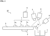
- FIG. 1 is a schematic view illustrating an example of a metal sorter according to an embodiment of the present invention.
- the present embodiment may separate non-metal objects 1b or metal objects 1a 1 , 1a 2 from the electronic and electrical device component scrap 1 containing at least the metal objects 1a 1 , 1a 2 and the non-metal objects 1b, for example using a metal sorter 10 as shown in FIG. 1 .
- FIG. 1 is merely illustrative, and the positions of the members and the positional relationship between the members are, of course, not limited to the example of FIG. 1 .
- the metal sorter 10 includes: a metal sensor 2; a color camera 3; an air valve 4; and a conveyor 5.
- a color camera lighting device 8 for illuminating a field of view of the color camera 3.
- a near-infrared sensor 6 may be further provided at a position facing the metal sensor 2 across the conveyor 5, in order to improve a detection efficiency.
- the metal sensor 2 of the metal sorter 10 detects the metal objects 1a 1 , 1a 2 on the conveyor 5.
- the conveyor 5 then conveys and releases the metal objects 1a 1 , 1a 2 and the non-metal objects 1b, and the color camera 3 arranged on the downstream side of the metal sensor 2 in the conveying direction receives light reflected by the metal objects 1a 1 , 1a 2 and the non-metal objects 1b struck by light emitted from the color camera lighting device 8 toward the optical detection position of the color camera 3 on a falling trajectory of the metal objects 1a 1 , 1a 2 and the non-metal objects 1b.
- a determination means (not shown) of the metal sorter 10 determines the positions of the non-metal objects 1b.
- the air valve 4 arranged on the downstream side of the optical detection position of the color camera 3 blows air to the non-metal objects 1b to shoot down the non-metal objects 1b, so that the non-metal objects 1b and the metal objects 1a 1 , 1a 2 will be housed in separate sorting containers 7, respectively.
- a general-purpose sensor for detecting metals can be employed.
- a sensor for detecting metals using electromagnetic induction can be preferably used.
- the metal sensor 2 including one or more electromagnetic induction coils (not shown) can be used, and the detection range of the metal sensor 2 can be changed depending on the sizes of the electromagnetic induction coils.
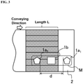
- FIG. 2 shows a schematic view illustrating a positional relationship between the detection range of the metal sensor 2 and the electronic and electrical device component scrap 1.
- the detection range of the metal sensor 2 has a width that is equal to that of the conveyor 5 (in an up-down direction on the paper surface of FIG. 2 ), and has a length L along a moving direction of the conveyor 5, i.e., the conveying direction of the electronic and electrical device component scrap 1.
- the non-metal object 1b sandwiched between the metal objects 1a 1 , 1a 2 may not be recognized as the non-metal objects 1b and may not be shot down by the air valve 4, when the non-metal object 1b is present between the metal objects 1a 1 and the metal object 1a 2 , as shown in FIG. 2 .
- a fixed distance d (the shortest distance) is preferably at least provided between the metal object 1a 1 and the metal object 1a 2 adjacent to each other, so as to prevent the non-metal object 1b present between the metal object 1a 1 and the metal objec 1a 2 adjacent to each other being form erroneously detected.
- the positions of the metal objects 1a 1 , 1a 2 are preferably adjusted such that the distance d between the metal object 1a 1 and the metal object 1a 2 with at least the non-metal object sandwiched between the metal object 1a 1 and the metal object 1a 2 is larger than the length L of the detection range of the metal sensor.
- the metal sensor 2 can recognize the metal object 1a 1 and the metal object 1a 2 as separate metal objects 1a 1 , 1a 2 , respectively, so that erroneous detection by the metal sensor 2 can be suppressed and the separation efficiency of the non-metal object 1b present between the metal objects 1a 1 , 1a 2 can be further improved. Even if the non-metal object 1b is not present between the metal object 1a 1 and the metal object 1a 2 , the fixed distance can be provided between the metal object 1a 1 and the metal object 1a 2 such that the fixed distance is larger than, specifically, the length L of the detection range of the metal sensor, so that a sorting efficiency between the metal objects 1a 1 , 1a 2 and the non-metal objects 1b can be improved.
- the metal sensor 2 may recognize the non-metal object 1b and the metal objects 1a 1 , 1a 2 as single metal object M as a whole, whereby the non-metal object 1b may not be recognized as a foreign matter and the non-metal object 1b may not be separated.
- the length L of the metal sensor 2 belongs to the device and is not particularly limited. However, since the characteristic particle diameter of the electronic and electrical device component scrap targeted by the present invention is typically from 4 to 70 mm or less, the length L may preferably be from 4 mm to 200 mm, and more preferably from 20 mm to 60 mm. Since the air valve 4 continues to blow air while the non-metal objects are flowing, the number of the air blowing is relatively low if the length L is equivalent to the size of the non-metal object in the electronic and electrical device component scrap, while the number of air blowing will be very high if the length L is too small, so that the air may be lacked during operation. Therefore, it is necessary to increase the capacity of a compressor in order to prevent the lack of air. Accordingly, the length L is preferably selected according to the size of the non-metal object in the electronic and electrical device component scrap.
- the metal objects 1a 1 , 1a 2 and the non-metal object 1b are previously dispersed on the conveyer 5, such as by vibrating the conveyor 5.
- a delivery speed of the conveyor 5 is 3 m/s in a fixed manner, but it may be in a variable manner. For example, it may vary between 1 and 5 m/s depending on the situations.
- the opening/closing speed of the air valve 4 is preferably from 0.5 to 4 ms/cycle, and more preferably from 2 to 4 ms/cycle.
- the metal sorter 10 can effectively sort the metal objects 1a 1 , 1a 2 including valuable metal-handling substrates containing a large amount of metal components such as wirings and leads on the surface or in the interior, and the non-metal objects 1b including the resin-handling substrates containing no metal or containing a trace amount of metal on the surface or in the interior.
- the sorted objects including the metal objects 1a 1 , 1a 2 can be processed as processing objects in a smelting step to improve a recovery efficiency of valuable metals.
- the separated objects separated as the non-metal objects 1b include the resin-handling substrates containing Sb that is a smelting inhibitor, substances that will inhibit the processing in the smelting step are prevented from being contaminated into the smelting step, so that a processing efficiency in the smelting process can be improved.
- Continuous processing using the metal sorter 10 as described above can allow efficient mechanical concentration of substrates that contain larger amounts of valuable metals from the electronic and electrical device component scrap, thereby improving a recovery efficiency of valuable metals while suppressing the contamination of the smelting inhibitors as compared with the conventional physical sorting step.
- the continuous processing of a large amount of electronic and electric device component scrap 1 leads to flying-up of powdery objects contained in the electronic and electric device component scrap 1 in the metal sorter 10 to adhere to peripheral equipment such as the color camera 3, the air valve 4, the near-infrared sensor 6, and the color camera lighting device 8, which causes a problem of malfunction (erroneous detection) of the metal sorter or troubles of the metal sorter 10.
- a step of removing powdery objects is carried out before the separation step of separating the metal objects 1a 1 , 1a 2 or the non-metal object 1b from the electronic and electrical device component scrap 1 containing the metal object 1a 1 , 1a 2 and the non-metal object 1b, using the metal sorter 10.
- This can allow the ratio of the powdery objects in the electronic and electrical device component scrap 1 fed into the metal sorter 10 to be reduced to suppress a decrease in recognition accuracy and sorting accuracy of the metal sorter 10, or erroneous recognition of the color camera 3 due to the flying-up of the powdery objects, so that the sorting efficiency of the metal sorter 10 can be improved.
- the powdery objects having a particle size of 5 mm or less enter the metal sorter 10.
- the "particle size" of the powdery objects refers to a median diameter of the powdery objects measured by a commercially available laser diffraction type particle size distribution measuring device.
- an amount of the powdery objects after the step of removing the powdery objects contained in the electronic and electrical device component scrap is 1% by mass with respect to the total amount of the electronic and electrical device component scrap before that step.
- wind power sorting As a specific method for removing the powdery objects, wind power sorting or sieve sorting is effective.
- the powdery objects are sorted as light weight objects.
- other component scrap such as aluminum pieces is also separated as the light weight objects. Therefore, if it is desired to selectively and efficiently separate only the powdery objects, an excessively high wind velocity is not desirable. Therefore, to achieve more efficient feeding of the powdery objects contained in the electronic and electrical device component scrap to the light weight object side by the wind power sorting, the wind power sorting is preferably carried out at a wind velocity of from 5.0 to 8.0 m/s, and more preferably from 6.0 to 7.0 m/s, as a condition for the wind power sorting.
- the wind power sorting can be carried out in at least two stages. For example, it is possible to combine a first wind sorting process for previously separating the powdery objects that will be affected on the failure of the metal sorter 10 with a second wind sorting process for concentrating the substrates fed to the metal sorter 10 and separating metals including Fe, Al, and the like.
- the second wind power sorting process for separating precious metal-containing objects such as substrates and ICs and metals including Fe, Al, and the like, from the electronic and electrical device component scrap 1 is preferably carried out at a wind velocity of from 10 to 18 m/s, or even from 15 to 18 m/s. In order to improve the concentration of capacitors and the fraction of metals, an optimum wind velocity is preferably from 5 to 15 m/s, of even from 8 to 12 m/s.
- the powdery objects can be separated to a sieved object side if a sieve opening is 2mm or more. If the sieve opening is too large, it can be adjusted, but other component scrap may be separated under the sieve. Therefore, it is desired to separate only the powdery objects, an excessive large sieve opening is not desirable. Therefore, the sieve opening is preferably from 2 mm to 5 mm. Further, if it is desired to remove wire-shaped scrap by the sieve sorting, a slit sieve is preferable, and it is also possible to remove the powdery objects together in this step.
- the wind power sorting or sieving process for removing the powdery objects may be carried out immediately before the processing with the metal sorter 10, or prior to this processing, it may be carried out in combination with any sorting stage.
- the wind power sorting may be carried out on the electronic and electrical device component scrap 1 immediately after at least one of the crushing, sieving, magnetic sorting, or color sorting processes that take place prior to the processing using the metal sorter 10, and the separation step may be then carried out using the metal sorter 10.
- the wind power sorting process or the sieving process may be carried out to remove the wire-shaped objects, which can also be included in the embodiment according to the present invention.
- the electronic and electrical device component scrap 1 is further subjected to a certain pre-processing prior to the processing by the metal sorter 10 according to the present embodiment, so that the sorting efficiency of the metal objects 1a 1 , 1a 2 and the non-metal objects 1b in the electronic and electrical device component scrap 1 can be further improved.
- the sorting efficiency of the metal objects 1a 1 , 1a 2 and the non-metal objects 1b can be improved by adjusting a number ratio (metal object/non-metal object) of the metal objects 1a 1 , 1a 2 to the non-metal objects 1b contained in the electronic and electrical device component scrap 1 so as to be 2.0 or less, or even 1.6 or less, or even 1.3 or less, before detecting the metal objects 1a 1 , 1a 2 in the electronic and electrical device component scrap 1 by the metal sensor 2.
- the adjustment can be efficiently carried out, for example, by using a color sorter provided with at least two camera units that can distinguish colors of both front and back sides of the processing object to sort substrate scrap in the electronic and electrical device component scrap.
- the present invention is not limited to each embodiment, and the components may be modified and embodied without departing from the spirit of the present invention. Further, various inventions may be created by appropriately combining the plurality of components disclosed in the present embodiment. For example, some components may be removed from all the components shown in the embodiments, or the components of different embodiments may be optionally combined.
Landscapes
- Engineering & Computer Science (AREA)
- Environmental & Geological Engineering (AREA)
- Chemical & Material Sciences (AREA)
- Materials Engineering (AREA)
- Metallurgy (AREA)
- Geology (AREA)
- Manufacturing & Machinery (AREA)
- General Life Sciences & Earth Sciences (AREA)
- Life Sciences & Earth Sciences (AREA)
- Mechanical Engineering (AREA)
- Geochemistry & Mineralogy (AREA)
- Organic Chemistry (AREA)
- Sorting Of Articles (AREA)
- Processing Of Solid Wastes (AREA)
- Combined Means For Separation Of Solids (AREA)
- Manufacture And Refinement Of Metals (AREA)
- Electrical Discharge Machining, Electrochemical Machining, And Combined Machining (AREA)
Applications Claiming Priority (2)
| Application Number | Priority Date | Filing Date | Title |
|---|---|---|---|
| JP2019069382A JP7076397B2 (ja) | 2019-03-29 | 2019-03-29 | 電子・電気機器部品屑の処理方法 |
| PCT/JP2020/014367 WO2020203918A1 (fr) | 2019-03-29 | 2020-03-27 | Procédé de traitement de déchets de composants de dispositifs électroniques/électriques |
Publications (2)
| Publication Number | Publication Date |
|---|---|
| EP3950153A1 true EP3950153A1 (fr) | 2022-02-09 |
| EP3950153A4 EP3950153A4 (fr) | 2022-11-30 |
Family
ID=72668677
Family Applications (1)
| Application Number | Title | Priority Date | Filing Date |
|---|---|---|---|
| EP20781759.4A Withdrawn EP3950153A4 (fr) | 2019-03-29 | 2020-03-27 | Procédé de traitement de déchets de composants de dispositifs électroniques/électriques |
Country Status (8)
| Country | Link |
|---|---|
| US (1) | US12036582B2 (fr) |
| EP (1) | EP3950153A4 (fr) |
| JP (1) | JP7076397B2 (fr) |
| KR (1) | KR102552541B1 (fr) |
| CN (1) | CN113631284A (fr) |
| CA (1) | CA3135438C (fr) |
| TW (1) | TWI767196B (fr) |
| WO (1) | WO2020203918A1 (fr) |
Cited By (1)
| Publication number | Priority date | Publication date | Assignee | Title |
|---|---|---|---|---|
| IT202200010550A1 (it) * | 2022-05-20 | 2023-11-20 | S T C S R L | Metodo per determinare una operazione di smaltimento di un prodotto elettronico |
Families Citing this family (1)
| Publication number | Priority date | Publication date | Assignee | Title |
|---|---|---|---|---|
| JP7264936B2 (ja) * | 2021-04-21 | 2023-04-25 | Jx金属株式会社 | 電気電子部品屑の処理方法及び電気電子部品屑の処理装置 |
Family Cites Families (24)
| Publication number | Priority date | Publication date | Assignee | Title |
|---|---|---|---|---|
| US4541530A (en) * | 1982-07-12 | 1985-09-17 | Magnetic Separation Systems, Inc. | Recovery of metallic concentrate from solid waste |
| US6060677A (en) * | 1994-08-19 | 2000-05-09 | Tiedemanns-Jon H. Andresen Ans | Determination of characteristics of material |
| JP3535629B2 (ja) | 1995-09-12 | 2004-06-07 | 日鉱金属株式会社 | スクラップ類からの有価金属のリサイクル方法 |
| JPH1057927A (ja) * | 1996-08-15 | 1998-03-03 | Nakajima Shoten:Kk | 複合廃棄物の処理方法 |
| JP2000343044A (ja) * | 1999-06-04 | 2000-12-12 | Hitachi Ltd | 物体の供給装置 |
| JP4554068B2 (ja) | 2000-12-28 | 2010-09-29 | 日鉱金属株式会社 | 樹脂付電子・電気部品からの金属の回収方法 |
| JP2002263581A (ja) | 2001-03-09 | 2002-09-17 | Ricoh Co Ltd | プラスチック製品リサイクル装置 |
| JP4424537B2 (ja) | 2004-03-17 | 2010-03-03 | ジェイティエンジニアリング株式会社 | 異物検査装置 |
| US7674994B1 (en) * | 2004-10-21 | 2010-03-09 | Valerio Thomas A | Method and apparatus for sorting metal |
| JP2007029923A (ja) | 2005-07-29 | 2007-02-08 | Mitsui Eng & Shipbuild Co Ltd | プリント基盤の回収方法 |
| CA2647700C (fr) * | 2006-03-31 | 2012-12-11 | Thomas Valerio | Procede et dispositif de tri de metaux non ferreux fins et d'elements de fils metallique isoles |
| JP2008142692A (ja) | 2006-11-17 | 2008-06-26 | Kitagawa Iron Works Co Ltd | 材料選別装置およびその方法 |
| WO2009152290A1 (fr) * | 2008-06-11 | 2009-12-17 | Valerio Thomas A | Procédé et système de récupération de métal à partir de matériaux recyclés traités |
| JP2011104461A (ja) | 2009-11-12 | 2011-06-02 | Panasonic Corp | 分別装置、及び、分別方法 |
| JP5705305B2 (ja) | 2011-03-29 | 2015-04-22 | 日本磁力選鉱株式会社 | 廃電子機器から有価金属を回収する方法 |
| JP5775752B2 (ja) | 2011-06-17 | 2015-09-09 | 三井金属鉱業株式会社 | 家電製品からの有価金属回収方法 |
| KR101090772B1 (ko) * | 2011-07-14 | 2011-12-08 | (주)한맥 | 유리 조각의 색상 선별 시스템 |
| JP6050222B2 (ja) | 2013-12-26 | 2016-12-21 | パンパシフィック・カッパー株式会社 | 電気・電子部品屑の処理方法 |
| JP7076178B2 (ja) | 2016-11-18 | 2022-05-27 | Jx金属株式会社 | 電子・電気機器部品屑の処理方法 |
| JP6846972B2 (ja) | 2017-03-30 | 2021-03-24 | Jx金属株式会社 | 部品付プリント基板の処理方法及び部品付プリント基板からの有価金属の回収方法 |
| JP2019048282A (ja) | 2017-09-12 | 2019-03-28 | 株式会社北川鉄工所 | 材料選別装置 |
| WO2019151351A1 (fr) | 2018-01-31 | 2019-08-08 | Jx金属株式会社 | Procédé de traitement de déchets de composants d'appareils électroniques et électriques |
| JP6914220B2 (ja) | 2018-03-16 | 2021-08-04 | Jx金属株式会社 | 電子・電気機器部品屑の処理方法 |
| KR20200129155A (ko) | 2018-03-16 | 2020-11-17 | 제이엑스금속주식회사 | 전자·전기 기기 부품 부스러기의 처리 방법 |
-
2019
- 2019-03-29 JP JP2019069382A patent/JP7076397B2/ja active Active
-
2020
- 2020-03-09 TW TW109107597A patent/TWI767196B/zh active
- 2020-03-27 EP EP20781759.4A patent/EP3950153A4/fr not_active Withdrawn
- 2020-03-27 US US17/599,226 patent/US12036582B2/en active Active
- 2020-03-27 CN CN202080024370.2A patent/CN113631284A/zh active Pending
- 2020-03-27 KR KR1020217032920A patent/KR102552541B1/ko active Active
- 2020-03-27 CA CA3135438A patent/CA3135438C/fr active Active
- 2020-03-27 WO PCT/JP2020/014367 patent/WO2020203918A1/fr not_active Ceased
Cited By (2)
| Publication number | Priority date | Publication date | Assignee | Title |
|---|---|---|---|---|
| IT202200010550A1 (it) * | 2022-05-20 | 2023-11-20 | S T C S R L | Metodo per determinare una operazione di smaltimento di un prodotto elettronico |
| WO2023223240A1 (fr) * | 2022-05-20 | 2023-11-23 | S.T.C. S.R.L. | Procédé de détermination d'une opération d'élimination d'un produit électronique, programme informatique, unité de commande et système |
Also Published As
| Publication number | Publication date |
|---|---|
| CA3135438C (fr) | 2024-05-14 |
| EP3950153A4 (fr) | 2022-11-30 |
| TW202039108A (zh) | 2020-11-01 |
| KR20210137175A (ko) | 2021-11-17 |
| CA3135438A1 (fr) | 2020-10-08 |
| KR102552541B1 (ko) | 2023-07-07 |
| JP2020163353A (ja) | 2020-10-08 |
| TWI767196B (zh) | 2022-06-11 |
| WO2020203918A1 (fr) | 2020-10-08 |
| US12036582B2 (en) | 2024-07-16 |
| JP7076397B2 (ja) | 2022-05-27 |
| CN113631284A (zh) | 2021-11-09 |
| US20220176415A1 (en) | 2022-06-09 |
Similar Documents
| Publication | Publication Date | Title |
|---|---|---|
| US11554388B2 (en) | Method for processing electronic and electrical device component scrap | |
| KR102591293B1 (ko) | 전자ㆍ전기 기기 부품 스크랩의 처리 방법 및 처리 장치 | |
| CA3090225C (fr) | Procede de traitement de dechets de composants d'appareils electroniques et electriques | |
| US12036582B2 (en) | Method for processing electronic/electrical device component scraps | |
| JP2021191578A (ja) | 電子・電気機器部品屑の処理方法 | |
| CA3094156C (fr) | Procede de traitement de dechets de composants de dispositif electroniques et electriques | |
| JP7029333B2 (ja) | 電子・電気機器部品屑の処理方法 | |
| JP6885904B2 (ja) | 電子・電気機器部品屑の処理方法 | |
| JP7123839B2 (ja) | 電子・電気機器部品屑の処理方法 | |
| JP2019171342A (ja) | 電子・電気機器部品屑の処理方法 |
Legal Events
| Date | Code | Title | Description |
|---|---|---|---|
| STAA | Information on the status of an ep patent application or granted ep patent |
Free format text: STATUS: THE INTERNATIONAL PUBLICATION HAS BEEN MADE |
|
| PUAI | Public reference made under article 153(3) epc to a published international application that has entered the european phase |
Free format text: ORIGINAL CODE: 0009012 |
|
| STAA | Information on the status of an ep patent application or granted ep patent |
Free format text: STATUS: REQUEST FOR EXAMINATION WAS MADE |
|
| 17P | Request for examination filed |
Effective date: 20211005 |
|
| AK | Designated contracting states |
Kind code of ref document: A1 Designated state(s): AL AT BE BG CH CY CZ DE DK EE ES FI FR GB GR HR HU IE IS IT LI LT LU LV MC MK MT NL NO PL PT RO RS SE SI SK SM TR |
|
| DAV | Request for validation of the european patent (deleted) | ||
| DAX | Request for extension of the european patent (deleted) | ||
| A4 | Supplementary search report drawn up and despatched |
Effective date: 20221103 |
|
| RIC1 | Information provided on ipc code assigned before grant |
Ipc: B07B 4/08 20060101ALI20221027BHEP Ipc: B07B 4/02 20060101ALI20221027BHEP Ipc: B03B 4/00 20060101ALI20221027BHEP Ipc: B09B 5/00 20060101ALI20221027BHEP Ipc: B07B 7/00 20060101AFI20221027BHEP |
|
| STAA | Information on the status of an ep patent application or granted ep patent |
Free format text: STATUS: THE APPLICATION HAS BEEN WITHDRAWN |
|
| 18W | Application withdrawn |
Effective date: 20240404 |