EP3955295A1 - Structure semi-conductrice et procédé de préchauffage associé - Google Patents
Structure semi-conductrice et procédé de préchauffage associé Download PDFInfo
- Publication number
- EP3955295A1 EP3955295A1 EP20926529.7A EP20926529A EP3955295A1 EP 3955295 A1 EP3955295 A1 EP 3955295A1 EP 20926529 A EP20926529 A EP 20926529A EP 3955295 A1 EP3955295 A1 EP 3955295A1
- Authority
- EP
- European Patent Office
- Prior art keywords
- chip
- storage
- control
- semiconductor structure
- temperature detection
- Prior art date
- Legal status (The legal status is an assumption and is not a legal conclusion. Google has not performed a legal analysis and makes no representation as to the accuracy of the status listed.)
- Granted
Links
Images


Classifications
-
- H—ELECTRICITY
- H10—SEMICONDUCTOR DEVICES; ELECTRIC SOLID-STATE DEVICES NOT OTHERWISE PROVIDED FOR
- H10B—ELECTRONIC MEMORY DEVICES
- H10B12/00—Dynamic random access memory [DRAM] devices
-
- G—PHYSICS
- G11—INFORMATION STORAGE
- G11C—STATIC STORES
- G11C7/00—Arrangements for writing information into, or reading information out from, a digital store
- G11C7/04—Arrangements for writing information into, or reading information out from, a digital store with means for avoiding disturbances due to temperature effects
-
- G—PHYSICS
- G11—INFORMATION STORAGE
- G11C—STATIC STORES
- G11C11/00—Digital stores characterised by the use of particular electric or magnetic storage elements; Storage elements therefor
- G11C11/21—Digital stores characterised by the use of particular electric or magnetic storage elements; Storage elements therefor using electric elements
- G11C11/34—Digital stores characterised by the use of particular electric or magnetic storage elements; Storage elements therefor using electric elements using semiconductor devices
- G11C11/40—Digital stores characterised by the use of particular electric or magnetic storage elements; Storage elements therefor using electric elements using semiconductor devices using transistors
- G11C11/401—Digital stores characterised by the use of particular electric or magnetic storage elements; Storage elements therefor using electric elements using semiconductor devices using transistors forming cells needing refreshing or charge regeneration, i.e. dynamic cells
- G11C11/4063—Auxiliary circuits, e.g. for addressing, decoding, driving, writing, sensing or timing
- G11C11/407—Auxiliary circuits, e.g. for addressing, decoding, driving, writing, sensing or timing for memory cells of the field-effect type
- G11C11/4072—Circuits for initialization, powering up or down, clearing memory or presetting
-
- G—PHYSICS
- G11—INFORMATION STORAGE
- G11C—STATIC STORES
- G11C11/00—Digital stores characterised by the use of particular electric or magnetic storage elements; Storage elements therefor
- G11C11/21—Digital stores characterised by the use of particular electric or magnetic storage elements; Storage elements therefor using electric elements
- G11C11/34—Digital stores characterised by the use of particular electric or magnetic storage elements; Storage elements therefor using electric elements using semiconductor devices
- G11C11/40—Digital stores characterised by the use of particular electric or magnetic storage elements; Storage elements therefor using electric elements using semiconductor devices using transistors
- G11C11/401—Digital stores characterised by the use of particular electric or magnetic storage elements; Storage elements therefor using electric elements using semiconductor devices using transistors forming cells needing refreshing or charge regeneration, i.e. dynamic cells
-
- G—PHYSICS
- G11—INFORMATION STORAGE
- G11C—STATIC STORES
- G11C7/00—Arrangements for writing information into, or reading information out from, a digital store
- G11C7/20—Memory cell initialisation circuits, e.g. when powering up or down, memory clear, latent image memory
-
- H—ELECTRICITY
- H10—SEMICONDUCTOR DEVICES; ELECTRIC SOLID-STATE DEVICES NOT OTHERWISE PROVIDED FOR
- H10W—GENERIC PACKAGES, INTERCONNECTIONS, CONNECTORS OR OTHER CONSTRUCTIONAL DETAILS OF DEVICES COVERED BY CLASS H10
- H10W90/00—Package configurations
-
- G—PHYSICS
- G11—INFORMATION STORAGE
- G11C—STATIC STORES
- G11C11/00—Digital stores characterised by the use of particular electric or magnetic storage elements; Storage elements therefor
- G11C11/21—Digital stores characterised by the use of particular electric or magnetic storage elements; Storage elements therefor using electric elements
- G11C11/34—Digital stores characterised by the use of particular electric or magnetic storage elements; Storage elements therefor using electric elements using semiconductor devices
- G11C11/40—Digital stores characterised by the use of particular electric or magnetic storage elements; Storage elements therefor using electric elements using semiconductor devices using transistors
- G11C11/401—Digital stores characterised by the use of particular electric or magnetic storage elements; Storage elements therefor using electric elements using semiconductor devices using transistors forming cells needing refreshing or charge regeneration, i.e. dynamic cells
- G11C11/4063—Auxiliary circuits, e.g. for addressing, decoding, driving, writing, sensing or timing
- G11C11/407—Auxiliary circuits, e.g. for addressing, decoding, driving, writing, sensing or timing for memory cells of the field-effect type
- G11C11/4076—Timing circuits
-
- G—PHYSICS
- G11—INFORMATION STORAGE
- G11C—STATIC STORES
- G11C5/00—Details of stores covered by group G11C11/00
- G11C5/02—Disposition of storage elements, e.g. in the form of a matrix array
- G11C5/025—Geometric lay-out considerations of storage- and peripheral-blocks in a semiconductor storage device
-
- G—PHYSICS
- G11—INFORMATION STORAGE
- G11C—STATIC STORES
- G11C5/00—Details of stores covered by group G11C11/00
- G11C5/02—Disposition of storage elements, e.g. in the form of a matrix array
- G11C5/04—Supports for storage elements, e.g. memory modules; Mounting or fixing of storage elements on such supports
-
- H—ELECTRICITY
- H10—SEMICONDUCTOR DEVICES; ELECTRIC SOLID-STATE DEVICES NOT OTHERWISE PROVIDED FOR
- H10W—GENERIC PACKAGES, INTERCONNECTIONS, CONNECTORS OR OTHER CONSTRUCTIONAL DETAILS OF DEVICES COVERED BY CLASS H10
- H10W90/00—Package configurations
- H10W90/20—Configurations of stacked chips
- H10W90/284—Configurations of stacked chips characterised by structural arrangements for measuring or testing
-
- H—ELECTRICITY
- H10—SEMICONDUCTOR DEVICES; ELECTRIC SOLID-STATE DEVICES NOT OTHERWISE PROVIDED FOR
- H10W—GENERIC PACKAGES, INTERCONNECTIONS, CONNECTORS OR OTHER CONSTRUCTIONAL DETAILS OF DEVICES COVERED BY CLASS H10
- H10W90/00—Package configurations
- H10W90/20—Configurations of stacked chips
- H10W90/288—Configurations of stacked chips characterised by arrangements for thermal management of the stacked chips
-
- H—ELECTRICITY
- H10—SEMICONDUCTOR DEVICES; ELECTRIC SOLID-STATE DEVICES NOT OTHERWISE PROVIDED FOR
- H10W—GENERIC PACKAGES, INTERCONNECTIONS, CONNECTORS OR OTHER CONSTRUCTIONAL DETAILS OF DEVICES COVERED BY CLASS H10
- H10W90/00—Package configurations
- H10W90/20—Configurations of stacked chips
- H10W90/297—Configurations of stacked chips characterised by the through-semiconductor vias [TSVs] in the stacked chips
Definitions
- the present disclosure relates to the field of memory, and in particular, to a semiconductor structure and a preheating method thereof.
- a dynamic random-access memory is a semiconductor storage device commonly used in a computer.
- the storage array of the DRAM includes many duplicate storage units.
- Each storage unit usually includes a capacitor and a transistor.
- the gate of the transistor is connected to a word line
- the drain of the transistor is connected to a bit line
- the source of the transistor is connected to the capacitor.
- the voltage signal on the word line can control the ON or OFF of the transistor, and data can subsequently be read from or written into the capacitor through the bit line.
- a low temperature may prolong the write time for writing data into a memory and adversely affect the stability of the data to be written.
- the technical problem to be solved by the present disclosure is how to reduce write time in writing data into a memory at a low temperature and improve the stability of the data to be written.
- the semiconductor structure includes a storage chip, a temperature detection unit, and a control chip.
- the temperature detection unit is configured to detect the temperature of the storage chip before the storage chip initiates.
- the control chip is configured to, before the storage chip initiates, heat the storage chip, determine whether the temperature detected by the temperature detection unit reaches a specified threshold, and, in response to the temperature reaching the specified threshold, control the storage chip to initiate.
- the semiconductor structure may include one or more storage chips.
- the semiconductor structure may include two or more storage chips, the two or more storage chips may be sequentially stacked vertically.
- the one or more storage chips may be located on the control chip and electrically connected to the control chip.
- the semiconductor structure may further include a line substrate.
- the line substrate may have a connection line.
- the one or more storage chips and the control chip may both be located on the line substrate, and the one or more storage chips and the control chip may be connected through the connection line in the line substrate.
- the semiconductor structure may include one or more temperature detection units electrically connected to the control chip.
- the one or more temperature detection units may be in the control chip, in the one or more storage chips, or on the line substrate between the one or more storage chips and the control chip.
- the semiconductor structure may include only one temperature detection unit.
- the control chip may be configured to: upon determining that the temperature detected by the temperature detection unit reaches the specified threshold, control all the one or more storage chips to initiate.
- the semiconductor structure may include only one temperature detection unit and two or more storage chips.
- the control chip may be configured to: upon determining that the temperature detected by the temperature detection unit reaches the specified threshold, first, control a storage chip closest to the control chip to initiate, and then control other storage chips on the storage chip to sequentially initiate.
- the semiconductor structure may include two or more temperature detection units and two or more storage chips.
- Each storage chip may have one temperature detection unit.
- the control chip may be configured to: sequentially determine whether a respective temperature detected by each of the temperature detection units reaches the specified threshold; and, in response to the temperature detected by one of the temperature detection units reaching the specified threshold, control the storage chip corresponding to the temperature detection unit to initiate.
- control chip is further configured to: after the storage chip initiates, control the storage chip to perform write, read, and erase operations.
- control chip may initiate before the control chip heats the storage chip, and the control chip may be configured to: heat the storage chip using heat generated by the control chip after the control chip initiates.
- control chip may have a heating circuit configured to heat the storage chip.
- control chip may be configured to: before or after the control chip heats the storage chip, determine whether the temperature of the storage chip detected by the temperature detection unit reaches the specified threshold; and, in response to the temperature not reaching the specified threshold, control the heating circuit to heat the storage chip; or, in response to the temperature reaching the specified threshold, control the heating circuit to stop heating the storage chip.
- the storage chip may be a Dynamic Random Access Memory (DRAM) storage chip.
- DRAM Dynamic Random Access Memory
- the method includes providing a semiconductor structure, where the semiconductor structure includes a storage chip, a control chip electrically connected to the storage chip, and a temperature detection unit; initiating the control chip; heating, by the control chip and before the storage chip initiates, the storage chip; detecting a temperature of the storage chip by the temperature detection unit; and determining, by the control chip, whether the temperature detected by the temperature detection unit reaches a specified threshold; and, in response to the temperature reaching the specified threshold, initiating the storage chip.
- the semiconductor structure may include one or more temperature detection units and one or more storage chips.
- the semiconductor structure may include two or more storage chips, the two or more storage chips may be sequentially stacked vertically.
- the semiconductor structure may include only one temperature detection unit.
- the control chip may be configured to: upon determining that the temperature detected by the temperature detection unit reaches the specified threshold, control all the one or more storage chips to initiate.
- the semiconductor structure may include only one temperature detection unit and two or more storage chips.
- the control chip is configured to: upon determining that the temperature detected by the temperature detection unit reaches the specified threshold, first, control the storage chip closest to the control chip to initiate, and then control other storage chips on the storage chip to sequentially initiate.
- the semiconductor structure may include two or more temperature detection units and two or more storage chips.
- Each storage chip may have one temperature detection unit.
- the control chip may be configured to: sequentially determine whether a respective temperature detected by each of the temperature detection units reaches the specified threshold; and, in response to the temperature detected by one of the temperature detection units reaching the specified threshold, control the storage chip corresponding to the temperature detection unit to initiate.
- control chip is further configured to: after the storage chip initiates, control the storage chip to perform write, read, and erase operations.
- the semiconductor structure provided in the present disclosure may include a storage chip, a temperature detection unit, and a control chip.
- the temperature detection unit may be configured to detect the temperature of the storage chip before the storage chip initiates.
- the control chip may be configured to, before the storage chip initiates, heat the storage chip and determine whether the temperature detected by the temperature detection unit reaches a specified threshold; and, if the temperature reaches the specified threshold, control the storage chip to initiate.
- the control chip may be configured to cooperate with the temperature detection unit.
- the control chip may heat the storage chip before the storage chip initiates.
- the temperature detection unit may detect the temperature of the storage chip before the storage chip initiates.
- control chip may determine whether the temperature detected by the temperature detection unit reaches the specified threshold, and, if the temperature reaches the specified threshold, control the storage chip to initiate. Therefore, when the semiconductor structure provided in the present disclosure works at a low temperature, the storage chip may be heated to the specified threshold by the control chip, thereby preventing an increase of the resistances of the bit line, the word line, and the metal connection line (metal contact part) in the storage chip due to an excessively low temperature, reducing the write time for writing data into the memory at the low temperature and improving the write stability of the memory.
- the semiconductor structure may include only one temperature detection unit.
- the temperature detection unit may be in the control chip, in the one or more storage chips, or on the line substrate between the one or more storage chips and the control chip.
- the control chip may be configured to: upon determining that the temperature detected by the temperature detection unit reaches the specified threshold, control all the storage chips to initiate.
- the aforementioned control structure and control manner may be relatively simple, and may reduce the write time for writing data into the storage chip at a low temperature and improve the write stability of the storage chip.
- the semiconductor structure may include only one temperature detection unit and two or more storage chips.
- the control chip may be configured to: upon determining that the temperature detected by the temperature detection unit reaches the specified threshold, first, control the storage chip closest to the control chip to initiate, and then control other storage chips on the storage chip to sequentially initiate.
- the aforementioned control structure and control manner may cause each storage chip to initiate after reaching the specified threshold, thereby improving the precision of the initiation of each storage chip, reducing the write time for writing data into each storage chip at a low temperature and improving the write stability of each storage chip.
- the semiconductor structure may include two or more temperature detection units and two or more storage chips.
- Each storage chip may have one temperature detection unit.
- the control chip may be configured to: sequentially determine whether a respective temperature detected by each of the temperature detection units reaches the specified threshold; and, in response to the temperature detected by one of the temperature detection units reaching the specified threshold, control the storage chip corresponding to the temperature detection unit to initiate.
- the aforementioned control structure and control manner may further improve the precision of the initiation of each storage chip, thereby reducing the write time for writing data into each storage chip at a low temperature and further improving the write stability of each storage chip.
- control chip may initiate before the control chip heat the storage chip. And the control chip may heat the storage chip using heat generated by the control chip after the control chip initiates. Therefore, no additional heating circuit may be needed, thereby simplifying the semiconductor structure.
- the control chip may have an additional heating circuit configured to heat the storage chip. Before or after the control chip heats the storage chip, the control chip may be configured to determine whether the temperature of the storage chip detected by the temperature detection unit reaches the specified threshold. If the temperature does not reach the specified threshold, the control chip may control the heating circuit to heat the storage chip. If the temperature reaches the specified threshold, the control chip may control the heating circuit to stop heating the storage chip. Therefore, the heating process may be accurately controlled, so that the temperature of the storage chip can be kept near the specified threshold, thereby preventing the temperature of the storage chip from being excessively high or excessively low, and always keeping the write time of the memory relatively short.
- the storage chip before a storage chip initiates, the storage chip may be heated by a control chip.
- the temperature of the storage chip may be detected by a temperature detection unit.
- the control chip may be configured to determine whether the temperature detected by the temperature detection unit reaches a specified threshold. If the temperature reaches the specified threshold, the storage chip may be controlled to initiate. Therefore, when the semiconductor structure provided in the present disclosure works at a low temperature, the storage chip may be heated to the specified threshold by using the control chip, thereby preventing an increase of the resistances of the bit line, the word line, and the metal connection line (metal contact part) in the storage chip due to an excessively low temperature, reducing the write time for writing data into the memory at the low temperature and improving the write stability of the memory.
- a lower temperature may prolong the write time for writing data into a memory and adversely affect the stability of the data to be written.
- the present disclosure presents a semiconductor structure and a preheating method thereof to address the foregoing issues.
- the semiconductor structure may include a storage chip, a temperature detection unit, and a control chip.
- the temperature detection unit may be configured to detect the temperature of the storage chip before the storage chip initiates.
- the control chip may be configured to, before the storage chip initiates, heat the storage chip and determine whether the temperature detected by the temperature detection unit reaches a specified threshold, and, if the temperature reaches the specified threshold, control the storage chip to initiate.
- the control chip may be configured to cooperate with the temperature detection unit.
- the control chip may heat the storage chip before the storage chip initiates.
- the temperature detection unit may detect the temperature of the storage chip before the storage chip initiates.
- the control chip may determine whether the temperature detected by the temperature detection unit reaches the specified threshold. If the temperature reaches the specified threshold, the control chip may control the storage chip to initiate.
- the storage chip may be heated to the specified threshold by the control chip, thereby preventing an increase of the resistances of the bit line, the word line, and the metal connection line (metal contact part) in the storage chip due to an excessively low temperature, reducing the write time for writing data into the memory at the low temperature and improving the write stability of the memory.
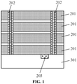
- FIGs. 1 , 2 , 3 , 4 , 5 , 6 , and 7 are schematic structural diagrams of a semiconductor structure according to one or more embodiments of the present disclosure.
- FIG. 8 is a schematic flowchart of a semiconductor structure preheating method according to one or more embodiments of the present disclosure.
- the semiconductor structure may include a storage chip 201, a temperature detection unit 203, and a control chip 301.
- the temperature detection unit 203 may be configured to detect the temperature of the storage chip 201 before the storage chip 201 initiates.
- the control chip 301 may be configured to, before the storage chip 201 initiates, heat the storage chip 201 and determine whether the temperature detected by the temperature detection unit 203 reaches a specified threshold, and, if the temperature reaches the specified threshold, control the storage chip 201 to initiate.
- the storage chip 201 may be a memory that can perform data write, data read, and/or data deletion.
- the storage chip 201 may be formed by using a semiconductor integrated production process.
- the storage chip 201 may include a storage array and a peripheral circuit connected to the storage array.
- the storage array may include several storage units, and a bit line, a word line, and a metal connection line (metal contact part) that are connected to each storage unit.
- the storage unit may be configured to store data.
- the peripheral circuit may be a related circuit used when performing an operation on the storage array.
- the storage chip 201 may be a DRAM storage chip.
- the DRAM storage chip may include several storage units. Each of the storage units may include a capacitor and a transistor. The gate of the transistor may be connected to a word line, the drain of the transistor may be connected to a bit line, and the source of the transistor may be connected to the capacitor.
- the storage chip 201 may be other types of storage chips.
- the number of storage chips 201 may be at least 1. Specifically, the number of storage chips 201 may be 1 or greater than or equal to 2. When the number of storage chips is greater than or equal to 2, the storage chips may be sequentially stacked vertically to form a stacked storage chip structure. Referring to FIG. 2 , in some embodiments, the number of storage chips 201 may be 4. The four storage chips 201 may be sequentially stacked from bottom to top to form a stacked storage chip structure. Adjacent storage chips 201 may be bonded together through a bonding process or an adhering process. In some embodiments, a through-silicon via (TSV) may be formed in the storage chip 201.
- TSV through-silicon via
- the storage chip 201 may be electrically connected to the control chip 301 through the through-silicon via (TSV). When multiple storage chips 201 are stacked, each storage chip 201 may be connected to the control chip 301 through a different through-silicon via (TSV). In some embodiments, the storage chip 201 may be alternatively connected to the control chip 301 by using a metal lead (formed by a lead bonding process).
- the storage chip 201 may be located on the control chip 301 and electrically connected to the control chip 301.
- the control chip 301 may be bonded to the storage chip 201.
- the control chip 301 may be bonded to the storage chip 201 at the bottom layer in the stacked structure.
- the storage chip 201 and the control chip 301 may be connected in different manners.
- the semiconductor structure may further include a line substrate 401.
- the line substrate 401 may have a connection line.
- the storage chip 201 and the control chip 301 may both be located on the line substrate 401, and the storage chip 201 and the control chip 301 may be connected by using the connection line in the line substrate 401.
- the line substrate 401 may be a PCB substrate.
- the control chip 301 may be formed by using the semiconductor integrated production process.
- the control chip 301 may be configured to heat the storage chip 201, so that the temperature of the storage chip 201 can reach the specified threshold.
- the specified threshold may be set in the control chip 301 based on an actual need or experience.
- the control chip 301 may be further configured to control the initiation of the storage chip 201 and perfrom related operations on the storage chip 201.
- the initiation of the strorage chip may include power-on and self-testing.
- the performing of related operations on the storage chip 201 may include writing data into the storage chip 201, reading data from the storage chip 201, deleting data stored in the storage chip 201, and the like.
- the semiconductor structure may further include the temperature detection unit 203.
- the temperature detection unit 203 may be configured to measure the temperature of the storage chip 201 before the storage chip 201 initiates.
- the temperature detection unit 203 may be electrically connected to the control chip 301.
- the temperature detected by the temperature detection unit 203 may be sent to the control chip 301, and may serve as the basis for controlling, by the control chip 301, the storage chip 201 to initiate.
- the control chip 301 may be configured to cooperate with the temperature detection unit 203.
- the control chip 301 may heat the storage chip 201 before the storage chip 201 initiates.
- the temperature detection unit 203 may detect the temperature of the storage chip 201 before the storage chip 201 initiates.
- control chip 301 may determine whether the temperature detected by the temperature detection unit 203 reaches the specified threshold, and, if the temperature reaches the specified threshold, control the storage chip 201 to initiate. Therefore, when the semiconductor structure provided in the present disclosure works at a low temperature, the storage chip 201 may be heated to the specified threshold by using the control chip 301, thereby preventing an increase of the resistances of the bit line, the word line, and the metal connection line (metal contact part) in the storage chip due to an excessively low temperature, reducing the write time for writing data into the memory at the low temperature, and improving the write stability of the memory.
- the temperature detection unit 203 may include a temperature sensor.
- the temperature sensor may be configured to sense a temperature and convert the sensed temperature into an electrical signal.
- the temperature sensor may be a P-N junction temperature sensor or a capacitive temperature sensor.
- the temperature sensor may be formed by using the semiconductor integrated production process, and may be located in the storage chip 201, in the control chip 301, or located on the line substrate 401 between the storage chip 201 and the control chip 301, as shown in FIG. 5 .
- the number of temperature detection units 203 may be 1 or greater than or equal to 2.
- the temperature detection unit 203 may be in the control chip 301 or in the storage chip 201.
- the number of temperature detection units 203 may be 1. Specifically, the temperature detection unit 203 may be in the control chip 301, as shown in FIGs. 1 and 4 . Alternatively, the temperature detection unit 203 may be in the storage chip 201. When there is only one storage chip 201, the temperature detection unit 203 may be directly located in the storage chip 201. When there are multiple storage chips 201 forming a stacked structure, the temperature detection unit 203 may be located in one of the storage chips 201, and may be preferably located in the storage chip 201 at the bottom layer in the stacked structure, as shown in FIGs. 2 and 6 . The temperature detection unit 203 may be on the line substrate 401 between the storage chip 201 and the control chip 301, as shown in FIG. 5 .
- the control chip 301 may control all storage chips 201 to initiate.
- the aforementioned control structure and control manner may be relatively simple, and may reduce the write time for writing data into the storage chip 201 at a low temperature and improve the write stability of the storage chip 201.
- the number of temperature detection units 203 may be 1 and the number of storage chips 201 may be greater than or equal to 2.
- the control chip 301 may first control the storage chip 201 closest to the control chip 301 to initiate, and then control other storage chips 201 above the storae chip 201 to sequentially initiate. Referring to FIG. 1 (or referring to FIGs. 2 , 4 , 5 , and 6 ), the number of temperature detection units 203 may be 1 and the number of storage chips 201 may be greater than or equal to 2.
- the control chip 301 may first control the storage chip 201 closest to the control chip 301 to initiate, and then control other storage chips 201 above the storae chip 201 to sequentially initiate. Referring to FIG.
- the control chip 301 may first control the storage chip 201 closest to the control chip 301 (the storage chip at the bottom layer in the stacked structure) to initiate, and then control the other three storage chips 201 above to sequentially initiate.
- the aforementioned control structure and control manner may cause each storage chip 201 to initiate after the specified threshold temperature is reached, thereby improving the precision of the initiation of each storage chip 201, reducing the write time for writing data into each storage chip 201 at a low temperature and improving the write stability of each storage chip 201.
- the number of temperature detection units 203 may be greater than or equal to 2 and the number of storage chips 201 may be greater than or equal to 2.
- Each storage chip 201 may have one temperature detection unit 203.
- the control chip 301 may sequentially determine whether a respective temperature detected by each of the temperature detection units 203 reaches the specified threshold, and, if the temperature detected by one of the temperature detection units 203 reaches the specified threshold, control the storage chip corresponding to the temperature detection unit 203 to initiate.
- each temperature detection unit 203 may detect a respective temperature of a corresponding storage chip 201, thereby obtaining four detected temperatures.
- the control chip 301 may sequentially determine whether a respective temperature detected by each of the four temperature detection units 203 reaches the specified threshold, and, if the temperature detected by one of the temperature detection units 203 reaches the specified threshold, control the storage chip corresponding to the temperature detection unit 203 to initiate. For example, when the temperature detected by the temperature detection unit 203 in the storage chip 201 at the bottom layer in the stacked structure first reaches the specified threshold, the control chip 301 may first control the storage chip 201 at the bottom layer in the stacked structure to initiate.
- the control chip 301 may control the storage chip 201 at the penultimate layer in the stacked structure to initiate.
- the initiation of the storage chips 201 on the two upper layers may be conducted in the same manner.
- the aforementioned control structure and control manner may further improve the precision of the of each storage chip 201, reduce the write time for writing data into each storage chip 201 at a low temperature and improve the write stability of each storage chip 201.
- the control chip 301 may need to initiate.
- the control chip 301 may need to be powered on and self-tested.
- the control chip 301 may not give an instruction to the storage chip 201. Only when the temperature detected by the temperature detection unit reaches the specified threshold, the control chip 301 may control the storage chip 201 to initiate.
- the control chip 301 may heat the storage chip using the heat generated by the control chip 301 after the control chip 301 initiates. Therefore, no additional heating circuit may be needed, thereby simplifying the semiconductor structure.
- control chip 301 may further control the storage chip 201 to perform write, read, and erase operations.
- the control chip 301 may have a control circuit.
- the control circuit may be configured to control the storage chip 201 to initiate and control the storage chip 201 to perform write, read, and erase operations.
- the control chip 301 may have a heating circuit, configured to heat the storage chip 201. Before or after the control chip 301 heats the storage chip 201, the control chip may determine whether the temperature of the storage chip detected by the temperature detection unit reaches the specified threshold. If the temperature does not reach the specified threshold, the control chip may control the heating circuit to heat the storage chip. If the temperature reaches the specified threshold, the control chip may control the heating circuit to stop heating the storage chip. Therefore, the heating process may be accurately controlled, so that the temperature of the storage chip 201 can be kept near the specified threshold, thereby preventing the temperature of the storage chip 201 from being excessively high or low, and preventing the write time of the memory from being prolonged under undesirable temperatures.
- This invention further presents a semiconductor structure preheating method.
- the method may include the following steps S101 through S105.
- a semiconductor structure may be provided.
- the semiconductor structure may include a storage chip, a control chip electrically connected to the storage chip, and a temperature detection unit.
- control chip may initiate.
- the storage chip may be heated by the control chip.
- the temperature of the storage chip may be detected by the temperature detection unit.
- control chip may determine whether the temperature detected by the temperature detection unit reaches a specified threshold, and, if the temperature reaches the specified threshold, control the storage chip to initiate.
- the number of temperature detection units may be 1 or greater than or equal to 2
- the number of storage chips may be 1 or greater than or equal to 2.
- the number of storage chips is greater than or equal to 2
- several storage chips may be sequentially stacked vertically.
- the number of temperature detection units may be 1. Upon determining that the temperature detected by the temperature detection unit reaches the specified threshold, the control chip may control all storage chips to initiate.
- the number of temperature detection units may be 1 and the number of storage chips may be greater than or equal to 2.
- the control chip may first control the storage chip closest to the control chip to initiate, and then control other storage chips above the storage chip to sequentially initiate.
- the number of temperature detection units may be greater than or equal to 2 and the number of storage chips may be greater than or equal to 2.
- Each storage chip may have one temperature detection unit.
- the control chip may sequentially determine whether a respective temperature detected by each of the temperature detection units reaches the specified threshold, and, if the temperature detected by one of the temperature detection units reaches the specified threshold, control the storage chip corresponding to the temperature detection unit to initiate.
- control chip may further control the storage chip to perform write, read, and erase operations.
Landscapes
- Engineering & Computer Science (AREA)
- Microelectronics & Electronic Packaging (AREA)
- Computer Hardware Design (AREA)
- Dram (AREA)
- Semiconductor Memories (AREA)
- Read Only Memory (AREA)
Applications Claiming Priority (2)
| Application Number | Priority Date | Filing Date | Title |
|---|---|---|---|
| CN202010216794.0A CN113451309B (zh) | 2020-03-25 | 2020-03-25 | 半导体结构及其预热方法 |
| PCT/CN2020/131414 WO2021189887A1 (fr) | 2020-03-25 | 2020-11-25 | Structure semi-conductrice et procédé de préchauffage associé |
Publications (3)
| Publication Number | Publication Date |
|---|---|
| EP3955295A1 true EP3955295A1 (fr) | 2022-02-16 |
| EP3955295A4 EP3955295A4 (fr) | 2022-08-24 |
| EP3955295B1 EP3955295B1 (fr) | 2024-05-01 |
Family
ID=77807528
Family Applications (1)
| Application Number | Title | Priority Date | Filing Date |
|---|---|---|---|
| EP20926529.7A Active EP3955295B1 (fr) | 2020-03-25 | 2020-11-25 | Structure semi-conductrice et procédé de préchauffage associé |
Country Status (4)
| Country | Link |
|---|---|
| US (1) | US11862223B2 (fr) |
| EP (1) | EP3955295B1 (fr) |
| CN (1) | CN113451309B (fr) |
| WO (1) | WO2021189887A1 (fr) |
Families Citing this family (6)
| Publication number | Priority date | Publication date | Assignee | Title |
|---|---|---|---|---|
| US20240087636A1 (en) * | 2022-09-08 | 2024-03-14 | Advanced Micro Devices, Inc. | Dynamic Memory Operations |
| CN115525459A (zh) * | 2022-09-16 | 2022-12-27 | 山东云海国创云计算装备产业创新中心有限公司 | 一种设备初始化的方法、装置及介质 |
| CN116185511A (zh) * | 2023-03-02 | 2023-05-30 | 湖南泽天智航电子技术有限公司 | 一种基于飞腾x100芯片的低温启动系统及方法 |
| CN115981735A (zh) * | 2023-03-17 | 2023-04-18 | 广州匠芯创科技有限公司 | 芯片的低温启动控制方法及其系统、电子设备、存储介质 |
| CN116880625B (zh) * | 2023-09-07 | 2023-12-05 | 北京华鲲振宇智能科技有限责任公司 | 一种智能融合终端整机cpu芯片低温加热装置及方法 |
| WO2025101831A1 (fr) * | 2023-11-09 | 2025-05-15 | MTS IP Holdings Ltd | Systèmes de gestion thermique et d'énergie dans des circuits intégrés tridimensionnels |
Family Cites Families (19)
| Publication number | Priority date | Publication date | Assignee | Title |
|---|---|---|---|---|
| US6393374B1 (en) * | 1999-03-30 | 2002-05-21 | Intel Corporation | Programmable thermal management of an integrated circuit die |
| JP2001160042A (ja) * | 1999-12-02 | 2001-06-12 | Mitsubishi Electric Corp | 温度センサ搭載のマイクロコンピュータ |
| DE10122363B4 (de) * | 2001-05-09 | 2007-11-29 | Infineon Technologies Ag | Halbleitermodul |
| DE10313605B4 (de) * | 2003-03-26 | 2009-03-19 | Qimonda Ag | Vorrichtung und Verfahren zum Steuern mehrerer Speicherbausteine |
| JP2008065430A (ja) * | 2006-09-05 | 2008-03-21 | Matsushita Electric Ind Co Ltd | 半導体装置およびicカード |
| JP2008117195A (ja) * | 2006-11-06 | 2008-05-22 | Hitachi Ltd | 半導体記憶装置 |
| US7760569B2 (en) * | 2007-04-05 | 2010-07-20 | Qimonda Ag | Semiconductor memory device with temperature control |
| CN101866690B (zh) * | 2009-04-14 | 2013-07-24 | 宏碁股份有限公司 | 一种利用薄膜电晶体作为非易失性存储器的方法 |
| US9274805B2 (en) * | 2012-02-24 | 2016-03-01 | Qualcomm Incorporated | System and method for thermally aware device booting |
| US10371745B2 (en) * | 2014-01-23 | 2019-08-06 | Micron Technology, Inc. | Overheat protection circuit and method in an accelerated aging test of an integrated circuit |
| US9668337B2 (en) | 2015-09-08 | 2017-05-30 | Western Digital Technologies, Inc. | Temperature management in data storage devices |
| US10564900B2 (en) * | 2016-03-04 | 2020-02-18 | Western Digital Technologies, Inc. | Temperature variation compensation |
| US9996281B2 (en) * | 2016-03-04 | 2018-06-12 | Western Digital Technologies, Inc. | Temperature variation compensation |
| JP6756965B2 (ja) * | 2016-12-09 | 2020-09-16 | 富士通株式会社 | 半導体装置及び半導体装置の制御方法 |
| TWI659311B (zh) * | 2018-05-14 | 2019-05-11 | 慧榮科技股份有限公司 | 資料儲存系統以及非揮發式記憶體操作方法 |
| CN211507637U (zh) * | 2020-03-25 | 2020-09-15 | 长鑫存储技术有限公司 | 半导体结构 |
| CN212303079U (zh) * | 2020-07-17 | 2021-01-05 | 长鑫存储技术有限公司 | 半导体装置 |
| CN212303077U (zh) * | 2020-07-17 | 2021-01-05 | 长鑫存储技术有限公司 | 半导体装置 |
| CN212303078U (zh) * | 2020-07-17 | 2021-01-05 | 长鑫存储技术有限公司 | 半导体装置 |
-
2020
- 2020-03-25 CN CN202010216794.0A patent/CN113451309B/zh active Active
- 2020-11-25 WO PCT/CN2020/131414 patent/WO2021189887A1/fr not_active Ceased
- 2020-11-25 EP EP20926529.7A patent/EP3955295B1/fr active Active
-
2021
- 2021-08-07 US US17/396,686 patent/US11862223B2/en active Active
Also Published As
| Publication number | Publication date |
|---|---|
| EP3955295A4 (fr) | 2022-08-24 |
| WO2021189887A1 (fr) | 2021-09-30 |
| EP3955295B1 (fr) | 2024-05-01 |
| CN113451309A (zh) | 2021-09-28 |
| US20210366531A1 (en) | 2021-11-25 |
| CN113451309B (zh) | 2025-01-14 |
| US11862223B2 (en) | 2024-01-02 |
Similar Documents
| Publication | Publication Date | Title |
|---|---|---|
| EP3955295A1 (fr) | Structure semi-conductrice et procédé de préchauffage associé | |
| KR102326562B1 (ko) | 테스트부를 갖는 반도체 장치, 이를 포함하는 전자 장치 및 그 테스트 방법 | |
| CN211507637U (zh) | 半导体结构 | |
| KR20130044655A (ko) | 반도체 소자 및 제조 방법 | |
| US20250053332A1 (en) | Read retry method for enhancing read performance and stability of 3d nand memory | |
| US11862229B2 (en) | Reading and writing method of memory device and memory device | |
| EP4053692B1 (fr) | Dispositif de stockage de mémoire, procédé de fonctionnement du dispositif de stockage et procédé de fonctionnement d'un dispositif hôte | |
| CN113945293B (zh) | 半导体装置 | |
| CN113870916B (zh) | 半导体装置 | |
| EP3961633B1 (fr) | Dispositif à semi-conducteur | |
| US11832382B2 (en) | Printed circuit board and a storage system including the same | |
| CN114141287B (zh) | 存储装置的读写方法及存储装置 | |
| US20240431112A1 (en) | Memory device and method of manufacturing the same | |
| EP3968324B1 (fr) | Dispositif à semi-conducteur | |
| KR20250065064A (ko) | 쉴딩 비트라인들을 제어하는 메모리 장치 | |
| KR20250084634A (ko) | 메모리 장치 및 이의 제조 방법 | |
| KR102386476B1 (ko) | 반도체 장치 및 그의 구동 방법 |
Legal Events
| Date | Code | Title | Description |
|---|---|---|---|
| STAA | Information on the status of an ep patent application or granted ep patent |
Free format text: STATUS: THE INTERNATIONAL PUBLICATION HAS BEEN MADE |
|
| PUAI | Public reference made under article 153(3) epc to a published international application that has entered the european phase |
Free format text: ORIGINAL CODE: 0009012 |
|
| STAA | Information on the status of an ep patent application or granted ep patent |
Free format text: STATUS: REQUEST FOR EXAMINATION WAS MADE |
|
| 17P | Request for examination filed |
Effective date: 20211112 |
|
| AK | Designated contracting states |
Kind code of ref document: A1 Designated state(s): AL AT BE BG CH CY CZ DE DK EE ES FI FR GB GR HR HU IE IS IT LI LT LU LV MC MK MT NL NO PL PT RO RS SE SI SK SM TR |
|
| REG | Reference to a national code |
Ref country code: DE Ref legal event code: R079 Free format text: PREVIOUS MAIN CLASS: H01L0027108000 Ipc: G11C0007040000 Ref country code: DE Ref legal event code: R079 Ref document number: 602020030445 Country of ref document: DE Free format text: PREVIOUS MAIN CLASS: H01L0027108000 Ipc: G11C0007040000 |
|
| A4 | Supplementary search report drawn up and despatched |
Effective date: 20220725 |
|
| RIC1 | Information provided on ipc code assigned before grant |
Ipc: H01L 27/108 20060101ALN20220719BHEP Ipc: H01L 25/18 20060101ALN20220719BHEP Ipc: H01L 25/16 20060101ALN20220719BHEP Ipc: H01L 25/065 20060101ALN20220719BHEP Ipc: G11C 11/4076 20060101ALN20220719BHEP Ipc: G11C 5/04 20060101ALN20220719BHEP Ipc: G11C 5/02 20060101ALN20220719BHEP Ipc: G11C 11/4072 20060101ALI20220719BHEP Ipc: G11C 7/20 20060101ALI20220719BHEP Ipc: G11C 7/04 20060101AFI20220719BHEP |
|
| STAA | Information on the status of an ep patent application or granted ep patent |
Free format text: STATUS: EXAMINATION IS IN PROGRESS |
|
| 17Q | First examination report despatched |
Effective date: 20230209 |
|
| DAV | Request for validation of the european patent (deleted) | ||
| DAX | Request for extension of the european patent (deleted) | ||
| GRAP | Despatch of communication of intention to grant a patent |
Free format text: ORIGINAL CODE: EPIDOSNIGR1 |
|
| STAA | Information on the status of an ep patent application or granted ep patent |
Free format text: STATUS: GRANT OF PATENT IS INTENDED |
|
| RIC1 | Information provided on ipc code assigned before grant |
Ipc: H01L 25/18 20060101ALN20240108BHEP Ipc: H01L 25/16 20060101ALN20240108BHEP Ipc: H01L 25/065 20060101ALN20240108BHEP Ipc: G11C 11/4076 20060101ALN20240108BHEP Ipc: G11C 5/04 20060101ALN20240108BHEP Ipc: G11C 5/02 20060101ALN20240108BHEP Ipc: G11C 11/4072 20060101ALI20240108BHEP Ipc: G11C 7/20 20060101ALI20240108BHEP Ipc: G11C 7/04 20060101AFI20240108BHEP |
|
| INTG | Intention to grant announced |
Effective date: 20240122 |
|
| P01 | Opt-out of the competence of the unified patent court (upc) registered |
Effective date: 20240214 |
|
| GRAS | Grant fee paid |
Free format text: ORIGINAL CODE: EPIDOSNIGR3 |
|
| GRAA | (expected) grant |
Free format text: ORIGINAL CODE: 0009210 |
|
| STAA | Information on the status of an ep patent application or granted ep patent |
Free format text: STATUS: THE PATENT HAS BEEN GRANTED |
|
| AK | Designated contracting states |
Kind code of ref document: B1 Designated state(s): AL AT BE BG CH CY CZ DE DK EE ES FI FR GB GR HR HU IE IS IT LI LT LU LV MC MK MT NL NO PL PT RO RS SE SI SK SM TR |
|
| REG | Reference to a national code |
Ref country code: GB Ref legal event code: FG4D |
|
| REG | Reference to a national code |
Ref country code: CH Ref legal event code: EP |
|
| REG | Reference to a national code |
Ref country code: DE Ref legal event code: R096 Ref document number: 602020030445 Country of ref document: DE |
|
| REG | Reference to a national code |
Ref country code: IE Ref legal event code: FG4D |
|
| REG | Reference to a national code |
Ref country code: LT Ref legal event code: MG9D |
|
| REG | Reference to a national code |
Ref country code: NL Ref legal event code: MP Effective date: 20240501 |
|
| PG25 | Lapsed in a contracting state [announced via postgrant information from national office to epo] |
Ref country code: IS Free format text: LAPSE BECAUSE OF FAILURE TO SUBMIT A TRANSLATION OF THE DESCRIPTION OR TO PAY THE FEE WITHIN THE PRESCRIBED TIME-LIMIT Effective date: 20240901 |
|
| PG25 | Lapsed in a contracting state [announced via postgrant information from national office to epo] |
Ref country code: BG Free format text: LAPSE BECAUSE OF FAILURE TO SUBMIT A TRANSLATION OF THE DESCRIPTION OR TO PAY THE FEE WITHIN THE PRESCRIBED TIME-LIMIT Effective date: 20240501 |
|
| PG25 | Lapsed in a contracting state [announced via postgrant information from national office to epo] |
Ref country code: FI Free format text: LAPSE BECAUSE OF FAILURE TO SUBMIT A TRANSLATION OF THE DESCRIPTION OR TO PAY THE FEE WITHIN THE PRESCRIBED TIME-LIMIT Effective date: 20240501 Ref country code: HR Free format text: LAPSE BECAUSE OF FAILURE TO SUBMIT A TRANSLATION OF THE DESCRIPTION OR TO PAY THE FEE WITHIN THE PRESCRIBED TIME-LIMIT Effective date: 20240501 |
|
| PG25 | Lapsed in a contracting state [announced via postgrant information from national office to epo] |
Ref country code: GR Free format text: LAPSE BECAUSE OF FAILURE TO SUBMIT A TRANSLATION OF THE DESCRIPTION OR TO PAY THE FEE WITHIN THE PRESCRIBED TIME-LIMIT Effective date: 20240802 |
|
| PG25 | Lapsed in a contracting state [announced via postgrant information from national office to epo] |
Ref country code: PT Free format text: LAPSE BECAUSE OF FAILURE TO SUBMIT A TRANSLATION OF THE DESCRIPTION OR TO PAY THE FEE WITHIN THE PRESCRIBED TIME-LIMIT Effective date: 20240902 |
|
| REG | Reference to a national code |
Ref country code: AT Ref legal event code: MK05 Ref document number: 1683542 Country of ref document: AT Kind code of ref document: T Effective date: 20240501 |
|
| PG25 | Lapsed in a contracting state [announced via postgrant information from national office to epo] |
Ref country code: NL Free format text: LAPSE BECAUSE OF FAILURE TO SUBMIT A TRANSLATION OF THE DESCRIPTION OR TO PAY THE FEE WITHIN THE PRESCRIBED TIME-LIMIT Effective date: 20240501 |
|
| PG25 | Lapsed in a contracting state [announced via postgrant information from national office to epo] |
Ref country code: ES Free format text: LAPSE BECAUSE OF FAILURE TO SUBMIT A TRANSLATION OF THE DESCRIPTION OR TO PAY THE FEE WITHIN THE PRESCRIBED TIME-LIMIT Effective date: 20240501 |
|
| PG25 | Lapsed in a contracting state [announced via postgrant information from national office to epo] |
Ref country code: AT Free format text: LAPSE BECAUSE OF FAILURE TO SUBMIT A TRANSLATION OF THE DESCRIPTION OR TO PAY THE FEE WITHIN THE PRESCRIBED TIME-LIMIT Effective date: 20240501 |
|
| PG25 | Lapsed in a contracting state [announced via postgrant information from national office to epo] |
Ref country code: PL Free format text: LAPSE BECAUSE OF FAILURE TO SUBMIT A TRANSLATION OF THE DESCRIPTION OR TO PAY THE FEE WITHIN THE PRESCRIBED TIME-LIMIT Effective date: 20240501 |
|
| PG25 | Lapsed in a contracting state [announced via postgrant information from national office to epo] |
Ref country code: LV Free format text: LAPSE BECAUSE OF FAILURE TO SUBMIT A TRANSLATION OF THE DESCRIPTION OR TO PAY THE FEE WITHIN THE PRESCRIBED TIME-LIMIT Effective date: 20240501 |
|
| PG25 | Lapsed in a contracting state [announced via postgrant information from national office to epo] |
Ref country code: PT Free format text: LAPSE BECAUSE OF FAILURE TO SUBMIT A TRANSLATION OF THE DESCRIPTION OR TO PAY THE FEE WITHIN THE PRESCRIBED TIME-LIMIT Effective date: 20240902 Ref country code: PL Free format text: LAPSE BECAUSE OF FAILURE TO SUBMIT A TRANSLATION OF THE DESCRIPTION OR TO PAY THE FEE WITHIN THE PRESCRIBED TIME-LIMIT Effective date: 20240501 Ref country code: NO Free format text: LAPSE BECAUSE OF FAILURE TO SUBMIT A TRANSLATION OF THE DESCRIPTION OR TO PAY THE FEE WITHIN THE PRESCRIBED TIME-LIMIT Effective date: 20240801 Ref country code: NL Free format text: LAPSE BECAUSE OF FAILURE TO SUBMIT A TRANSLATION OF THE DESCRIPTION OR TO PAY THE FEE WITHIN THE PRESCRIBED TIME-LIMIT Effective date: 20240501 Ref country code: LV Free format text: LAPSE BECAUSE OF FAILURE TO SUBMIT A TRANSLATION OF THE DESCRIPTION OR TO PAY THE FEE WITHIN THE PRESCRIBED TIME-LIMIT Effective date: 20240501 Ref country code: IS Free format text: LAPSE BECAUSE OF FAILURE TO SUBMIT A TRANSLATION OF THE DESCRIPTION OR TO PAY THE FEE WITHIN THE PRESCRIBED TIME-LIMIT Effective date: 20240901 Ref country code: HR Free format text: LAPSE BECAUSE OF FAILURE TO SUBMIT A TRANSLATION OF THE DESCRIPTION OR TO PAY THE FEE WITHIN THE PRESCRIBED TIME-LIMIT Effective date: 20240501 Ref country code: GR Free format text: LAPSE BECAUSE OF FAILURE TO SUBMIT A TRANSLATION OF THE DESCRIPTION OR TO PAY THE FEE WITHIN THE PRESCRIBED TIME-LIMIT Effective date: 20240802 Ref country code: FI Free format text: LAPSE BECAUSE OF FAILURE TO SUBMIT A TRANSLATION OF THE DESCRIPTION OR TO PAY THE FEE WITHIN THE PRESCRIBED TIME-LIMIT Effective date: 20240501 Ref country code: ES Free format text: LAPSE BECAUSE OF FAILURE TO SUBMIT A TRANSLATION OF THE DESCRIPTION OR TO PAY THE FEE WITHIN THE PRESCRIBED TIME-LIMIT Effective date: 20240501 Ref country code: BG Free format text: LAPSE BECAUSE OF FAILURE TO SUBMIT A TRANSLATION OF THE DESCRIPTION OR TO PAY THE FEE WITHIN THE PRESCRIBED TIME-LIMIT Effective date: 20240501 Ref country code: AT Free format text: LAPSE BECAUSE OF FAILURE TO SUBMIT A TRANSLATION OF THE DESCRIPTION OR TO PAY THE FEE WITHIN THE PRESCRIBED TIME-LIMIT Effective date: 20240501 Ref country code: RS Free format text: LAPSE BECAUSE OF FAILURE TO SUBMIT A TRANSLATION OF THE DESCRIPTION OR TO PAY THE FEE WITHIN THE PRESCRIBED TIME-LIMIT Effective date: 20240801 |
|
| PG25 | Lapsed in a contracting state [announced via postgrant information from national office to epo] |
Ref country code: DK Free format text: LAPSE BECAUSE OF FAILURE TO SUBMIT A TRANSLATION OF THE DESCRIPTION OR TO PAY THE FEE WITHIN THE PRESCRIBED TIME-LIMIT Effective date: 20240501 |
|
| PG25 | Lapsed in a contracting state [announced via postgrant information from national office to epo] |
Ref country code: EE Free format text: LAPSE BECAUSE OF FAILURE TO SUBMIT A TRANSLATION OF THE DESCRIPTION OR TO PAY THE FEE WITHIN THE PRESCRIBED TIME-LIMIT Effective date: 20240501 |
|
| PG25 | Lapsed in a contracting state [announced via postgrant information from national office to epo] |
Ref country code: CZ Free format text: LAPSE BECAUSE OF FAILURE TO SUBMIT A TRANSLATION OF THE DESCRIPTION OR TO PAY THE FEE WITHIN THE PRESCRIBED TIME-LIMIT Effective date: 20240501 |
|
| PG25 | Lapsed in a contracting state [announced via postgrant information from national office to epo] |
Ref country code: SK Free format text: LAPSE BECAUSE OF FAILURE TO SUBMIT A TRANSLATION OF THE DESCRIPTION OR TO PAY THE FEE WITHIN THE PRESCRIBED TIME-LIMIT Effective date: 20240501 Ref country code: RO Free format text: LAPSE BECAUSE OF FAILURE TO SUBMIT A TRANSLATION OF THE DESCRIPTION OR TO PAY THE FEE WITHIN THE PRESCRIBED TIME-LIMIT Effective date: 20240501 |
|
| PG25 | Lapsed in a contracting state [announced via postgrant information from national office to epo] |
Ref country code: SM Free format text: LAPSE BECAUSE OF FAILURE TO SUBMIT A TRANSLATION OF THE DESCRIPTION OR TO PAY THE FEE WITHIN THE PRESCRIBED TIME-LIMIT Effective date: 20240501 |
|
| PG25 | Lapsed in a contracting state [announced via postgrant information from national office to epo] |
Ref country code: SM Free format text: LAPSE BECAUSE OF FAILURE TO SUBMIT A TRANSLATION OF THE DESCRIPTION OR TO PAY THE FEE WITHIN THE PRESCRIBED TIME-LIMIT Effective date: 20240501 Ref country code: SK Free format text: LAPSE BECAUSE OF FAILURE TO SUBMIT A TRANSLATION OF THE DESCRIPTION OR TO PAY THE FEE WITHIN THE PRESCRIBED TIME-LIMIT Effective date: 20240501 Ref country code: RO Free format text: LAPSE BECAUSE OF FAILURE TO SUBMIT A TRANSLATION OF THE DESCRIPTION OR TO PAY THE FEE WITHIN THE PRESCRIBED TIME-LIMIT Effective date: 20240501 Ref country code: EE Free format text: LAPSE BECAUSE OF FAILURE TO SUBMIT A TRANSLATION OF THE DESCRIPTION OR TO PAY THE FEE WITHIN THE PRESCRIBED TIME-LIMIT Effective date: 20240501 Ref country code: DK Free format text: LAPSE BECAUSE OF FAILURE TO SUBMIT A TRANSLATION OF THE DESCRIPTION OR TO PAY THE FEE WITHIN THE PRESCRIBED TIME-LIMIT Effective date: 20240501 Ref country code: CZ Free format text: LAPSE BECAUSE OF FAILURE TO SUBMIT A TRANSLATION OF THE DESCRIPTION OR TO PAY THE FEE WITHIN THE PRESCRIBED TIME-LIMIT Effective date: 20240501 |
|
| REG | Reference to a national code |
Ref country code: DE Ref legal event code: R097 Ref document number: 602020030445 Country of ref document: DE |
|
| PG25 | Lapsed in a contracting state [announced via postgrant information from national office to epo] |
Ref country code: IT Free format text: LAPSE BECAUSE OF FAILURE TO SUBMIT A TRANSLATION OF THE DESCRIPTION OR TO PAY THE FEE WITHIN THE PRESCRIBED TIME-LIMIT Effective date: 20240501 |
|
| PLBE | No opposition filed within time limit |
Free format text: ORIGINAL CODE: 0009261 |
|
| STAA | Information on the status of an ep patent application or granted ep patent |
Free format text: STATUS: NO OPPOSITION FILED WITHIN TIME LIMIT |
|
| 26N | No opposition filed |
Effective date: 20250204 |
|
| PG25 | Lapsed in a contracting state [announced via postgrant information from national office to epo] |
Ref country code: SI Free format text: LAPSE BECAUSE OF FAILURE TO SUBMIT A TRANSLATION OF THE DESCRIPTION OR TO PAY THE FEE WITHIN THE PRESCRIBED TIME-LIMIT Effective date: 20240501 |
|
| REG | Reference to a national code |
Ref country code: CH Ref legal event code: PL |
|
| PG25 | Lapsed in a contracting state [announced via postgrant information from national office to epo] |
Ref country code: MC Free format text: LAPSE BECAUSE OF FAILURE TO SUBMIT A TRANSLATION OF THE DESCRIPTION OR TO PAY THE FEE WITHIN THE PRESCRIBED TIME-LIMIT Effective date: 20240501 |
|
| PG25 | Lapsed in a contracting state [announced via postgrant information from national office to epo] |
Ref country code: LU Free format text: LAPSE BECAUSE OF NON-PAYMENT OF DUE FEES Effective date: 20241125 |
|
| REG | Reference to a national code |
Ref country code: CH Ref legal event code: PL |
|
| GBPC | Gb: european patent ceased through non-payment of renewal fee |
Effective date: 20241125 |
|
| PG25 | Lapsed in a contracting state [announced via postgrant information from national office to epo] |
Ref country code: CH Free format text: LAPSE BECAUSE OF NON-PAYMENT OF DUE FEES Effective date: 20241130 |
|
| REG | Reference to a national code |
Ref country code: BE Ref legal event code: MM Effective date: 20241130 |
|
| PG25 | Lapsed in a contracting state [announced via postgrant information from national office to epo] |
Ref country code: SE Free format text: LAPSE BECAUSE OF FAILURE TO SUBMIT A TRANSLATION OF THE DESCRIPTION OR TO PAY THE FEE WITHIN THE PRESCRIBED TIME-LIMIT Effective date: 20240501 |
|
| PG25 | Lapsed in a contracting state [announced via postgrant information from national office to epo] |
Ref country code: GB Free format text: LAPSE BECAUSE OF NON-PAYMENT OF DUE FEES Effective date: 20241125 Ref country code: BE Free format text: LAPSE BECAUSE OF NON-PAYMENT OF DUE FEES Effective date: 20241130 |
|
| PG25 | Lapsed in a contracting state [announced via postgrant information from national office to epo] |
Ref country code: FR Free format text: LAPSE BECAUSE OF NON-PAYMENT OF DUE FEES Effective date: 20241130 |
|
| PG25 | Lapsed in a contracting state [announced via postgrant information from national office to epo] |
Ref country code: IE Free format text: LAPSE BECAUSE OF NON-PAYMENT OF DUE FEES Effective date: 20241125 |
|
| PGFP | Annual fee paid to national office [announced via postgrant information from national office to epo] |
Ref country code: DE Payment date: 20251119 Year of fee payment: 6 |
|
| PG25 | Lapsed in a contracting state [announced via postgrant information from national office to epo] |
Ref country code: HU Free format text: LAPSE BECAUSE OF FAILURE TO SUBMIT A TRANSLATION OF THE DESCRIPTION OR TO PAY THE FEE WITHIN THE PRESCRIBED TIME-LIMIT; INVALID AB INITIO Effective date: 20201125 |
|
| PG25 | Lapsed in a contracting state [announced via postgrant information from national office to epo] |
Ref country code: CY Free format text: LAPSE BECAUSE OF FAILURE TO SUBMIT A TRANSLATION OF THE DESCRIPTION OR TO PAY THE FEE WITHIN THE PRESCRIBED TIME-LIMIT; INVALID AB INITIO Effective date: 20201125 |