EP3955312A1 - Transistor à haute mobilité de trous (hhmt) et son procédé de fabrication - Google Patents
Transistor à haute mobilité de trous (hhmt) et son procédé de fabrication Download PDFInfo
- Publication number
- EP3955312A1 EP3955312A1 EP19923756.1A EP19923756A EP3955312A1 EP 3955312 A1 EP3955312 A1 EP 3955312A1 EP 19923756 A EP19923756 A EP 19923756A EP 3955312 A1 EP3955312 A1 EP 3955312A1
- Authority
- EP
- European Patent Office
- Prior art keywords
- layer
- electrode
- channel
- mobility transistor
- hole mobility
- Prior art date
- Legal status (The legal status is an assumption and is not a legal conclusion. Google has not performed a legal analysis and makes no representation as to the accuracy of the status listed.)
- Granted
Links
Images






Classifications
-
- H—ELECTRICITY
- H10—SEMICONDUCTOR DEVICES; ELECTRIC SOLID-STATE DEVICES NOT OTHERWISE PROVIDED FOR
- H10D—INORGANIC ELECTRIC SEMICONDUCTOR DEVICES
- H10D30/00—Field-effect transistors [FET]
- H10D30/40—FETs having zero-dimensional [0D], one-dimensional [1D] or two-dimensional [2D] charge carrier gas channels
- H10D30/47—FETs having zero-dimensional [0D], one-dimensional [1D] or two-dimensional [2D] charge carrier gas channels having two-dimensional [2D] charge carrier gas channels, e.g. nanoribbon FETs or high electron mobility transistors [HEMT]
- H10D30/471—High electron mobility transistors [HEMT] or high hole mobility transistors [HHMT]
- H10D30/475—High electron mobility transistors [HEMT] or high hole mobility transistors [HHMT] having wider bandgap layer formed on top of lower bandgap active layer, e.g. undoped barrier HEMTs such as i-AlGaN/GaN HEMTs
-
- H—ELECTRICITY
- H10—SEMICONDUCTOR DEVICES; ELECTRIC SOLID-STATE DEVICES NOT OTHERWISE PROVIDED FOR
- H10D—INORGANIC ELECTRIC SEMICONDUCTOR DEVICES
- H10D84/00—Integrated devices formed in or on semiconductor substrates that comprise only semiconducting layers, e.g. on Si wafers or on GaAs-on-Si wafers
- H10D84/80—Integrated devices formed in or on semiconductor substrates that comprise only semiconducting layers, e.g. on Si wafers or on GaAs-on-Si wafers characterised by the integration of at least one component covered by groups H10D12/00 or H10D30/00, e.g. integration of IGFETs
- H10D84/82—Integrated devices formed in or on semiconductor substrates that comprise only semiconducting layers, e.g. on Si wafers or on GaAs-on-Si wafers characterised by the integration of at least one component covered by groups H10D12/00 or H10D30/00, e.g. integration of IGFETs of only field-effect components
-
- H—ELECTRICITY
- H10—SEMICONDUCTOR DEVICES; ELECTRIC SOLID-STATE DEVICES NOT OTHERWISE PROVIDED FOR
- H10D—INORGANIC ELECTRIC SEMICONDUCTOR DEVICES
- H10D84/00—Integrated devices formed in or on semiconductor substrates that comprise only semiconducting layers, e.g. on Si wafers or on GaAs-on-Si wafers
- H10D84/80—Integrated devices formed in or on semiconductor substrates that comprise only semiconducting layers, e.g. on Si wafers or on GaAs-on-Si wafers characterised by the integration of at least one component covered by groups H10D12/00 or H10D30/00, e.g. integration of IGFETs
- H10D84/82—Integrated devices formed in or on semiconductor substrates that comprise only semiconducting layers, e.g. on Si wafers or on GaAs-on-Si wafers characterised by the integration of at least one component covered by groups H10D12/00 or H10D30/00, e.g. integration of IGFETs of only field-effect components
- H10D84/83—Integrated devices formed in or on semiconductor substrates that comprise only semiconducting layers, e.g. on Si wafers or on GaAs-on-Si wafers characterised by the integration of at least one component covered by groups H10D12/00 or H10D30/00, e.g. integration of IGFETs of only field-effect components of only insulated-gate FETs [IGFET]
- H10D84/85—Complementary IGFETs, e.g. CMOS
-
- H—ELECTRICITY
- H10—SEMICONDUCTOR DEVICES; ELECTRIC SOLID-STATE DEVICES NOT OTHERWISE PROVIDED FOR
- H10D—INORGANIC ELECTRIC SEMICONDUCTOR DEVICES
- H10D30/00—Field-effect transistors [FET]
- H10D30/01—Manufacture or treatment
- H10D30/015—Manufacture or treatment of FETs having heterojunction interface channels or heterojunction gate electrodes, e.g. HEMT
-
- H—ELECTRICITY
- H10—SEMICONDUCTOR DEVICES; ELECTRIC SOLID-STATE DEVICES NOT OTHERWISE PROVIDED FOR
- H10D—INORGANIC ELECTRIC SEMICONDUCTOR DEVICES
- H10D30/00—Field-effect transistors [FET]
- H10D30/40—FETs having zero-dimensional [0D], one-dimensional [1D] or two-dimensional [2D] charge carrier gas channels
- H10D30/47—FETs having zero-dimensional [0D], one-dimensional [1D] or two-dimensional [2D] charge carrier gas channels having two-dimensional [2D] charge carrier gas channels, e.g. nanoribbon FETs or high electron mobility transistors [HEMT]
- H10D30/471—High electron mobility transistors [HEMT] or high hole mobility transistors [HHMT]
- H10D30/477—Vertical HEMTs or vertical HHMTs
-
- H—ELECTRICITY
- H10—SEMICONDUCTOR DEVICES; ELECTRIC SOLID-STATE DEVICES NOT OTHERWISE PROVIDED FOR
- H10D—INORGANIC ELECTRIC SEMICONDUCTOR DEVICES
- H10D30/00—Field-effect transistors [FET]
- H10D30/40—FETs having zero-dimensional [0D], one-dimensional [1D] or two-dimensional [2D] charge carrier gas channels
- H10D30/47—FETs having zero-dimensional [0D], one-dimensional [1D] or two-dimensional [2D] charge carrier gas channels having two-dimensional [2D] charge carrier gas channels, e.g. nanoribbon FETs or high electron mobility transistors [HEMT]
- H10D30/471—High electron mobility transistors [HEMT] or high hole mobility transistors [HHMT]
- H10D30/478—High electron mobility transistors [HEMT] or high hole mobility transistors [HHMT] the 2D charge carrier gas being at least partially not parallel to a main surface of the semiconductor body
-
- H—ELECTRICITY
- H10—SEMICONDUCTOR DEVICES; ELECTRIC SOLID-STATE DEVICES NOT OTHERWISE PROVIDED FOR
- H10D—INORGANIC ELECTRIC SEMICONDUCTOR DEVICES
- H10D62/00—Semiconductor bodies, or regions thereof, of devices having potential barriers
- H10D62/10—Shapes, relative sizes or dispositions of the regions of the semiconductor bodies; Shapes of the semiconductor bodies
- H10D62/117—Shapes of semiconductor bodies
-
- H—ELECTRICITY
- H10—SEMICONDUCTOR DEVICES; ELECTRIC SOLID-STATE DEVICES NOT OTHERWISE PROVIDED FOR
- H10D—INORGANIC ELECTRIC SEMICONDUCTOR DEVICES
- H10D62/00—Semiconductor bodies, or regions thereof, of devices having potential barriers
- H10D62/40—Crystalline structures
- H10D62/405—Orientations of crystalline planes
-
- H—ELECTRICITY
- H10—SEMICONDUCTOR DEVICES; ELECTRIC SOLID-STATE DEVICES NOT OTHERWISE PROVIDED FOR
- H10D—INORGANIC ELECTRIC SEMICONDUCTOR DEVICES
- H10D62/00—Semiconductor bodies, or regions thereof, of devices having potential barriers
- H10D62/80—Semiconductor bodies, or regions thereof, of devices having potential barriers characterised by the materials
- H10D62/83—Semiconductor bodies, or regions thereof, of devices having potential barriers characterised by the materials being Group IV materials, e.g. B-doped Si or undoped Ge
- H10D62/832—Semiconductor bodies, or regions thereof, of devices having potential barriers characterised by the materials being Group IV materials, e.g. B-doped Si or undoped Ge being Group IV materials comprising two or more elements, e.g. SiGe
- H10D62/8325—Silicon carbide
-
- H—ELECTRICITY
- H10—SEMICONDUCTOR DEVICES; ELECTRIC SOLID-STATE DEVICES NOT OTHERWISE PROVIDED FOR
- H10D—INORGANIC ELECTRIC SEMICONDUCTOR DEVICES
- H10D62/00—Semiconductor bodies, or regions thereof, of devices having potential barriers
- H10D62/80—Semiconductor bodies, or regions thereof, of devices having potential barriers characterised by the materials
- H10D62/85—Semiconductor bodies, or regions thereof, of devices having potential barriers characterised by the materials being Group III-V materials, e.g. GaAs
- H10D62/8503—Nitride Group III-V materials, e.g. AlN or GaN
-
- H—ELECTRICITY
- H10—SEMICONDUCTOR DEVICES; ELECTRIC SOLID-STATE DEVICES NOT OTHERWISE PROVIDED FOR
- H10D—INORGANIC ELECTRIC SEMICONDUCTOR DEVICES
- H10D84/00—Integrated devices formed in or on semiconductor substrates that comprise only semiconducting layers, e.g. on Si wafers or on GaAs-on-Si wafers
- H10D84/01—Manufacture or treatment
-
- H—ELECTRICITY
- H10—SEMICONDUCTOR DEVICES; ELECTRIC SOLID-STATE DEVICES NOT OTHERWISE PROVIDED FOR
- H10D—INORGANIC ELECTRIC SEMICONDUCTOR DEVICES
- H10D62/00—Semiconductor bodies, or regions thereof, of devices having potential barriers
- H10D62/10—Shapes, relative sizes or dispositions of the regions of the semiconductor bodies; Shapes of the semiconductor bodies
- H10D62/17—Semiconductor regions connected to electrodes not carrying current to be rectified, amplified or switched, e.g. channel regions
- H10D62/213—Channel regions of field-effect devices
- H10D62/221—Channel regions of field-effect devices of FETs
-
- H—ELECTRICITY
- H10—SEMICONDUCTOR DEVICES; ELECTRIC SOLID-STATE DEVICES NOT OTHERWISE PROVIDED FOR
- H10D—INORGANIC ELECTRIC SEMICONDUCTOR DEVICES
- H10D64/00—Electrodes of devices having potential barriers
- H10D64/20—Electrodes characterised by their shapes, relative sizes or dispositions
- H10D64/23—Electrodes carrying the current to be rectified, amplified, oscillated or switched, e.g. sources, drains, anodes or cathodes
- H10D64/251—Source or drain electrodes for field-effect devices
- H10D64/252—Source or drain electrodes for field-effect devices for vertical or pseudo-vertical devices
-
- H—ELECTRICITY
- H10—SEMICONDUCTOR DEVICES; ELECTRIC SOLID-STATE DEVICES NOT OTHERWISE PROVIDED FOR
- H10D—INORGANIC ELECTRIC SEMICONDUCTOR DEVICES
- H10D64/00—Electrodes of devices having potential barriers
- H10D64/20—Electrodes characterised by their shapes, relative sizes or dispositions
- H10D64/27—Electrodes not carrying the current to be rectified, amplified, oscillated or switched, e.g. gates
- H10D64/311—Gate electrodes for field-effect devices
- H10D64/411—Gate electrodes for field-effect devices for FETs
-
- H—ELECTRICITY
- H10—SEMICONDUCTOR DEVICES; ELECTRIC SOLID-STATE DEVICES NOT OTHERWISE PROVIDED FOR
- H10D—INORGANIC ELECTRIC SEMICONDUCTOR DEVICES
- H10D84/00—Integrated devices formed in or on semiconductor substrates that comprise only semiconducting layers, e.g. on Si wafers or on GaAs-on-Si wafers
- H10D84/01—Manufacture or treatment
- H10D84/0123—Integrating together multiple components covered by H10D12/00 or H10D30/00, e.g. integrating multiple IGBTs
- H10D84/0126—Integrating together multiple components covered by H10D12/00 or H10D30/00, e.g. integrating multiple IGBTs the components including insulated gates, e.g. IGFETs
- H10D84/0165—Integrating together multiple components covered by H10D12/00 or H10D30/00, e.g. integrating multiple IGBTs the components including insulated gates, e.g. IGFETs the components including complementary IGFETs, e.g. CMOS devices
- H10D84/0195—Integrating together multiple components covered by H10D12/00 or H10D30/00, e.g. integrating multiple IGBTs the components including insulated gates, e.g. IGFETs the components including complementary IGFETs, e.g. CMOS devices the components including vertical IGFETs
-
- H—ELECTRICITY
- H10—SEMICONDUCTOR DEVICES; ELECTRIC SOLID-STATE DEVICES NOT OTHERWISE PROVIDED FOR
- H10D—INORGANIC ELECTRIC SEMICONDUCTOR DEVICES
- H10D84/00—Integrated devices formed in or on semiconductor substrates that comprise only semiconducting layers, e.g. on Si wafers or on GaAs-on-Si wafers
- H10D84/01—Manufacture or treatment
- H10D84/02—Manufacture or treatment characterised by using material-based technologies
- H10D84/03—Manufacture or treatment characterised by using material-based technologies using Group IV technology, e.g. silicon technology or silicon-carbide [SiC] technology
- H10D84/038—Manufacture or treatment characterised by using material-based technologies using Group IV technology, e.g. silicon technology or silicon-carbide [SiC] technology using silicon technology, e.g. SiGe
-
- H—ELECTRICITY
- H10—SEMICONDUCTOR DEVICES; ELECTRIC SOLID-STATE DEVICES NOT OTHERWISE PROVIDED FOR
- H10D—INORGANIC ELECTRIC SEMICONDUCTOR DEVICES
- H10D84/00—Integrated devices formed in or on semiconductor substrates that comprise only semiconducting layers, e.g. on Si wafers or on GaAs-on-Si wafers
- H10D84/01—Manufacture or treatment
- H10D84/02—Manufacture or treatment characterised by using material-based technologies
- H10D84/05—Manufacture or treatment characterised by using material-based technologies using Group III-V technology
Definitions
- the present disclosure relates to the technical field of semiconductors, and in particular to a high hole mobility transistor (HHMT) and a method of manufacturing the same.
- HHMT high hole mobility transistor
- Group III nitride semiconductors are important semiconductor materials, including AlN, GaN, InN and compounds of these materials, such as AlGaN, InGaN, AlInGaN and the like. Due to their advantages of direct band gap, wide forbidden band and high breakdown electric field intensity, Group III nitride semiconductors represented by GaN have broad application prospects in the fields of light-emitting devices, power electronics and radio frequency devices.
- Group III nitride semiconductors have polarity. In other words, they are polar semiconductor materials. Polar semiconductors have many unique properties. Particularly importantly, fixed polarized charges are present at a surface of the polar semiconductor or at an interface of two different polar semiconductors. These fixed polarized charges may attract movable electrons or hole carriers, thus forming a two-dimensional electron gas 2DEG or a two-dimensional hole gas 2DHG. The generation of the two-dimensional electron gas 2DEG or two-dimensional hole gas 2DHG does not require an additional electric field, nor does it depend on a doping effect in the semiconductor. They are spontaneously generated.
- the two-dimensional electron gas or two-dimensional hole gas at the interface of the polar semiconductors may have a high surface charge density. Meanwhile, since doping is not required, ion scattering and other effects that the two-dimensional electron gas or the two-dimensional hole gas is subjected to are greatly reduced, and thus the mobility is high. The higher surface charge density and mobility enable the two-dimensional electron gas or hole gas spontaneously generated at such interface to have good conductivity and very high response speed.
- such two-dimensional electron gas or two-dimensional hole gas may be used to fabricate a high electron mobility transistor (HEMT) or a high hole mobility transistor (HHMT), the performances of which in high energy, high voltage or high frequency applications are significantly better than those made of traditional Si or GaAs devices.
- HEMT high electron mobility transistor
- HHMT high hole mobility transistor
- existing structures have many defects, which seriously restrict application ranges thereof.
- a high electron mobility transistor comprising: a vertical interface; a channel layer disposed outside of the vertical interface; a channel supply layer at least partially covering a first side of the channel layer, wherein in the channel layer a vertical two-dimensional hole gas 2DHG is formed on the first side adjacent to of the channel layer and the channel supply layer; a first electrode configured to being electronically connected to the vertical two-dimensional hole gas 2DHG; a second electrode configured to being electronically connected to the vertical two-dimensional hole gas 2DhG; and a gate electrode disposed outside of the channel supply layer.
- HEMT high electron mobility transistor
- the first side is a (000-1) panel of Group III nitride semiconductor.
- the Group III nitride semiconductor is GaN.
- the vertical interface is a Si (111) plane, sapphire Al2O3 (0001) plane, SiC (0001) plane or a (000-1), or (0001) plane of GaN intrinsic substrate.
- the first electrode or the second electrode form an ohmic contact with the channel supply layer.
- the first electrode, the second electrode, and the gate electrode are positioned on the same side of the two-dimensional hole gas 2DHG.
- the first electrode, the second electrode, and the gate electrode are in the same level or in the same upright position.
- the first electrode and the second electrode, and the gate electrode are positioned on the two sides of the two-dimensional hole gas 2DHG.
- the first electrode extends under the channel layer.
- the first electrode is a drain.
- the second electrode extends above the channel layer.
- the second electrode is a source.
- the high hole mobility transistor as described in the above, it further comprises a nucleation layer on the vertical interface of the substrate.
- the high hole mobility transistor as described in the above, it further comprises a buffer layer positioned between the nucleation layer and the channel layer.
- the high hole mobility transistor as described in the above, it further comprises a screening layer formed on the side of the channel layer away from the two-dimensional hole gas 2DHG.
- the high hole mobility transistor as described in the above, it further comprises an insulating layer extending under the channel layer and the channel supply layer.
- the high hole mobility transistor as described in the above, it further comprises a gate insulating layer between the channel supply layer and the gate electrode.
- a high hole mobility transistor comprising: a column including a channel layer and a channel supply layer which vertically extend on at least one side of the column, wherein a vertical two-dimensional hole gas 2DHG is formed in the channel layer adjacent to an interface between the channel layer and the channel supply layer; a first electrode contacted with the column and being electrically connected with the 2DHG; a second electrode contacted with the column and being electrically connected with the 2DHG; and a third electrode deposed on the column.
- HHMT high hole mobility transistor
- the first electrode or the second electrode is a drain or a source; and the third electrode is a gate.
- the high hole mobility transistor as described in the above, it further comprises a gate insulating layer between the channel supply layer and the gate electrode.
- the first electrode, the second electrode, and the third electrode are positioned on the side of the column.
- the first electrode is positioned on the top of the column.
- the second electrode is positioned under the bottom of the column.
- the area of the second electrode is bigger than that of the bottom of the column.
- a method of manufacturing a high hole mobility transistor comprising: forming a vertical interface; forming a channel layer outside of the vertical interface; and forming a channel supply layer at least partially covering a first side of the channel layer, wherein the first side is a (000-1) panel of Group III nitride semiconductor, a vertical two-dimensional hole gas 2DHG is formed in the channel layer adjacent to an interface between the channel layer and the channel supply layer; and forming a first electrode and a second electrode being electrically connected with the two-dimensional hole gas 2DHG and a gate electrode outside of the channel supply layer.
- the Group III nitride semiconductor is GaN.
- the vertical interface is formed on a substrate.
- a gate insulating layer is included between the channel supply layer and the gate electrode.
- it further comprises transversely etching the channel supply layer or the channel supply layer and a part of the channel layer before forming a first electrode and a second ohmic contacted electrode.
- it further comprises forming a nucleation layer on the vertical interface, wherein Chlorine gas is aerated while forming a nucleation layer.
- it further comprises forming the second electrode and the gate electrode electrically connected to the two-dimensional hole gas 2DHG; wiping off the substrate or a part of the substrate; and forming the first electrode under the channel layer and the channel supply layer.
- FIG.1 is a schematic diagram of a high hole mobility transistor according to an embodiment of the present disclosure.
- the semiconductor device 100 includes a substrate 101.
- the substrate 101 includes two regions 120 and 130 having different heights, thereby forming a stepped structure. Thereby, a vertical interface 121 is formed between the two regions 120 and 130.
- the vertical surface 121 on the substrate 101 is advantageous to forming the vertical surface 121 on the substrate 101 for design of manufacturing processes.
- the present disclosure is not limited to this implementation.
- the vertical surface may not be formed on the substrate.
- the lattice of the vertical surface has hexagonal symmetry.
- the vertical surface may be a (111) plane of Si, a (0001) plane of sapphire Al 2 O 3 , a (000-1), or (0001) plane of SiC, or a (0001) plane of intrinsic GaN.
- the corresponding substrate may be a Si substrate, a sapphire Al 2 O 3 substrate, a SiC substrate, or an intrinsic GaN substrate.
- the HHMT 100 further comprises a channel layer 106 and a channel supply layer 107 outside of the vertical surface 121.
- the channel layer 106 is closer to the vertical surface 121. In some embodiment, the channel layer 106 may be higher than the vertical surface 121.
- the channel supply layer 107 is grown outside of the channel layer 106.
- the two-dimensional electron gas 2DHG 108 is formed on the interface in the channel layer 106 adjacent to the channel supply layer 107. In some embodiments, the channel supply layer 107 is formed on a specific first side of the channel layer 106 to obtain 2DHG 108.
- the channel layer 106 and the channel supply layer 107 are crystal having polarity.
- a heterojunction is formed on the interface therebetween: a sudden change on lattice makes accumulation of polarized charges. If the polarized charges are positive, free electrons likely compensate those polarized charge.
- two-dimensional electron gas 2DEG is formed at the place adjacent to the interface. As the same, If the polarized charges are negative, two-dimensional hole gas 2DHG is formed at the place adjacent to the interface.
- the polarized charges on the complementary heterogeneous surfaces of the heterojunction are in opposite polarities. Taking GaN as an example, 2DEG is formed on the heterojunction interface of the (0001) plane of GaN and AlGaN; and 2DHG formed on the heterojunction interface of the (000-1) plane of GaN and AlGaN.
- the first side is (000-1) plane of the GaN.
- other crystals other than GaN which can produce heterojunction including without limitation Ga/GaAs, InGaP/GaAs, etc. can also be applied in the present disclosure.
- the HHMT 100 further includes a nucleation layer 104.
- the nucleation layer 104 is grown on the vertical interface 121.
- the nucleation layer 104 may be AlN.
- the HHMT 100 further includes a buffer layer 105 which is grown on the nucleation layer 104.
- the buffer layer 105 may be in structure of one layer or multiple layers, including one or more of AlN, GaN, AlGaN, InGaN, AlInGaN.
- the channel layer 106 is grown on the nucleation layer 104 or the buffer layer 105.
- the HHMT 100 comprises a first electrode 111, a second electrode 113 and a third electrode 112.
- the first electrode 111 and the second electrode 113 have ohmic contract with the channel layer 106 or channel supply layer 107, and thereby is electronically connected with the 2DHG 108.
- the first electrode 111 as a drain, is provided on one side of the channel layer 106 or channel supply layer 107 adjacent to the substrate 101.
- the second electrode 113 as a source, is provided on one side of the channel layer 106 or channel supply layer 107 away from the substrate 101.
- the first electrode, as the drain is connected with high voltage; and the second electrode, as the source, is away from the first electrode, which is advantageous for increase of withstanding voltage and reduction of loss.
- the third electrode 112 as a gate, is provided outside of the channel supply layer 107.
- the third electrode 112 forms a Schottky contact with the channel supply layer 107.
- the third electrode 112 also include other layers, for example a cap layer, a gate insulating layer, etc. The third electrode is contacted with the cap layer or the gate insulating layer, but is not directly contacted with the channel supply layer 107.
- the voltage of third electrode 112 may control the depth of heterojunction potential well formed by the channel layer-channel supply layer and the surface charge density of 2DHG in the potential well, and thereby control working current between the first electrode 111 and the second electrode 113 in the HHMT 100.
- the third electrode 112 is between the first electrode 111 and the second electrode 113, more adjacent to the second electrode 113.
- the first electrode 111 as the drain, is connected with high voltage
- such arrangement increases the distance between the drain and the gate, which can effectively increase the withstanding voltage of the high hole mobility transistor.
- FIG. 1 shows an arrangement of the three electrodes of the HHMT 100.
- the first electrode 111 is positioned below, the third electrode 112 is positioned above the first electrode 111, and the second electrode 113 is positioned above the second electrode 113. That is, they have the same upright position. Only the second electrode 112 can be observed when viewed from the top of the substrate.
- This arrangement can maximumly reduce chip area and increase integrity.
- the first electrode 111, and the second electrode 113, and the third electrode 112 are arranged horizontally and having the same level height. This arrangement may facilitate the lead connection. Either the first electrode 111 or the second electrode 113 may be the drain or source.
- the first electrode 111 and the second electrode 113 are positioned outside of the channel layer 106.
- the first electrode 111 and the second electrode 113 may extend respectively on the top and bottom two sides of the channel layer 106.
- a first spacing layer 102 is included between the substrate 101 and the channel layer 106 and channel supply layer 107.
- the spacing layer 102 extend horizontally and its material may be insulating material such as SiO 2 and so on.
- the spacing layer 102 has the HHMT 100 spaced from the substate 101, which can avoid influence on the device from the substate 101 and make the capability of increasing withstanding voltage and reducing dark current of the device obviously improved.
- a second spacing layer 103 is included between the substrate 101 and the other structure other than the substrate 101.
- the second spacing layer 103 extend horizontally and its material may be insulating material such as SiO 2 and so on.
- the second spacing layer 103 has the HHMT 100 spaced from the substate 101, which can avoid influence on the device from the substate 101 and make the capability of increasing withstanding voltage and reducing dark current of the device obviously improved.
- a screening layer 117 is included on the second side of the channel layer 106 away from the 2DHG 108.
- the first and second sides of the channel layer 106 are opposite and the first side is adjacent to the 2DHG 108.
- the existence of the screening layer 117 makes no two-dimensional electron gas 2DEG on this side of the channel layer 106.
- the screening layer 117 occupied most or all of the area on the side of the channel layer 106 away from the 2DHG 108 between the first electrode 111 and the second electrode 113 and thereby has the channel layer 106 spaced from the substrate 111 on the horizontal direction. This may further avoid the influence on the device performance by the substate 101.
- the screening layer 117 may envelop or partially envelop the channel layer 106 and channel supply layer 107.
- the screening layer 117 may extend on the top of the channel layer 106 and channel supply layer 107.
- the screening layer 117 may further cover the channel layer 106 and channel supply layer 107. This will further have the HHMT 100 spaced and reduce the influence of other environment materials.
- the screening layer 117 may be insulating material such as SiO 2 and so on. It is of obvious helpful to have the HHMT 100 spaced by the screening layer 103 on capability of increasing withstanding voltage and reducing dark current.
- a gate insulating layer 109 is included between the channel supply layer 107 and the third electrode 112.
- the gate insulating layer 109 has the third electrode 112 spaced from the channel supply layer 107, which may reduce leak current between the third electrode 112 and the first electrode 111. Meanwhile, the gate insulating layer 109 may passivate the surface of the channel supply layer 107 and make the high hole mobility transistor working more steadily.
- a cap layer (for example AlN or GaN) is included between the channel supply layer 107 and the third electrode 112.
- a passivation layer 119 may be included on the channel supply layer 107.
- the passivation layer 119 may occupy a portion covering the channel supply layer 107 between the first electrode 111 and the second electrode 113 and a portion covering the third electrode 112 and thereby provide protection to the internal channel layer 106 and channel supply layer 107.
- the outer insulating layer 119 may be insulating material such as SiN, SiO 2 and so on.
- the cap layer and the passivation layer are helpful to reduce drain current collapse and maintain 2DHG produced by polarity. Meanwhile, they can also reduce a leak current of the gate, avoid cracking during the temperature decrease after growth of the channel supply layer 107 and increase ohmic contacts of the source and drain and breakdown voltage.
- the substrate 101 material may be Si, SiC, intrinsic GaN or sapphire Al 2 O 3 .
- the Si substrate is selected with a more mature process and lower cost than other materials.
- Si in the substrate will have a melt-back effect with GaN in channel layer 106, which will affect the growth of channel layer 106. Therefore, the nucleation layer 104, whose material can be AlN, is introduced to cover the vertical interface 121 of the Si substrate 101, so as to avoid the direct contact between Si in the Si substrate 101 and GaN in channel layer 106.
- the nucleation layer 104 may also exist but is not required when the substrate is a non-Si material.
- a buffer layer 105 is preferably introduced to reduce the impact of lattice differences.
- Buffer layer 105 can be one or more of AlN, GaN, AlGaN, InGaN, AlInN and AlGaInN, which can reduce the impacts of lattice constant and thermal expansion coefficient between the substrate 101 and channel layer 106, and effectively avoid nitride epitaxial layer cracking and other conditions.
- the buffer layer 105 is also an optional structure for the HHMT 100.
- the material of channel layer 106 may be GaN.
- the material of the channel supply layer 107 may be AlGaN.
- the channel layer 106 and channel supply layer 107 may also be other materials as understood by persons skilled in the art as mentioned in the background, which is not repeated here.
- the vertical interface 121 is the (111) plane of Si substrate, and the (0001) plane of GaN, etc.
- the channel layer is GaN and the channel supply layer 107 is only formed on the left of the channel layer 106, i.e. the (000-1) plane of the GaN. This will form the HHMT 100 only having 2DHG 108.
- the vertical surface 121 is the (111) plane of Si, the (0001) plane of GaN, etc.
- the channel supply layer 107 is formed on both left and right sides of the channel layer 106.
- the high hole mobility transistor having 2DHG and other structures is formed on the left and the high electron mobility transistor having 2DEG and other structures is formed on the right.
- the HHMT 100 with the structure described in FIG. 1 has better working stability.
- the stepped structure formed by substrate 101 and shield 103 can be made high enough to manufacture the nucleation layer 104, buffer layer 105, channel layer 106, channel supply layer 107 and so on.
- the material of the spacing layer 102, the second spacing layer 103, the gate insulation layer 109 and outer insulating layer 119 may be formed from at least one kind of insulating material such as silicon oxide, silicon nitride oxide or silicon nitride and may also have a single-layer or multi-layer structure.
- a HHMT comprising a 2DHG formed in the vertical direction has a number of excellent properties.
- the voltage withstanding capacity of HHMT is greatly improved. Even using a Si substrate with lower cost and more mature technology, the voltage withstanding capacity of HHMTs is close to that of HHMTs on the intrinsic GaN substrate.
- the contact area between the vertical channel device of the present disclosure and the substrate is comparably small, which may keep the influence of the substrate small and make it easy to overcome the problems such as the epitaxial layer cracking of the traditional planar device.
- the conductive area of the device can be increased, and the substrate area can be used more adequately.
- HHMT structure of the HHMT.
- the HHMT also have a variety of other structures or modifications, changes, or variants on these structures to provide different properties or functions. These structures and their improvement, alteration or variation may also be applied to the scheme of the disclosure under the technical conception of the disclosure.
- FIGs. 2A-2Q are flow charts of a method of manufacturing a HHMT according to an embodiment of the present disclosure.
- the device manufactured on an Si substrate is taken as an example. Similar structures can be achieved with other substrates such as intrinsic GaN, Al 2 O 3 (sapphire), SiC, etc., as understood by persons skilled in the art.
- HHMT manufacturing method 200 comprises the following steps: in step 210, forming a vertical interface 221 on the substrate 201 as shown in FIG. 2A . Accordingly, a first area 215 and a second area 217 of different height are formed on the substrate 201. The vertical interface 221 is between the first area 215 and the second area 217.
- a protective layer is grown on the substrate to cover the vertical surface 221, as shown in FIG. 2B .
- SiN is grown on substrate 201 using techniques such as LPCVD to cover substrate 201. Then, through vertically oriented etching technique, only SiN at the vertical interface 221is retained, forming the protective layer 231.
- the protective layer 231 covers the vertical interface of the substrate.
- a second spacing layer 202 and a spacing layer 203 are formed above the substrate 201, as shown in FIG. 2C .
- the substrate is covered with the second spacing layer 202 and the spacing layer 203.
- SiO 2 can be grown by oxidation techniques to form an insulating layer over the substrate 201. Since the vertical interface 221 of substrate 201 is covered with a protective layer 231, the vertical interface 221 of substrate 201 has virtually no isolation layer 202 and shielding layer 203 growing on it.
- the insulation layer above the first area 215 is then covered with a mask, and the insulation layer on the second area 217 is partially etched by photolithography to reduce the height of the insulation layer on the second area 217, while ensuring that the insulation layer is still covered on the second area 217.
- Persons skilled in the art should understand that other methods of forming the second spacing layer and the spacing layer can also be applied here.
- Step 240 the protective layer is removed as shown in FIG. 2D .
- SiN on the vertical interface 221 was removed by selective etching Therefore the vertical interface 221 on substrate 201 is exposed and the second spacing layer 202 and the spacing layer 203 are retained on substrate 201.
- an insulating layer can be grown on horizontal substrates. Then, a portion of the insulating layer is covered with a mask, and the insulating layer and substrate are etched by photolithography so that the first area 215 and the second area 217 of the substrate is formed, wherein area 215 is covered by the insulating layer and the second area 217 and the vertical interface 221 are exposed. A protective layer is then formed over all exposed surfaces. The protective layer on the second area 217 is then etched in an anisotropic etching manner and the protective layer on the vertical interface 221 is retained. Another insulating layer is then formed on the surface of the second area 217, and then selectively etched the protective layer. This will expose the vertical interface 221 with the first area 215 and the second area 217 covered by the insulating layer respectively.
- a nucleation layer 204 is formed on the exposed vertical surface 221 of the substrate 201, as shown in FIG. 2E .
- AlN is used in the nucleation layer 204 due to the melt-back effect of Ga atoms.
- GaN can be directly nucleated at Al 2 O 3 (sapphire), SiC or intrinsic GaN, but crystal quality control is difficult. Therefore, the nucleation layer 204 in general is introduced processes. In some cases, the nucleation layer 204 such as low temperature GaN or AlN in step 205 may not be necessary to introduce.
- the wafer can be taken out after AlN is grown.
- the AlN nucleation layer on the vertical surface can be retained by etching with anisotropy, while the AlN in other places can be removed, for example, by dry etching using vertical downward ion bombardment. Since the AlN on the vertical surface is less bombarded by ions and the AlN on other surfaces is more bombarded, only AlN on the vertical surface preserved can be achieved.
- the desire to remove AlN from the second spacing layer 202 and the spacing layer 203 may also lead to aeration of corrosive gases, such as chlorine or chlorinated gas, during the formation of the nucleation layer. Due to the amorphous or poly crystalline structure of the second spacing layer 202 and the spacing layer 203, AlN is more difficult to nucleate at the second spacing layer 202 and the spacing layer 203 in a chlorine atmosphere. In addition, even if AlN attachment appears in the second spacing layer 202 and the spacing layer 203, the AlN attached to the second spacing layer 202 and the spacing layer 203are also amorphous or poly crystalline. The chlorine gas has a strong corrosive effect on them and the AlN attached will be etched away by chlorine gas. The AlN of the nucleation layer is a single crystal structure, which is weakly corroded by chlorine. The AlN of the nucleation layer can grow well under the chlorine atmosphere. Therefore, this method can also realize the selective growth of the nucleated layer.
- a buffer layer is formed on the nucleation layer, as shown in FIG. 2F .
- the buffer layer 205 is formed by epitaxial growth on nucleation layer 204.
- the buffer layer is not necessary in the structure of some semiconductor devices of the present disclosure. In essence, the buffer layer and the channel layer are very similar in nature and can even be the same material. In other words, the basic structure is the channel layer/channel supply layer, and there can be a buffer layer between the channel layer and the nucleation layer.
- Step 270 a screening layer is formed on the substrate, as shown in FIG. 2G .
- An insulating layer is entirely covered the formed structure by growth of SiO 2 with film deposition technology. Then, a part of the insulating layer is removed by selective etching and only the part on the right of the vertical surface is retained, which forming the screening layer 217. In some embodiments, the retained screening layer 217 is higher than the buffer layer 205.
- a screening layer is formed at first on one side of the vertical surface before removal of the protective layer, the protective layer is then removed to expose the vertical surface of the substrate, and the nucleation layer and the buffer layer are formed.
- a channel layer is formed on the buffer layer, as shown in FIG. 2H .
- the channel layer 206 is lower than the screening layer 217.
- the channel layer 206 is formed by epitaxial growth on buffer layer 205. Because the right side of the channel layer is blocked by the screening layer 217, only the vertical surface on the left is exposed. In some embodiments, the exposed vertical surface is the (000-1) plane of the GaN.
- a channel supply layer is formed on the channel layer, as shown in FIG. 2I .
- the channel supply layer 207 is formed by epitaxial growth on the channel layer 206.
- the channel supply layer 207 covers the top surface of the channel layer 206and the left exposed vertical surface of the channel layer 206.
- Channels are generated at the interface of nitride semiconductor with narrow/wide band gap width. They are located in the channel layer with low band gap width and near the interface of channel layer/channel supply layer.
- the most common example is the GaN/AlGaN interface. That is, the channel layer 206 is GaN and the channel supply layer 207 is AlGaN. Because the left of the channel layer is the GaN (000-1) plane, the carriers formed in the channel are holes. The holes flow mainly in the channel and have high mobility and charge density, which forms two-dimensional hole gas 2DHG.
- the first electrode 211 is formed on the insulating layer 202, as shown in FIG. 2J .
- the channel supply layer 207 and part of the channel layer 206 which is defined as drain area may be etched and the first electrode 211 may then be formed in the exposed area.
- Electrode deposition methods may be used, such as electron beam evaporation physical deposition or electrochemical deposition methods.
- the first electrode 211 is in ohmic contact with channel layer 206 and can be electrically connected with 2DHG. In some embodiments, partial etching may not be required.
- the first electrode 211 is formed on the part of the channel supply layer 207 that defines the drain area.
- the first electrode 211 is in ohmic contact with the channel supply layer 207 and can also be electrically connected with 2DHG.
- the material of the first electrode is metal.
- a small amount of deposition on the side may occur during the deposition of the first electrode.
- the undesired deposition of the metal layer on the side wall may be removed by isotropic etching.
- a passivation layer 209 is formed, covering the channel supply layer 207 and first electrode 211, as shown in FIG. 2K .
- an insulating layer 209 can be formed on the channel supply layer 207 by means of material deposition, for example the SiO 2 growing by CVD technology.
- Step 2120 the passivation layer 209 above the gate electrode area is removed as shown in FIG. 2L .
- the passivation layer above the gate electrode area can be completely removed, exposing the channel supply layer 207 above the gate electrode area.
- a part of the passivation layer may be retained without exposing the channel supply layer 207.
- the passivated layer between the channel supply layer 207 and the gate electrode becomes a gate insulation layer.
- a third electrode 212 is formed on the passivation layer 209, as shown in FIG. 2M .
- the third electrode 212 is provided as a gate outside of the channel supply layer 207.
- the Schottky contact is formed between the third electrode 212 and the gate insulating layer or channel supply layer 207.
- a third electrode may be formed by, such as, the electron beam evaporation physical deposition or by electrochemical method.
- the material of the third electrode is usually metal.
- the undesired metal layer deposition on the side wall may be removed by the isotropic corrosion.
- a passivated layer 209 is formed, covering the third electrode, as shown in FIG. 2N .
- the passivated layer 209 can be formed by CVD deposition, such as SiO 2 growing by CVD deposition, covering the third electrode.
- Step 2150 the passivation layer 209 above the location of the first electrode area is removed, as shown in FIG. 2O . Similar to Step 2110, the selective etching is used to exposes the passivation layer above the location of the first electrode area, while retaining a part of the insulation layer outside of the channel supply layer.
- a second electrode 213 is formed on the passivation layer 209, as shown in FIG. 2P . Similar to Step 290, the passivation layer 209 and the channel supply layer 207 or a part of the channel layer 206 at the position corresponding to the source electrode are etched, and the second electrode 213 can be formed outside of the exposed channel layer 206. Electrode formation methods, such as electron beam evaporation physical deposition or electrochemical methods, may be used. The second electrode 213 has ohmic contact with channel 206 and can be electrically connected with 2DHG.
- the second electrode material is usually metal.
- the undesired deposition on the side wall may be removed by the isotropic corrosion.
- a passivation layer 209 is formed and the second electrode 213 is coated, as shown in Fig. 2Q .
- the passivated layer 209 may be formed by CVD deposition, such as, SiO 2 growing by CVD deposition.
- an insulating layer when an insulating layer is formed over a channel supply layer, it may be formed in-situ in the same growth device after the epitaxial growth of a nitride semiconductor, such as, the SiN insulating layer may be grown in situ. Alternatively, the growing may be done after the wafer is taken out.
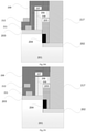
- FIG. 3 is a schematic diagram of a HHMT according to an embodiment of the present disclosure.
- the 2DEG is also formed on the other side of the channel layer.
- the HHMT 300 includes a substrate 301, a nucleation layer 304, a buffer layer 305, a channel layer 306, a channel supply layer 307, an second spacing layer 302, and a spacing layer 303, etc.
- the first electrode 333 and the second electrode 330 in ohmic contact with 2DHG 308 and the third electrode 332 in Schottky contact with channel supply layer 307 are formed on one side of the channel supply layer 307.
- the structures similar to the HHMT shown in FIG. 1 will not be repeated here.
- the HHMT is formed on the left of channel layer 306.
- the preparation process of the structure shown in Fig. 3 may be simpler.
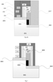
- FIG.4 is a schematic diagram of a HHMT according to an embodiment of the present disclosure.
- the substrate may be GaN intrinsic substrate.
- the structure and manufacturing process are relatively simple.
- the HHMT 400 includes a substrate 401 and a vertical interface formed on the substrate 401, resulting in a step-shape substrate structure.
- the HHMT 400 comprises a channel layer 406 and a channel supply layer 407.
- the channel layer 406 is outside of the vertical interface of substrate 401.
- the channel supply layer 407 is formed outside of the channel layer 406 and covers the channel layer 406.
- 2DHG 409 and 2DEG 408 are formed near the interface of the channel supply layer 407.
- the first electrode 411 and the second electrode 413 in ohmic contact with the 2DHG are formed on the channel supply layer 407, and the third electrode 412 is formed on the channel supply layer 407 and is in Schottky contact with the channel supply layer 407.
- the substrate material may also be SiC or sapphire Al 2 O 3 .
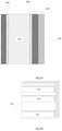
- FIG.5A is a top view of a vertical configuration of the electrodes of a HHMT according to an embodiment of the present disclosure
- FIG.5B is a solid view of a vertical configuration of the electrodes of a HHMT according to an embodiment of the present disclosure.
- HHMT 500 includes: a channel layer 501, a channel supply layer 502, a 2DEG 503, a 2DHG 504, a first electrode 505, a second electrode 506 and a third electrode 507.
- the first electrode 505, the second electrode 506 and the third electrode 507 are arranged vertically, while only the second electrode 506 can be seen in FIG.5A . This arrangement is advantageous to reduce the wafer area occupied.
- FIG.6A is a top view of a HHMT and FIG.6B is a solid view of the HHMT according to an embodiment of the present disclosure.
- the HHMT 600 includes a channel layer 601, a channel supply layer 602, a 2DEG 603, a 2DHG 604, a first electrode 605, a second electrode 606, and a third electrode 607.
- the embodiments in FIG.6A and FIG.6B show that the first electrode 605, the second electrode 606 and the third electrode 607 are arranged laterally and have the same horizontal height.
- HHMT HHMT
- the HHMT also have a variety of other structures or modifications, changes, or variants on these structures to provide different properties or functions. These structures and their improvement, alteration or variation may also be applied to the scheme of the disclosure under the technical conception of the disclosure.
- FIGs. 7A-7C shows other structures of the one-side HHMT.
- FIG.7A is a schematic diagram of a one-side HHMT according to an embodiment of the present disclosure.
- the HHMT 700 comprises a substrate 701, a channel layer 702, and a channel supply layer 703.
- the channel supply layer 703 in the left part is removed.
- the top surface of the channel layer 702 may retain a part of the channel supply layer.
- an insulating layer 707 may be introduced to cover the channel layer 702.
- FIG.7B is a schematic diagram of a one-side HHMT according to an embodiment of the present disclosure.
- the HHMT 720 comprises a substrate 701, a channel layer 702, and a channel supply layer 703.
- the insulating layer 708 is grown, and then the insulating layer 708 on the right side of channel layer 702 is etched, and the channel supply layer 703 is then grown. That is, after the channel layer is generated, an insulating layer is used to protect the channel layer, and then the channel supply layer is grown.
- 2DHG 704 exists on the left side, resulting in a HHMT having 2DHG on one side.
- FIG.7C is a schematic diagram of a HHMT according to an embodiment of the present disclosure.
- the HHMT 720 comprises a substrate 701, a spacing layer 702, a screening layer 703, the nucleation layer 703, a buffer layer 704, a channel layer 706, a channel supply layer 707, a first electrode 711, a second electrode 713, and a third electrode 712.
- a right-high-left-low stepped structure is formed on the substrate before the nucleation layer 703 grows. Meanwhile, a recess structure is included in the high-low stepped structure. Then, an insulating layer is grown and a part of the insulating layer adjacent to the vertical interface within the recess is etched off to expose the vertical interface of the substrate. Then, the nucleation 703, the buffer layer 704, the channel layer 706 and channel supply layer 707 are respective grown. Thus, only 2DHG 708 on the left exists, resulting in a HHMT having 2DHG on one side. Similarly, if the left-high-right-low stepped structure including the recess structure therein is formed and then the channel layer 706 and channel supply layer 703 are grown, a one-side 2DEG HEMT can also obtained.
- FIG.7D is a schematic diagram of a HHMT according to an embodiment of the present disclosure.
- the HHMT 720 comprises a substrate 701, a spacing layer 702, a screening layer 703, a channel layer 706, a channel supply layer 707, a first electrode 711, a second electrode 713, and a third electrode 712.
- a third electrode 706 is formed above the channel layer, but part of the channel layer 706 is still exposed. Then, the channel layer 706 continues to grow on exposed channel layer 706, covering part of the third electrode 712. The channel supply layer 707 is grown, but only the left channel was reserved to obtain one-side 2DHG 704.
- the screening layer 703 is formed on the right side of channel layer 706 and channel supply layer 707, resulting in a HHMT with a third electrode 712 on the right and a first electrode and a third electrode on the left.
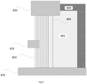
- FIG.8 is a schematic diagram of an embodiment of the present disclosure, HHMT.
- HHMT 800 includes: a channel layer 802, a channel supply layer 803, a 2DHG 804, a screening layer 809, a first electrode 835, a second electrode 830 and a third electrode 832.
- the first electrode 835 extends under the channel layer 802 and the channel supply layer 803.
- the first electrode 835 is disposed on a substrate. After completing preparation of the structure above the first electrode 835, the substrate below may still remain. In some embodiments, the substrate under the first electrode 835 may be partially or completely removed. In this way, the first electrode 835 can be lined out from the bottom to realize electrical connection.
- the second electrode 830 and the third electrode 832 are still lined out from the top to realize electrical connection.
- the high voltage of the first electrode requires a large insulation distance, which is adverse for reducing the size of the device; while in the structure shown in FIG.8 , the second electrode and the third electrode with low potential are lined out from the top of the device, and the first electrode is lined out from the bottom of the device, which can effectively save space, reduce parasitic capacitance inductance, and also facilitate subsequent device packaging.
- the structure shown in FIG.8 reduces the thermal resistance of the device by removing the silicon substrate. The heat can be effectively derived from both sides, especially the first electrode which can be directly connected to the thermal conductivity device, which can greatly reduce the thermal resistance.
- the second and third electrodes can be formed first. After removing most or all of the silicon substrate to expose 2DHG 809, the first electrode 835 is then formed. In some embodiments, it is preferable to add a support structure to the wafer prior to the removal of the silicon substrate because the mechanical strength of the wafer is significantly reduced after substrate removal.
- the second electrode 830 extends laterally along top of the channel layer 806 and/or the channel supply layer 807.
- the second electrode is placed above the device to facilitate the electrical connection in the later stage, and also facilitates the isolation between the electrodes, improving the withstand voltage and reducing the dark current.
Landscapes
- Junction Field-Effect Transistors (AREA)
- Electrodes Of Semiconductors (AREA)
- Recrystallisation Techniques (AREA)
- Insulated Gate Type Field-Effect Transistor (AREA)
Applications Claiming Priority (2)
| Application Number | Priority Date | Filing Date | Title |
|---|---|---|---|
| CN201910291624 | 2019-04-12 | ||
| PCT/CN2019/109382 WO2020206959A1 (fr) | 2019-04-12 | 2019-09-30 | Transistor à haute mobilité de trous (hhmt) et son procédé de fabrication |
Publications (3)
| Publication Number | Publication Date |
|---|---|
| EP3955312A1 true EP3955312A1 (fr) | 2022-02-16 |
| EP3955312A4 EP3955312A4 (fr) | 2022-10-19 |
| EP3955312B1 EP3955312B1 (fr) | 2024-12-04 |
Family
ID=67822538
Family Applications (3)
| Application Number | Title | Priority Date | Filing Date |
|---|---|---|---|
| EP19923756.1A Active EP3955312B1 (fr) | 2019-04-12 | 2019-09-30 | Transistor à haute mobilité de trous (hhmt) et son procédé de fabrication |
| EP20786688.0A Active EP3955315B1 (fr) | 2019-04-12 | 2020-01-17 | Dispositif à semi-conducteur et son procédé de fabrication |
| EP21764555.5A Pending EP4068387A4 (fr) | 2019-04-12 | 2021-03-02 | Dispositif à semi-conducteur, son procédé de fabrication et son utilisation |
Family Applications After (2)
| Application Number | Title | Priority Date | Filing Date |
|---|---|---|---|
| EP20786688.0A Active EP3955315B1 (fr) | 2019-04-12 | 2020-01-17 | Dispositif à semi-conducteur et son procédé de fabrication |
| EP21764555.5A Pending EP4068387A4 (fr) | 2019-04-12 | 2021-03-02 | Dispositif à semi-conducteur, son procédé de fabrication et son utilisation |
Country Status (7)
| Country | Link |
|---|---|
| US (4) | US12136669B2 (fr) |
| EP (3) | EP3955312B1 (fr) |
| JP (1) | JP7497446B2 (fr) |
| KR (1) | KR102826398B1 (fr) |
| CN (8) | CN110224019B (fr) |
| TW (1) | TWI749493B (fr) |
| WO (3) | WO2020206959A1 (fr) |
Families Citing this family (21)
| Publication number | Priority date | Publication date | Assignee | Title |
|---|---|---|---|---|
| CN110224019B (zh) * | 2019-04-12 | 2023-12-01 | 广东致能科技有限公司 | 一种半导体器件及其制造方法 |
| US12464756B2 (en) * | 2019-04-12 | 2025-11-04 | Guangdong Zhineng Technologies, Co. Ltd. | High electron mobility transistor (HEMT) and method of manufacturing the same |
| CN111816701B (zh) * | 2019-04-12 | 2024-12-27 | 广东致能科技有限公司 | 一种半导体器件及其制造方法 |
| CN113140628B (zh) * | 2020-01-17 | 2023-09-29 | 广东致能科技有限公司 | 一种半导体器件及其制造方法 |
| KR102769350B1 (ko) * | 2020-04-13 | 2025-02-14 | 광동 즈넝 테크놀로지 컴퍼니 리미티드 | 정공 채널 반도체 트랜지스터, 제조 방법 및 그 응용 |
| WO2021208623A1 (fr) * | 2020-04-13 | 2021-10-21 | 广东致能科技有限公司 | Dispositif à semi-conducteur en forme d'ailette, son procédé de fabrication et son utilisation |
| CN113571515B (zh) * | 2020-04-29 | 2024-04-09 | 广东致能科技有限公司 | 一种驱动电路、驱动ic以及驱动系统 |
| CN113571516B (zh) * | 2020-04-29 | 2024-02-06 | 广东致能科技有限公司 | 一种iii族氮化物半导体集成电路结构、制造方法及其应用 |
| CN113838929B (zh) * | 2020-06-23 | 2025-10-17 | 广东致能半导体有限公司 | 一种半导体器件及其制造方法 |
| CN113948582B (zh) * | 2020-07-15 | 2024-07-02 | 广东致能科技有限公司 | 一种二极管及其制造方法 |
| WO2022171168A1 (fr) * | 2021-02-10 | 2022-08-18 | 广东致能科技有限公司 | Filtre en volume |
| CN113921609A (zh) * | 2021-09-27 | 2022-01-11 | 深圳大学 | 一种垂直氮化镓场效应晶体管及其制备方法 |
| US12243936B2 (en) * | 2021-12-28 | 2025-03-04 | Raytheon Company | AIN channel heterostructure field effect transistor |
| CN117198877A (zh) * | 2022-05-30 | 2023-12-08 | 联华电子股份有限公司 | 高电子迁移率晶体管及其制作方法 |
| CN118281055A (zh) * | 2022-12-29 | 2024-07-02 | 广东致能科技有限公司 | 一种半导体器件及制造方法 |
| CN118281059A (zh) * | 2022-12-29 | 2024-07-02 | 广东致能科技有限公司 | 一种半导体器件及制造方法 |
| CN116031289A (zh) * | 2023-01-17 | 2023-04-28 | 湖北九峰山实验室 | 半导体射频器件及其制备方法 |
| CN116072531B (zh) * | 2023-03-07 | 2023-08-22 | 徐州致能半导体有限公司 | 一种在半导体功能区侧面制作电极的方法 |
| CN116344612B (zh) * | 2023-05-24 | 2023-08-04 | 湖北九峰山实验室 | 垂直功率器件及其制作方法 |
| CN116978943B (zh) * | 2023-09-14 | 2024-01-30 | 广东致能科技有限公司 | 一种增强型半导体器件及其制备方法 |
| CN116960175B (zh) * | 2023-09-19 | 2023-12-12 | 广东致能科技有限公司 | 一种准垂直型半导体器件及其制备方法 |
Family Cites Families (57)
| Publication number | Priority date | Publication date | Assignee | Title |
|---|---|---|---|---|
| US6265289B1 (en) * | 1998-06-10 | 2001-07-24 | North Carolina State University | Methods of fabricating gallium nitride semiconductor layers by lateral growth from sidewalls into trenches, and gallium nitride semiconductor structures fabricated thereby |
| US6177688B1 (en) * | 1998-11-24 | 2001-01-23 | North Carolina State University | Pendeoepitaxial gallium nitride semiconductor layers on silcon carbide substrates |
| JP3679720B2 (ja) * | 2001-02-27 | 2005-08-03 | 三洋電機株式会社 | 窒化物系半導体素子および窒化物系半導体の形成方法 |
| US7382001B2 (en) * | 2004-01-23 | 2008-06-03 | International Rectifier Corporation | Enhancement mode III-nitride FET |
| US8188513B2 (en) * | 2007-10-04 | 2012-05-29 | Stc.Unm | Nanowire and larger GaN based HEMTS |
| DE102007052202B3 (de) * | 2007-10-30 | 2008-11-13 | Infineon Technologies Austria Ag | Halbleiterbauelement und Verfahren zur Herstellung desselben |
| GB2482308A (en) * | 2010-07-28 | 2012-02-01 | Univ Sheffield | Super junction silicon devices |
| US8692319B2 (en) * | 2011-06-03 | 2014-04-08 | Infineon Technologies Austria Ag | Lateral trench MESFET |
| US8541293B2 (en) * | 2011-09-21 | 2013-09-24 | Institute of Microelectronics, Academy of Sciences | Method of controlled lateral etching |
| KR20160134872A (ko) * | 2011-12-19 | 2016-11-23 | 인텔 코포레이션 | 비평면 iii-n 트랜지스터 |
| KR20140013618A (ko) * | 2012-07-25 | 2014-02-05 | 엘지전자 주식회사 | 질화물 반도체 소자 및 이의 제조 방법 |
| DE102012217073B4 (de) * | 2012-09-21 | 2024-11-28 | Robert Bosch Gmbh | Vertikales mikroelektronisches Bauelement |
| KR101922123B1 (ko) * | 2012-09-28 | 2018-11-26 | 삼성전자주식회사 | 반도체소자 및 그 제조방법 |
| TWI496285B (zh) * | 2012-12-07 | 2015-08-11 | 立錡科技股份有限公司 | 高電子遷移率電晶體及其製造方法 |
| US8768271B1 (en) * | 2012-12-19 | 2014-07-01 | Intel Corporation | Group III-N transistors on nanoscale template structures |
| JP6064628B2 (ja) * | 2013-01-29 | 2017-01-25 | 富士通株式会社 | 半導体装置 |
| EP2765611A3 (fr) * | 2013-02-12 | 2014-12-03 | Seoul Semiconductor Co., Ltd. | Transistors verticaux en nitrure de gallium et leurs procédés de fabrication |
| WO2014144993A1 (fr) * | 2013-03-15 | 2014-09-18 | Ostendo Technologies, Inc. | Matrice de pixels active ayant des performances améliorées et procédé de croissance épitaxiale permettant d'obtenir cette matrice |
| US9006791B2 (en) * | 2013-03-15 | 2015-04-14 | The Government Of The United States Of America, As Represented By The Secretary Of The Navy | III-nitride P-channel field effect transistor with hole carriers in the channel |
| US20150079738A1 (en) * | 2013-06-18 | 2015-03-19 | Stephen P. Barlow | Method for producing trench high electron mobility devices |
| CN103531615A (zh) * | 2013-10-15 | 2014-01-22 | 苏州晶湛半导体有限公司 | 氮化物功率晶体管及其制造方法 |
| JP2015099903A (ja) * | 2013-10-17 | 2015-05-28 | ローム株式会社 | 窒化物半導体装置およびその製造方法 |
| WO2015059854A1 (fr) * | 2013-10-25 | 2015-04-30 | パナソニックIpマネジメント株式会社 | Appareil de pilotage de gâchette |
| KR101940234B1 (ko) * | 2013-12-03 | 2019-01-21 | 한국전자통신연구원 | 쇼트키 다이오드 및 그의 제조방법 |
| US9660064B2 (en) * | 2013-12-26 | 2017-05-23 | Intel Corporation | Low sheet resistance GaN channel on Si substrates using InAlN and AlGaN bi-layer capping stack |
| US10229991B2 (en) * | 2014-09-25 | 2019-03-12 | Intel Corporation | III-N epitaxial device structures on free standing silicon mesas |
| DE102014119465B3 (de) * | 2014-12-22 | 2016-05-25 | Infineon Technologies Ag | Halbleitervorrichtung mit streifenförmigen trenchgatestrukturen, transistormesas und diodenmesas |
| CN105280725B (zh) * | 2015-04-17 | 2019-03-12 | 苏州捷芯威半导体有限公司 | 一种氮化镓二极管及其制作方法 |
| CN107660310B (zh) * | 2015-06-26 | 2022-03-08 | 英特尔公司 | 异质外延n型晶体管与p型晶体管的基于阱的集成 |
| CN105140270B (zh) * | 2015-07-29 | 2018-01-09 | 电子科技大学 | 一种增强型hemt器件 |
| CN106611781A (zh) * | 2015-10-27 | 2017-05-03 | 上海新昇半导体科技有限公司 | 量子阱器件及其形成方法 |
| KR101774824B1 (ko) | 2015-11-09 | 2017-09-05 | 가천대학교 산학협력단 | 실리콘 나노와이어에 게르마늄 채널을 갖는 트랜지스터 및 그 제조방법 |
| US9659942B1 (en) * | 2015-11-24 | 2017-05-23 | International Business Machines Corporation | Selective epitaxy growth for semiconductor devices with fin field-effect transistors (FinFET) |
| CN105448977A (zh) | 2015-12-31 | 2016-03-30 | 深圳市华讯方舟微电子科技有限公司 | 高电子迁移率晶体管及其制造方法 |
| US11018253B2 (en) * | 2016-01-07 | 2021-05-25 | Lawrence Livermore National Security, Llc | Three dimensional vertically structured electronic devices |
| CN105679823B (zh) * | 2016-02-17 | 2019-09-03 | 香港商莫斯飞特半导体有限公司 | 一种纵向型氮化镓基异质结半导体器件及其制造方法 |
| GB2547661A (en) * | 2016-02-24 | 2017-08-30 | Jiang Quanzhong | Layered vertical field effect transistor and methods of fabrication |
| CN105762078B (zh) * | 2016-05-06 | 2018-11-16 | 西安电子科技大学 | GaN基纳米沟道高电子迁移率晶体管及制作方法 |
| KR101843917B1 (ko) * | 2016-09-06 | 2018-03-30 | 한국과학기술연구원 | 스핀-궤도 결합의 차이를 이용한 상보성 논리 소자 및 그 제조 방법 |
| CN107958934A (zh) * | 2016-10-18 | 2018-04-24 | 联华电子股份有限公司 | 不对称鳍状结构及其制作方法 |
| GB2556899B (en) * | 2016-11-24 | 2020-09-16 | Cambridge Entpr Ltd | A gallium nitride transistor |
| JP6866619B2 (ja) * | 2016-12-01 | 2021-04-28 | 日産自動車株式会社 | 半導体装置 |
| CN106410045B (zh) | 2016-12-08 | 2019-07-05 | 西安电子科技大学 | 基于CH3NH3PbI3材料的P型HHMT晶体管及其制备方法 |
| WO2018103646A1 (fr) | 2016-12-08 | 2018-06-14 | 西安电子科技大学 | Procédé à base de matériau de ch3nh3pbi3 pour fabriquer un dispositif de transistor hemt/hhmt |
| CN106549038B (zh) * | 2016-12-09 | 2019-08-02 | 宁波海特创电控有限公司 | 一种垂直结构的氮化镓异质结hemt |
| CN106684143A (zh) * | 2017-02-17 | 2017-05-17 | 杭州电子科技大学 | 基于垂直沟道的异质结场效应管器件及其制备方法 |
| US9978872B1 (en) * | 2017-03-23 | 2018-05-22 | International Business Machines Corporation | Non-polar, III-nitride semiconductor fin field-effect transistor |
| WO2018181237A1 (fr) * | 2017-03-31 | 2018-10-04 | パナソニックIpマネジメント株式会社 | Dispositif semiconducteur |
| US10658370B2 (en) * | 2017-06-29 | 2020-05-19 | Taiwan Semiconductor Manufacturing Co., Ltd. | Semiconductor device and manufacturing method thereof |
| CN109285880A (zh) * | 2017-07-19 | 2019-01-29 | 吴绍飞 | 增强型鳍式绝缘栅高电子迁移率晶体管 |
| CN109524460B (zh) | 2017-09-19 | 2022-05-17 | 世界先进积体电路股份有限公司 | 高空穴移动率晶体管 |
| WO2019066916A1 (fr) * | 2017-09-29 | 2019-04-04 | Intel Corporation | Transistors au nitrure du groupe iii de type complémentaire à jonctions de polarisation complémentaires |
| CN108511513B (zh) * | 2018-02-09 | 2019-12-10 | 海迪科(南通)光电科技有限公司 | 一种具有垂直结构的AlGaN\GaN功率器件及其制备方法 |
| WO2019188767A1 (fr) * | 2018-03-29 | 2019-10-03 | パナソニックIpマネジメント株式会社 | Dispositif à semi-conducteurs et son procédé de fabrication |
| JP7021063B2 (ja) * | 2018-12-10 | 2022-02-16 | 株式会社東芝 | 半導体装置 |
| CN110224019B (zh) * | 2019-04-12 | 2023-12-01 | 广东致能科技有限公司 | 一种半导体器件及其制造方法 |
| US11367787B2 (en) * | 2019-11-12 | 2022-06-21 | Winbond Electronics Corp. | Semiconductor device and manufacturing method thereof |
-
2019
- 2019-04-16 CN CN201910301888.5A patent/CN110224019B/zh active Active
- 2019-04-16 CN CN202311438430.7A patent/CN117334738A/zh active Pending
- 2019-04-16 CN CN202311438775.2A patent/CN117317001A/zh active Pending
- 2019-08-05 CN CN201910718112.3A patent/CN110400848B/zh active Active
- 2019-09-30 EP EP19923756.1A patent/EP3955312B1/fr active Active
- 2019-09-30 WO PCT/CN2019/109382 patent/WO2020206959A1/fr not_active Ceased
- 2019-09-30 US US17/603,297 patent/US12136669B2/en active Active
-
2020
- 2020-01-17 WO PCT/CN2020/072766 patent/WO2020207098A1/fr not_active Ceased
- 2020-01-17 EP EP20786688.0A patent/EP3955315B1/fr active Active
- 2020-01-17 US US17/603,298 patent/US12302598B2/en active Active
- 2020-03-05 CN CN202010149409.5A patent/CN111816700B/zh active Active
- 2020-03-06 US US16/811,898 patent/US11830940B2/en active Active
- 2020-03-26 TW TW109110142A patent/TWI749493B/zh active
- 2020-04-13 CN CN202010288959.5A patent/CN111816706B/zh active Active
- 2020-04-13 CN CN202010288958.0A patent/CN111816702B/zh active Active
- 2020-04-13 CN CN202411185387.2A patent/CN119050152A/zh active Pending
-
2021
- 2021-03-02 US US17/788,030 patent/US12432958B2/en active Active
- 2021-03-02 WO PCT/CN2021/078736 patent/WO2021175222A1/fr not_active Ceased
- 2021-03-02 JP JP2022549769A patent/JP7497446B2/ja active Active
- 2021-03-02 EP EP21764555.5A patent/EP4068387A4/fr active Pending
- 2021-03-02 KR KR1020227030710A patent/KR102826398B1/ko active Active
Also Published As
Similar Documents
| Publication | Publication Date | Title |
|---|---|---|
| EP3955312B1 (fr) | Transistor à haute mobilité de trous (hhmt) et son procédé de fabrication | |
| US8890239B2 (en) | Semiconductor device and method for producing the same | |
| EP3955313B1 (fr) | Transistor à haute mobilité d'électrons (hemt) et son procédé de fabrication | |
| US8941174B2 (en) | Semiconductor device and method for producing the same | |
| US12040356B2 (en) | Fin-shaped semiconductor device, fabrication method, and application thereof | |
| US20080142845A1 (en) | HEMT including MIS structure | |
| KR102769350B1 (ko) | 정공 채널 반도체 트랜지스터, 제조 방법 및 그 응용 | |
| US20230335631A1 (en) | Semiconductor device and manufacturing method therefor | |
| TWI898374B (zh) | 半導體器件及製造方法 | |
| CN222928735U (zh) | 耗尽型与增强型GaN单片集成器件 | |
| TW202427571A (zh) | 半導體器件及製造方法 | |
| CN116960174A (zh) | 一种p沟道半导体器件及其制备方法 | |
| CN118281080A (zh) | 一种肖特基二极管及制造方法 |
Legal Events
| Date | Code | Title | Description |
|---|---|---|---|
| STAA | Information on the status of an ep patent application or granted ep patent |
Free format text: STATUS: THE INTERNATIONAL PUBLICATION HAS BEEN MADE |
|
| PUAI | Public reference made under article 153(3) epc to a published international application that has entered the european phase |
Free format text: ORIGINAL CODE: 0009012 |
|
| STAA | Information on the status of an ep patent application or granted ep patent |
Free format text: STATUS: REQUEST FOR EXAMINATION WAS MADE |
|
| 17P | Request for examination filed |
Effective date: 20211108 |
|
| AK | Designated contracting states |
Kind code of ref document: A1 Designated state(s): AL AT BE BG CH CY CZ DE DK EE ES FI FR GB GR HR HU IE IS IT LI LT LU LV MC MK MT NL NO PL PT RO RS SE SI SK SM TR |
|
| DAV | Request for validation of the european patent (deleted) | ||
| DAX | Request for extension of the european patent (deleted) | ||
| REG | Reference to a national code |
Ref country code: DE Ref legal event code: R079 Ipc: H01L0029778000 Ref country code: DE Ref legal event code: R079 Ref document number: 602019063223 Country of ref document: DE Free format text: PREVIOUS MAIN CLASS: H01L0029775000 Ipc: H01L0029778000 |
|
| A4 | Supplementary search report drawn up and despatched |
Effective date: 20220921 |
|
| RIC1 | Information provided on ipc code assigned before grant |
Ipc: H01L 29/04 20060101ALN20220915BHEP Ipc: H01L 29/06 20060101ALN20220915BHEP Ipc: H01L 29/20 20060101ALN20220915BHEP Ipc: H01L 29/423 20060101ALN20220915BHEP Ipc: H01L 29/417 20060101ALN20220915BHEP Ipc: H01L 21/336 20060101ALI20220915BHEP Ipc: H01L 29/778 20060101AFI20220915BHEP |
|
| STAA | Information on the status of an ep patent application or granted ep patent |
Free format text: STATUS: EXAMINATION IS IN PROGRESS |
|
| 17Q | First examination report despatched |
Effective date: 20230630 |
|
| GRAP | Despatch of communication of intention to grant a patent |
Free format text: ORIGINAL CODE: EPIDOSNIGR1 |
|
| STAA | Information on the status of an ep patent application or granted ep patent |
Free format text: STATUS: GRANT OF PATENT IS INTENDED |
|
| RIC1 | Information provided on ipc code assigned before grant |
Ipc: H01L 29/04 20060101ALN20240606BHEP Ipc: H01L 29/06 20060101ALN20240606BHEP Ipc: H01L 29/20 20060101ALN20240606BHEP Ipc: H01L 29/423 20060101ALN20240606BHEP Ipc: H01L 29/417 20060101ALN20240606BHEP Ipc: H01L 21/336 20060101ALI20240606BHEP Ipc: H01L 29/778 20060101AFI20240606BHEP |
|
| RIC1 | Information provided on ipc code assigned before grant |
Ipc: H01L 29/04 20060101ALN20240607BHEP Ipc: H01L 29/06 20060101ALN20240607BHEP Ipc: H01L 29/20 20060101ALN20240607BHEP Ipc: H01L 29/423 20060101ALN20240607BHEP Ipc: H01L 29/417 20060101ALN20240607BHEP Ipc: H01L 21/336 20060101ALI20240607BHEP Ipc: H01L 29/778 20060101AFI20240607BHEP |
|
| INTG | Intention to grant announced |
Effective date: 20240628 |
|
| GRAS | Grant fee paid |
Free format text: ORIGINAL CODE: EPIDOSNIGR3 |
|
| GRAA | (expected) grant |
Free format text: ORIGINAL CODE: 0009210 |
|
| STAA | Information on the status of an ep patent application or granted ep patent |
Free format text: STATUS: THE PATENT HAS BEEN GRANTED |
|
| REG | Reference to a national code |
Ref country code: DE Ref legal event code: R079 Ref document number: 602019063223 Country of ref document: DE Free format text: PREVIOUS MAIN CLASS: H01L0029778000 Ipc: H10D0030470000 |
|
| AK | Designated contracting states |
Kind code of ref document: B1 Designated state(s): AL AT BE BG CH CY CZ DE DK EE ES FI FR GB GR HR HU IE IS IT LI LT LU LV MC MK MT NL NO PL PT RO RS SE SI SK SM TR |
|
| REG | Reference to a national code |
Ref country code: CH Ref legal event code: EP |
|
| P01 | Opt-out of the competence of the unified patent court (upc) registered |
Free format text: CASE NUMBER: APP_60598/2024 Effective date: 20241112 |
|
| REG | Reference to a national code |
Ref country code: DE Ref legal event code: R096 Ref document number: 602019063223 Country of ref document: DE |
|
| REG | Reference to a national code |
Ref country code: IE Ref legal event code: FG4D |
|
| REG | Reference to a national code |
Ref country code: LT Ref legal event code: MG9D |
|
| REG | Reference to a national code |
Ref country code: NL Ref legal event code: MP Effective date: 20241204 |
|
| PG25 | Lapsed in a contracting state [announced via postgrant information from national office to epo] |
Ref country code: HR Free format text: LAPSE BECAUSE OF FAILURE TO SUBMIT A TRANSLATION OF THE DESCRIPTION OR TO PAY THE FEE WITHIN THE PRESCRIBED TIME-LIMIT Effective date: 20241204 |
|
| PG25 | Lapsed in a contracting state [announced via postgrant information from national office to epo] |
Ref country code: FI Free format text: LAPSE BECAUSE OF FAILURE TO SUBMIT A TRANSLATION OF THE DESCRIPTION OR TO PAY THE FEE WITHIN THE PRESCRIBED TIME-LIMIT Effective date: 20241204 |
|
| PG25 | Lapsed in a contracting state [announced via postgrant information from national office to epo] |
Ref country code: BG Free format text: LAPSE BECAUSE OF FAILURE TO SUBMIT A TRANSLATION OF THE DESCRIPTION OR TO PAY THE FEE WITHIN THE PRESCRIBED TIME-LIMIT Effective date: 20241204 |
|
| PG25 | Lapsed in a contracting state [announced via postgrant information from national office to epo] |
Ref country code: ES Free format text: LAPSE BECAUSE OF FAILURE TO SUBMIT A TRANSLATION OF THE DESCRIPTION OR TO PAY THE FEE WITHIN THE PRESCRIBED TIME-LIMIT Effective date: 20241204 |
|
| PG25 | Lapsed in a contracting state [announced via postgrant information from national office to epo] |
Ref country code: NO Free format text: LAPSE BECAUSE OF FAILURE TO SUBMIT A TRANSLATION OF THE DESCRIPTION OR TO PAY THE FEE WITHIN THE PRESCRIBED TIME-LIMIT Effective date: 20250304 |
|
| PG25 | Lapsed in a contracting state [announced via postgrant information from national office to epo] |
Ref country code: GR Free format text: LAPSE BECAUSE OF FAILURE TO SUBMIT A TRANSLATION OF THE DESCRIPTION OR TO PAY THE FEE WITHIN THE PRESCRIBED TIME-LIMIT Effective date: 20250305 Ref country code: LV Free format text: LAPSE BECAUSE OF FAILURE TO SUBMIT A TRANSLATION OF THE DESCRIPTION OR TO PAY THE FEE WITHIN THE PRESCRIBED TIME-LIMIT Effective date: 20241204 |
|
| PG25 | Lapsed in a contracting state [announced via postgrant information from national office to epo] |
Ref country code: RS Free format text: LAPSE BECAUSE OF FAILURE TO SUBMIT A TRANSLATION OF THE DESCRIPTION OR TO PAY THE FEE WITHIN THE PRESCRIBED TIME-LIMIT Effective date: 20250304 |
|
| PG25 | Lapsed in a contracting state [announced via postgrant information from national office to epo] |
Ref country code: NL Free format text: LAPSE BECAUSE OF FAILURE TO SUBMIT A TRANSLATION OF THE DESCRIPTION OR TO PAY THE FEE WITHIN THE PRESCRIBED TIME-LIMIT Effective date: 20241204 |
|
| REG | Reference to a national code |
Ref country code: AT Ref legal event code: MK05 Ref document number: 1749134 Country of ref document: AT Kind code of ref document: T Effective date: 20241204 |
|
| PG25 | Lapsed in a contracting state [announced via postgrant information from national office to epo] |
Ref country code: SM Free format text: LAPSE BECAUSE OF FAILURE TO SUBMIT A TRANSLATION OF THE DESCRIPTION OR TO PAY THE FEE WITHIN THE PRESCRIBED TIME-LIMIT Effective date: 20241204 |
|
| PG25 | Lapsed in a contracting state [announced via postgrant information from national office to epo] |
Ref country code: PL Free format text: LAPSE BECAUSE OF FAILURE TO SUBMIT A TRANSLATION OF THE DESCRIPTION OR TO PAY THE FEE WITHIN THE PRESCRIBED TIME-LIMIT Effective date: 20241204 |
|
| PG25 | Lapsed in a contracting state [announced via postgrant information from national office to epo] |
Ref country code: IS Free format text: LAPSE BECAUSE OF FAILURE TO SUBMIT A TRANSLATION OF THE DESCRIPTION OR TO PAY THE FEE WITHIN THE PRESCRIBED TIME-LIMIT Effective date: 20250404 |
|
| PG25 | Lapsed in a contracting state [announced via postgrant information from national office to epo] |
Ref country code: PT Free format text: LAPSE BECAUSE OF FAILURE TO SUBMIT A TRANSLATION OF THE DESCRIPTION OR TO PAY THE FEE WITHIN THE PRESCRIBED TIME-LIMIT Effective date: 20250404 |
|
| PG25 | Lapsed in a contracting state [announced via postgrant information from national office to epo] |
Ref country code: EE Free format text: LAPSE BECAUSE OF FAILURE TO SUBMIT A TRANSLATION OF THE DESCRIPTION OR TO PAY THE FEE WITHIN THE PRESCRIBED TIME-LIMIT Effective date: 20241204 |
|
| PG25 | Lapsed in a contracting state [announced via postgrant information from national office to epo] |
Ref country code: AT Free format text: LAPSE BECAUSE OF FAILURE TO SUBMIT A TRANSLATION OF THE DESCRIPTION OR TO PAY THE FEE WITHIN THE PRESCRIBED TIME-LIMIT Effective date: 20241204 Ref country code: RO Free format text: LAPSE BECAUSE OF FAILURE TO SUBMIT A TRANSLATION OF THE DESCRIPTION OR TO PAY THE FEE WITHIN THE PRESCRIBED TIME-LIMIT Effective date: 20241204 |
|
| PG25 | Lapsed in a contracting state [announced via postgrant information from national office to epo] |
Ref country code: SK Free format text: LAPSE BECAUSE OF FAILURE TO SUBMIT A TRANSLATION OF THE DESCRIPTION OR TO PAY THE FEE WITHIN THE PRESCRIBED TIME-LIMIT Effective date: 20241204 |
|
| PG25 | Lapsed in a contracting state [announced via postgrant information from national office to epo] |
Ref country code: CZ Free format text: LAPSE BECAUSE OF FAILURE TO SUBMIT A TRANSLATION OF THE DESCRIPTION OR TO PAY THE FEE WITHIN THE PRESCRIBED TIME-LIMIT Effective date: 20241204 |
|
| PG25 | Lapsed in a contracting state [announced via postgrant information from national office to epo] |
Ref country code: IT Free format text: LAPSE BECAUSE OF FAILURE TO SUBMIT A TRANSLATION OF THE DESCRIPTION OR TO PAY THE FEE WITHIN THE PRESCRIBED TIME-LIMIT Effective date: 20241204 |
|
| REG | Reference to a national code |
Ref country code: DE Ref legal event code: R097 Ref document number: 602019063223 Country of ref document: DE |
|
| PG25 | Lapsed in a contracting state [announced via postgrant information from national office to epo] |
Ref country code: SE Free format text: LAPSE BECAUSE OF FAILURE TO SUBMIT A TRANSLATION OF THE DESCRIPTION OR TO PAY THE FEE WITHIN THE PRESCRIBED TIME-LIMIT Effective date: 20241204 |
|
| PG25 | Lapsed in a contracting state [announced via postgrant information from national office to epo] |
Ref country code: DK Free format text: LAPSE BECAUSE OF FAILURE TO SUBMIT A TRANSLATION OF THE DESCRIPTION OR TO PAY THE FEE WITHIN THE PRESCRIBED TIME-LIMIT Effective date: 20241204 |
|
| PGFP | Annual fee paid to national office [announced via postgrant information from national office to epo] |
Ref country code: DE Payment date: 20250919 Year of fee payment: 7 |
|
| PLBE | No opposition filed within time limit |
Free format text: ORIGINAL CODE: 0009261 |
|
| STAA | Information on the status of an ep patent application or granted ep patent |
Free format text: STATUS: NO OPPOSITION FILED WITHIN TIME LIMIT |
|
| 26N | No opposition filed |
Effective date: 20250905 |