EP3961710A1 - Dispositif d'affichage et son procédé de fabrication - Google Patents
Dispositif d'affichage et son procédé de fabrication Download PDFInfo
- Publication number
- EP3961710A1 EP3961710A1 EP20795724.2A EP20795724A EP3961710A1 EP 3961710 A1 EP3961710 A1 EP 3961710A1 EP 20795724 A EP20795724 A EP 20795724A EP 3961710 A1 EP3961710 A1 EP 3961710A1
- Authority
- EP
- European Patent Office
- Prior art keywords
- electrode
- light emitting
- emitting elements
- layer
- insulating layer
- Prior art date
- Legal status (The legal status is an assumption and is not a legal conclusion. Google has not performed a legal analysis and makes no representation as to the accuracy of the status listed.)
- Pending
Links
Images




















Classifications
-
- H—ELECTRICITY
- H10—SEMICONDUCTOR DEVICES; ELECTRIC SOLID-STATE DEVICES NOT OTHERWISE PROVIDED FOR
- H10H—INORGANIC LIGHT-EMITTING SEMICONDUCTOR DEVICES HAVING POTENTIAL BARRIERS
- H10H29/00—Integrated devices, or assemblies of multiple devices, comprising at least one light-emitting semiconductor element covered by group H10H20/00
- H10H29/10—Integrated devices comprising at least one light-emitting semiconductor component covered by group H10H20/00
- H10H29/14—Integrated devices comprising at least one light-emitting semiconductor component covered by group H10H20/00 comprising multiple light-emitting semiconductor components
- H10H29/142—Two-dimensional arrangements, e.g. asymmetric LED layout
-
- H—ELECTRICITY
- H10—SEMICONDUCTOR DEVICES; ELECTRIC SOLID-STATE DEVICES NOT OTHERWISE PROVIDED FOR
- H10W—GENERIC PACKAGES, INTERCONNECTIONS, CONNECTORS OR OTHER CONSTRUCTIONAL DETAILS OF DEVICES COVERED BY CLASS H10
- H10W90/00—Package configurations
-
- H—ELECTRICITY
- H10—SEMICONDUCTOR DEVICES; ELECTRIC SOLID-STATE DEVICES NOT OTHERWISE PROVIDED FOR
- H10D—INORGANIC ELECTRIC SEMICONDUCTOR DEVICES
- H10D86/00—Integrated devices formed in or on insulating or conducting substrates, e.g. formed in silicon-on-insulator [SOI] substrates or on stainless steel or glass substrates
- H10D86/40—Integrated devices formed in or on insulating or conducting substrates, e.g. formed in silicon-on-insulator [SOI] substrates or on stainless steel or glass substrates characterised by multiple TFTs
- H10D86/481—Integrated devices formed in or on insulating or conducting substrates, e.g. formed in silicon-on-insulator [SOI] substrates or on stainless steel or glass substrates characterised by multiple TFTs integrated with passive devices, e.g. auxiliary capacitors
-
- H—ELECTRICITY
- H10—SEMICONDUCTOR DEVICES; ELECTRIC SOLID-STATE DEVICES NOT OTHERWISE PROVIDED FOR
- H10D—INORGANIC ELECTRIC SEMICONDUCTOR DEVICES
- H10D86/00—Integrated devices formed in or on insulating or conducting substrates, e.g. formed in silicon-on-insulator [SOI] substrates or on stainless steel or glass substrates
- H10D86/40—Integrated devices formed in or on insulating or conducting substrates, e.g. formed in silicon-on-insulator [SOI] substrates or on stainless steel or glass substrates characterised by multiple TFTs
- H10D86/60—Integrated devices formed in or on insulating or conducting substrates, e.g. formed in silicon-on-insulator [SOI] substrates or on stainless steel or glass substrates characterised by multiple TFTs wherein the TFTs are in active matrices
-
- H—ELECTRICITY
- H10—SEMICONDUCTOR DEVICES; ELECTRIC SOLID-STATE DEVICES NOT OTHERWISE PROVIDED FOR
- H10H—INORGANIC LIGHT-EMITTING SEMICONDUCTOR DEVICES HAVING POTENTIAL BARRIERS
- H10H20/00—Individual inorganic light-emitting semiconductor devices having potential barriers, e.g. light-emitting diodes [LED]
- H10H20/01—Manufacture or treatment
-
- H—ELECTRICITY
- H10—SEMICONDUCTOR DEVICES; ELECTRIC SOLID-STATE DEVICES NOT OTHERWISE PROVIDED FOR
- H10H—INORGANIC LIGHT-EMITTING SEMICONDUCTOR DEVICES HAVING POTENTIAL BARRIERS
- H10H20/00—Individual inorganic light-emitting semiconductor devices having potential barriers, e.g. light-emitting diodes [LED]
- H10H20/80—Constructional details
- H10H20/81—Bodies
- H10H20/819—Bodies characterised by their shape, e.g. curved or truncated substrates
- H10H20/821—Bodies characterised by their shape, e.g. curved or truncated substrates of the light-emitting regions, e.g. non-planar junctions
-
- H—ELECTRICITY
- H10—SEMICONDUCTOR DEVICES; ELECTRIC SOLID-STATE DEVICES NOT OTHERWISE PROVIDED FOR
- H10H—INORGANIC LIGHT-EMITTING SEMICONDUCTOR DEVICES HAVING POTENTIAL BARRIERS
- H10H20/00—Individual inorganic light-emitting semiconductor devices having potential barriers, e.g. light-emitting diodes [LED]
- H10H20/80—Constructional details
- H10H20/83—Electrodes
- H10H20/831—Electrodes characterised by their shape
-
- H—ELECTRICITY
- H10—SEMICONDUCTOR DEVICES; ELECTRIC SOLID-STATE DEVICES NOT OTHERWISE PROVIDED FOR
- H10H—INORGANIC LIGHT-EMITTING SEMICONDUCTOR DEVICES HAVING POTENTIAL BARRIERS
- H10H20/00—Individual inorganic light-emitting semiconductor devices having potential barriers, e.g. light-emitting diodes [LED]
- H10H20/80—Constructional details
- H10H20/84—Coatings, e.g. passivation layers or antireflective coatings
-
- H—ELECTRICITY
- H10—SEMICONDUCTOR DEVICES; ELECTRIC SOLID-STATE DEVICES NOT OTHERWISE PROVIDED FOR
- H10H—INORGANIC LIGHT-EMITTING SEMICONDUCTOR DEVICES HAVING POTENTIAL BARRIERS
- H10H29/00—Integrated devices, or assemblies of multiple devices, comprising at least one light-emitting semiconductor element covered by group H10H20/00
- H10H29/01—Manufacture or treatment
- H10H29/036—Manufacture or treatment of packages
- H10H29/0364—Manufacture or treatment of packages of interconnections
-
- H—ELECTRICITY
- H10—SEMICONDUCTOR DEVICES; ELECTRIC SOLID-STATE DEVICES NOT OTHERWISE PROVIDED FOR
- H10H—INORGANIC LIGHT-EMITTING SEMICONDUCTOR DEVICES HAVING POTENTIAL BARRIERS
- H10H29/00—Integrated devices, or assemblies of multiple devices, comprising at least one light-emitting semiconductor element covered by group H10H20/00
- H10H29/80—Constructional details
- H10H29/85—Packages
- H10H29/8508—Package substrates, e.g. submounts
-
- H—ELECTRICITY
- H10—SEMICONDUCTOR DEVICES; ELECTRIC SOLID-STATE DEVICES NOT OTHERWISE PROVIDED FOR
- H10H—INORGANIC LIGHT-EMITTING SEMICONDUCTOR DEVICES HAVING POTENTIAL BARRIERS
- H10H29/00—Integrated devices, or assemblies of multiple devices, comprising at least one light-emitting semiconductor element covered by group H10H20/00
- H10H29/80—Constructional details
- H10H29/85—Packages
- H10H29/857—Interconnections
-
- H—ELECTRICITY
- H10—SEMICONDUCTOR DEVICES; ELECTRIC SOLID-STATE DEVICES NOT OTHERWISE PROVIDED FOR
- H10H—INORGANIC LIGHT-EMITTING SEMICONDUCTOR DEVICES HAVING POTENTIAL BARRIERS
- H10H20/00—Individual inorganic light-emitting semiconductor devices having potential barriers, e.g. light-emitting diodes [LED]
- H10H20/01—Manufacture or treatment
- H10H20/032—Manufacture or treatment of electrodes
-
- H—ELECTRICITY
- H10—SEMICONDUCTOR DEVICES; ELECTRIC SOLID-STATE DEVICES NOT OTHERWISE PROVIDED FOR
- H10H—INORGANIC LIGHT-EMITTING SEMICONDUCTOR DEVICES HAVING POTENTIAL BARRIERS
- H10H20/00—Individual inorganic light-emitting semiconductor devices having potential barriers, e.g. light-emitting diodes [LED]
- H10H20/80—Constructional details
- H10H20/81—Bodies
- H10H20/819—Bodies characterised by their shape, e.g. curved or truncated substrates
-
- H—ELECTRICITY
- H10—SEMICONDUCTOR DEVICES; ELECTRIC SOLID-STATE DEVICES NOT OTHERWISE PROVIDED FOR
- H10H—INORGANIC LIGHT-EMITTING SEMICONDUCTOR DEVICES HAVING POTENTIAL BARRIERS
- H10H20/00—Individual inorganic light-emitting semiconductor devices having potential barriers, e.g. light-emitting diodes [LED]
- H10H20/80—Constructional details
- H10H20/85—Packages
- H10H20/857—Interconnections, e.g. lead-frames, bond wires or solder balls
Definitions
- Embodiments of the present disclosure relate to a display device and a method of fabricating the same.
- a technique of manufacturing a subminiature light emitting element using a material having a reliable inorganic crystal structure and manufacturing a light emitting device using the light emitting element has been developed. For example, a technique of fabricating a plurality of subminiature light emitting elements each having a small size corresponding to a range from the nanometer scale to the micrometer scale, and forming light sources of various light emitting devices including pixels of display devices using the subminiature light emitting elements, has been developed.
- Embodiments of the present disclosure are directed to a display device having a pixel including light emitting elements, and a method of fabricating the same.
- a display device in accordance with an embodiment of the present disclosure may include a pixel disposed in a display area.
- the pixel may include: a first electrode; a first insulating layer disposed on the first electrode, and including openings formed to expose different areas of the first electrode and define respective cells; light emitting elements each disposed in the cell defined by one of the openings, and including a first end electrically connected to the first electrode, and a second end protruding upward from the first insulating layer; and a second electrode disposed over the light emitting elements, and electrically connected to the second ends of the light emitting elements.
- each of the openings may have a width less than a length of each of the light emitting elements.
- each of the light emitting elements may be arranged in a vertical direction or a diagonal direction with respect to the first electrode and the second electrode.
- the first ends of the light emitting elements may come into direct contact with the first electrode.
- the second ends of the light emitting elements may come into direct contact with the second electrode.
- each of the openings may have a polygonal shape, a circular shape, an elliptical shape, or a shape corresponding to a combination thereof, and the openings may be disposed adjacent to each other in an emission area of the pixel.
- the display device may further include first contact electrodes embedded in the respective openings, and coming into contact with the first electrode and the first ends of the light emitting elements.
- the display device may further include insulating patterns embedded in the respective openings to cover the first contact electrodes and areas of the first ends of the light emitting elements.
- the insulating patterns may include organic insulating material.
- the display device may further include a second insulating layer interposed between the first insulating layer and the second electrode and surrounding sidewalls of the light emitting elements.
- the second insulating layer may include organic insulating material, and portions of the second insulating layer may be drawn into the openings.
- the pixel further comprises at least one intermediate electrode spaced from the first electrode and the second electrode, and electrically connected between the first electrode and the second electrode via at least one light emitting element.
- the pixel may include a plurality of intermediate electrodes.
- the intermediate electrodes may be alternately disposed on a layer on which the first electrode is disposed and a layer on which the second electrode is disposed.
- the light emitting elements may include rod-type light emitting elements or core-shell light emitting elements.
- a method of fabricating a display device in accordance with an embodiment may include: forming a first electrode on a base layer; forming a first insulating layer on the first electrode; forming, on the first insulating layer, an alignment electrode overlapping the first electrode and including first openings; forming second openings overlapping the first openings in the first insulating layer, using the alignment electrode as a mask; supplying light emitting elements on the base layer, and aligning the light emitting elements in cells formed by the first and second openings by applying alignment signals to the first electrode and the alignment electrode; electrically connecting first ends of the light emitting elements to the first electrode; and forming a second electrode on second ends of the light emitting elements such that the second electrodes are electrically connected to the second ends of the light emitting elements.
- electrically connecting the first ends of the light emitting elements to the first electrode may include: forming a conductive layer covering the alignment electrode and the light emitting elements after the light emitting elements are aligned; forming an organic insulating layer on the conductive layer; and etching the conductive layer and the organic insulating layer such that the conductive layer and the organic insulating layer remain with a predetermined height or less only in the openings.
- the alignment electrode in etching the conductive layer, may be removed along therewith.
- the method may further include: forming a second insulating layer covering the first insulating layer and the light emitting elements after the alignment electrode is removed; and partially etching the second insulating layer in a thickness direction such that the second ends of the light emitting elements are exposed.
- the method may further include dividing a lower electrode pattern including the first electrode into the first electrode and at least one intermediate electrode, after the light emitting elements are aligned and before the second electrode is formed.
- forming the second electrode may include respectively forming the second electrode and at least one intermediate electrode on different light emitting elements among the light emitting elements.
- a plurality of light emitting elements may be reliably connected between a first electrode and a second electrode of each pixel, and light efficiency of each pixel may be enhanced.
- first, second, etc. may be used herein to describe various elements, these elements should not be limited by these terms. It will be further understood that the terms “comprise”, “include”, “have”, etc. when used in this specification, specify the presence of stated features, integers, steps, operations, elements, components, and/or combinations of them but do not preclude the presence or addition of one or more other features, integers, steps, operations, elements, components, and/or combinations thereof. Furthermore, when a first component or part is disposed on a second component or part, the first component or part may be not only directly on the second component or part but a third component or part may also intervene between them. Furthermore, the term “position”, “direction”, etc. used in the following description are defined in relative terms, and it should be noted that they may be changed into a reverse position or direction depending on a view angle or direction. Furthermore, a singular form may include a plural form as long as it is not specifically mentioned in a sentence.
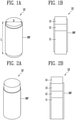
- FIGS. 1A, 1B, 2A, 2B , 3A, and 3B are perspective views and cross-sectional views each illustrating a light emitting element LD in accordance with an embodiment of the present disclosure.
- FIGS. 1A to 3B illustrate cylindrical rod-type light emitting elements LD, the type and/or shape of the light emitting elements LD in accordance with the present disclosure is not limited thereto.
- a light emitting element LD in accordance with an embodiment of the present disclosure may include a first conductivity type semiconductor layer 11, a second conductivity type semiconductor layer 13, and an active layer 12 interposed between the first and second conductivity type semiconductor layers 11 and 13.
- the light emitting element LD may include the first conductivity type semiconductor layer 11, the active layer 12, and the second conductivity type semiconductor layer 13 which are successively stacked in a longitudinal direction (L).
- the light emitting element LD may be provided in the form of a rod extending in one direction. If the direction in which the light emitting element LD extends is defined as a longitudinal direction (L), the light emitting element LD may have a first end and a second end with respect to the longitudinal direction (L).
- one of the first and second conductivity type semiconductor layers 11 and 13 may be disposed on the first end of the light emitting element LD.
- the other one of the first and second conductivity type semiconductor layers 11 and 13 may be disposed on the second end of the light emitting element LD.
- the light emitting element LD may be a rod-type light emitting element (also referred to as "rod-type light emitting diode”) fabricated in the form of a rod by an etching scheme or the like.
- rod-type embraces a rod-like shape and a bar-like shape such as a cylindrical shape and a prismatic shape extending in a longitudinal direction (i.e., to have an aspect ratio greater than 1), and the cross-sectional shape thereof is not limited to a particular shape.
- the length L of the light emitting element LD may be greater than a diameter D thereof (or a width of the cross-section thereof).
- the light emitting element LD may have a small size ranging from the nanometer scale to the micrometer scale.
- each light emitting element LD may have a diameter D (or a width) and/or a length L ranging from the nanometer scale to the micrometer scale.
- the size of the light emitting element LD is not limited thereto.
- the size of the light emitting element LD may be changed in various ways depending on design conditions of various devices, e.g., a display device, which employs, as a light source, a light emitting device using a light emitting element LD.
- the first conductivity type semiconductor layer 11 may include, for example, at least one N-type semiconductor layer.
- the first conductivity type semiconductor layer 11 may include an N-type semiconductor layer which includes any one semiconductor material of InAlGaN, GaN, AlGaN, InGaN, AlN, and InN, and is doped with a first conductive dopant such as Si, Ge, or Sn.
- a first conductive dopant such as Si, Ge, or Sn.
- the material for forming the first conductivity type semiconductor layer 11 is not limited to this, and the first conductivity type semiconductor layer 11 may be formed of various other materials.
- the active layer 12 may be disposed on the first conductivity type semiconductor layer 11 and have a single or multi-quantum well (MQW) structure.
- a cladding layer (not shown) doped with a conductive dopant may be formed over and/or under the active layer 12.
- the cladding layer may be formed of an AlGaN layer or an InAlGaN layer.
- a material such as AlGaN or AlInGaN may be used to form the active layer 12, and various other materials may be used to form the active layer 12.
- the light emitting element LD may emit light by combination of electron-hole pairs in the active layer 12. Since light emission of the light emitting element LD can be controlled based on the foregoing principle, the light emitting element LD may be used as a light source of various light emitting devices as well as a pixel of the display device.
- the second conductivity type semiconductor layer 13 may be disposed on the active layer 12 and include a semiconductor layer having a type different from that of the first conductivity type semiconductor layer 11.
- the second conductivity type semiconductor layer 13 may include at least one P-type semiconductor layer.
- the second conductivity type semiconductor layer 13 may include a P-type semiconductor layer which includes any one semiconductor material of InAlGaN, GaN, AlGaN, InGaN, AlN, and InN, and is doped with a second conductive dopant such as Mg.
- the material for forming the second conductivity type semiconductor layer 13 is not limited to this, and the second conductivity type semiconductor layer 13 may be formed of various other materials.
- the light emitting element LD may further include an insulating film INF provided on the surface of the light emitting element LD.
- the insulating film INF may be formed on the surface of the light emitting element LD to enclose an outer circumferential surface of at least the active layer 12, and may further enclose predetermined areas of the first and second conductivity type semiconductor layers 11 and 13.
- the insulating film INF may allow the opposite ends of the light emitting element LD that have different polarities to be exposed to the outside.
- the insulating film INF may expose one end of each of the first and second conductivity type semiconductor layers 11 and 13 that are disposed on the respective opposite ends of the light emitting element LD with respect to the longitudinal direction (L), e.g., may expose two base sides of the cylinder (in FIGS. 1A and 1B , the top and bottom surfaces of the light emitting element LD) rather than covering the two base sides.
- the insulating film INF may include at least one insulating material of silicon dioxide (SiO 2 ), silicon nitride (Si 3 N 4 ), aluminum oxide (Al 2 O 3 ), and titanium dioxide (TiO 2 ), but it is not limited thereto.
- the material that forms the insulating film INF is not limited to a particular material, and the insulating film INF may be formed of well-known various insulating materials.
- the light emitting element LD may further include additional other components as well as the first conductivity type semiconductor layer 11, the active layer 12, the second conductivity type semiconductor layer 13, and/or the insulating film INF.
- the light emitting element LD may further include one or more fluorescent layers, one or more active layers, one or more semiconductor layers, and/or one or more electrode layers disposed on one end of the first conductivity type semiconductor layer 11, the active layer 12, and/or the second conductivity type semiconductor layer 13.
- the light emitting element LD may further include at least one electrode layer 14 disposed on one end of the second conductivity type semiconductor layer 13.
- the light emitting element LD may further include at least one electrode layer 15 disposed on one end of the first conductivity type semiconductor layer 11.
- Each of the electrode layers 14 and 15 may be an ohmic contact electrode, but it is not limited thereto.
- Each of the electrode layers 14 and 15 may include metal or metal oxide.
- each of the electrode layers 14 and 15 may be formed of transparent electrode materials such as chromium (Cr), titanium (Ti), aluminum (Al), gold (Au), nickel (Ni), oxides or alloys thereof, indium tin oxide (ITO), indium zinc oxide (IZO), zinc oxide (ZnO), or indium tin zinc oxide (ITZO) alone or in combination.
- the electrode layers 14 and 15 may be substantially transparent or translucent. Thereby, light generated from the light emitting element LD may be emitted to the outside after passing through the electrode layers 14 and 15.
- the insulating film INF may at least partially enclose the outer circumferential surfaces of the electrode layers 14 and 15, or may not enclose the outer circumferential surfaces thereof.
- the insulating film INF may be selectively formed on the surfaces of the electrode layers 14 and 15.
- the insulating film INF may be formed to expose the opposite ends of the light emitting element LD that have different conductivity types and, for example, may expose at least one area of each of the electrode layers 14 and 15.
- the insulating film INF may not be provided.
- the active layer 12 may be prevented from short-circuiting with at least one electrode (e.g., a first or second electrode of the pixel), which is not shown. Consequently, the electrical stability of the light emitting element LD may be secured.
- the term “connecting or connection” may comprehensively refer to physical and/or electrical connecting or connection (or coupling). Furthermore, the term “connecting or connection” may comprehensively refer to direct and/or indirect connecting or connection and integral or non-integral connecting or connection.
- the insulating film INF on the surface of the light emitting element LD, occurrence of a defect on the surface of the light emitting element LD may be minimized, whereby the lifetime and efficiency of the light emitting element LD may be improved.
- the insulating film INF is formed on each light emitting element LD, even in case that a plurality of light emitting elements LD are disposed adjacent to each other, the light emitting elements LD may be prevented from undesirably short-circuiting.
- a surface treatment process may be performed to fabricate the light emitting element LD.
- each light emitting element LD may be surface-treated so that, in case that a plurality of light emitting elements LD are mixed with a fluidic solution (or solvent) and then supplied to each emission area (e.g., an emission area of each pixel), the light emitting elements LD can be evenly dispersed rather than unevenly aggregating in the solution.
- the insulating film INF itself may be formed of a hydrophobic film using hydrophobic material, or an additional hydrophobic film formed of the hydrophobic material may be formed on the insulating film INF.
- the hydrophobic material may be a material containing fluorine to exhibit hydrophobicity.
- the hydrophobic material may be applied to the light emitting elements LD in the form of a self-assembled monolayer (SAM).
- SAM self-assembled monolayer
- the hydrophobic material may include octadecyl trichlorosilane, fluoroalkyl trichlorosilane, perfluoroalkyl triethoxysilane, etc.
- the hydrophobic material may be a commercially available fluorine containing material such as Teflon TM or Cytop TM , or a corresponding material.
- a light emitting device including the light emitting element LD described above may be used not only in a display device but also in various devices which requires a light source.
- at least one subminiature light emitting element LD e.g., a plurality of subminiature light emitting elements LD each having a size ranging from the nanometer scale to the micrometer scale, may be disposed in each pixel area of the display panel to form a light source (or, a light source unit) of the corresponding pixel using the subminiature light emitting elements LD.
- the field of application of the light emitting element LD according to the present disclosure is not limited to a display device.
- the light emitting element LD may also be used in other types of devices such as a lighting device, which requires a light source.
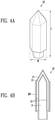
- FIGS. 4A and 4B are respectively a perspective diagram and a cross-sectional diagram illustrating a light emitting element LD in accordance with an embodiment of the present disclosure.
- FIGS. 4A and 4B illustrate a light emitting element LD having a structure different from that of the light emitting elements LD illustrated in FIGS. 1A to 3B , and for example illustrate a light emitting element having a core-shell structure.
- the type, the structure, and/or the shape of the light emitting element LD in accordance with an embodiment of the present disclosure may be changed in various ways.
- like reference numerals are used to designate components similar or equal (or corresponding) to those of the embodiments of FIGS. 1A to 3B , and detailed descriptions thereof will be omitted.
- a light emitting element LD in accordance with an embodiment of the present disclosure may include a first conductivity type semiconductor layer 11, a second conductivity type semiconductor layer 13, and an active layer 12 interposed between the first and second conductivity type semiconductor layers 11 and 13.
- the first conductivity type semiconductor layer 11 may be disposed in a central area of the light emitting element LD
- the active layer 12 may be disposed on a surface of the first conductivity type semiconductor layer 11 to enclose at least one area of the first conductivity type semiconductor layer 11.
- the second conductivity type semiconductor layer 13 may be disposed on a surface of the active layer 12 to enclose at least one area of the active layer 12.
- the light emitting element LD may further include an electrode layer 14 configured to enclose at least one area of the second conductivity type semiconductor layer 13, and/or an insulating film INF disposed on an outermost surface of the light emitting element LD.
- the light emitting element LD may further include the electrode layer 14 disposed on a surface of the second conductivity type semiconductor layer 13 to enclose one area of the second conductivity type semiconductor layer 13, and the insulating film INF disposed on a surface of the electrode layer 14 to enclose at least one area of the electrode layer 14.
- the insulating film INF may be disposed on only a portion of the surface of the light emitting element LD such that one area of the first conductivity type semiconductor layer 11 and one area of the second conductivity type semiconductor layer 13 and/or the electrode layer 14 are exposed.
- the light emitting element LD in accordance with the foregoing embodiment may be a core-shell light emitting element (also referred to as "core-shell light emitting diode”) fabricated by a growth scheme or the like.
- the light emitting element LD may have a core-shell structure including the first conductivity type semiconductor layer 11, the active layer 12, the second conductivity type semiconductor layer 13, the electrode layer 14, and the insulating film INF that are successively disposed in a direction from the center to the periphery.
- the electrode layer 14 and the insulating film INF may be selectively included in the light emitting element LD.
- the light emitting element LD may not include at least one of the electrode layer 14 and the insulating film INF.
- the light emitting element LD may have a polypyramid shape extending in one direction.
- at least one area of the light emitting element LD may have a hexagonal pyramid shape.
- the shape of the light emitting element LD may be changed in various ways.
- the light emitting element LD may have a first end and a second end with respect to the longitudinal direction (L).
- one of the first and second conductivity type semiconductor layers 11 and 13 (or an electrode layer disposed on any one side of the first and second conductivity type semiconductor layers 11 and 13) is disposed on one end of the light emitting element LD.
- the other one of the first and second conductivity type semiconductor layers 11 and 13 (or an electrode layer disposed on the other side of the first and second conductivity type semiconductor layers 11 and 13) may be disposed on the other end of the light emitting element LD.
- the light emitting element LD may be a light emitting diode, which have a core-shell structure one end of which protrudes in a polypyramid shape (e.g., a hexagonal pyramid shape), and have a subminiature size.
- the light emitting element LD may have a small size ranging from the nanometer scale to the micrometer scale, e.g., a width W and/or a length L corresponding to the nanometer scale or the micrometer scale.
- the size and the shape of the light emitting element LD may be changed depending on design conditions of various devices, e.g., a display device, which employs the light emitting element LD as a light source.
- the opposite ends of the first conductivity type semiconductor layer 11 may have shapes protruding in the longitudinal direction (L) of the light emitting element LD.
- the shapes in which the opposite ends of the first conductivity type semiconductor layer 11 protrude outward may differ from each other.
- a first end of the opposite ends of the first conductivity type semiconductor layer 11 may have a conical shape the width of which is reduced upward to form one apex.
- a second end of the opposite ends of the first conductivity type semiconductor layer 11 may have a prismatic shape (e.g., a hexagonal prism shape) having a constant width, but the present disclosure is not limited thereto.
- the first conductivity type semiconductor layer 11 may have a polygonal or stepped cross-section, the width of which is gradually reduced downward.
- the shapes of the opposite ends of the first conductivity type semiconductor layer 11 may be changed in various ways depending on embodiments, and are not limited to those of the foregoing embodiments.
- the first conductivity type semiconductor layer 11 may be disposed in a core of the light emitting element LD, i.e., a central (or middle) portion of the light emitting element LD. Furthermore, the light emitting element LD may have a shape corresponding to the shape of the first conductivity type semiconductor layer 11. For instance, if the first conductivity type semiconductor layer 11 has a hexagonal pyramid shape on at least one end thereof, the light emitting element LD may have a hexagonal pyramid shape on at least one end thereof.
- the active layer 12 may be provided and/or formed in a shape enclosing an outer circumferential surface of the first conductivity type semiconductor layer 11.
- the active layer 12 may be provided and/or formed in a shape enclosing an area of the first conductivity type semiconductor layer 11, other than one end (e.g., one end disposed at a lower position) of the first conductivity type semiconductor layer 11 with respect to the longitudinal direction (L) of the light emitting element LD.
- the second conductivity type semiconductor layer 13 may be provided and/or formed in a shape enclosing an outer circumferential surface of the active layer 12, and include a semiconductor layer having a type different from that of the first conductivity type semiconductor layer 11.
- the second conductivity type semiconductor layer 13 may have at least one P-type semiconductor layer.
- the light emitting element LD may include an electrode layer 14 that encloses an outer circumferential surface of the second conductivity type semiconductor layer 13.
- the electrode layer 14 may be an ohmic contact electrode electrically connected to the second conductivity type semiconductor layer 13, but the present disclosure is not limited thereto.
- the light emitting element LD may have a core-shell structure with the opposite ends protruding outward, and may include the first conductivity type semiconductor layer 11 provided in the central portion thereof, the active layer 12 which encloses the first conductivity type semiconductor layer 11, the second conductivity type semiconductor layer 13 which encloses the active layer 12, and the electrode layer 14 which encloses the second conductivity type semiconductor layer 13.
- the first conductivity type semiconductor layer 11 may be disposed on the first end of the light emitting element LD, and the electrode layer 14 may be disposed on the second end of the light emitting element LD.
- the light emitting element LD may further include an insulating film INF provided on the surface thereof.
- the insulating film INF may include transparent insulating material.
- the insulating film INF may be selectively provided and/or formed on the light emitting element LD.
- the insulating film INF may not be provided on the surface of the light emitting element LD.
- the insulating film INF may be provided to cover a portion of the outer circumferential surface of the first conductivity type semiconductor layer 11 and a portion of the outer circumferential surface of the electrode layer 14. In an embodiment, after the insulating film INF is first formed to cover the entirety of the outer circumferential surface of the electrode layer 14 included in the light emitting element LD, the insulating film INF may be partially removed to expose one area of the electrode layer 14 for electrical connection with an electrode, which is not shown, (e.g., a first electrode of a pixel).
- a light emitting device including the light emitting element LD described above may be used in various devices which requires a light source.
- the light emitting device may also be used in various electronic devices such as a display device or a lighting device, which requires a light source.
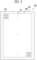
- FIG. 5 is a plan view illustrating a display device in accordance with an embodiment of the present disclosure.
- FIG. 5 illustrates a display device, particularly, a display panel PNL provided in the display device, as an example of a device which may use, as a light source, the light emitting element LD in accordance with the embodiments of FIGS. 1A to 4B .
- each pixel PXL of the display panel PNL may have at least one light emitting element LD.
- FIG. 5 simply illustrates the structure of the display panel PNL in accordance with an embodiment, focused on a display area DA.
- at least one driving circuit e.g., at least one of a scan driver and a data driver
- a plurality of lines may be further provided in the display panel PNL.
- the display panel PNL in accordance with an embodiment of the present disclosure may include a base layer BSL, and a plurality of pixels PXL disposed on the base layer BSL.
- the display panel PNL and the base layer BSL for forming the display panel PNL may include a display area DA for displaying an image, and a non-display area NDA formed in a predetermined area other than the display area DA.
- the pixels PXL may be disposed in the display area DA on the base layer BSL.
- the display area DA may be disposed in a central area of the display panel PNL, and the non-display area NDA may be disposed in a peripheral area of the display panel PNL in such a way as to enclose the display area DA.
- the locations of the display area DA and the non-display area NDA are not limited to this, and the locations thereof may be changed.
- the display area DA may form a screen on which an image is displayed.
- the base layer BSL may form a base of the display panel PNL.
- the base layer BSL may be a rigid or flexible substrate or film, and the material or properties thereof are not particularly limited.
- the base layer BSL may be a rigid substrate made of glass or reinforced glass, a flexible substrate (or a thin film) formed of plastic or metal, or at least one insulating layer, and the material and/or properties thereof are not particularly limited.
- the base layer BSL may be transparent, but the present disclosure is not limited thereto.
- the base layer BSL may be a transparent, translucent, opaque, or reflective base.
- the base layer BSL may be defined as the display area DA in which the pixels PXL are disposed, and the other area thereof may be defined as the non-display area NDA.
- the base layer BSL may include the display area DA including a plurality of pixel areas in which the respective pixels PXL are formed, and the non-display area NDA disposed around the display area DA.
- Various lines and/or internal circuits which are connected to the pixels PXL of the display area DA may be disposed in the non-display area NDA.
- the pixels PXL may be disposed in each pixel area of the display area DA.
- the pixels PXL may be arranged in the display area DA in a stripe or PenTile arrangement manner, but the present disclosure is not limited thereto.
- the pixels PXL may be arranged in the display area DA in various known arrangement manners.
- each pixel PXL may be a white pixel or a pixel configured to emit light having a specific color (e.g., red, green, or blue).
- each pixel PXL is a pixel configured to emit light of a specific color
- pixels PXL which emit light of different colors may be assembled adjacent to each other to form each pixel unit (also referred to as "unit pixel") configured to generate various colors of light.
- Each pixel PXL may include at least one light source which is driven by a predetermined control signal (e.g., a scan signal and a data signal) and/or a predetermined power source (e.g., a first power source (or first power supply) and a second power source (or second power supply)).
- a predetermined control signal e.g., a scan signal and a data signal
- a predetermined power source e.g., a first power source (or first power supply) and a second power source (or second power supply)
- each of the pixels PXL may include at least one light emitting element LD in accordance with any one of the embodiments of FIGS. 1A to 3B , e.g., at least one subminiature rod-type light emitting element LD having a small size corresponding to the nanometer scale or the micrometer scale.
- each of the pixels PXL may include at least one light emitting element LD in accordance with the embodiment of FIGS. 4A and 4B , e.g., at least one subminiature core-shell light emitting element LD having a small size corresponding to the nanometer scale or the micrometer scale.
- different types of light emitting elements LD may be used as a light source of the pixel PXL.
- each pixel PXL may be formed of an active pixel.
- the types, structures, and/or driving schemes of the pixels PXL capable of being applied to the display device according to the present disclosure are not particularly limited.
- each pixel PXL may have the same structure as that of a pixel for passive or active light emitting display devices which have various known structures and/or may be operated in various known driving schemes.
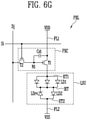
- FIGS. 6A to 6G are circuit diagrams each illustrating a pixel PXL in accordance with an embodiment of the present disclosure.
- FIGS. 6A to 6G illustrate different embodiments of the pixel PXL which can be applied to an active display device.
- the types of pixels PXL and display devices to which embodiments of the present disclosure may be applied are not limited thereto.
- each pixel PXL illustrated in FIGS. 6A to 6G may be any one of the pixels PXL provided in the display panel PNL of FIG. 5 .
- the pixels PXL may have substantially the same or similar structure.
- the pixel PXL in accordance with an embodiment of the present disclosure may include a light source unit LSU configured to generate light having a luminance corresponding to a data signal.
- the pixel PXL may selectively further include a pixel circuit PXC configured to drive the light source unit LSU.
- the light source unit LSU may include a plurality of light emitting elements LD that are connected between the first power source VDD and the second power source VSS.
- the light source unit LSU may include a first electrode ET1 (also referred to as "first pixel electrode") connected to the first power source VDD via the pixel circuit PXC and the first power line PL1, a second electrode ET2 connected to the second power source VSS through the second power line PL2, and a plurality of light emitting elements LD connected in parallel to each other in an identical direction between the first and second electrodes ET1 and ET2.
- the first electrode ET1 may be an anode electrode
- the second electrode ET2 may be a cathode electrode.
- each of the light emitting elements LD may include a P-type end connected to the first power source VDD through the first electrode ET1 and/or the pixel circuit PXC, and an N-type end connected to the second power source VSS through the second electrode ET2.
- the light emitting elements LD may be connected in parallel between the first electrode ET1 and the second electrode ET2 in a forward direction. As such, each of the light emitting elements LD connected in a forward direction between the first power source VDD and the second power source VSS may form a valid light source.
- a group of valid light sources may form the light source unit LSU of the pixel PXL.
- the first and second power sources VDD and VSS may have different potentials to make it possible for the light emitting elements LD to emit light.
- the first power source VDD may be set as a high-potential power source
- the second power source VSS may be set as a low-potential power source.
- a difference in potential between the first and second power sources VDD and VSS may be set to a threshold voltage of the light emitting elements LD or more during at least an emission period of the pixel PXL.
- the first ends (e.g., the P-type ends) of the light emitting elements LD that form each light source unit LSU may be connected in common to the pixel circuit PXC through one electrode of the light source unit LSU (e.g., the first electrode ET1 (referred also as to "first pixel electrode” or “first alignment electrode”) of each pixel PXL), and be connected to the first power source VDD through the pixel circuit PXC and the first power line PL1.
- the first electrode ET1 referred also as to "first pixel electrode” or “first alignment electrode”
- the second ends (e.g., the N-type ends) of the light emitting elements LD may be connected in common to the second power source VSS through another electrode of the light source unit LSU (e.g., a second electrode ET2 (referred also as to "second pixel electrode” or “second alignment electrode”) of each pixel PXL) and the second power line PL2.
- a second electrode ET2 referred also as to "second pixel electrode” or “second alignment electrode” of each pixel PXL
- the light emitting elements LD of the light source unit LSU may emit light having a luminance corresponding to driving current supplied thereto through the pixel circuit PXC.
- the pixel circuit PXC may supply, to the light source unit LSU, driving current corresponding to a gray scale value of data of the corresponding frame.
- the driving current supplied to the light source unit LSU may be divided into parts that flow to the light emitting elements LD connected in the forward direction.
- each of the light emitting elements LD may emit light having a luminance corresponding to current applied thereto, so that the light source unit LSU may emit light having a luminance corresponding to the driving current.
- the light source unit LSU may further include at least one invalid light source, as well as including the light emitting elements LD that form each valid light source.
- at least one reverse light emitting element LDrv may be further connected between the first and second electrodes ET1 and ET2 of the light source unit LSU.
- Each reverse light emitting element LDrv along with the light emitting elements LD that form the valid light sources, may be connected in parallel to each other between the first and second electrodes ET1 and ET2, and may be connected between the first and second electrodes ET1 and ET2 in a direction opposite to that of the light emitting elements LD.
- the N-type end of the reverse light emitting element LDrv may be connected to the first power source VDD via the first electrode ET1 and the pixel circuit PXC.
- the P-type end of the reverse light emitting element LDrv may be connected to the second power source VSS via the second electrode ET2.
- a predetermined driving voltage e.g., a forward directional driving voltage
- the reverse light emitting element LDrv remains deactivated. Hence, current substantially does not flow through the reverse light emitting element LDrv.
- the pixel circuit PXC may be connected to a scan line Si and a data line Dj of the corresponding pixel PXL.
- the pixel circuit PXC of the pixel PXL may be connected to an i-th scan line Si and a j-th data line Dj of the display area DA.
- the pixel circuit PXC may include first and second transistors T1 and T2, and a storage capacitor Cst.
- the first transistor T1 (also referred to as “driving transistor") is connected between the first power source VDD and the light source unit LSU.
- a gate electrode of the first transistor T1 is connected to a first node N1.
- the first transistor T1 may control driving current to be supplied to the light source unit LSU in response to the voltage of the first node N1.
- the second transistor T2 (also referred to as “switching transistor”) may be connected between the data line Dj and the first node N1.
- a gate electrode of the second transistor T2 is connected to the scan line Si.
- a scan signal having a gate-on voltage e.g., a low level voltage
- the second transistor T2 is turned on to electrically connect the first node N1 to the data line Dj.
- a data signal of a corresponding frame is supplied to the data line Dj.
- the data signal is transmitted to the first node N1 via the second transistor T2. Thereby, a voltage corresponding to the data signal is charged to the storage capacitor Cst.
- One electrode of the storage capacitor Cst is connected to the first power source VDD, and the other electrode thereof is connected to the first node N1.
- the storage capacitor Cst may charge a voltage corresponding to a data signal to be supplied to the first node N1 during each frame period.
- the transistors e.g., the first and second transistors T1 and T2, included in the pixel circuit PXC have been illustrated as being formed of P-type transistors, the present disclosure is not limited to this. In other words, at least one of the first and second transistors T1 and T2 may be changed to an N-type transistor.
- both the first and second transistors T1 and T2 may be formed of N-type transistors.
- the gate-on voltage of the scan signal for writing the data signal supplied to the data line Dj in each frame period to the pixel PXL may be a high level voltage (also referred to as "gate-high voltage").
- the voltage of the data signal for turning on the first transistor T1 may be a voltage having a level opposite to that of the embodiment of FIG. 6A .
- a data signal having a higher voltage may be supplied.
- an interconnection position between the pixel circuit PXC and the light source unit LSU may be changed.
- the pixel circuit PXC may be connected between the light source unit LSU and the second power source VSS, and the storage capacitor Cst may be connected between the first node N1 and the second power source VSS.
- the present disclosure is not limited thereto.
- the pixel circuit PXC may be connected between the first power source VDD and the light source unit LSU.
- the pixel PXL shown in FIG. 6B is substantially similar in configuration and operation to the pixel PXL of FIG. 6A , except that the connection positions of some circuit elements and the voltage levels of control signals (e.g., a scan signal and a data signal) are changed depending on a change in type of the transistor. Therefore, detailed description of the pixel PXL of FIG. 6B will be omitted.
- control signals e.g., a scan signal and a data signal
- the structure of the pixel circuit PXC is not limited to the embodiments shown in FIGS. 6A and 6B .
- the configuration of the pixel circuit PXC may be similar to that of embodiments illustrated in FIGS. 6C and 6D .
- the pixel circuit PXC may be formed of a well-known pixel circuit which may have various structures and/or be operated by various driving schemes.
- the pixel circuit PXC may be further connected to a control line CLi and a sensing line SENj.
- the pixel circuit PXC of the pixel PXL disposed on the i-th row and the j-th column of the display area DA may be connected to an i-th control line CLi and a j-th sensing line SENj of the display area DA.
- the pixel circuit PXC may further include a third transistor T3.
- the third transistor T3 is connected between the first transistor T1 and the sensing line SENj.
- a first electrode of the third transistor T3 may be connected to one electrode (e.g., a source electrode) of the first transistor T1 connected to the first electrode ET1, and a second electrode of the third transistor T3 may be connected to the sensing line SENj.
- a gate electrode of the third transistor T3 may be connected to the data line Dj.
- the gate electrode of the third transistor T3 is connected to the control line CLi.
- the gate electrode of the third transistor T3 may be connected to the scan line Si.
- the third transistor T3 may be turned on by a control signal having a gate-on voltage (e.g., a high level voltage) supplied to the control line CLi during a predetermined sensing period, and thus electrically connect the sensing line SENj with the first transistor T1.
- a gate-on voltage e.g., a high level voltage
- the sensing period may be a period in which characteristic information of each of the pixels PXL disposed in the display area DA (e.g., a threshold voltage, etc. of the first transistor T1) are extracted.
- the first transistor T1 may be turned on by supplying a predetermined reference voltage capable of turning on the first transistor T1 to the first node N1 through the data line Dj and the second transistor T2, or connecting each pixel PXL to a current source or the like.
- the third transistor T3 may be turned on by supplying a control signal having a gate-on voltage to the third transistor T3, so that the first transistor T1 can be connected to the sensing line SENj.
- the characteristic information of each pixel PXL that includes the threshold voltage, etc. of the first transistor T1 may be extracted through the sensing line SENj.
- the extracted characteristic information may be used to convert image data to compensate for a deviation in characteristics between the pixels PXL.
- FIG. 6C illustrates an embodiment where all of the first, second, and third transistors T1, T2, and T3 are N-type transistors, the present disclosure is not limited thereto. For example, at least one of the first, second, and third transistors T1, T2, and T3 may be changed to a P-type transistor. Furthermore, although FIG. 6C illustrates an embodiment where the light source unit LSU is connected between the pixel circuit PXC and the second power source VSS, the light source unit LSU may be connected between the first power source VDD and the pixel circuit PXC.
- the pixel circuit PXC may be connected not only to a scan line Si of a corresponding horizontal line but also to at least one another scan line (or a control line).
- the pixel circuit PXC of the pixel PXL disposed on the i-th row of the display area DA may be further connected to an i-1-th scan line Si-1 and/or an i+1-th scan line Si+1.
- the pixel circuit PXC may be connected not only to the first and second power sources VDD and VSS but also to a third power source.
- the pixel circuit PXC may also be connected to an initialization power source Vint.
- the pixel circuit PXC may include first to seventh transistors T1 to T7 and a storage capacitor Cst.
- the first transistor T1 is connected between the first power source VDD and the light source unit LSU.
- a first electrode (e.g., a source electrode) of the first transistor T1 may be connected to the first power source VDD through the fifth transistor T5 and the first power line PL1
- a second electrode (e.g., a drain electrode) of the first transistor T1 may be connected via the sixth transistor T6 to the first electrode (e.g., the first pixel electrode of the corresponding pixel PXL) of the light source unit LSU.
- a gate electrode of the first transistor T1 is connected to a first node N1.
- the first transistor T1 may control driving current to be supplied to the light source unit LSU in response to the voltage of the first node N1.
- the second transistor T2 is connected between the data line Dj and the first electrode of the first transistor T1.
- a gate electrode of the second transistor T2 is connected to the corresponding scan line Si.
- the second transistor T2 may be turned on to electrically connect the data line Dj to the first electrode of the first transistor T1.
- a data signal supplied from the data line Dj may be transmitted to the first transistor T1.
- the third transistor T3 is connected between the other electrode of the first transistor T1 and the first node N1.
- a gate electrode of the third transistor T3 is connected to the corresponding scan line Si.
- the third transistor T3 may be turned on to connect the first transistor T1 in the form of a diode.
- the fourth transistor T4 is connected between the first node N1 and the initialization power source Vint.
- a gate electrode of the fourth transistor T4 is connected to a preceding scan line, e.g., an i-1-th scan line Si-1.
- the fourth transistor T4 may be turned on so that the voltage of the initialization power source Vint may be transmitted to the first node N1.
- the voltage of the initialization power source Vint for initializing the gate voltage of the first transistor T1 may be the lowest voltage of the data signal or less.
- the fifth transistor T5 is connected between the first power source VDD and the first transistor T1.
- a gate electrode of the fifth transistor T5 is connected to a corresponding emission control line, e.g., an i-th emission control line Ei.
- the fifth transistor T5 may be turned off when an emission control signal having a gate-off voltage (e.g., a high level voltage) is supplied to the emission control line Ei, and may be turned on in other cases.
- a gate-off voltage e.g., a high level voltage
- the sixth transistor T6 is connected between the first transistor T1 and the light source unit LSU.
- a gate electrode of the sixth transistor T6 is connected to a corresponding emission control line, e.g., the i-th emission control line Ei.
- the sixth transistor T6 may be turned off when an emission control signal having a gate-off voltage is supplied to the emission control line Ei, and may be turned on in other cases.
- the seventh transistor T7 is connected between the first electrode of the light source unit LSU (e.g., the first pixel electrode ET1 of the corresponding pixel PXL) and the initialization power source Vint.
- a gate electrode of the seventh transistor T7 is connected to any one of scan lines of a subsequent stage (a subsequent horizontal pixel column), e.g., to the i+1-th scan line Si+1.
- the seventh transistor T7 may be turned on so that the voltage of the initialization power source Vint may be supplied to the first electrode of the light source unit LSU.
- the voltage of the first electrode of the light source unit LSU may be initialized.
- the control signal for controlling the operation of the seventh transistor T7 may be changed in various ways.
- the gate electrode of the seventh transistor T7 may be connected to a scan line of a corresponding horizontal line, i.e., an i-th scan line Si.
- the seventh transistor T7 may be turned on so that the voltage of the initialization power source Vint may be supplied to the first electrode of the light source unit LSU.
- the storage capacitor Cst may be connected between the first power source VDD and the first node N1.
- the storage capacitor Cst may store a voltage corresponding both to the data signal applied to the first node N1 during each frame period and to the threshold voltage of the first transistor T1.
- the transistors included in the pixel circuit PXC e.g., the first to seventh transistors T1 to T7
- the present disclosure is not limited thereto.
- at least one of the first to seventh transistors T1 to T7 may be changed to an N-type transistor.
- FIGS. 6A to 6D illustrate embodiments in which all valid light sources, i.e., light emitting elements LD, constituting each light source unit LSU are connected in parallel to each other
- the present disclosure is not limited thereto.
- the light source unit LSU of each pixel PXL may be configured to include a serial connection structure.
- components e.g., the pixel circuit PXC
- the light source unit LSU may include at least two light emitting elements connected in series to each other.
- the light source unit LSU may include a first light emitting element LD1, a second light emitting element LD2, and a third light emitting element LD3 which are connected in series in a forward direction between the first power source VDD and the second power source VSS and thus form each valid light source.
- first light emitting element LD1 a specific light emitting element among the first, second, and third light emitting elements LD1, LD2, and LD3
- the corresponding light emitting element will be referred to as "first light emitting element LD1", “second light emitting element LD2", or "third light emitting element LD3".
- light emitting element LD or "light emitting elements LD” will be used to arbitrarily designate at least one light emitting element of the first, second, and third light emitting elements LD1, LD2, and LD3 or collectively designate the first, second, and third light emitting elements LD1, LD2, and LD3.
- the P-type end of the first light emitting element LD1 may be connected to the first power source VDD through the first electrode ET1 of the light source unit LSU, etc.
- the N-type end of the first light emitting element LD1 may be connected to the P-type end of the second light emitting element LD2 through a first intermediate electrode IET1.
- the P-type end of the second light emitting element LD2 may be connected to the N-type end of the first light emitting element LD1.
- the N-type end of the second light emitting element LD2 may be connected to the P-type end of the third light emitting element LD3 through a second intermediate electrode IET2.
- the P-type end of the third light emitting element LD3 may be connected to the N-type end of the second light emitting element LD2.
- An N-type end of the third light emitting element LD3 may be connected to the second power source VSS through the second electrode ET2 of the light source unit LSU and the second power line PL2.
- the first, second, and the third light emitting elements LD1, LD2, and LD3 may be successively connected in series between the first and second electrodes ET1 and ET2 of the light source unit LSU.
- FIG. 6E there is illustrated an embodiment where the light emitting elements LD are connected to have a three-stage serial structure
- the present disclosure is not limited thereto.
- two light emitting elements LD may be connected to have a two-stage serial structure, or four or more light emitting elements LD may be connected to have a four- or more-stage serial structure.
- the voltage to be applied between the first and second electrodes ET1 and ET2 may be increased, and the amount of driving current flowing to the light source unit LSU may be reduced, compared to a light source unit LSU having a structure in which light emitting elements LD are connected in parallel. Therefore, in the case where the serial connection structure of the light emitting elements LD is used to form the light source unit LSU of each pixel PXL, panel current flowing through the display panel PNL may be reduced as the display device is driven.
- At least one serial stage may include a plurality of light emitting elements LD connected in parallel to each other.
- the light source unit LSU may be formed of a serial/parallel combination structure.
- the light source unit LSU may be configured as illustrated in the embodiment of FIG. 6F .
- At least one serial stage that forms the light source unit LSU may include a plurality of light emitting elements LD connected in parallel to each other in a forward direction.
- the light source unit LSU may include a plurality of first light emitting elements LD1 disposed in a first serial stage (also referred to as “first stage” or “first row”), at least one second light emitting element LD2 disposed in a second serial stage (also referred to as “second stage” or “second row”) subsequent to the first serial stage, and at least one third light emitting element LD3 disposed in a third serial stage (also referred to as "third stage” or “third row”) subsequent to the second serial stage.
- the light source unit LSU may include a plurality of light emitting elements LD disposed in only two serial stages, as illustrated in FIG. 6G .
- the light source unit LSU may include at least one first light emitting element LD1 disposed in a first serial stage and having a P-type end and an N-type end which are respectively connected to a first electrode ET1 and an intermediate electrode IET, and at least one second light emitting element LD2 disposed in a second serial stage and having a P-type end and an N-type end which are respectively connected to the intermediate electrode IET and a second electrode ET2.
- the number of serial stages that form the light source unit LSU may be changed in various ways.
- the light source unit LSU may include a plurality of light emitting elements LD distributed in four or more serial stages.
- the number of light emitting elements LD connected in the forward direction in each serial stage may be changed in various ways.
- the numbers of light emitting elements LD included in the pixels PXL disposed in the display area (DA of FIG. 5 ) may be identical or similar to each other.
- the light emitting elements LD may be aligned in such a way that light emitting element ink (or also referred to as "light emitting element solution") including the light emitting elements LD is controlled to be uniformly applied to an emission area of each pixel PXL, and an electric field is controlled to be applied to each pixel PXL under uniform conditions.
- the light emitting elements LD may be relatively uniformly supplied to and aligned in each pixel PXL.
- each pixel PXL may further include at least one reverse light emitting element LDrv disposed in at least one serial stage.
- at least one of a plurality of serial stages may further include at least one reverse light emitting element LDrv connected in a direction opposite to that of the light emitting elements LD.
- the driving current of the pixel PXL may flow successively via the serial stages if at least one valid light source (e.g., the first, second, and/or third light emitting elements LD1, LD2, and/or LD3) connected in the forward direction to the serial stage is disposed.
- the light source unit LSU may emit light at a luminance corresponding to the driving current.
- each light source unit LSU may include a plurality of light emitting elements LD which are connected in a forward direction between the first and second power sources VDD and VSS and form respective valid light sources.
- the connection structure between the light emitting elements LD may be changed in various ways depending on embodiments. For example, the light emitting elements LD may be connected only in series or parallel to each other, or in a series/parallel combination structure.
- the pixel PXL may include a pixel circuit PXC and/or a light source unit LSU which may have various structures.
- the structure of the pixel PXL which may be applied to the present disclosure is not limited to the embodiments illustrated in FIGS. 6A to 6G , and each pixel PXL may have various well-known structures.
- the pixel circuit PXC included in each pixel PXL may be formed of a well-known pixel circuit which may have various structures and/or be operated by various driving schemes.
- each pixel PXL may be configured in a passive light emitting display device, or the like.
- the pixel circuit PXC may be omitted, and each of the first and second electrodes ET1 and ET2 of the light source unit LSU may be directly connected to the scan line Si, the data line Dj, a power line, and/or a control line.
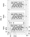
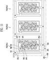
- FIG. 7 is a plan view illustrating a pixel PXL in accordance with an embodiment of the present disclosure.
- each pixel PXL illustrated in FIG. 7 may be any one of the pixels PXL illustrated in FIGS. 5 to 6G .
- each pixel PXL illustrated in FIG. 7 may be a pixel PXL including a light source unit LSU having a parallel structure, as shown in the embodiments of FIGS. 6A to 6D .
- FIG. 7 illustrates the structure of each pixel PXL, focused on the light source unit LSU.
- each pixel PXL may selectively further include circuit elements (e.g., a plurality of circuit elements that form each pixel circuit PXC) connected to the light source unit LSU.
- circuit elements e.g., a plurality of circuit elements that form each pixel circuit PXC
- FIG. 7 illustrates an embodiment in which each light source unit LSU is connected, through first and second contact holes CH1 and CH2, to a predetermined power line (e.g., first and/or second power lines PL1 and/or PL2), a circuit element (e.g., at least one circuit element that forms the pixel circuit PXC), and/or a signal line (e.g., a scan line Si and/or a data line Dj), but the present disclosure is not limited thereto.
- a predetermined power line e.g., first and/or second power lines PL1 and/or PL2
- a circuit element e.g., at least one circuit element that forms the pixel circuit PXC
- a signal line e.g., a scan line Si and/or a data line Dj
- At least one of the first and second electrodes ET1 and ET2 of each pixel PXL may be directly connected to a predetermined power line and/or signal line without using, e.g., a contact hole and/or an intermediate line.
- a plurality of pixels PXL may be regularly arranged in the display area DA.
- a first pixel PXL1 configured to emit a first color of light
- a second pixel PXL2 configured to emit a second color of light
- a third pixel PXL3 configured to emit a third color of light
- the first, second, and third pixels PXL1, PXL2, and PXL3 adjacent to each other may be assembled to form one pixel unit capable of emitting various colors of light.
- FIG. 7 illustrates an embodiment in which the first, second, and third pixels PXL1, PXL2, and PXL3 are disposed successively in the first direction DR1 (e.g., the row direction), an arrangement structure of the pixels PXL disposed in the display area DA may be changed in various ways.
- the first, second, and third pixels PXL1, PXL2, and PXL3 may be respectively a red pixel, a green pixel, and a blue pixel, but the present disclosure is not limited thereto.
- the first, second, and third pixels PXL1, PXL2, and PXL3 may include light emitting elements LD which emit different colors of light, so that the first, second, and third pixels PXL1, PXL2, and PXL3 may emit different colors of light.
- the color of light emitted from each of the first, second, and third pixels PXL1, PXL2, and PXL3 may be changed in various ways depending on embodiments.
- the first, second, and third pixels PXL1, PXL2, and PXL3 may be predetermined color pixels configured to emit an identical color of light.
- Color conversion layers and/or color filters having different colors may be disposed over the first, second, and third pixels PXL1, PXL2, and PXL3 so that different colors of light can be controlled to be emitted from the first, second, and third pixels PXL1, PXL2, and PXL3 to the outside of the display panel PNL.
- the number and/or types of pixels PXL that form each pixel unit may be changed in various ways depending on embodiments.
- the first, second, and third pixels PXL1, PXL2, and PXL3 may have a substantially identical or similar structure.
- description of a structure of each pixel PXL with reference to FIG. 7 will be focused on a structure of the first pixel PXL1.
- first pixel PXL1 first pixel PXL1
- second pixel PXL2 second pixel PXL2
- third pixel PXL3 third pixel PXL3
- pixel PXL or "pixels PXL” will be used to arbitrarily designate at least one pixel of the first, second, and the third pixels PXL1, PXL2, and PXL3 or collectively designate the first, second, and third pixels PXL1, PXL2, and PXL3.
- Each pixel PXL may include a first electrode ET1 and a second electrode ET2 each of which is disposed to overlap the corresponding emission area EMA, and a plurality of light emitting elements LD electrically connected between the first and second electrodes ET1 and ET2.
- the first and second electrodes ET1 and ET2 and the light emitting elements LD may form the light source unit LSU of each pixel PXL.
- the emission area EMA of each pixel PXL may be an area in which valid light sources, i.e., light emitting elements LD, for forming the light source unit LSU of the pixel PXL are disposed.
- the first and second electrodes ET1 and ET2 electrically connected to the light emitting elements LD may be further disposed in the emission area EMA.
- each emission area EMA may be an area enclosed by an opaque bank (also referred to as "pixel defining layer"), which is not shown.
- a mesh-shaped bank (not shown) including a plurality of openings may be formed to correspond to the emission area EMA of each pixel PXL.
- the bank may define each emission area EMA and prevent light from leaking between the pixels PXL.
- the first electrode ET1 may be a planar electrode having a shape and/or size corresponding to that of each emission area EMA.
- the present disclosure is not limited thereto.
- the first electrode ET1 may have a predetermined shape regardless of the shape of the emission area EMA.
- the first electrode ET1 may be a rectangular planar electrode having a width in the first direction DR1 (or in the second direction DR2) and a length in the second direction DR2 (or in the first direction DR1).
- the first electrode ET1 may be a plate electrode having a polygonal shape except a rectangular shape, a circular or elliptical plate electrode, or a plate electrode including a combination of boundaries of a linear line and a curved line.
- the first electrode ET1 may be a mesh type electrode including a plurality of openings. In other words, the shape and/or structure of the first electrode ET1 may be changed in various ways depending on embodiments.
- the first electrode ET1 may have a separate pattern for each of the pixels PXL.
- the first electrode ET1 may be electrically connected to a first electrode line ETL1 (also referred to as "first alignment line” or “first connection line”), and may be electrically connected to the pixel circuit PXC and/or the first power source VDD through the first electrode line ETL1 and/or the first contact hole CH1.
- the first electrode ET1 and the first electrode line ETL1 may be integrally or non-integrally connected to each other. In the case where the first electrode ET1 and the first electrode line ETL1 are integrally connected to each other, the first electrode ET1 and the first electrode line ETL1 may be regarded as being different areas of a single electrode, line, or pattern.
- the second electrode ET2 may be disposed in each emission area EMA and overlap each first electrode ET1.
- the second electrode ET2 may be disposed on a layer different from that of the corresponding first electrode ET1 at a position spaced apart from the first electrode ET1.
- the second electrode ET2 may be disposed on a layer different from that of the first electrode ET1 with the light emitting elements LD disposed in each emission area EMA interposed therebetween.
- the first electrode ET1 may be disposed under the light emitting elements LD, and the second electrode ET2 may be disposed over the light emitting elements LD.
- the second electrode ET2 may be a planar electrode having a shape and/or size corresponding to that of the corresponding first electrode ET1.
- the first and second electrodes ET1 and ET2 of each pixel PXL may have shapes and/or sizes corresponding to each other in at least the emission area EMA, and overlap each other.
- the present disclosure is not limited thereto.
- the second electrode ET2 may have a predetermined shape regardless of the shape of the emission area EMA.
- the second electrode ET2 may be a plate electrode having a polygonal shape including a rectangular shape, a circular or elliptical plate electrode, or a plate electrode including a combination of boundaries of a linear line and a curved line.
- the second electrode ET2 may be a mesh type electrode including a plurality of openings. In other words, the shape and/or structure of the second electrode ET2 may be changed in various ways depending on embodiments.
- the second electrode ET2 may be electrically connected to the second electrode line ETL2 (also referred to as "second alignment line” or “second connection line”), and may be electrically connected to the second power source VSS through the second electrode line ETL2 and/or the second contact hole CH2.
- the second electrode ET2 and the second electrode line ETL2 may be integrally or non-integrally connected to each other. In the case where the second electrode ET2 and the second electrode line ETL2 are integrally connected to each other, the second electrode ET2 and the second electrode line ETL2 may be regarded as being different areas of a single electrode, line, or pattern.
- the second electrodes ET2 of the pixels PXL may be integrally or non-integrally connected to each other.
- the second electrodes ET2 of the pixels PXL may be electrically connected to each other through the second electrode line ETL2 connected thereto.
- the first electrode line ETL1 may be connected between the first power line PL1 and the first electrode ET1.
- the first electrode line ETL1 may receive a voltage of the first power source VDD (or a first driving signal such as a scan signal, a data signal or a predetermined other control signal) supplied from the first power line PL1 during a period in which the display device is driven, and transmit the voltage of the first power source VDD to the first electrode ET1.
- the first electrode line ETL1 may be electrically connected to a first contact hole CH1, a predetermined circuit element (e.g., at least one transistor that forms the pixel circuit PXC), a power line (e.g., the first power line PL1), and/or a signal line (e.g., a scan line Si, a data line Dj, or a predetermined control line).
- a predetermined circuit element e.g., at least one transistor that forms the pixel circuit PXC
- a power line e.g., the first power line PL1
- a signal line e.g., a scan line Si, a data line Dj, or a predetermined control line.
- the first electrode line ETL1 may be electrically connected to a predetermined circuit element disposed thereunder through the first contact hole CH1, and be connected to the first power line PL1 through the circuit element.
- each pixel PXL may further include a pixel circuit PXC connected between the first electrode line ETL1 and
- the pixel circuit PXC may be disposed under each light source unit LSU and be electrically connected to the first electrode line ETL1 of the light source unit LSU through the first contact hole CH1.
- the first electrode line ETL1 may be connected, via the first contact hole CH1, etc., to a signal line to which a predetermined first driving signal is supplied.
- the first electrode line ETL1 may be directly connected to the first power line PL1 or a predetermined signal line without using the first contact hole CH1, and/or the circuit element.
- the first electrode line ETL1 may be integrally or non-integrally connected to the first power line PL1 or the predetermined signal line.
- the first electrode line ETL1 connected to the respective first electrodes ET1 of the pixels PXL may be first fabricated to be connected in common to the first electrodes ET1 of a plurality of pixels PXL, and may be supplied with a first alignment signal (or a first alignment voltage) at the step of aligning the light emitting elements LD. Thereafter, the first electrode line ETL1 between the pixels PXL may be open, so that the pixels PXL can be fabricated to be individually operable. For example, the first electrode lines ETL1 of the pixels PXL may be separated from each other between the adjacent pixels PXL.
- the second electrode line ETL2 may be connected between the second power line PL2 and the second electrode ET2.
- the second electrode line ETL2 may receive a voltage of the second power source VSS (or a second driving signal such as a scan signal, a data signal or a predetermined other control signal) during a period in which the display device is driven, and transmit the voltage of the second power source VSS to the second electrode ET2.
- the second electrode line ETL2 may be electrically connected to a second contact hole CH2, a predetermined circuit element (e.g., at least one transistor that forms the pixel circuit PXC), a power line (e.g., the second power line PL2), and/or a signal line (e.g., a scan line Si, a data line Dj, or a predetermined control line).
- a predetermined circuit element e.g., at least one transistor that forms the pixel circuit PXC
- a power line e.g., the second power line PL2
- a signal line e.g., a scan line Si, a data line Dj, or a predetermined control line.
- the second electrode line ETL2 may be connected, through the second contact hole CH2, to the second power line PL2 disposed thereunder.
- the second electrode line ETL2 may be directly connected to the second power line PL2 or a predetermined signal line without using, e.g., the second contact hole CH2, and
- the second electrode line ETL2 may be supplied with a predetermined second alignment signal (or a second alignment voltage) at the step of aligning the light emitting elements LD. During a period in which the display device is actually driven, the second electrode line ETL2 may be supplied with the voltage of the second power source VSS or a predetermined second driving signal.
- the first and second electrode lines ETL1 and ETL2 may be alignment lines which are supplied with predetermined alignment signals to be applied to each light source unit LSU at the step of aligning the light emitting elements LD in each pixel PXL to fabricate the display device and are disposed on a path along which alignment current corresponding to the alignment signal flows.
- the first and second electrode lines ETL1 and ETL2 may be connection lines which are supplied with predetermined driving voltages to be applied to each light source unit LSU at the step of driving the display device (e.g., when in use) and are disposed on a path along which driving current of each pixel PXL flows.
- a first insulating layer INS1 and the light emitting elements LD may be disposed between the first and second electrodes ET1 and ET2.
- the first insulating layer INS1 may include a plurality of openings OPN (also referred to as “through holes” or “alignment holes") which define respective cells in the emission area EMA of each pixel PXL.
- Each light emitting element LD may be disposed in any one opening OPN.
- FIG. 7 illustrates an embodiment in which only one light emitting element LD is disposed in each opening OPN, the present disclosure is not limited thereto.
- a plurality of light emitting elements LD may be disposed in at least one opening OPN, or no light emitting element LD may be disposed therein.
- the first insulating layer INS1 may be disposed on the first electrode ET1 of each pixel PXL, and include a plurality of openings OPN which expose respective different areas of the first electrode ET1 and define respective cells.
- the first insulating layer INS1 may be formed on an overall surface of the display area DA, but the present disclosure is not limited thereto.
- each first insulating layer INS1 may be individually formed in the emission area EMA of each pixel PXL.
- the first insulating layer INS1 may be formed in the form of an individual pattern provided separately for each of the pixels PXL.
- each opening OPN may be formed to have a width (or a diameter) identical with or greater than a width (or a diameter) of each light emitting element LD and less than a length of each light emitting element LD.
- each light emitting element LD may be disposed to stand vertically or diagonally in any one opening OPN such that the light emitting element LD is arranged in a vertical or diagonal direction with respect to the first and second electrodes ET1 and ET2.
- the openings OPN may have various shapes and/or arrangement structures.
- the openings OPN each may have a polygonal shape, a circular shape, an elliptical shape, or a combination thereof, and be disposed adjacent to each other in the emission area EMA of each pixel PXL.
- the openings OPN each may have a hexagonal shape, and be disposed adjacent to each other in the emission area EMA of each pixel PXL.
- the first insulating layer INS1 may have, in each emission area EMA, a honeycomb structure including a plurality of hexagonal cells defined by the openings OPN.
- At least one light emitting element LD may be disposed in at least some cells of the cells. If the openings OPN are densely disposed adjacent to each other in each emission area EMA, limited space may be more efficiently used. For example, as the openings OPN are densely disposed, space which can receive a larger number of light emitting elements LD compared to the surface area of the emission area EMA may be secured.
- Each of the light emitting elements LD may be disposed in a cell defined by any one opening OPN.
- each of the light emitting elements LD may include a first end EP1 that is electrically connected to the first electrode ET1, and a second end EP2 that protrudes upward from the first insulating layer INS1.
- the second electrode ET2 may be disposed over the light emitting elements LD. The second electrode ET2 may be electrically connected to the second ends EP2 of the light emitting elements LD that protrude upward from the first insulating layer INS1.
- each light emitting element LD may be a light emitting element having a core-shell structure.
- each light emitting element LD may be a core-shell light emitting element having a polypyramid (e.g., a hexagonal pyramid) shape.
- each light emitting element LD may include a first end EP1 disposed to face the first electrode ET1, and a second end EP2 located at a position opposite to the first end EP1 and disposed to face the second electrode ET2.
- the first end EP1 may be a P-type end
- the second end EP2 may be an N-type end, but the present disclosure is not limited thereto.
- the first end EP1 may be an N-type end
- the second end EP2 may be a P-type end.
- a plurality of openings OPN may be formed in the first insulating layer INS1, and the light emitting elements LD may be disposed to stand between the first electrode ET1 and the second electrode ET2 by using the openings OPN.
- process limitation which occurs when the light emitting elements LD are horizontally aligned may be overcome, and the light emitting elements LD may be reliably connected between the first and second electrodes ET1 and ET2.
- FIG. 8 is a cross-sectional view illustrating a pixel PXL in accordance with an embodiment of the present disclosure and for example illustrates an embodiment of a cross-section corresponding to line I-I' of FIG. 7 .
- FIG. 8 representatively illustrate only one transistor (e.g., a first transistor T1) and a storage capacitor Cst of the circuit elements disposed in each pixel area of the circuit element layer PCL.
- transistors that form each pixel circuit PXC may have a substantially identical or similar structure, but the present disclosure is not limited thereto.
- the pixel PXL in accordance with an embodiment of the present disclosure and the display device including the pixel PXL may include a display element layer DPL including a plurality of light emitting elements LD disposed in the emission area EMA of each pixel PXL.
- the pixel PXL and the display device including the pixel PXL may selectively further include at least one of a circuit element layer PCL (also referred to as "pixel circuit layer") and a cover layer CVL.
- the pixel PXL and the display device including the pixel PXL may include a circuit element layer PCL, a display element layer DPL, and a cover layer CVL which are successively disposed on one surface of the base layer BSL.
- the circuit element layer PCL and/or the cover layer CVL may be omitted.
- the circuit element layer PCL may include at least one circuit element electrically connected to the light emitting elements LD of the corresponding pixel PXL.
- the circuit element layer PCL may include at least one circuit element which forms the pixel circuit PXC of each pixel PXL.
- the circuit element layer PCL may include a plurality of transistors and a storage capacitor Cst that are disposed in each pixel area and form the corresponding pixel circuit PXC, and further include at least one power line and/or a signal line that is connected to the pixel circuit PXC and/or the light source unit LSU.
- the term "pixel area" may comprehensively refer to an area where components for constituting each pixel PXL are disposed and/or formed.
- each pixel area may include an emission area EMA where a first electrode ET1 and a second electrode ET2 that form the light source unit LSU of the corresponding pixel PXL, and a plurality of light emitting elements LD connected between the first and second electrodes ET1 and ET2 are disposed.
- Each pixel area may selectively further include a pixel circuit area where circuit elements (e.g., a plurality of transistors and at least one capacitor that form each pixel circuit PXC) that are electrically connected to the light emitting elements LD are disposed.
- circuit elements e.g., a plurality of transistors and at least one capacitor that form each pixel circuit PXC
- each pixel area may include an emission area EMA and a pixel circuit area.
- FIG. 8 representatively illustrates a transistor (e.g., the first transistor T1) connected to each first electrode ET1 and a power line (e.g., the second power line PL2) connected to each second electrode ET2, among the circuit elements and the lines that are disposed in the circuit element layer PCL.
- the planar/sectional structure of the circuit element layer PCL may be changed in various ways.
- the position and cross-sectional structure of each of the transistors including the first transistor T1 may be changed in various ways depending on embodiments.
- the circuit element layer PCL may include a plurality of insulating layers disposed between respective electrodes and/or lines.
- the circuit element layer PCL may include a buffer layer BFL, a gate insulating layer GI, an interlayer insulating layer ILD, and a passivation layer PSV which are successively stacked on one surface of the base layer BSL.
- the circuit element layer PCL may further include at least one light shielding pattern (not shown) disposed under at least some transistors.
- the buffer layer BFL may prevent impurities from diffusing into each circuit element.
- the buffer layer BFL may be formed of a single layer, or may be formed of multiple layers having at least double layers. In the case where the buffer layer BFL is formed of multiple layers, the respective layers may be formed of the same material or different materials. In an embodiment, the buffer layer BFL may be omitted.
- the first transistor T1 may include a semiconductor layer SCL, a gate electrode GE, and first and second transistor electrodes TE1 and TE2.
- FIG. 8 illustrates an embodiment in which the first transistor T1 includes the first and second transistor electrodes TE1 and TE2 that are formed separately from the semiconductor layer SCL, the present disclosure is not limited thereto.
- the first and/or second transistor electrode TE1 and/or TE2 provided in the first transistor T1 may be integrated with the corresponding semiconductor layer SCL.
- the semiconductor layer SCL may be disposed on the buffer layer BFL.
- the semiconductor layer SCL may be disposed between the gate insulating layer GI and the base layer BSL on which the buffer layer BFL is formed.
- the semiconductor layer SCL may include a first area which comes into contact with each first transistor electrode TE1, a second area which comes into contact with each second transistor electrode TE2, and a channel area disposed between the first and second areas.
- one of the first and second areas may be a source area, and the other may be a drain area.
- the semiconductor layer SCL may be a semiconductor pattern formed of polysilicon, amorphous silicon, an oxide semiconductor, etc.
- the channel area of the semiconductor layer SCL may be an intrinsic semiconductor, which is an undoped semiconductor pattern.
- Each of the first and second areas of the semiconductor layer SCL may be a semiconductor pattern doped with a predetermined impurity.
- the gate electrode GE may be disposed on the semiconductor layer SCL with the gate insulating layer GI interposed therebetween.
- the gate electrode GE may be disposed between the gate insulating layer GI and the interlayer insulating layer ILD and overlap one area of the semiconductor layer SCL.
- the first and second transistor electrodes TE1 and TE2 may be disposed on each semiconductor layer SCL with at least one interlayer insulating layer ILD interposed therebetween.
- the first and second transistor electrodes TE1 and TE2 may be disposed on respective different ends of the semiconductor layer SCL with the gate insulating layer GI and the interlayer insulating layer ILD interposed therebetween.
- the first and second transistor electrodes TE1 and TE2 may be electrically connected to each semiconductor layer SCL.
- the first and second transistor electrodes TE1 and TE2 may be connected to the first and second areas of the semiconductor layer SCL through corresponding contact holes which pass through the gate insulating layer GI and the interlayer insulating layer ILD.
- any one of the first and second transistor electrodes TE1 and TE2 may be a source electrode, and the other may be a drain electrode.
- At least one transistor provided in the pixel circuit PXC may be electrically connected to the first or second electrode ET1 or ET2 of at least one corresponding pixel PXL.
- any one (e.g., the drain electrode) of the first and second transistor electrodes TE1 and TE2 of the first transistor T1 may be electrically connected to the first electrode ET1 of the corresponding pixel PXL through the first contact hole CH1 passing through the passivation layer PSV and/or the first electrode line ETL1 provided over the passivation layer PSV.
- the storage capacitor Cst may include a first capacitor electrode CET1 and a second capacitor electrode CET2 which overlap each other.
- each of the first and second capacitor electrodes CET1 and CET2 may be formed of a single layer or multiple layers.
- at least one of the first and second capacitor electrodes CET1 and CET2 may be disposed on a layer identical with that of at least one electrode or the semiconductor layer SCL of the first transistor T1.
- the first capacitor electrode CET1 may be formed of a multilayer electrode including a lower electrode LE disposed on a layer identical with that of the semiconductor layer SCL of the first transistor T1, and an upper electrode UE disposed on a layer identical with that of the first and second transistor electrodes TE1 and TE2 of the first transistor T1 and electrically connected to the lower electrode LE.
- the second capacitor electrode CET2 may be formed of a single layer electrode which is disposed on a layer identical with that of the gate electrode of the first transistor T1 and overlaps the lower electrode LE and the upper electrode UE of the first capacitor electrode CET1.
- any one of the first and second capacitor electrodes CET1 and CET2 may include at least one layer of conductive pattern disposed on a layer different from that of the electrodes (e.g., the gate electrode GE, and the first and second transistor electrodes TE1 and TE2) and the semiconductor layer SCL that form the first transistor T1.
- At least one signal line and/or power line that is connected to each pixel PXL may be disposed on a layer identical with that of one electrode of each of the circuit elements that form the pixel circuit PXC.
- the scan line Si of each pixel PXL may be disposed on a layer identical with that of the gate electrode GE of the first transistor T1.
- the data line Dj of each pixel PXL may be disposed on a layer identical with that of the first and second transistor electrodes TE1 and TE2 of the first transistor T1.
- the first and/or second power lines PL1 and/or PL2 may be disposed on a layer identical with that of the gate electrode GE or the first and second transistor electrodes TE1 and TE2 of the first transistor T1.
- the second power line PL2 for supplying the voltage of the second power source VSS may be disposed on a layer identical with that of the gate electrodes GE of the first transistor T1, and electrically connected to the second electrode ET2 of the light source unit LSU and/or the second electrode line ETL2, both through a bridge pattern BRP disposed on a layer identical with that of the first and second transistor electrodes TE1 and TE2 of the first transistor T1 and through a second contact hole CH2 passing through at least the passivation layer PSV.
- the structures and/or positions of the second power line PL2, etc. may be changed in various ways.
- the display element layer DPL may include a light source unit LSU of each of the pixels PXL.
- the display element layer DPL may include a first electrode ET1 and a second electrode ET2 which are disposed in the emission area EMA of each pixel PXL and overlap each other, and a first insulating layer INS1 and light emitting elements LD which are disposed between the first and second electrodes ET1 and ET2.
- the display element layer DPL may further include at least one contact electrode configured to more reliably connect the light emitting elements LD to the first or second electrode ET1 or ET2.
- the display element layer DPL may further include a plurality of first contact electrodes CE1 which come into contact with the respective first ends EP1 of the light emitting elements LD and the first electrode ET1.
- the display element layer DPL may selectively further include at least one insulating layer and/or insulating pattern.
- the display element layer DPL may further include a plurality of insulating patterns INP embedded in the respective openings OPN, and at least one of a second insulating layer INS2 interposed between the first insulating layer INS1 and the second electrode ET2, and a third insulating layer INS3 disposed on the second electrode ET2 to cover the second electrode ET2.
- the first electrode ET1 may be disposed on one surface of the base layer BSL.
- the first electrode ET1 may be disposed on one surface of the base layer BSL on which the circuit element layer PCL is formed.
- the first electrode ET1 may include at least one conductive material.
- the first electrode ET1 may include at least one material among at least one metal of various metal materials including silver (Ag), magnesium (Mg), aluminum (Al), platinum (Pt), palladium (Pd), gold (Au), nickel (Ni), neodymium (Nd), iridium (Ir), chrome (Cr), titanium (Ti), molybdenum (Mo), copper (Cu), etc., or an alloy thereof, conductive oxide such as indium tin oxide (ITO), indium zinc oxide (IZO), zinc oxide (ZnO), antimony zinc oxide (AZO), indium tin zinc oxide (ITZO), tin oxide (SnO 2 ), and a conductive polymer such as PEDOT, but the present disclosure is not limited thereto.
- the first electrode ET1 may include other conductive materials including a carbon nano tube, a graphene, etc.
- the first electrode ET1 may include at least one of various conductive materials to have conductivity, and the constituent material thereof is not particularly limited.
- the first electrode ET1 may be a reflective electrode, a transparent electrode, or an opaque electrode, and the material or property thereof is not particularly limited so long as it can provide satisfactory conductivity.
- synthetically taking into account a contrast ratio, light efficiency, etc. the constituent material, structure, thickness, and/or the like of the first electrode ET1 may be determined.
- the first electrode ET1 is formed of a reflective electrode including at least one reflective electrode layer, the light output efficiency of the pixel PXL may be enhanced.
- the first electrode ET1 may be formed of a single layer or multiple layers.
- the first electrode ET1 may include a reflective electrode layer including reflective conductive material.
- the first electrode ET1 may selectively further include at least one of at least one transparent electrode layer disposed over and/or under the reflective electrode layer, and at least one conductive capping layer covering an upper portion of the reflective electrode layer and/or the transparent electrode layer.
- the reflective electrode layer of the first electrode ET1 may be formed of conductive material having a uniform reflectivity.
- the reflective electrode layer may include at least one of various metal materials including silver (Ag), magnesium (Mg), aluminum (Al), platinum (Pt), palladium (Pd), gold (Au), nickel (Ni), neodymium (Nd), iridium (Ir), chrome (Cr), titanium (Ti), molybdenum (Mo), copper (Cu), etc., or an alloy thereof., but the present disclosure is not limited thereto.
- reflective electrode layer may be formed of various reflective conductive materials. In the case where the first electrode ET1 includes the reflective electrode layer, light emitted from the light emitting elements LD may more efficiently travel in a direction (e.g., a frontal direction) in which an image is displayed.
- the transparent electrode layer of the first electrode ET1 may be formed of various transparent conductive materials.
- the transparent electrode layer may include ITO, IZO or ITZO, but the present disclosure is not limited thereto.
- the first electrode ET1 may have a triple-layer structure having a stacked structure of ITO/Ag/ITO. As such, if the first electrode ET1 is formed of multiple layers having at least two layers, voltage drop due to signal delay (RC delay) may be minimized. Thus, a desired voltage can be effectively transmitted to the light emitting elements LD.
- RC delay signal delay
- the first electrode ET1 includes a conductive capping layer covering the reflective electrode layer and/or the transparent electrode layer, it is possible to prevent the reflective electrode layer of the first electrode ET1 from being damaged due to defects caused during the process of manufacturing the pixel PXL.
- the conductive capping layer may be selectively included in the first electrode ET1, and may be omitted in some embodiments.
- the conductive capping layer may be regarded as a component of the first electrode ET1 or a separate component disposed on the first electrode ET1.
- the first insulating layer INS1 may be disposed on the first electrode ET1.
- the first insulating layer INS1 may be formed to cover a predetermined area of the first electrode ET1, and include a plurality of openings OPN which exposes other predetermined areas of the first electrode ET1.
- the openings OPN may expose different predetermined areas of the first electrode ET1 and define respective cells for receiving the corresponding light emitting elements LD.
- the first insulating layer INS1 may be formed of a single layer or multiple layers, and include at least one inorganic insulating material and/or organic insulating material.
- the first insulating layer INS1 may include various known types of inorganic insulating materials and/or organic insulating materials, and the constituent material of the first insulating layer INS1 is not particularly limited.
- the first insulating layer INS1 may include at least one organic layer.
- an upper surface of the first insulating layer INS1 may be substantially planar.
- a plurality of light emitting elements LD may be supplied to and aligned in each pixel area, particularly, the emission area EMA of each pixel PXL, in which the first insulating layer INS1 is formed.
- a plurality of light emitting elements LD may be supplied to each emission area EMA by an inkjet scheme, a slit coating scheme, or the like.
- the light emitting elements LD may be aligned in a vertical or diagonal direction in the respective openings OPN by applying predetermined alignment signals (or alignment voltages) to the first electrode ET1 and an alignment electrode (not shown) disposed on the first insulating layer INS1.
- the alignment electrode may be formed on the first insulating layer INS1 before the alignment of the light emitting elements LD, and then removed after the alignment of the light emitting elements LD are completed.
- Each of the light emitting elements LD may include a first end EP1 that is electrically connected to the first electrode ET1, and a second end EP2 that is electrically connected to the second electrode ET2.
- the first ends EP1 of the light emitting elements LD may come into direct contact with the first electrode ET1 and thus be electrically connected to the first electrode ET1.
- the present disclosure is not limited thereto.
- the first end EP1 of at least one of the light emitting elements LD may be electrically connected to the first electrode ET1 through the first contact electrode CE1 rather than coming into direct contact with the first electrode ET1.
- the second ends EP2 of the light emitting elements LD may come into direct contact with the second electrode ET2 and thus be electrically connected to the second electrode ET2.
- the present disclosure is not limited thereto.
- the second end EP2 of at least one of the light emitting elements LD may be electrically connected to the second electrode ET2 through at least one electrode (e.g., a second contact electrode, which is not shown) rather than coming into direct contact with the second electrode ET2.
- the first contact electrodes CE1 may be embedded in the respective openings OPN and be brought into contact with the first electrode ET1 of each pixel PXL and the first ends EP1 of the light emitting elements LD. If the first contact electrodes CE1 are formed, the first ends EP1 of the light emitting elements LD may be more reliably connected to the first electrode ET1.
- the first contact electrodes CE1 may include at least one conductive material identical with or different from that of the first electrode ET1, and the constituent material thereof is not particularly limited. Furthermore, each of the first contact electrodes CE1 may be formed of a single layer or multiple layers, and the structure thereof may be variously changed.
- the first contact electrodes CE1 may be formed of a transparent electrode including transparent conductive material. In this case, light emitted from the respective first ends EP1 of the light emitting elements LD may pass through the first contact electrodes CE1.
- the insulating patterns INP may be embodied in the respective openings OPN to cover respective predetermined areas of the first ends EP1 of the light emitting elements LD and the first contact electrodes CE1.
- the insulating patterns INP may be formed in the openings OPN in which the light emitting elements LD and the first contact electrodes CE1 are formed, so that the insulating patterns INP may at least partially enclose the first ends EP1 of the light emitting elements LD. If the insulating patterns INP are formed, the first ends EP1 of the light emitting elements LD may be prevented or mitigated from being damaged during a subsequent process after the alignment of the light emitting elements LD.
- each of the insulating patterns INP may include at least one organic insulating material and be formed of a single layer or multiple layers.
- each of the insulating patterns INP may include at least one organic layer.
- organic insulating material may be smoothly drawn into each of the openings OPN, so that the first ends EP1 of the light emitting elements LD may be prevented from being damaged during a subsequent process.
- the second insulating layer INS2 may be disposed between the first insulating layer INS1 and the second electrode ET2 and enclose exposed sidewalls of the light emitting elements LD. If the second insulating layer INS2 is formed, a short-circuit defect may be effectively prevented from occurring between the first electrode ET1 and the second electrode ET2, and the light emitting elements LD may be more reliably supported.
- the second insulating layer INS2 may include at least one organic insulating material and be formed of a single layer or multiple layers.
- the second insulating layer INS2 may include at least one organic layer.
- organic insulating material may be smoothly drawn into each of the openings OPN.
- a portion of the second insulating layer INS2 may be drawn into the openings OPN to enclose the light emitting elements LD and completely fill in space formed in the openings OPN. Consequently, electrical stability between the first and second electrodes ET1 and ET2 may be secured, and the light emitting elements LD may be reliably supported.
- the second electrode ET2 may be disposed on the light emitting elements LD to cover upper portions of the light emitting elements LD.
- the second electrode ET2 may be disposed on the light emitting elements LD to completely cover the second ends EP2 of the light emitting elements LD that are exposed upward from the first and second insulating layers INS1 and INS2.
- the second electrode ET2 may be electrically connected to the second power line PL2 through the bridge pattern BRP and/or the second contact hole CH2 that passes through the passivation layer PSV, the first insulating layer INS1, and the second insulating layer INS2. Therefore, the voltage of the second power source VSS may be applied to the second ends EP2 of the light emitting elements LD.
- the second electrode ET2 may include at least one conductive material.
- the second electrode ET2 may include at least one conductive material identical with or different from that of the first electrode ET1, and be formed of a single layer or multiple layers.
- the second electrode ET2 may be formed of a transparent electrode including at least one transparent conductive material so as to allow light to pass therethrough.
- the second electrode ET2 may be substantially transparent.
- substantially transparence may mean that light is allowed to be transmitted to satisfy a predetermined degree or more of transmissivity.
- the second electrode ET2 may include at least one opaque conductive material, and be formed to be substantially transparent by having a mesh structure with a plurality of holes allowing light to pass therethrough or having a very small thickness.
- the constituent material, structure, and/or thickness of the second electrode ET2 may be accordingly adjusted.
- the third insulating layer INS3 may be disposed on the second electrode ET2.
- the third insulating layer INS3 may be formed on the overall surface of the display area DA to cover the second electrodes ET2 of the pixels PXL.
- the third insulating layer INS3 may be formed of a single layer or multiple layers, and include at least one inorganic insulating material and/or organic insulating material.
- the third insulating layer INS3 may include various kinds of known organic/inorganic insulating materials including silicon nitride (SiNx), silicon oxide (SiOx), aluminum oxide (Al 2 O 3 ), etc.
- the constituent material of the third insulating layer INS3 is not particularly limited.
- the third insulating layer INS3 may include a thin-film encapsulation layer having a multilayered structure.
- the third insulating layer INS3 may be formed of a thin-film encapsulation layer having a multilayer structure including at least two inorganic insulating layers, and at least one organic insulating layer interposed between the at least two inorganic insulating layers.
- the constituent material and/or structure of the third insulating layer INS3 may be changed in various ways.
- a cover layer CVL may be selectively disposed on the third insulating layer INS3.
- the cover layer CVL may include an overcoat layer OC, a window, or the like, and further include various other functional films, etc.
- the plurality of openings OPN are formed in the first insulating layer INS1, whereby a plurality of cells for receiving the light emitting elements LD are defined.
- the light emitting elements LD may be aligned to stand vertically or diagonally between the first electrode ET1 and the second electrode ET2. In this case, process limitation which occurs in case that the light emitting elements LD are horizontally aligned may be overcome, and the light emitting elements LD may be more reliably connected between the first and second electrodes ET1 and ET2.
- the light emitting elements LD are horizontally arranged and the first and second ends EP1 and EP2 of the light emitting elements LD are thereafter connected to the first and second electrodes ET1 and ET2 through the respective contact electrodes, a separation distance for preventing reliably a short-circuit from occurring between the first and second electrodes ET1 and ET2 is required taking into account process distribution when the contact electrodes are formed.
- a reduction in length of the light emitting elements LD is limited.
- the length of the light emitting elements LD is increased, it may be difficult to uniformly disperse the light emitting elements LD in the light emitting element ink, so that it may be difficult to uniformly distribute the light emitting elements LD in each emission area EMA.
- the process limitation that occurs in case that the light emitting elements LD are horizontally arranged may be overcome, and the light emitting elements LD may be reliably connected between the first and second electrodes ET1 and ET2.
- the light efficiency (e.g., the light output rate) of each pixel PXL may be enhanced.
- the light emitting elements LD may emit light from opposite ends thereof with respect to the longitudinal direction, i.e., from the first and second ends EP1 and EP2. Therefore, if the light emitting elements LD are horizontally disposed, the light emitting elements LD emit light sideways with respect to each pixel PXL, so that the efficiency of light that is emitted in the frontal direction may be reduced.
- a separate structure such as a reflective partition wall or the like may be formed around the light emitting elements LD to guide, in the frontal direction, light emitted sideways, additional space and process may be required.
- the amount of light that is emitted in the frontal direction of each pixel PXL e.g., an image display surface of the display panel PNL
- the light efficiency of each pixel PXL may be enhanced.
- FIGS. 9A to 9M are cross-sectional views sequentially illustrating a method of fabricating a display device in accordance with an embodiment of the present disclosure and for example illustrate an embodiment of a method of fabricating a display device including the pixel PXL of FIGS. 7 and 8 .
- FIG. 10 is a plan view illustrating the pixel PXL in accordance with an embodiment of the present disclosure and, in detail, a plan view illustrating the emission area EMA of the pixel PXL immediately after the openings OPN are formed in the first insulating layer INS1, as illustrated in FIG. 9D .
- the circuit element layer PCL is formed on one surface of the base layer BSL, and the first electrode ET1 is formed on the base layer BSL on which the circuit element layer PCL is formed.
- the first electrode ET1 may be directly formed on one surface of the base layer BSL (or the base layer BSL on which the buffer layer BFL is formed).
- the first electrode ET1 may be formed through a process of forming a conductive layer including at least one conductive material and/or a patterning process, and may be formed through various types of known processes.
- the first electrode ET1 may be formed of a single layer or multiple layers.
- the first electrode ET1 may be formed of a conductive pattern having a single-layer structure, or a conductive pattern having a multilayer structure including a first reflective electrode and a first conductive capping layer.
- the first insulating layer INS1 is formed on the first electrode ET1.
- the first insulating layer INS1 may be formed on the overall surface of the display area DA including the first electrodes ET1 of the pixels PXL, or may be formed in the form of an individual pattern in the emission area EMA of each of the pixels PXL.
- the first insulating layer INS1 may be formed, e.g., by coating at least one organic insulating layer including at least one organic insulating material.
- the first insulating layer INS1 may be formed such that a surface thereof is substantially planar.
- the material and/or method of forming the first insulating layer INS1 is not limited thereto.
- the first insulating layer INS1 may be formed through a deposition process of an insulating layer including at least one inorganic insulating material and/or organic insulating material, and may be formed through various types of known processes.
- an alignment electrode ALE including a plurality of first openings OPN1 is formed on the first insulating layer INS1.
- the alignment electrode ALE may be formed through a process of forming a conductive layer including at least one conductive material and/or a patterning process, and may be formed through various types of known processes.
- the alignment electrode ALE may be formed by forming a conductive layer on the overall surface of the display area DA such that the conductive layer overlaps the first electrodes ET1 of the pixel PXL, and then patterning the conductive layer such that a plurality of first openings OPN1 are included in an area overlapping the first electrodes ET1.
- the alignment electrode ALE may overlap the first electrode ET1 of each pixel PXL and be formed to include a plurality of first openings OPN1 in an area overlapping each first electrode ET1.
- each first opening OPN1 may be formed to have a width (or a diameter) identical with or greater than a width (or a diameter) of each of the light emitting elements LD and less than a length of each of the light emitting elements LD.
- a plurality of second openings OPN2 that overlap the first openings OPN1 may be formed in the first insulating layer INS1 by etching the first insulating layer INS1 using the alignment electrode ALE as a mask.
- a pair of first opening OPN1 and second opening OPN2 that correspond to each other may form an integrated opening OPN.
- first openings OPN1 and OPN2 the corresponding openings will be referred to as “first openings OPN1” or “second openings OPN2”.
- opening OPN or “openings OPN” will be used to arbitrarily designate at least one opening of the first and second openings OPN1 and OPN2, or collectively designate the first and second openings OPN1 and OPN2.
- the second openings OPN2 may be formed in the first insulating layer INS1 through a vertical dry etching process using the alignment electrode ALE as a mask.
- the scheme of etching the first insulating layer INS1 is not limited thereto.
- the second openings OPN2 may be formed in the first insulating layer INS1 through various other etching schemes.
- a plurality of cells for receiving the light emitting elements LD may be defined by forming, in the first insulating layer INS1 and the alignment electrode ALE, a plurality of openings OPN that overlap the respective first electrodes ET1.
- the openings OPN may expose different predetermined areas of the first electrode ET1 and be disposed adjacent to each other on the first electrode ET1.
- a plurality of light emitting elements LD are supplied on the base layer BSL on which a plurality of cells are defined on each first electrode ET1.
- alignment signals may be applied to the first electrode ET1 and the alignment electrode ALE.
- an AC type alignment signal may be applied to any one electrode of the first electrode ET1 and the alignment electrode ALE, and a reference voltage having a reference potential (e.g., a ground potential) may be supplied to the other electrode. Consequently, an electric field may be formed between the first electrode ET1 and the alignment electrode ALE, and the light emitting elements LD may be aligned in at least some openings OPN.
- the light emitting elements LD may be supplied into each emission area EMA by applying the light emitting element ink with a plurality of light emitting elements LD dispersed therein onto the base layer BSL through an inkjet printing scheme, a slit coating scheme, or the like.
- the scheme of supplying the light emitting elements LD is not limited thereto, and the light emitting elements LD may be supplied onto a predetermined area of the base layer BSL in various other ways.
- each of the light emitting elements LD may be aligned to stand vertically or diagonally in any one opening OPN.
- the first ends EP1 of the light emitting elements LD may be brought into direct contact with portions of the first electrode ET1 that are exposed through the respective openings OPN, and be electrically connected to the first electrode ET1.
- the present disclosure is not limited thereto.
- the first end EP1 of at least one light emitting element LD may not completely come into contact with the first electrode ET1.
- a conductive layer CTL for covering the alignment electrode ALE and the light emitting elements LD may be formed.
- the conductive layer CTL may be formed by applying, through a sputtering scheme or the like, transparent conductive material to one surface of the base layer BSL on which the alignment electrode ALE and the light emitting elements LD are disposed.
- the material and/or scheme of forming the conductive layer CTL is not limited thereto.
- an insulating layer including organic insulating material i.e., an organic insulating layer INL
- the organic insulating layer INL may be drawn into the openings OPN and charged into the internal space of the openings OPN.
- the organic insulating layer INL may be etched such that the organic insulating layer INL remains with a predetermined height or less in only the openings OPN.
- the insulating patterns INP embedded in the respective openings OPN may be formed by etching the organic insulating layer INL by a predetermined thickness through a half ashing process.
- the organic insulating layer INL has penetrated into the openings OPN, so that, when the organic insulating layer INL is etched in the thickness direction, predetermined areas of the organic insulating layer INL that has deeply penetrated into the openings OPN may remain, and only the other areas of the organic insulating layer INL may be selectively removed.
- the predetermined areas of the organic insulating layer INL that have deeply penetrated into the openings OPN may enclose predetermined areas of the light emitting elements LD (e.g., the first ends EP1 and/or peripheral areas of the first ends EP1) rather than being removed.
- the first contact electrodes CE1 may be formed in the respective openings OPN by etching the conductive layer CTL such that the conductive layer CTL remains only in the openings OPN with a predetermined height or less.
- the alignment electrode ALE may be removed along therewith.
- the conductive layer CTL and the alignment electrode ALE may be etched and/or removed simultaneously or successively.
- the first contact electrodes CE1 may be embedded in the openings OPN such that the first contact electrodes CE1 comes into contact with the first ends EP1 of the light emitting elements LD and the first electrode ET1.
- the first contact electrodes CE1 that electrically connect the first ends EP1 of the light emitting elements LD to the first electrode ET1 may be formed through the above-mentioned process of FIGS. 9F to 9I . Hence, the first ends EP1 of the light emitting elements LD may be reliably connected to the first electrode ET1. During a process of etching the conductive layer CTL and the alignment electrode ALE, the first ends EP1 of the light emitting elements LD and/or the peripheral areas thereof may be enclosed and protected by the insulating patterns INP. Hence, the light emitting elements LD may be prevented from being damaged during a subsequent process, and the connection between the light emitting elements LD and the first electrode ET1 may be reliably maintained.
- the second insulating layer INS2 is formed on the first insulating layer INS1 and the light emitting elements LD.
- the second insulating layer INS2 may be formed to have a thickness sufficient to completely cover the first insulating layer INS1 and the light emitting elements LD.
- the second insulating layer INS2 may be partially etched in a thickness direction to expose the second ends EP2 of the light emitting elements LD, as illustrated in FIG. 9K .
- the second ends EP2 of the light emitting elements LD may be exposed by etching the second insulating layer INS2 by a predetermined distance through a half ashing process.
- a second contact hole CH2 passing through at least the second insulating layer INS2 is formed.
- the second contact hole CH2 may be formed to pass through the passivation layer PSV, the first insulating layer INS1, and the second insulating layer INS2 and expose the bridge pattern BRP.
- FIGS. 9A to 9M there is illustrated that after the second insulating layer INS2 is formed, the second contact hole CH2 passing through the passivation layer PSV, the first insulating layer INS1, and the second insulating layer INS2 is formed at a time, the present disclosure is not limited thereto.
- the passivation layer PSV, the first insulating layer INS1, and the second insulating layer INS2 may be simultaneously or successively open.
- the second insulating layer INS2 may be at least one organic insulating layer coated with organic insulating material.
- the second insulating layer INS2 may be smoothly drawn into the openings OPN during a process of forming the second insulating layer INS2. Consequently, the second insulating layer INS2 may be charged into the space formed in the openings OPN (e.g., space formed in upper areas of the openings OPN) and stably enclose the sidewalls of the light emitting elements LD.
- the first electrode ET1, the first contact electrodes CE1, etc. may be effectively prevented from short-circuiting with the second electrode ET2 to be formed during a subsequent process.
- the second electrode ET2 is formed on the light emitting elements LD so that the second electrode ET2 is electrically connected with the second ends EP2 of the light emitting elements LD.
- the second electrode ET2 may be formed on the second ends EP2 of the light emitting elements LD such that the second electrode ET2 comes into direct contact with the second ends EP2 of the light emitting elements LD that are exposed upward from the second insulating layer INS2.
- a second contact electrode (not illustrated) may be formed on the second ends EP2 of the light emitting elements LD, and the second electrode ET2 may be thereafter formed on the second contact electrode such that the second electrode ET2 is connected with the second contact electrode.
- the third insulating layer INS3 is formed on one surface of the base layer BSL on which the second electrode ET2 is formed.
- the third insulating layer INS3 may be formed in the overall area of the display area DA.
- the third insulating layer INS3 may be a thin-film encapsulation layer having at least one organic/inorganic insulating layer, but the present disclosure is not limited thereto.
- the overcoat layer OC shown in FIG. 8 , etc. may be formed on one surface of the base layer BSL on which the third insulating layer INS3 is formed.
- the cover layer CVL may be selectively further formed after the third insulating layer INS3 is formed.
- the pixel PXL according to an embodiment of the present disclosure and the display device including the pixel PXL may be fabricated.
- the pixel PXL in accordance with the embodiments of FIGS. 7 and 8 and the display panel PNL including the pixel PXL may be fabricated.
- FIG. 11 is a plan view illustrating a pixel PXL in accordance with an embodiment of the present disclosure, and for example illustrates a modification of the embodiment of FIG. 7 .
- FIG. 12 is a cross-sectional view illustrating a pixel PXL in accordance with an embodiment of the present disclosure and for example illustrates an embodiment of a cross-section corresponding to line II-II' of FIG. 11 .
- like reference numerals will be used to designate components similar or equal to those of the embodiment of FIGS. 7 and 8 , and detailed explanation thereof will be omitted.
- the light emitting elements LD may be rod-type light emitting elements.
- each light emitting element LD may be a rod-type light emitting element which includes a first conductivity type semiconductor layer 11, an active layer 12, a second semiconductor layer 13, and an electrode layer 14 which are successively stacked, as shown in FIGS. 2A and 2B and further includes an insulating film INF disposed on a surface thereof.
- the light emitting elements LD may be light emitting elements LD having various structures, shapes, and/or types.
- the light emitting elements LD may be a substantially identical type of light emitting elements, but the present disclosure is not limited thereto.
- a combination of core-shell light emitting elements LD and rod-type light emitting elements LD may form the light source unit LSU of each pixel PXL.
- the first ends EP1 of the light emitting elements LD that are disposed to face the first electrode ET1 and electrically connected to the first electrode ET1 may be P-type ends (e.g., the respective ends each on which the electrode layer 14 of FIG. 2B is formed).
- the second ends EP2 of the light emitting elements LD that are disposed to face the second electrode ET2 and electrically connected to the second electrode ET2 may be N-type ends (e.g., the respective ends each on which the first conductivity type semiconductor layer 11 of FIG. 2B is formed).
- this may be changed depending on the connection position of the light source unit LSU and/or the connection direction of the light emitting elements LD.
- FIGS. 13A to 13I are cross-sectional views sequentially illustrating a method of fabricating a display device in accordance with an embodiment of the present disclosure and for example illustrate an embodiment of a method of fabricating a display device including the pixel PXL of FIGS. 11 and 12 .
- FIGS. 13A to 13I respectively correspond to FIGS. 9E to 9L .
- like reference numerals are used to designate components similar or equal to those of the foregoing embodiment (e.g., the embodiments of FIGS. 9A to 9M ), and detailed explanation thereof will be omitted.
- the process before supplying the light emitting elements LD may be substantially identical with that of the foregoing embodiment.
- the first electrode ET1 may be formed on one surface of the base layer BSL on which the circuit element layer PCL is formed, and the first insulating layer INS1 and the alignment electrode ALE each of which includes a plurality of openings OPN may be formed on the first electrode ET1.
- each of the light emitting elements LD may be a rod-type light emitting element which includes a first end EP1 that comes into contact with the first electrode ET1, and a second end EP2 that faces the first end EP1.
- the conductive layer CTL and the organic insulating layer INL may be successively formed to cover the alignment electrode ALE and the light emitting elements LD.
- the first contact electrodes CE1 and the insulating patterns INP may be formed by selectively etching the conductive layer CTL and the organic insulating layer INL.
- the alignment electrode ALE is removed.
- the second insulating layer INS2 is partially etched in the thickness direction such that the second ends EP2 of the light emitting elements LD are exposed.
- the second electrode ET2 is formed on the light emitting elements LD such that the second electrode ET2 is electrically connected with the second ends EP2 of the light emitting elements LD.
- the third insulating layer INS3 is formed on one surface of the base layer BSL on which the second electrode ET2 is formed.
- the overcoat layer OC shown in FIG. 12 , etc. may be formed on one surface of the base layer BSL on which the third insulating layer INS3 is formed.
- the cover layer CVL may be selectively further formed after the third insulating layer INS3 is formed.
- the pixel PXL according to an embodiment of the present disclosure and the display device including the pixel PXL may be fabricated.
- the pixel PXL in accordance with the embodiments of FIGS. 11 and 12 and the display panel PNL including the pixel PXL may be fabricated.
- the method of fabricating the display device in accordance with the embodiments of FIGS. 13A to 13I may be substantially identical with the method of fabricating the display device in accordance with the embodiments of FIGS. 9A to 9M , except the type and/or shape of the light emitting elements LD. Therefore, detailed descriptions pertaining to this will be omitted.
- FIG. 14 is a plan view illustrating a pixel PXL in accordance with an embodiment of the present disclosure, and for example illustrates a modification of the embodiment of FIG. 11 .
- FIG. 15 is a cross-sectional view illustrating a pixel PXL in accordance with an embodiment of the present disclosure and for example illustrates an embodiment of a cross-section corresponding to line III-III' of FIG. 14 .
- FIGS. 14 and 15 illustrate the pixel PXL that forms a light source unit LSU using rod-type light emitting elements LD, as shown in the embodiments of FIGS. 11 and 12 , the type of light emitting elements LD in accordance with the present disclosure is not limited thereto.
- rod-type light emitting elements LD in accordance with the present embodiment may be replaced with core-shell light emitting elements LD disclosed in the embodiments of FIGS. 7 and 8 .
- like reference numerals will be used to designate components similar or equal to those of the previous embodiments, and detailed explanation thereof will be omitted.
- each pixel PXL may further include at least one intermediate electrode which is spaced apart from the first electrode ET1 and the second electrode ET2 and electrically connected between the first and second electrodes ET1 and ET2 via at least one light emitting element LD.
- the pixel PXL may include a plurality of intermediate electrodes which are alternately disposed on a layer on which the first electrode ET1 is disposed, and a layer on which the second electrode ET2 is disposed.
- the pixel PXL may include first to fourth intermediate electrodes IET1 to IET4 which are successively connected between the first electrode ET1 and the second electrode ET2.
- the first intermediate electrode IET1 along with the second electrode ET2 may be disposed on the second insulating layer INS2, and be disposed to partially overlap the first electrode ET1.
- the first intermediate electrode IET1 may be electrically connected to the first electrode ET1 through at least one light emitting element LD.
- the at least one light emitting element LD may be connected in a forward direction between the first electrode ET1 and the first intermediate electrode IET1.
- the at least one light emitting element LD may include a first end EP1 and a second end EP2 which are respectively connected to the first electrode ET1 and the first intermediate electrode IET1.
- the first end EP1 and the second end EP2 may be respectively a P-type end and an N-type end.
- each light emitting element LD of which the P-type end is connected to the first electrode ET1 and of which the N-type end is connected to the first intermediate electrode IET1 may form a valid light source of a corresponding serial stage (e.g., the first serial stage).
- the second intermediate electrode IET2 along with the first electrode ET1 may be disposed on the passivation layer PSV, and be disposed to partially overlap the first intermediate electrode IET1.
- the second intermediate electrode IET2 may be electrically connected to the first intermediate electrode IET1 through at least one light emitting element LD.
- the at least one light emitting element LD may be connected in the forward direction between the first intermediate electrode IET1 and the second intermediate electrode IET2.
- the at least one light emitting element LD may include a second end EP2' and a first end EP1' which are respectively connected to the first intermediate electrode IET1 and the second intermediate electrode IET2.
- the second end EP2' and the first end EP1' may be respectively a P-type end and an N-type end.
- each light emitting element LD of which the P-type end is connected to the first intermediate electrode IET1 and of which the N-type end is connected to the second intermediate electrode IET2 may form a valid light source of a corresponding serial stage (e.g., the second serial stage).
- the third intermediate electrode IET3 along with the second electrode ET2 may be disposed on the second insulating layer INS2, and be disposed to partially overlap the second intermediate electrode IET2.
- the third intermediate electrode IET3 may be electrically connected to the second intermediate electrode IET2 through at least one light emitting element LD.
- the at least one light emitting element LD may be connected in the forward direction between the second intermediate electrode IET2 and the third intermediate electrode IET3.
- the at least one light emitting element LD may include a first end EP1 and a second end EP2 which are respectively connected to the second intermediate electrode IET2 and the third intermediate electrode IET3.
- the first end EP1 and the second end EP2 may be respectively a P-type end and an N-type end.
- each light emitting element LD of which the P-type end is connected to the second intermediate electrode IET2 and of which the N-type end is connected to the third intermediate electrode IET3 may form a valid light source of a corresponding serial stage (e.g., the third serial stage).
- the fourth intermediate electrode IET4 along with the first electrode ET1 may be disposed on the passivation layer PSV, and be disposed to partially overlap the third intermediate electrode IET3.
- the fourth intermediate electrode IET4 may be electrically connected to the third intermediate electrode IET3 through at least one light emitting element LD.
- the at least one light emitting element LD may be connected in the forward direction between the third intermediate electrode IET3 and the fourth intermediate electrode IET4.
- the at least one light emitting element LD may include a second end EP2' and a first end EP1' which are respectively connected to the third intermediate electrode IET3 and the fourth intermediate electrode IET4.
- the second end EP2' and the first end EP1' may be respectively a P-type end and an N-type end.
- each light emitting element LD of which the P-type end is connected to the third intermediate electrode IET3 and of which the N-type end is connected to the fourth intermediate electrode IET4 may form a valid light source of a corresponding serial stage (e.g., the fourth serial stage).
- the fourth intermediate electrode IET4 may also be disposed to partially overlap the second electrode ET2.
- the fourth intermediate electrode IET4 may be electrically connected to the second electrode ET2 through at least one light emitting element LD.
- the at least one light emitting element LD may be connected in the forward direction between the fourth intermediate electrode IET4 and the second electrode ET2.
- the at least one light emitting element LD may include a first end EP1 and a second end EP2 which are respectively connected to the fourth intermediate electrode IET4 and the second electrode ET2.
- the first end EP1 and the second end EP2 may be respectively a P-type end and an N-type end.
- each light emitting element LD of which the P-type end is connected to the fourth intermediate electrode IET4 and of which the N-type end is connected to the second electrode ET2 may form a valid light source of a corresponding serial stage (e.g., the fifth serial stage).
- each of the first to fourth intermediate electrodes IET1 to IET4 may be electrically connected to the first electrode ET1 or the second electrode ET2 and supplied with a predetermined alignment signal, at the step of aligning the light emitting elements LD. After the alignment of the light emitting elements LD are completed, each of the first to fourth intermediate electrodes IET1 to IET4 may be separated in the form of an individual electrode. In an embodiment, an area between the first electrode ET1 and at least one intermediate electrode disposed on a layer identical with the first electrode ET1 may be filled with insulating material drawn thereinto during a process of depositing the insulating pattern INP and/or the second insulating layer INS2 after an electrode separation process. For example, the insulating pattern INP and/or the second insulating layer INS2 may be interposed between the first electrode ET1, the second intermediate electrode IET2, and the fourth intermediate electrode IET4.
- a plurality of light emitting elements LD for forming each light source unit LSU may be connected in a serial/parallel combination structure.
- FIGS. 16A to 16E are cross-sectional views sequentially illustrating a method of fabricating a display device in accordance with an embodiment of the present disclosure and for example illustrate an embodiment of a method of fabricating a display device including the pixel PXL of FIGS. 14 and 15 .
- like reference numerals will be used to designate components similar or equal to those of the previous embodiments, and detailed explanation thereof will be omitted.
- a process before supplying the light emitting elements LD may be substantially identical or similar to that of the embodiment described with reference to FIGS. 9A to 9D .
- a lower electrode pattern ETP including the first electrode ET1 and at least one intermediate electrode may be formed on one surface of the base layer BSL on which the circuit element layer PCL is formed.
- the lower electrode pattern ETP that integrally includes the first electrode ET1, the second intermediate electrode IET2, and the fourth intermediate electrode IET4 may be formed on one surface of the base layer BSL.
- the first insulating layer INS1 and the alignment electrode ALE each of which includes a plurality of openings OPN may be formed on the lower electrode pattern ETP.
- the alignment electrode ALE, the first insulating layer INS1, and the lower electrode pattern ETP may be patterned in an area corresponding to space between the first electrode ET1, the second intermediate electrode IET2, and the fourth intermediate electrode IET4 through various patterning processes including a photo process.
- the alignment electrode ALE, the first insulating layer INS1, and the lower electrode pattern ETP may be simultaneously or successively patterned. Thereby, the lower electrode pattern ETP may be divided into the first electrode ET1, the second intermediate electrode IET2, and the fourth intermediate electrode IET4.
- the conductive layer CTL is removed between the first electrode ET1, the second intermediate electrode IET2, and the fourth intermediate electrode IET4.
- the first electrode ET1, the second intermediate electrode IET2, and the fourth intermediate electrode IET4 may be prevented from short-circuiting with each other.
- the first contact electrodes CE1 and the insulating patterns INP are formed by forming the organic insulating layer INL on the conductive layer CTL, and selectively etching the conductive layer CTL and the organic insulating layer INL.
- organic insulating material may be drawn between the first electrode ET1, the second intermediate electrode IET2, and the fourth intermediate electrode IET4, so that the insulating pattern INP may also be formed therebetween.
- the second insulating layer INS2 is formed to completely cover the first insulating layer INS1 and the light emitting elements LD, the second insulating layer INS2 is partially etched in the thickness direction such that the second ends EP2 and EP2' of the light emitting elements LD are exposed.
- At least one intermediate electrode and the second electrode ET2 are formed on some different light emitting elements LD of the light emitting elements LD.
- the first intermediate electrode IET1, the third intermediate electrode IET3, and the second electrode ET2 may be respectively formed on some different light emitting elements LD of the light emitting elements LD.
- the third insulating layer INS3 and/or the overcoat layer OC may be formed, whereby the display panel PNL including the pixel PXL in accordance with the embodiment of FIGS. 14 and 15 may be fabricated.
- FIGS. 17A to 17D are cross-sectional views sequentially illustrating a method of fabricating a display device in accordance with an embodiment of the present disclosure and for example illustrate an embodiment of a method of fabricating a display device including the pixel PXL of FIGS. 14 and 15 .
- like reference numerals will be used to designate components similar or equal to those of the previous embodiments, and detailed explanation thereof will be omitted.
- the first insulating layer INS1 and the lower electrode pattern ETP are successively patterned, whereby the lower electrode pattern ETP may be divided into the first electrode ET1, the second intermediate electrode IET2, and the fourth intermediate electrode IET4.
- the second insulating layer INS2 is formed, and the first intermediate electrode IET1, the third intermediate electrode IET3, and the second electrode ET2 are formed on the second insulating layer INS2.
- organic insulating material is drawn into space between the first electrode ET1, the second intermediate electrode IET2, and the fourth intermediate electrode IET4, so that a predetermined area of the second insulating layer INS2 may also be disposed therebetween.
- the step of performing the process of separating the lower electrode pattern ETP may be changed in various ways depending on embodiments.
Landscapes
- Electroluminescent Light Sources (AREA)
- Devices For Indicating Variable Information By Combining Individual Elements (AREA)
Applications Claiming Priority (2)
| Application Number | Priority Date | Filing Date | Title |
|---|---|---|---|
| KR1020190047876A KR20200124799A (ko) | 2019-04-24 | 2019-04-24 | 표시 장치 및 그의 제조 방법 |
| PCT/KR2020/000814 WO2020218713A1 (fr) | 2019-04-24 | 2020-01-16 | Dispositif d'affichage et son procédé de fabrication |
Publications (2)
| Publication Number | Publication Date |
|---|---|
| EP3961710A1 true EP3961710A1 (fr) | 2022-03-02 |
| EP3961710A4 EP3961710A4 (fr) | 2023-01-11 |
Family
ID=72941620
Family Applications (1)
| Application Number | Title | Priority Date | Filing Date |
|---|---|---|---|
| EP20795724.2A Pending EP3961710A4 (fr) | 2019-04-24 | 2020-01-16 | Dispositif d'affichage et son procédé de fabrication |
Country Status (5)
| Country | Link |
|---|---|
| US (1) | US12224307B2 (fr) |
| EP (1) | EP3961710A4 (fr) |
| KR (2) | KR20200124799A (fr) |
| CN (1) | CN113785400B (fr) |
| WO (1) | WO2020218713A1 (fr) |
Cited By (1)
| Publication number | Priority date | Publication date | Assignee | Title |
|---|---|---|---|---|
| EP4443504A1 (fr) * | 2023-03-29 | 2024-10-09 | Samsung Display Co., Ltd. | Dispositif d'affichage et procédé de fabrication de dispositif d'affichage |
Families Citing this family (13)
| Publication number | Priority date | Publication date | Assignee | Title |
|---|---|---|---|---|
| KR20200124799A (ko) * | 2019-04-24 | 2020-11-04 | 삼성디스플레이 주식회사 | 표시 장치 및 그의 제조 방법 |
| KR102794236B1 (ko) * | 2019-10-15 | 2025-04-15 | 삼성디스플레이 주식회사 | 표시 장치의 제조 방법 및 표시 장치 |
| JP7429581B2 (ja) * | 2020-03-27 | 2024-02-08 | 株式会社ジャパンディスプレイ | 表示装置 |
| KR102896062B1 (ko) * | 2020-09-22 | 2025-12-08 | 삼성디스플레이 주식회사 | 잉크, 이를 이용한 표시 장치의 제조 방법, 및 표시 장치 |
| KR102894162B1 (ko) * | 2020-11-20 | 2025-12-05 | 삼성디스플레이 주식회사 | 발광 소자의 저장 장치, 이를 포함한 인쇄 장치, 및 이를 이용한 표시 장치의 제조 방법 |
| CN114725148A (zh) * | 2021-01-05 | 2022-07-08 | 群创光电股份有限公司 | 显示装置的制作方法 |
| US12336350B2 (en) * | 2021-04-30 | 2025-06-17 | Samsung Display Co., Ltd. | High resolution display device with reduced current consumption and load |
| KR102783683B1 (ko) * | 2021-10-22 | 2025-03-21 | 엘지전자 주식회사 | 반도체 발광소자를 포함하는 디스플레이 장치 |
| KR102808415B1 (ko) * | 2021-11-11 | 2025-05-15 | 삼성디스플레이 주식회사 | 표시 장치 |
| KR20230156192A (ko) * | 2022-05-04 | 2023-11-14 | 삼성디스플레이 주식회사 | 표시 장치 및 이의 제조 방법 |
| KR102723691B1 (ko) * | 2022-06-09 | 2024-10-31 | 고려대학교 산학협력단 | Led 로드가 선택적으로 정렬된 led 수직 정렬 구조체 및 이의 제조 방법 |
| KR20240017226A (ko) * | 2022-07-28 | 2024-02-07 | 삼성디스플레이 주식회사 | 표시 장치 및 표시 장치의 제조 방법 |
| CN119987086B (zh) * | 2023-04-19 | 2025-10-17 | 厦门天马微电子有限公司 | 一种显示面板及显示装置 |
Family Cites Families (28)
| Publication number | Priority date | Publication date | Assignee | Title |
|---|---|---|---|---|
| JPS4914929B1 (fr) | 1968-05-13 | 1974-04-11 | ||
| JPS4814394B1 (fr) | 1968-12-06 | 1973-05-07 | ||
| US7926176B2 (en) * | 2005-10-19 | 2011-04-19 | General Electric Company | Methods for magnetically directed self assembly |
| JP4914929B2 (ja) | 2009-10-15 | 2012-04-11 | シャープ株式会社 | 発光装置およびその製造方法 |
| KR20110041401A (ko) | 2009-10-15 | 2011-04-21 | 샤프 가부시키가이샤 | 발광 장치 및 그 제조 방법 |
| US8872214B2 (en) | 2009-10-19 | 2014-10-28 | Sharp Kabushiki Kaisha | Rod-like light-emitting device, method of manufacturing rod-like light-emitting device, backlight, illuminating device, and display device |
| JP4814394B2 (ja) | 2010-03-05 | 2011-11-16 | シャープ株式会社 | 発光装置の製造方法 |
| CN103190004B (zh) | 2010-09-01 | 2016-06-15 | 夏普株式会社 | 发光元件及其制造方法、发光装置的制造方法、照明装置、背光灯、显示装置以及二极管 |
| JP2014126753A (ja) | 2012-12-27 | 2014-07-07 | Seiko Epson Corp | ヘッドマウントディスプレイ |
| KR101436123B1 (ko) | 2013-07-09 | 2014-11-03 | 피에스아이 주식회사 | 초소형 led를 포함하는 디스플레이 및 이의 제조방법 |
| WO2015005655A1 (fr) | 2013-07-09 | 2015-01-15 | 피에스아이 주식회사 | Ensemble d'électrodes à diodes électroluminescentes ultra-compactes et son procédé de fabrication |
| US10418527B2 (en) | 2014-10-31 | 2019-09-17 | eLux, Inc. | System and method for the fluidic assembly of emissive displays |
| CN106571371B (zh) * | 2015-10-09 | 2019-08-09 | 群创光电股份有限公司 | 阵列基板及其应用装置与组装方法 |
| KR102482493B1 (ko) | 2015-10-28 | 2022-12-28 | 엘지디스플레이 주식회사 | 발광 다이오드 표시 장치 및 이의 제조 방법과 리페어 방법 |
| KR102537440B1 (ko) | 2016-03-18 | 2023-05-30 | 삼성디스플레이 주식회사 | 디스플레이 장치 및 그 제조방법 |
| KR102562627B1 (ko) | 2016-03-21 | 2023-08-03 | 삼성디스플레이 주식회사 | 디스플레이 장치 |
| KR102610028B1 (ko) | 2016-04-12 | 2023-12-06 | 삼성디스플레이 주식회사 | 디스플레이 장치 |
| KR102699567B1 (ko) * | 2016-07-11 | 2024-08-29 | 삼성디스플레이 주식회사 | 초소형 발광 소자를 포함하는 픽셀 구조체, 표시장치 및 그 제조방법 |
| KR102568252B1 (ko) * | 2016-07-21 | 2023-08-22 | 삼성디스플레이 주식회사 | 발광 장치 및 그의 제조방법 |
| CN107833525B (zh) | 2016-09-15 | 2020-10-27 | 伊乐视有限公司 | 发光显示器的流体组装的系统和方法 |
| US20180190672A1 (en) * | 2017-01-03 | 2018-07-05 | Innolux Corporation | Display device |
| KR102621662B1 (ko) * | 2017-01-09 | 2024-01-09 | 삼성디스플레이 주식회사 | 발광 소자 및 이의 제조 방법 |
| KR101711187B1 (ko) | 2017-01-20 | 2017-03-06 | 피에스아이 주식회사 | 초소형 led 전극어셈블리 |
| KR102448104B1 (ko) | 2018-02-08 | 2022-09-29 | 삼성디스플레이 주식회사 | 발광 장치 및 그의 제조 방법 |
| KR102299992B1 (ko) * | 2018-04-25 | 2021-09-10 | 삼성디스플레이 주식회사 | 발광 장치, 이를 구비한 표시 장치, 및 그의 제조 방법 |
| CN108538877B (zh) | 2018-05-17 | 2020-09-01 | 深圳市华星光电技术有限公司 | Micro LED显示面板的制作方法 |
| TWI689090B (zh) * | 2018-05-29 | 2020-03-21 | 友達光電股份有限公司 | 感光元件及其製造方法 |
| KR20200124799A (ko) * | 2019-04-24 | 2020-11-04 | 삼성디스플레이 주식회사 | 표시 장치 및 그의 제조 방법 |
-
2019
- 2019-04-24 KR KR1020190047876A patent/KR20200124799A/ko not_active Ceased
-
2020
- 2020-01-16 EP EP20795724.2A patent/EP3961710A4/fr active Pending
- 2020-01-16 CN CN202080031674.1A patent/CN113785400B/zh active Active
- 2020-01-16 US US17/605,781 patent/US12224307B2/en active Active
- 2020-01-16 WO PCT/KR2020/000814 patent/WO2020218713A1/fr not_active Ceased
-
2025
- 2025-01-22 KR KR1020250009679A patent/KR102908278B1/ko active Active
Cited By (1)
| Publication number | Priority date | Publication date | Assignee | Title |
|---|---|---|---|---|
| EP4443504A1 (fr) * | 2023-03-29 | 2024-10-09 | Samsung Display Co., Ltd. | Dispositif d'affichage et procédé de fabrication de dispositif d'affichage |
Also Published As
| Publication number | Publication date |
|---|---|
| WO2020218713A1 (fr) | 2020-10-29 |
| US20220231080A1 (en) | 2022-07-21 |
| KR102908278B1 (ko) | 2026-01-08 |
| CN113785400A (zh) | 2021-12-10 |
| KR20200124799A (ko) | 2020-11-04 |
| KR20250017289A (ko) | 2025-02-04 |
| EP3961710A4 (fr) | 2023-01-11 |
| US12224307B2 (en) | 2025-02-11 |
| CN113785400B (zh) | 2025-04-08 |
Similar Documents
| Publication | Publication Date | Title |
|---|---|---|
| EP3913677B1 (fr) | Dispositif d'affichage | |
| EP3961710A1 (fr) | Dispositif d'affichage et son procédé de fabrication | |
| EP3910676B1 (fr) | Dispositif d'affichage et son procédé de fabrication | |
| EP4027391B1 (fr) | Dispositif d'affichage et son procédé de fabrication | |
| EP3937248B1 (fr) | Pixel, dispositif d'affichage le comprenant et procédé de fabrication associé | |
| EP3913678B1 (fr) | Dispositif électroluminescent et dispositif d'affichage le comprenant | |
| EP3989287B1 (fr) | Dispositif d'affichage et son procédé de fabrication | |
| CN113366641B (zh) | 发光器件、包括其的显示设备以及制造显示设备的方法 | |
| CN113169212A (zh) | 显示装置及其制造方法 | |
| KR20200105598A (ko) | 표시 장치 | |
| EP4163972A1 (fr) | Dispositif d'affichage | |
| KR102898076B1 (ko) | 표시 장치 및 그 제조 방법 |
Legal Events
| Date | Code | Title | Description |
|---|---|---|---|
| STAA | Information on the status of an ep patent application or granted ep patent |
Free format text: STATUS: THE INTERNATIONAL PUBLICATION HAS BEEN MADE |
|
| PUAI | Public reference made under article 153(3) epc to a published international application that has entered the european phase |
Free format text: ORIGINAL CODE: 0009012 |
|
| STAA | Information on the status of an ep patent application or granted ep patent |
Free format text: STATUS: REQUEST FOR EXAMINATION WAS MADE |
|
| 17P | Request for examination filed |
Effective date: 20211117 |
|
| AK | Designated contracting states |
Kind code of ref document: A1 Designated state(s): AL AT BE BG CH CY CZ DE DK EE ES FI FR GB GR HR HU IE IS IT LI LT LU LV MC MK MT NL NO PL PT RO RS SE SI SK SM TR |
|
| DAV | Request for validation of the european patent (deleted) | ||
| DAX | Request for extension of the european patent (deleted) | ||
| A4 | Supplementary search report drawn up and despatched |
Effective date: 20221212 |
|
| RIC1 | Information provided on ipc code assigned before grant |
Ipc: H01L 33/62 20100101ALI20221206BHEP Ipc: H01L 33/36 20100101ALI20221206BHEP Ipc: H01L 27/12 20060101ALI20221206BHEP Ipc: H01L 27/15 20060101AFI20221206BHEP |
|
| P01 | Opt-out of the competence of the unified patent court (upc) registered |
Effective date: 20230516 |