EP3961721A1 - Verbessertes verfahren zur germaniumanreicherung um den kanal eines transistors - Google Patents
Verbessertes verfahren zur germaniumanreicherung um den kanal eines transistors Download PDFInfo
- Publication number
- EP3961721A1 EP3961721A1 EP21188650.2A EP21188650A EP3961721A1 EP 3961721 A1 EP3961721 A1 EP 3961721A1 EP 21188650 A EP21188650 A EP 21188650A EP 3961721 A1 EP3961721 A1 EP 3961721A1
- Authority
- EP
- European Patent Office
- Prior art keywords
- semiconductor
- layer
- blocks
- silicon
- spacers
- Prior art date
- Legal status (The legal status is an assumption and is not a legal conclusion. Google has not performed a legal analysis and makes no representation as to the accuracy of the status listed.)
- Pending
Links
Images

Classifications
-
- H—ELECTRICITY
- H10—SEMICONDUCTOR DEVICES; ELECTRIC SOLID-STATE DEVICES NOT OTHERWISE PROVIDED FOR
- H10D—INORGANIC ELECTRIC SEMICONDUCTOR DEVICES
- H10D30/00—Field-effect transistors [FET]
- H10D30/01—Manufacture or treatment
- H10D30/021—Manufacture or treatment of FETs having insulated gates [IGFET]
- H10D30/031—Manufacture or treatment of FETs having insulated gates [IGFET] of thin-film transistors [TFT]
- H10D30/0321—Manufacture or treatment of FETs having insulated gates [IGFET] of thin-film transistors [TFT] comprising silicon, e.g. amorphous silicon or polysilicon
- H10D30/0323—Manufacture or treatment of FETs having insulated gates [IGFET] of thin-film transistors [TFT] comprising silicon, e.g. amorphous silicon or polysilicon comprising monocrystalline silicon
-
- H—ELECTRICITY
- H10—SEMICONDUCTOR DEVICES; ELECTRIC SOLID-STATE DEVICES NOT OTHERWISE PROVIDED FOR
- H10P—GENERIC PROCESSES OR APPARATUS FOR THE MANUFACTURE OR TREATMENT OF DEVICES COVERED BY CLASS H10
- H10P14/00—Formation of materials, e.g. in the shape of layers or pillars
- H10P14/60—Formation of materials, e.g. in the shape of layers or pillars of insulating materials
- H10P14/63—Formation of materials, e.g. in the shape of layers or pillars of insulating materials characterised by the formation processes
- H10P14/6302—Non-deposition formation processes
- H10P14/6304—Formation by oxidation, e.g. oxidation of the substrate
- H10P14/6306—Formation by oxidation, e.g. oxidation of the substrate of the semiconductor materials
- H10P14/6308—Formation by oxidation, e.g. oxidation of the substrate of the semiconductor materials of Group IV semiconductors
-
- H—ELECTRICITY
- H10—SEMICONDUCTOR DEVICES; ELECTRIC SOLID-STATE DEVICES NOT OTHERWISE PROVIDED FOR
- H10D—INORGANIC ELECTRIC SEMICONDUCTOR DEVICES
- H10D30/00—Field-effect transistors [FET]
- H10D30/01—Manufacture or treatment
- H10D30/021—Manufacture or treatment of FETs having insulated gates [IGFET]
- H10D30/027—Manufacture or treatment of FETs having insulated gates [IGFET] of lateral single-gate IGFETs
- H10D30/0275—Manufacture or treatment of FETs having insulated gates [IGFET] of lateral single-gate IGFETs forming single crystalline semiconductor source or drain regions resulting in recessed gates, e.g. forming raised source or drain regions
-
- H—ELECTRICITY
- H10—SEMICONDUCTOR DEVICES; ELECTRIC SOLID-STATE DEVICES NOT OTHERWISE PROVIDED FOR
- H10D—INORGANIC ELECTRIC SEMICONDUCTOR DEVICES
- H10D30/00—Field-effect transistors [FET]
- H10D30/60—Insulated-gate field-effect transistors [IGFET]
- H10D30/67—Thin-film transistors [TFT]
- H10D30/674—Thin-film transistors [TFT] characterised by the active materials
- H10D30/6741—Group IV materials, e.g. germanium or silicon carbide
- H10D30/6743—Silicon
- H10D30/6744—Monocrystalline silicon
-
- H—ELECTRICITY
- H10—SEMICONDUCTOR DEVICES; ELECTRIC SOLID-STATE DEVICES NOT OTHERWISE PROVIDED FOR
- H10D—INORGANIC ELECTRIC SEMICONDUCTOR DEVICES
- H10D30/00—Field-effect transistors [FET]
- H10D30/60—Insulated-gate field-effect transistors [IGFET]
- H10D30/791—Arrangements for exerting mechanical stress on the crystal lattice of the channel regions
- H10D30/797—Arrangements for exerting mechanical stress on the crystal lattice of the channel regions being in source or drain regions, e.g. SiGe source or drain
-
- H—ELECTRICITY
- H10—SEMICONDUCTOR DEVICES; ELECTRIC SOLID-STATE DEVICES NOT OTHERWISE PROVIDED FOR
- H10D—INORGANIC ELECTRIC SEMICONDUCTOR DEVICES
- H10D62/00—Semiconductor bodies, or regions thereof, of devices having potential barriers
- H10D62/80—Semiconductor bodies, or regions thereof, of devices having potential barriers characterised by the materials
- H10D62/82—Heterojunctions
- H10D62/822—Heterojunctions comprising only Group IV materials heterojunctions, e.g. Si/Ge heterojunctions
-
- H—ELECTRICITY
- H10—SEMICONDUCTOR DEVICES; ELECTRIC SOLID-STATE DEVICES NOT OTHERWISE PROVIDED FOR
- H10D—INORGANIC ELECTRIC SEMICONDUCTOR DEVICES
- H10D64/00—Electrodes of devices having potential barriers
- H10D64/01—Manufacture or treatment
- H10D64/018—Spacers formed inside holes at the prospective gate locations, e.g. holes left by removing dummy gates
-
- H—ELECTRICITY
- H10—SEMICONDUCTOR DEVICES; ELECTRIC SOLID-STATE DEVICES NOT OTHERWISE PROVIDED FOR
- H10P—GENERIC PROCESSES OR APPARATUS FOR THE MANUFACTURE OR TREATMENT OF DEVICES COVERED BY CLASS H10
- H10P14/00—Formation of materials, e.g. in the shape of layers or pillars
- H10P14/20—Formation of materials, e.g. in the shape of layers or pillars of semiconductor materials
- H10P14/34—Deposited materials, e.g. layers
- H10P14/3402—Deposited materials, e.g. layers characterised by the chemical composition
- H10P14/3404—Deposited materials, e.g. layers characterised by the chemical composition being Group IVA materials
- H10P14/3411—Silicon, silicon germanium or germanium
Definitions
- the present description relates to the field of transistor structures, and more particularly those provided with a channel zone undergoing a deformation or mechanical stress.
- mechanical deformation is meant a material which has its crystal lattice parameter(s) elongated or shortened.
- the deformed lattice parameter is greater than the so-called “natural” parameter of a crystalline material, this is said to be in tension deformation.
- the deformed lattice parameter is smaller than the natural lattice parameter, the material is said to be in compressive strain or compression.
- a stress applied to a semiconductor material induces a modification of the crystal lattice and therefore of its band structure, which will result in a modification of the mobility of the carriers in this material.
- the mobility of the electrons is increased (respectively decreased) by a longitudinal stress in tension (respectively in compression) of the semiconductor material in which they transit whereas the mobility of the holes will be increased (respectively decreased) when the semiconductor is in compression (respectively in tension) in the longitudinal direction.
- the document US 2008/0042209 A1 thus presents a method for producing, on a 1 SOI substrate, a transistor having a channel structure formed in a surface layer of silicon which has just been put under stress.
- This stressing is carried out by means of a growth of SiGe on the surface layer then by carrying out an enrichment in Germanium of regions of the surface layer on either side of the channel region.
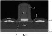
- pinch zones 6 where the thickness of semiconductor material is reduced may tend to form on either side of a region 3 of the surface layer located opposite grid and spacers 5.
- Such pinching zones 6 between this region 3 and portions 4 enriched in Germanium are illustrated on the figure 1 and pose several problems.
- the deposition of the silicon layer on the semiconductor blocks is carried out so as to completely fill said cavities.
- the growth of the second semiconductor material based on Si x Ge 1-x is carried out without doping.
- the semiconductor blocks are not doped when the thermal oxidation is carried out.
- the second semiconductor material may be different from the first semiconductor material and have a lattice parameter different from that of the first semiconductor material.
- At least one thermal annealing is carried out under a neutral atmosphere, so as to homogenize the germanium concentration of the semiconductor portions.
- the transistor produced is typically a P-type transistor.
- the Germanium-enriched semiconductor portions then make it possible to exert a compressive stress on the given region in which the channel structure is provided.
- This structure comprises a substrate of the semiconductor-on-insulator type, with a semiconductor support layer 10, typically made of silicon, an insulating layer 11 of silicon oxide arranged on the support layer 10 and a superficial semiconductor layer 12 arranged on and in contact with the insulating layer 11 and designed to receive at least one channel region of a transistor, in particular a P-type transistor, for example a PMOS.
- a semiconductor support layer 10 typically made of silicon
- an insulating layer 11 of silicon oxide arranged on the support layer 10
- a superficial semiconductor layer 12 arranged on and in contact with the insulating layer 11 and designed to receive at least one channel region of a transistor, in particular a P-type transistor, for example a PMOS.
- Gate block 22 may here be intended to form the final gate electrode of the transistor.
- Gate block 22 may for example be based on polysilicon or TiN or W or a combination of these materials.
- the spacers 23 may for example be based on SiN or SiCO or SiBCN or SiOCN or a combination of these materials.
- gate block 22 is also surmounted by at least one hard mask 24, for example formed from a layer of SiN and/or SiO 2 .
- a second semiconductor material, containing Germanium, is then grown by epitaxy on the first semiconductor material of said superficial semiconductor layer 12, which is intended to enrich the surface layer 12 with germanium.
- the second semiconductor material may be different from the first semiconductor material and have a lattice parameter different from that of the first semiconductor material.
- the second semiconductor material can be based on Si 1-x Ge x with x>0.
- the Germanium concentration x is for example between 0.05 and 0.80 and typically between 0.2 and 0.5, preferably such that x>a when the first semiconductor material is Si 1-a Ge a .
- the growth of the second semiconductor material on the first semiconductor material is typically carried out so as to form blocks 26 of the second semiconductor material having lateral facets 27 forming a non-zero angle ⁇ with a normal n at a principal plane of the surface layer (ie a plane passing through the surface layer and parallel to the plane [O; x; y] of the orthogonal reference [O; x; y; z] given on the figure 2B ).
- the growth epitaxial of this second material is preferably carried out without doping in situ so that the blocks 26 are not doped at this stage of the process.
- the blocks 26 are formed by selective epitaxy without covering the spacers 23 or the gate 22.
- the lateral facets 27 have one end located at the foot of the spacers 23.
- spaces or cavities 28 are arranged between the spacers 23 and the facets 27 of the blocks 26 of the second semiconductor material.
- these cavities 28 are then at least partially filled with the aid of a semiconductor layer 29.
- the semiconductor layer 29 is produced by deposition, in particular by epitaxial growth on the blocks 26.
- the layer 29 is at based on a material different from that of the semiconductor blocks 26 and in particular with a lower germanium concentration than that of the semiconductor blocks 26.
- the semiconductor material of the layer 29 is preferably chosen so as to be able to grow without making a facet.
- the semiconductor material of layer 29 may be silicon.
- the formation of this layer 29 can be such that portions can extend over the upper faces of the blocks 26.
- the growth of this material can optionally be carried out so that portions 29a of the layer 29 completely fill the cavities 28 ( Fig. 2C ).
- the semiconductor layer 29 is formed selectively without covering the gate 22. This epitaxial growth of the semiconductor layer 29 is preferably carried out without doping in situ.
- At least a first thermal oxidation step is carried out at a temperature that is preferably high but lower than the melting temperature of the material Si 1-x Ge x , typically at a temperature between 750° C. and 1100°C.
- the oxidation time/temperature pair depends on the thickness of the layer to be oxidized. For example, provision can be made to carry out the oxidation at a temperature of 900° C. for a period of the order of 5 min, or else at a temperature of 1050° C. for a period of the order of 20 s, for a layer with a thickness of about 6 nm of SiGe with a Germanium concentration of about 30%.
- the oxidation of the entire thickness of portions of the layer 29 located on the upper faces of blocks 26 while other portions 29a of the layer 29 which come to fill the cavities 28 and separating the side facets 27 of the spacers 23 are not yet oxidized.
- the semiconductor blocks 26 and the portions 29a then have different oxidation rates due to their respective different silicon proportions, as described in the document : “Si and SiGe: SiGe oxidation kinetics and oxide density measured by resonant soft X-ray reflectivity”, Rozé et al., Nanotechnology Material and Devices Conference 2017 .
- the oxidation is continued over the entire thickness of the blocks 26 then preferably so as to oxidize the portions 29a.
- the Germanium concentration is favored in portions 12a of the surface layer 12 further away than those directly adjacent to the access regions 12b ( figure 2E ). Because the oxidation rate depends on the Germanium content, with such an arrangement, a pinching effect as mentioned above and illustrated in the figure is avoided. figure 1 , likely to cause a discontinuity of the superficial semiconductor layer 12 and in any case to increase the channel access resistances.
- the portions 31a of lower germanium composition even typically have a greater thickness than that of parts 31b farther from the channel structure and can be produced with a thickness at least equal to or even greater than that of the access regions 12b and of the channel structure 12a.
- a deoxidation in order to remove a thickness of oxide 33 formed during the Germanium condensation can then be carried out ( figure 2F ).
- This removal can be carried out, for example, using dilute HF, with a content of, for example, 1%.
- semiconductor regions 35 can be grown by epitaxy on either side of the spacers 23 from the semiconductor portions 31a, 31b ( figure 2G ).
- a semiconductor material capable of promoting compressive stress in the channel structure is chosen.
- the semiconductor regions 35 are made of silicon germanium, preferably doped, for example with boron. In situ doping performed during the growth of the semiconductor material can be performed. A dose for example of the order of 1 e 20 at*cm ⁇ 3 can be used, for example.
- a P-type transistor formed in the Germanium-enriched superficial semiconductor layer of a semiconductor-on-insulator type substrate is particularly suitable for the implementation of circuits with low consumption (“Low Power”) and high performance (“high-performance”).
Landscapes
- Thin Film Transistor (AREA)
- Insulated Gate Type Field-Effect Transistor (AREA)
Applications Claiming Priority (1)
| Application Number | Priority Date | Filing Date | Title |
|---|---|---|---|
| FR2008832A FR3113767B1 (fr) | 2020-08-31 | 2020-08-31 | Procede ameliore d’enrichissement germanium autour du canal d’un transistor |
Publications (1)
| Publication Number | Publication Date |
|---|---|
| EP3961721A1 true EP3961721A1 (de) | 2022-03-02 |
Family
ID=74183238
Family Applications (1)
| Application Number | Title | Priority Date | Filing Date |
|---|---|---|---|
| EP21188650.2A Pending EP3961721A1 (de) | 2020-08-31 | 2021-07-30 | Verbessertes verfahren zur germaniumanreicherung um den kanal eines transistors |
Country Status (3)
| Country | Link |
|---|---|
| US (1) | US11646196B2 (de) |
| EP (1) | EP3961721A1 (de) |
| FR (1) | FR3113767B1 (de) |
Families Citing this family (1)
| Publication number | Priority date | Publication date | Assignee | Title |
|---|---|---|---|---|
| FR3113767B1 (fr) * | 2020-08-31 | 2022-12-02 | Commissariat Energie Atomique | Procede ameliore d’enrichissement germanium autour du canal d’un transistor |
Citations (5)
| Publication number | Priority date | Publication date | Assignee | Title |
|---|---|---|---|---|
| US20080042209A1 (en) | 2006-08-16 | 2008-02-21 | Chartered Semiconductor Manufacturing Ltd. | Semiconductor system using germanium condensation |
| US20110024804A1 (en) * | 2009-07-28 | 2011-02-03 | Taiwan Semiconductor Manufacturing Company, Ltd. | Method for forming high germanium concentration sige stressor |
| US20130069123A1 (en) * | 2011-09-16 | 2013-03-21 | Globalfoundries Inc. | Cmos semiconductor devices having stressor regions and related fabrication methods |
| US20130175606A1 (en) * | 2012-01-06 | 2013-07-11 | International Business Machines Corporation | Integrated circuit having raised source drains devices with reduced silicide contact resistance and methods to fabricate same |
| US20200111870A1 (en) * | 2018-10-04 | 2020-04-09 | Globalfoundries Inc. | Epitaxial semiconductor material grown with enhanced local isotropy |
Family Cites Families (1)
| Publication number | Priority date | Publication date | Assignee | Title |
|---|---|---|---|---|
| FR3113767B1 (fr) * | 2020-08-31 | 2022-12-02 | Commissariat Energie Atomique | Procede ameliore d’enrichissement germanium autour du canal d’un transistor |
-
2020
- 2020-08-31 FR FR2008832A patent/FR3113767B1/fr active Active
-
2021
- 2021-07-30 EP EP21188650.2A patent/EP3961721A1/de active Pending
- 2021-08-24 US US17/445,747 patent/US11646196B2/en active Active
Patent Citations (5)
| Publication number | Priority date | Publication date | Assignee | Title |
|---|---|---|---|---|
| US20080042209A1 (en) | 2006-08-16 | 2008-02-21 | Chartered Semiconductor Manufacturing Ltd. | Semiconductor system using germanium condensation |
| US20110024804A1 (en) * | 2009-07-28 | 2011-02-03 | Taiwan Semiconductor Manufacturing Company, Ltd. | Method for forming high germanium concentration sige stressor |
| US20130069123A1 (en) * | 2011-09-16 | 2013-03-21 | Globalfoundries Inc. | Cmos semiconductor devices having stressor regions and related fabrication methods |
| US20130175606A1 (en) * | 2012-01-06 | 2013-07-11 | International Business Machines Corporation | Integrated circuit having raised source drains devices with reduced silicide contact resistance and methods to fabricate same |
| US20200111870A1 (en) * | 2018-10-04 | 2020-04-09 | Globalfoundries Inc. | Epitaxial semiconductor material grown with enhanced local isotropy |
Non-Patent Citations (3)
| Title |
|---|
| ROZÉ ET AL.: "Si et SiGe : SiGe oxidation kinetics and oxide density measured by resonant soft X-ray reflectivity", NANOTECHNOLOGY MATERIAL AND DEVICES CONFÉRENCE, 2017 |
| TEZUKA ET AL.: "A novel fabrication technique of ultrathin and relaxed SiGe buffer layers with high Ge fraction for sub-100 nm strained silicon on insulator MOSFETs", JAPANESE JOURNAL OF APPLIED PHYSICS, vol. 40, 2001, pages 2866 - 2874, XP001081002, DOI: 10.1143/JJAP.40.2866 |
| TEZUKA ET AL.: "Selectively formed high mobility SiGe on Insulator pMOSFETs with Ge-rich strained surface channels using local condensation technique", SYMPOSIUM ON VLSI TECHNOLOGY, 2004 |
Also Published As
| Publication number | Publication date |
|---|---|
| FR3113767A1 (fr) | 2022-03-04 |
| FR3113767B1 (fr) | 2022-12-02 |
| US11646196B2 (en) | 2023-05-09 |
| US20220068638A1 (en) | 2022-03-03 |
Similar Documents
| Publication | Publication Date | Title |
|---|---|---|
| EP1837916B1 (de) | Verfahren zum Herstellen eines Transistors mit einem Germanium enthaltenden Kanal | |
| EP1266409B1 (de) | Mos-transistor mit metallischen source- und draingebieten und dessen herstellungsverfahren | |
| EP2075826B1 (de) | Verfahren zur Herstellung eines Halbleiter-auf-Isolator-Substrats, das eine Anreicherungsetappe mit lokalisiertem Germanium umfasst | |
| FR3060840A1 (fr) | Procede de realisation d'un dispositif semi-conducteur a espaceurs internes auto-alignes | |
| FR2799305A1 (fr) | Procede de fabrication d'un dispositif semi-conducteur a grille enveloppante et dispositif obtenu | |
| FR3060841A1 (fr) | Procede de realisation d'un dispositif semi-conducteur a espaceurs internes auto-alignes | |
| WO2008054967A2 (en) | Method for providing a nanoscale, high electron mobility transistor (hemt) on insulator | |
| EP2835832A2 (de) | Verbessertes Verfahren zur Herstellung von dotierten Zonen und/oder Zonen, die eine Spannung unter den Abstandhaltern eines Transistors ausüben | |
| EP1830400A1 (de) | Verfahren zur Herstellung eines Substrats durch Germaniumkondensation | |
| EP3376545B1 (de) | Transistor mit strukturierten source- und drain-bereichen, und sein bearbeitungsverfahren | |
| EP3079168A1 (de) | Dotierverfahren von source- und drain-bereichen eines transistors mithilfe einer selektiven amorphisierung | |
| JP2015008291A (ja) | 歪み半導体構造を形成する方法 | |
| EP3026711B1 (de) | Verbessertes verfahren zur erzeugung einer dehnung in einem transistorkanal mithilfe von opfer-source- und opfer-drain-schichten und einem gate-austausch | |
| EP1638149B1 (de) | Verfahren zur Herstellung eines Feldefekttransistors mit isoliertem Gatter und Heterostruktur-Kanal | |
| EP3961721A1 (de) | Verbessertes verfahren zur germaniumanreicherung um den kanal eines transistors | |
| EP3961720B1 (de) | Germaniumanreicherung um den kanal herum durch erhöhte blöcke | |
| EP1407486B1 (de) | Herstellungsverfahren für einen transistor auf einem soi-substrat | |
| EP3671826B1 (de) | Verbessertes herstellungsverfahren eines integrierten schaltkreises, der einen nmos- und einen pmos-transistor umfasst | |
| FR3027451A1 (fr) | Substrat et procede de fabrication d'un substrat | |
| FR2887370A1 (fr) | Procede de fabrication d'un transistor isole a canal contraint | |
| JP2022067962A (ja) | Soiウェーハの製造方法及びsoiウェーハ | |
| EP3859769B1 (de) | Verfahren zum ätzen im nanometerbereich einer germanium-zinn-legierung (gesn) für fet-transistor | |
| FR3098014A1 (fr) | Composé intermétallique | |
| FR3164835A1 (fr) | Procédé de réalisation d’un dispositif à transistors CFET | |
| FR3166240A1 (fr) | Substrat intermediaire pour la fabrication d’un substrat pour transistor a haute mobilite d’electrons |
Legal Events
| Date | Code | Title | Description |
|---|---|---|---|
| PUAI | Public reference made under article 153(3) epc to a published international application that has entered the european phase |
Free format text: ORIGINAL CODE: 0009012 |
|
| STAA | Information on the status of an ep patent application or granted ep patent |
Free format text: STATUS: REQUEST FOR EXAMINATION WAS MADE |
|
| 17P | Request for examination filed |
Effective date: 20210730 |
|
| AK | Designated contracting states |
Kind code of ref document: A1 Designated state(s): AL AT BE BG CH CY CZ DE DK EE ES FI FR GB GR HR HU IE IS IT LI LT LU LV MC MK MT NL NO PL PT RO RS SE SI SK SM TR |
|
| STAA | Information on the status of an ep patent application or granted ep patent |
Free format text: STATUS: EXAMINATION IS IN PROGRESS |
|
| RAP3 | Party data changed (applicant data changed or rights of an application transferred) |
Owner name: COMMISSARIAT A L'ENERGIE ATOMIQUE ET AUX ENERGIESALTERNATIVES |
|
| 17Q | First examination report despatched |
Effective date: 20241018 |
|
| REG | Reference to a national code |
Ref country code: DE Ref legal event code: R079 Free format text: PREVIOUS MAIN CLASS: H01L0029660000 Ipc: H10D0030010000 |
|
| GRAP | Despatch of communication of intention to grant a patent |
Free format text: ORIGINAL CODE: EPIDOSNIGR1 |
|
| STAA | Information on the status of an ep patent application or granted ep patent |
Free format text: STATUS: GRANT OF PATENT IS INTENDED |
|
| RIC1 | Information provided on ipc code assigned before grant |
Ipc: H10D 30/01 20250101AFI20260127BHEP Ipc: H10D 30/67 20250101ALI20260127BHEP Ipc: H10D 30/69 20250101ALI20260127BHEP Ipc: H10D 62/822 20250101ALI20260127BHEP |