EP1830400A1 - Verfahren zur Herstellung eines Substrats durch Germaniumkondensation - Google Patents
Verfahren zur Herstellung eines Substrats durch Germaniumkondensation Download PDFInfo
- Publication number
- EP1830400A1 EP1830400A1 EP07354007A EP07354007A EP1830400A1 EP 1830400 A1 EP1830400 A1 EP 1830400A1 EP 07354007 A EP07354007 A EP 07354007A EP 07354007 A EP07354007 A EP 07354007A EP 1830400 A1 EP1830400 A1 EP 1830400A1
- Authority
- EP
- European Patent Office
- Prior art keywords
- germanium
- silicon
- temperature
- layer
- order
- Prior art date
- Legal status (The legal status is an assumption and is not a legal conclusion. Google has not performed a legal analysis and makes no representation as to the accuracy of the status listed.)
- Withdrawn
Links
Images


Classifications
-
- H—ELECTRICITY
- H10—SEMICONDUCTOR DEVICES; ELECTRIC SOLID-STATE DEVICES NOT OTHERWISE PROVIDED FOR
- H10P—GENERIC PROCESSES OR APPARATUS FOR THE MANUFACTURE OR TREATMENT OF DEVICES COVERED BY CLASS H10
- H10P90/00—Preparation of wafers not covered by a single main group of this subclass, e.g. wafer reinforcement
- H10P90/19—Preparing inhomogeneous wafers
- H10P90/1904—Preparing vertically inhomogeneous wafers
- H10P90/1906—Preparing SOI wafers
-
- H—ELECTRICITY
- H10—SEMICONDUCTOR DEVICES; ELECTRIC SOLID-STATE DEVICES NOT OTHERWISE PROVIDED FOR
- H10W—GENERIC PACKAGES, INTERCONNECTIONS, CONNECTORS OR OTHER CONSTRUCTIONAL DETAILS OF DEVICES COVERED BY CLASS H10
- H10W10/00—Isolation regions in semiconductor bodies between components of integrated devices
- H10W10/10—Isolation regions comprising dielectric materials
- H10W10/181—Semiconductor-on-insulator [SOI] isolation regions, e.g. buried oxide regions of SOI wafers
Definitions
- microelectronics industry then turned to germanium, which is fully compatible with the technology developed for silicon and has the same crystalline structure as silicon, but with better properties especially in terms of charge carrier mobility.
- pMOSFET metal oxide semiconductor field effect transistors
- metal oxide semiconductor field effect transistors metal oxide semiconductor field effect transistors
- pMOSFET metal oxide semiconductor field effect transistors
- FD pMOSFET charge carriers
- germanium on insulator substrates For the production of germanium on insulator substrates (GOI or GeOI: “Germanium On Insulator”), a first technique uses the “Smart Cut” (registered trademark) technology, initially developed for the manufacture of silicon-on-insulator substrates (SOI: “ Silicon On Insulator "), described in particular in the article “200mm Germanium-On-Insulator (GeOI) structures realized from epitaxial wafers using the Smart Cut TM technology” by C. Deguet et al. (Proceedings ECS 2005, Quebec ).
- This technology is based on the transfer, on a silicon substrate, of a germanium layer deposited on a layer of silicon oxide forming an insulating layer.
- the GOI substrate thus obtained is of the full plate type.
- this technology has a very high cost and nMOSFET transistors are very difficult to achieve.
- a second technology is based on the principle of lateral recrystallization, in particular described in the article "High-quality single-crystal Ge on insulator by liquid-phase epitaxy on Si substrates" by Y. Liu et al. (Applied Physics Letters, vol.84, No. 14, April 5, 2004 ), making it possible to produce a GOI substrate of the localized type.
- the technique involves depositing locally on a standard silicon substrate a layer of nitride, which will form the insulator, and then depositing on top a larger layer of germanium, which will then be locally in contact with the substrate. silicon. Once encapsulated, the stack is briefly heated to the melting temperature of the germanium and then cooled.
- a third known manufacturing technique uses the germanium condensation technique, which also makes it possible to produce localized GOI substrates. This technique is based on the total miscibility of germanium and silicon (same crystalline structure) and on the difference in chemical affinities between germanium and silicon with respect to oxygen, as highlighted in the article. "Novel Technical Fabrication of Ultrathin and Relaxed SiGe Buffer Layers with High Ge Fraction for Sub-100nm Strained Silicon-On-Insulator MOSFETs" by T. Tezuka et al. (Jpn J. Appl Physics Vol 40 (2001) pp.2866-2874 Part 1, No. 4B, April 2001 ).
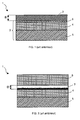
- the fabrication of a substrate 1 comprising a silicon and germanium on insulator compound and of Si 1 -Xf Ge Xf type , with a final concentration Xf of germanium between a first non-zero value and 1, comprises the formation of a silicon-germanium alloy layer 2 of Si 1-Xi Ge Xi type , with an initial concentration Xi of germanium strictly between 0 and Xf.
- the layer 2 of Si 1-Xi , Ge Xi is deposited on a substrate 3 in SOI comprising a layer 4 of silicon oxide SiO 2 , buried between two silicon layers 5 and forming an insulator for the substrate 3 in SOI (FIG. 1).
- the second step consists in carrying out a heat oxidation treatment, preferably at a high temperature, of silicon of the layer 2 made of Si 1-Xi Ge Xi . Since silicon has a better chemical affinity for oxygen, germanium is not oxidized. As represented in FIG. 2, the thermal oxidation then leads to the consumption of the silicon of the whole of the stack of the substrate 3 in SOI and of the layer 2 to Si 1-xi Ge xi , to form an upper layer 6 of SiO 2 , disposed on the top of the substrate 1.
- the silicon layer 5 initially disposed between the Si 1-x Ge xi layer 2 and the buried SiO 2 layer 4 has been consumed during the thermal oxidation and is recovered in the upper layer 6 in SiO 2 .
- the germanium not being soluble in SiO 2 a layer 7 enriched in germanium, forming the Si 1-x Ge xh compound, was rejected against the buried SiO 2 layer 4 and has a final thickness. Ef, lower than the initial thickness Ei of the layer 2 in Si 1-xi Ge xi .
- the germanium condensation process can continue until the complete consumption of the silicon, so as to obtain a layer 7 exclusively comprising germanium, to form a compound in GOI, with a final concentration Xf of germanium equal to 1.
- the layer 7 then forms a compound in SGOI with a final concentration Xf of germanium strictly between 0 and 1.
- the article "Relaxed silicon-germanium-on-insulator fabricated by oxygen implantation and oxidation-enhanced annealing" by Zhijun et al. describes another method of producing a substrate made of SGOI, comprising a step of depositing a Si 1-x Ge x layer on a silicon substrate, followed by an ion implantation step and a step thermal oxidation at a temperature of 1000 ° C under pure oxygen. Then, the method comprises an argon annealing heat treatment step, combined with 1% oxygen, at high temperature, of the order of 1300 ° C.
- such a production method proves, on the one hand, difficult to implement and, on the other hand, does not allow to obtain a substrate 1 of good quality.
- the object of the invention is to remedy all of the above-mentioned drawbacks and relates to a method of manufacturing a substrate comprising a silicon and germanium on insulator compound and of Si 1-Xf Ge Xh type which is easy to put into practice. which has optimum characteristics in terms of germanium concentration.
- the first thermal oxidation step comprises at least one thermal treatment step under inert gas at said first predetermined oxidation temperature.
- the manufacturing method is intended to produce a substrate 1 made of silicon and germanium on insulator (SGOI) or germanium on insulator (GOI), namely comprising a silicon and germanium on insulator compound and type Si 1-Xf Ge Xf .
- the final concentration Xf of germanium is strictly between 0 and 1, for a substrate in SGOI, and the final concentration Xf of germanium is equal to 1, for a GOI substrate.
- the manufacturing method comprises first the formation of the substrate on insulator 3 and the formation, for example by epitaxy, of the silicon-germanium alloy layer 2 of Si 1-xi Ge xi type (FIG. 1). The method then comprises a thermal oxidation treatment of silicon, preferably carried out at high temperature and consisting in particular of injecting an oxidizing gas inside, for example, an enclosure, in which the manufacturing process is carried out. of the substrate 1.
- a first step Ox1 of thermal oxidation of the silicon of the layer 2 comprises a preliminary step P0 of increasing the temperature, between the times t0 and t1, carried out under inert gas, for example nitrogen, carbon dioxide, helium or argon, under oxygen or a mixture of oxygen and inert gas.
- the preliminary step P0 makes it possible to reach the first predetermined oxidation temperature T1, which is preferably lower than the melting point of the silicon-germanium alloy of the layer 2 in Si 1-xi Ge xi .
- the first thermal oxidation step Ox1 then comprises a first thermal oxidation period P1 at the temperature T1, between the instants t1 and t2, followed by a first period P2 of heat treatment under inert gas, between the instants t2 and t3, performed at the same temperature, namely at the first predetermined oxidation temperature T1.
- inert gas means a pure inert gas, that is to say an inactive gas which does not react with the compounds of the layers of the substrate, more particularly a gas comprising 0% oxygen.
- the thermal treatment step under inert gas consists of stopping the injection of oxidizing gas, participating in the oxidation step, and injecting pure inert gas in the place of the oxidizing gas, during a predetermined time and at the same temperature as for oxidation.
- inert gas at the predetermined temperature T1 allows in particular the diffusion and homogenization of the germanium concentration in the layer 7 in forming the substrate 1.
- a second thermal oxidation period P3 between instants t3 and t4 is then performed after the first thermal treatment period P2 under inert gas, at the first oxidation temperature T1. predetermined. Then, a second period P4 of heat treatment under inert gas is performed between times t4 and t5, as described above. A third thermal oxidation period P5, between instants t5 and t6, is then carried out following the second thermal treatment period P4 under an inert gas.
- the first thermal oxidation step Ox1 interspersed with several periods of heat treatment under pure inert gas is thus carried out as long as the desired final concentration Xf of germanium remains below the concentration leading to the melting of the silicon alloy. and germanium at the first predetermined oxidation temperature T1.
- the initial thickness Ei of the layer 2 in Si 1-Xi Ge Xi is chosen as a function of the final thickness Ef desired of the layer 7 in Si 1-Xf Ge Xf ' Plus the initial thickness Ei is thick, plus the final thickness Ef will be thick, the initial thickness Ei of the layer 2 in Si 1-Xi Ge Xi must always be less than the critical thickness of plastic relaxation. Moreover, the final thickness E f of the layer 7 of Si 1-Xf Ge Xf also depends on the enrichment rate, the final concentration Xf being reached more rapidly if the initial concentration Xi is large.
- the first predetermined oxidation temperature T1 is of the order of 900 ° C to 1200 ° C, and is preferably between 1025 ° C and 1075 ° C.
- the initial thickness Ei of the layer 2 in Si 1-xi Ge xi is of the order of 100nm, of the order of 50nm or of the order of 30nm and the initial concentration Xi of germanium of the layer 2 in Si 1-xi Ge xi is, respectively, of the order of 10%, of the order 20% or in the order of 30%.
- the first thermal oxidation step Ox1 comprises thermal oxidation periods of the order of 15 min, 87 min and 86 min, for a total duration of 188 min, interspersed with three stages of heat treatment under pure inert gas of the order of 120min each.
- the manufacturing method according to the invention makes it possible in particular to obtain a layer 7 enriched in germanium of final thickness Ef less than the thickness initial Ei of the layer 2 and to avoid during the enrichment plastic relaxation constraints related to the concentration gradient in the layer 7 thus formed. This results in a substrate 1 with optimum qualities in terms of homogenization of the germanium concentration.
- a single treatment period inert gas can be performed during the first step Ox1 thermal oxidation.
- the period of heat treatment under pure inert gas then has a sufficient duration, to completely consume the silicon of the layer 2 Si 1-Xj Ge Xi , to achieve the desired final concentration Xf germanium and homogenize the composition of the layer 7 in Si 1-Xf Ge Xf thus formed (FIG. 2).
- a thermal treatment period under pure inert gas can be carried out just after the prior period P0 for raising the temperature of the first thermal oxidation step Ox1.
- the alternation between the thermal treatment steps under inert gas and the thermal oxidation periods then takes place as before, at the predetermined oxidation temperature T1.
- the periods P1, P3 and P5 are periods of thermal treatment under inert gas and the periods P2, P4 are periods of thermal oxidation.
- the first treatment period following the rise in temperature, is a heat treatment period under inert gas and the first thermal continuous oxidation step Ox1, without be cut by other heat treatment steps under inert gas.
- the thermal oxidation treatment comprises a second thermal oxidation step Ox2, carried out at a second predetermined oxidation temperature T2, just after the first thermal oxidation step Ox1.
- the second predetermined oxidation temperature T2 is lower than the melting temperature of the alloy Si 1-xi Ge xi and, for example, lower than the first predetermined oxidation temperature T1.
- the thermal oxidation treatment thus comprises a first thermal oxidation step Ox1, for example with the prior step P0 of temperature rise, between times t0 and t1, and thermal oxidation periods P1, P3, respectively between instants t1 and t2 and instants t3 and t4, interspersed with a period P2 of heat treatment under inert gas, between times t2 and t3.
- the thermal oxidation treatment then comprises a second thermal oxidation step Ox2 comprising an intermediate period P4, by for example, the temperature drops between times t4 and t5 until the second predetermined oxidation temperature T2 is reached.
- the second thermal oxidation step Ox2 then comprises, for example, a first thermal oxidation period P5, between instants t5 and t6, followed by a period P6 of heat treatment under pure inert gas, between times t6 and t7.
- the second thermal oxidation step Ox2 continues on, with periods of thermal oxidation interspersed with periods of heat treatment under inert gas, as long as the desired final concentration Xf of germanium in the layer 7 in Si 1-xf Ge xf is still not reached.
- the first predetermined oxidation temperature T1 is of the order of 1050 ° C and the second predetermined oxidation temperature T2 is of the order of 900 ° C.
- the maximum concentration of germanium that can be obtained is 65%, to avoid melting of the alloy.
- the oxidation temperature for example up to the value T2 of the order of 900 ° C., which makes it possible to obtain a layer 7 of pure germanium, the second oxidation temperature T2 remaining below the melting temperature of pure germanium.
- the thermal oxidation treatment may comprise several other thermal oxidation steps, after the second thermal oxidation step Ox2, each interspersed with one or more stages of heat treatment under gas. pure inert.
- the various additional thermal oxidation steps are then preferably performed at predetermined predetermined oxidation temperatures of the first T1 and second T2 predetermined oxidation temperatures and, preferably, with decreasing values.
- the method of manufacturing the substrate 1 may comprise a low-temperature thermal oxidation treatment, making it possible to avoid the consumption of germanium during the different steps of the germanium condensation process.
- the low temperature thermal oxidation treatment is carried out at a temperature of, for example, 700 ° C to 900 ° C and preferably at the beginning of the germanium condensation process.
- the low temperature oxidation step can be carried out irrespective of the number of thermal oxidation steps (FIG. 4) and regardless of the number of treatment steps under inert gas (FIGS. 3 and 4). .
- the alternative embodiment of the process for manufacturing the substrate 1 differs from the manufacturing processes described above by the deposition of an additional layer 8 of silicon formed on the layer 2 made of Si 1-Xi Ge Xi , before the thermal oxidation treatment to form the layer 7 in Si 1-Xf Ge Xf .
- the additional layer 8 has a thickness, for example, of the order of a few angstroms to a few nanometers and allows in particular to form a thin layer of SiO 2 on top of the substrate 1, preventing the consumption of germanium during the first periods of time. thermal oxidation.
- such a method makes it possible in particular to manufacture a GOI substrate or an SGOI substrate having optimum characteristics in terms of the concentration of germanium, in order to avoid any problem due to stress relaxation inside the layer 7 formed by germanium condensation. Furthermore, such a manufacturing method can be implemented regardless of the desired thickness of the substrate 1 and layers 2 in Si 1-xi Ge xi and 7 in Si 1-xf Ge xf .
- the invention is not limited to the various embodiments described above.
- the values of the germanium concentrations, treatment times and layer thicknesses are non-limiting and depend on the desired initial and final characteristics of the substrate 1. It is possible to produce a calibration curve making it possible to quickly define the different values of the periods of time. final treatment and concentration of germanium, depending in particular on the predetermined oxidation temperatures.
- the nitrogen can be replaced by any pure inert gas, for example, argon, helium, hydrogen or a mixture of hydrogen and nitrogen.
- the second predetermined oxidation temperature T2 may be greater than the first predetermined oxidation temperature T1, as long as it remains below the melting temperature of the Si 1-xi Ge xi alloy of the layer 2.
- the first thermal oxidation step Ox1 may comprise additional periods of thermal oxidation (not shown) interspersed with additional periods of heat treatment under inert gas (not shown).
- the period P5 of the second thermal oxidation step Ox2 may be a thermal treatment period under inert gas and the period P6 may be a thermal oxidation period.
- the second thermal oxidation step Ox2 can be interspersed with a heat treatment step under inert gas or several heat treatment steps under inert gas.
Landscapes
- Recrystallisation Techniques (AREA)
- Thin Film Transistor (AREA)
Applications Claiming Priority (1)
| Application Number | Priority Date | Filing Date | Title |
|---|---|---|---|
| FR0601850A FR2898215B1 (fr) | 2006-03-01 | 2006-03-01 | Procede de fabrication d'un substrat par condensation germanium |
Publications (1)
| Publication Number | Publication Date |
|---|---|
| EP1830400A1 true EP1830400A1 (de) | 2007-09-05 |
Family
ID=37049902
Family Applications (1)
| Application Number | Title | Priority Date | Filing Date |
|---|---|---|---|
| EP07354007A Withdrawn EP1830400A1 (de) | 2006-03-01 | 2007-02-13 | Verfahren zur Herstellung eines Substrats durch Germaniumkondensation |
Country Status (3)
| Country | Link |
|---|---|
| US (1) | US20070207598A1 (de) |
| EP (1) | EP1830400A1 (de) |
| FR (1) | FR2898215B1 (de) |
Families Citing this family (11)
| Publication number | Priority date | Publication date | Assignee | Title |
|---|---|---|---|---|
| JP4413580B2 (ja) * | 2003-11-04 | 2010-02-10 | 株式会社東芝 | 素子形成用基板の製造方法 |
| JP4427489B2 (ja) * | 2005-06-13 | 2010-03-10 | 株式会社東芝 | 半導体装置の製造方法 |
| FR2902234B1 (fr) * | 2006-06-12 | 2008-10-10 | Commissariat Energie Atomique | PROCEDE DE REALISATION DE ZONES A BASE DE Si1-yGey DE DIFFERENTES TENEURS EN Ge SUR UN MEME SUBSTRAT PAR CONDENSATION DE GERMANIUM |
| EP1868233B1 (de) | 2006-06-12 | 2009-03-11 | Commissariat A L'energie Atomique | Verfahren zur Herstellung von auf Si1-yGey basierenden Zonen mit unterschiedlichen Ge-Gehalten auf ein und demselben Substrat mittels Kondensation von Germanium |
| FR2935194B1 (fr) * | 2008-08-22 | 2010-10-08 | Commissariat Energie Atomique | Procede de realisation de structures geoi localisees, obtenues par enrichissement en germanium |
| DE102009010883B4 (de) * | 2009-02-27 | 2011-05-26 | Amd Fab 36 Limited Liability Company & Co. Kg | Einstellen eines nicht-Siliziumanteils in einer Halbleiterlegierung während der FET-Transistorherstellung mittels eines Zwischenoxidationsprozesses |
| US8623728B2 (en) * | 2009-07-28 | 2014-01-07 | Taiwan Semiconductor Manufacturing Company, Ltd. | Method for forming high germanium concentration SiGe stressor |
| US9299809B2 (en) | 2012-12-17 | 2016-03-29 | Globalfoundries Inc. | Methods of forming fins for a FinFET device wherein the fins have a high germanium content |
| CN103474386B (zh) * | 2013-09-26 | 2016-02-03 | 中国科学院上海微系统与信息技术研究所 | 一种利用C掺杂SiGe调制层制备SGOI或GOI的方法 |
| US10164103B2 (en) | 2016-10-17 | 2018-12-25 | International Business Machines Corporation | Forming strained channel with germanium condensation |
| CN112908849A (zh) * | 2021-01-28 | 2021-06-04 | 上海华力集成电路制造有限公司 | 一种形成SiGe沟道的热处理方法 |
Citations (1)
| Publication number | Priority date | Publication date | Assignee | Title |
|---|---|---|---|---|
| US20050003229A1 (en) * | 2003-07-01 | 2005-01-06 | International Business Machines Corporation | Defect reduction by oxidation of silicon |
Family Cites Families (2)
| Publication number | Priority date | Publication date | Assignee | Title |
|---|---|---|---|---|
| US7029980B2 (en) * | 2003-09-25 | 2006-04-18 | Freescale Semiconductor Inc. | Method of manufacturing SOI template layer |
| JP4413580B2 (ja) * | 2003-11-04 | 2010-02-10 | 株式会社東芝 | 素子形成用基板の製造方法 |
-
2006
- 2006-03-01 FR FR0601850A patent/FR2898215B1/fr not_active Expired - Fee Related
-
2007
- 2007-02-13 EP EP07354007A patent/EP1830400A1/de not_active Withdrawn
- 2007-02-16 US US11/707,072 patent/US20070207598A1/en not_active Abandoned
Patent Citations (1)
| Publication number | Priority date | Publication date | Assignee | Title |
|---|---|---|---|---|
| US20050003229A1 (en) * | 2003-07-01 | 2005-01-06 | International Business Machines Corporation | Defect reduction by oxidation of silicon |
Non-Patent Citations (3)
| Title |
|---|
| SPADAFORA M ET AL: "Oxidation rate enhancement of SiGe epitaxial films oxidized in dry ambient", APPLIED PHYSICS LETTERS AIP USA, vol. 83, no. 18, 3 November 2003 (2003-11-03), pages 3713 - 3715, XP002401903, ISSN: 0003-6951 * |
| SUGIYAMA N ET AL: "Temperature effects on Ge condensation by thermal oxidation of SiGe-on-insulator structures", JOURNAL OF APPLIED PHYSICS AIP USA, vol. 95, no. 8, 15 April 2004 (2004-04-15), pages 4007 - 4011, XP002401902, ISSN: 0021-8979 * |
| ZHIJUN CHEN ET AL: "Relaxed silicon-germanium-on-insulator fabricated by oxygen implantation and oxidation-enhanced annealing", SEMICONDUCTOR SCIENCE AND TECHNOLOGY IOP PUBLISHING UK, vol. 20, no. 8, August 2005 (2005-08-01), pages 770 - 774, XP002401901, ISSN: 0268-1242 * |
Also Published As
| Publication number | Publication date |
|---|---|
| US20070207598A1 (en) | 2007-09-06 |
| FR2898215B1 (fr) | 2008-05-16 |
| FR2898215A1 (fr) | 2007-09-07 |
Similar Documents
| Publication | Publication Date | Title |
|---|---|---|
| EP1830400A1 (de) | Verfahren zur Herstellung eines Substrats durch Germaniumkondensation | |
| EP1830401B1 (de) | Mikrostruktur zur Bildung eines Substrats aus Silizium und Germanium auf einem Isolator und vom Typ Si1-XGeX | |
| US8110486B2 (en) | Method of manufacturing semiconductor wafer by forming a strain relaxation SiGe layer on an insulating layer of SOI wafer | |
| EP1837916B1 (de) | Verfahren zum Herstellen eines Transistors mit einem Germanium enthaltenden Kanal | |
| US6723541B2 (en) | Method of producing semiconductor device and semiconductor substrate | |
| US7989327B2 (en) | Manufacturing method for a semi-conductor on insulator substrate comprising a localised Ge enriched step | |
| JP5336118B2 (ja) | マイクロエレクトロニクス及びオプトエレクトロニクス向けsoi基板の製造方法 | |
| EP0780889B1 (de) | Verfahren zur selektiven Abscheidung von Siliciden hochschmelzender Metalle auf Silizium | |
| EP1865551A2 (de) | Verfahren zur Begrenzung der Diffusion im Lückenmodus in einer Heterostruktur | |
| FR2892230A1 (fr) | Traitement d'une couche de germamium | |
| KR20110003522A (ko) | 기판상에 게르마늄층을 포함하는 구조를 제조하기 위한 프로세스 | |
| EP0976149B1 (de) | Verfahren zur verminderung der interdiffusion in einem halbleiterbauelement mit si/sige verbindungs-gatter | |
| TW201709333A (zh) | 製造絕緣體覆矽鍺之方法 | |
| FR2907966A1 (fr) | Procede de fabrication d'un substrat. | |
| WO2000077846A1 (fr) | Procede de fabrication d'un substrat de silicium comportant une mince couche d'oxyde de silicium ensevelie | |
| EP3671826B1 (de) | Verbessertes herstellungsverfahren eines integrierten schaltkreises, der einen nmos- und einen pmos-transistor umfasst | |
| EP3961721A1 (de) | Verbessertes verfahren zur germaniumanreicherung um den kanal eines transistors | |
| FR2853452A1 (fr) | Procede de fabrication d'un dispositif semiconducteur comprenant un dielectrique de grille en materiau a haute permittivite dielectrique | |
| EP2109884B1 (de) | Verfahren zur herstellung einer germaniumschicht aus einem silicium-germanium-substrat auf einem isolator | |
| EP1798761A2 (de) | Herstellungsverfahren für ein Bauelement mit mindestens einer einkristallinen Schicht auf einem Substrat | |
| WO2001099179A1 (fr) | Procede de fabrication d'un substrat semi-conducteur du type silicium sur isolant à couche active semi-conductrice mince | |
| EP3136429A1 (de) | Anordnung von ohmschen kontakten für eine vorrichtung, die einen bereich aus iii-v-halbleitermaterial und einen bereich aus einem anderen halbleitermaterial enthält | |
| FR2964495A1 (fr) | Procede de fabrication d'une structure seoi multiple comportant une couche isolante ultrafine | |
| EP3961720A1 (de) | Germaniumanreicherung um den kanal herum durch erhöhte blöcke | |
| FR2922361A1 (fr) | Procede de realisation d'un dispositif a effet de champ a canal germanium sur isolant. |
Legal Events
| Date | Code | Title | Description |
|---|---|---|---|
| PUAI | Public reference made under article 153(3) epc to a published international application that has entered the european phase |
Free format text: ORIGINAL CODE: 0009012 |
|
| AK | Designated contracting states |
Kind code of ref document: A1 Designated state(s): AT BE BG CH CY CZ DE DK EE ES FI FR GB GR HU IE IS IT LI LT LU LV MC NL PL PT RO SE SI SK TR |
|
| AX | Request for extension of the european patent |
Extension state: AL BA HR MK YU |
|
| 17P | Request for examination filed |
Effective date: 20080226 |
|
| AKX | Designation fees paid |
Designated state(s): AT BE BG CH CY CZ DE DK EE ES FI FR GB GR HU IE IS IT LI LT LU LV MC NL PL PT RO SE SI SK TR |
|
| 17Q | First examination report despatched |
Effective date: 20090513 |
|
| RAP1 | Party data changed (applicant data changed or rights of an application transferred) |
Owner name: COMMISSARIAT A L'ENERGIE ATOMIQUE ET AUX ENERGIES |
|
| STAA | Information on the status of an ep patent application or granted ep patent |
Free format text: STATUS: THE APPLICATION IS DEEMED TO BE WITHDRAWN |
|
| 18D | Application deemed to be withdrawn |
Effective date: 20120904 |