EP3965177A1 - Resistiver speicher mit einer schaltzone zwischen zwei dielektrischen bereichen mit unterschiedlichen dotierungen und/oder dielektrizitätskonstanten - Google Patents
Resistiver speicher mit einer schaltzone zwischen zwei dielektrischen bereichen mit unterschiedlichen dotierungen und/oder dielektrizitätskonstanten Download PDFInfo
- Publication number
- EP3965177A1 EP3965177A1 EP21192810.6A EP21192810A EP3965177A1 EP 3965177 A1 EP3965177 A1 EP 3965177A1 EP 21192810 A EP21192810 A EP 21192810A EP 3965177 A1 EP3965177 A1 EP 3965177A1
- Authority
- EP
- European Patent Office
- Prior art keywords
- region
- electrode
- dielectric
- interface
- layer
- Prior art date
- Legal status (The legal status is an assumption and is not a legal conclusion. Google has not performed a legal analysis and makes no representation as to the accuracy of the status listed.)
- Pending
Links
- 230000015654 memory Effects 0.000 title claims abstract description 58
- 239000000203 mixture Substances 0.000 claims abstract description 21
- 239000003989 dielectric material Substances 0.000 claims description 49
- XUIMIQQOPSSXEZ-UHFFFAOYSA-N Silicon Chemical compound [Si] XUIMIQQOPSSXEZ-UHFFFAOYSA-N 0.000 claims description 34
- 229910000449 hafnium oxide Inorganic materials 0.000 claims description 29
- WIHZLLGSGQNAGK-UHFFFAOYSA-N hafnium(4+);oxygen(2-) Chemical compound [O-2].[O-2].[Hf+4] WIHZLLGSGQNAGK-UHFFFAOYSA-N 0.000 claims description 29
- 229910052710 silicon Inorganic materials 0.000 claims description 28
- 239000010703 silicon Substances 0.000 claims description 28
- 229910052782 aluminium Inorganic materials 0.000 claims description 19
- XAGFODPZIPBFFR-UHFFFAOYSA-N aluminium Chemical compound [Al] XAGFODPZIPBFFR-UHFFFAOYSA-N 0.000 claims description 19
- 230000015572 biosynthetic process Effects 0.000 claims description 18
- 238000002513 implantation Methods 0.000 claims description 16
- 238000004519 manufacturing process Methods 0.000 claims description 11
- 238000000034 method Methods 0.000 claims description 11
- 229910000314 transition metal oxide Inorganic materials 0.000 claims description 10
- VYPSYNLAJGMNEJ-UHFFFAOYSA-N Silicium dioxide Chemical compound O=[Si]=O VYPSYNLAJGMNEJ-UHFFFAOYSA-N 0.000 claims description 8
- 229910052814 silicon oxide Inorganic materials 0.000 claims description 8
- 239000000463 material Substances 0.000 claims description 7
- BPUBBGLMJRNUCC-UHFFFAOYSA-N oxygen(2-);tantalum(5+) Chemical compound [O-2].[O-2].[O-2].[O-2].[O-2].[Ta+5].[Ta+5] BPUBBGLMJRNUCC-UHFFFAOYSA-N 0.000 claims description 6
- 229910001936 tantalum oxide Inorganic materials 0.000 claims description 6
- 229910004298 SiO 2 Inorganic materials 0.000 claims description 4
- QGLKJKCYBOYXKC-UHFFFAOYSA-N nonaoxidotritungsten Chemical compound O=[W]1(=O)O[W](=O)(=O)O[W](=O)(=O)O1 QGLKJKCYBOYXKC-UHFFFAOYSA-N 0.000 claims description 3
- 229910001930 tungsten oxide Inorganic materials 0.000 claims description 3
- LIVNPJMFVYWSIS-UHFFFAOYSA-N silicon monoxide Chemical compound [Si-]#[O+] LIVNPJMFVYWSIS-UHFFFAOYSA-N 0.000 claims description 2
- 230000002441 reversible effect Effects 0.000 abstract description 2
- 230000005684 electric field Effects 0.000 description 12
- 239000002019 doping agent Substances 0.000 description 9
- 229910052735 hafnium Inorganic materials 0.000 description 9
- VBJZVLUMGGDVMO-UHFFFAOYSA-N hafnium atom Chemical compound [Hf] VBJZVLUMGGDVMO-UHFFFAOYSA-N 0.000 description 9
- CIWBSHSKHKDKBQ-JLAZNSOCSA-N Ascorbic acid Chemical compound OC[C@H](O)[C@H]1OC(=O)C(O)=C1O CIWBSHSKHKDKBQ-JLAZNSOCSA-N 0.000 description 8
- 229910052751 metal Inorganic materials 0.000 description 8
- 239000002184 metal Substances 0.000 description 8
- 230000005713 exacerbation Effects 0.000 description 6
- 239000010936 titanium Substances 0.000 description 5
- 239000004411 aluminium Substances 0.000 description 4
- QVGXLLKOCUKJST-UHFFFAOYSA-N atomic oxygen Chemical compound [O] QVGXLLKOCUKJST-UHFFFAOYSA-N 0.000 description 4
- 239000004020 conductor Substances 0.000 description 4
- 238000005530 etching Methods 0.000 description 4
- 229910052760 oxygen Inorganic materials 0.000 description 4
- 239000001301 oxygen Substances 0.000 description 4
- 229910052581 Si3N4 Inorganic materials 0.000 description 3
- ATJFFYVFTNAWJD-UHFFFAOYSA-N Tin Chemical compound [Sn] ATJFFYVFTNAWJD-UHFFFAOYSA-N 0.000 description 3
- 230000006399 behavior Effects 0.000 description 3
- 238000000151 deposition Methods 0.000 description 3
- 230000006870 function Effects 0.000 description 3
- 230000000873 masking effect Effects 0.000 description 3
- 239000011159 matrix material Substances 0.000 description 3
- 238000004377 microelectronic Methods 0.000 description 3
- 230000008569 process Effects 0.000 description 3
- HQVNEWCFYHHQES-UHFFFAOYSA-N silicon nitride Chemical compound N12[Si]34N5[Si]62N3[Si]51N64 HQVNEWCFYHHQES-UHFFFAOYSA-N 0.000 description 3
- 238000004088 simulation Methods 0.000 description 3
- 239000000758 substrate Substances 0.000 description 3
- RTAQQCXQSZGOHL-UHFFFAOYSA-N Titanium Chemical compound [Ti] RTAQQCXQSZGOHL-UHFFFAOYSA-N 0.000 description 2
- 230000007547 defect Effects 0.000 description 2
- 238000009792 diffusion process Methods 0.000 description 2
- 238000009826 distribution Methods 0.000 description 2
- 230000000694 effects Effects 0.000 description 2
- 239000011810 insulating material Substances 0.000 description 2
- 239000012212 insulator Substances 0.000 description 2
- 229910044991 metal oxide Inorganic materials 0.000 description 2
- 150000004706 metal oxides Chemical class 0.000 description 2
- 238000000206 photolithography Methods 0.000 description 2
- 239000011540 sensing material Substances 0.000 description 2
- 241000894007 species Species 0.000 description 2
- 229910052715 tantalum Inorganic materials 0.000 description 2
- GUVRBAGPIYLISA-UHFFFAOYSA-N tantalum atom Chemical compound [Ta] GUVRBAGPIYLISA-UHFFFAOYSA-N 0.000 description 2
- 229910052719 titanium Inorganic materials 0.000 description 2
- WFKWXMTUELFFGS-UHFFFAOYSA-N tungsten Chemical compound [W] WFKWXMTUELFFGS-UHFFFAOYSA-N 0.000 description 2
- 229910052721 tungsten Inorganic materials 0.000 description 2
- 239000010937 tungsten Substances 0.000 description 2
- 229940123973 Oxygen scavenger Drugs 0.000 description 1
- 229910003070 TaOx Inorganic materials 0.000 description 1
- NRTOMJZYCJJWKI-UHFFFAOYSA-N Titanium nitride Chemical compound [Ti]#N NRTOMJZYCJJWKI-UHFFFAOYSA-N 0.000 description 1
- 238000000137 annealing Methods 0.000 description 1
- 230000004888 barrier function Effects 0.000 description 1
- 230000008901 benefit Effects 0.000 description 1
- 238000005538 encapsulation Methods 0.000 description 1
- 238000005516 engineering process Methods 0.000 description 1
- 230000004807 localization Effects 0.000 description 1
- 150000004767 nitrides Chemical class 0.000 description 1
- 230000003647 oxidation Effects 0.000 description 1
- 238000007254 oxidation reaction Methods 0.000 description 1
- 244000045947 parasite Species 0.000 description 1
- 239000004065 semiconductor Substances 0.000 description 1
- 239000007787 solid Substances 0.000 description 1
- 239000000126 substance Substances 0.000 description 1
- 230000007704 transition Effects 0.000 description 1
Images




Classifications
-
- H—ELECTRICITY
- H10—SEMICONDUCTOR DEVICES; ELECTRIC SOLID-STATE DEVICES NOT OTHERWISE PROVIDED FOR
- H10N—ELECTRIC SOLID-STATE DEVICES NOT OTHERWISE PROVIDED FOR
- H10N70/00—Solid-state devices having no potential barriers, and specially adapted for rectifying, amplifying, oscillating or switching
- H10N70/801—Constructional details of multistable switching devices
- H10N70/881—Switching materials
- H10N70/883—Oxides or nitrides
-
- H—ELECTRICITY
- H10—SEMICONDUCTOR DEVICES; ELECTRIC SOLID-STATE DEVICES NOT OTHERWISE PROVIDED FOR
- H10N—ELECTRIC SOLID-STATE DEVICES NOT OTHERWISE PROVIDED FOR
- H10N70/00—Solid-state devices having no potential barriers, and specially adapted for rectifying, amplifying, oscillating or switching
- H10N70/011—Manufacture or treatment of multistable switching devices
- H10N70/061—Shaping switching materials
- H10N70/066—Shaping switching materials by filling of openings, e.g. damascene method
-
- G—PHYSICS
- G11—INFORMATION STORAGE
- G11C—STATIC STORES
- G11C13/00—Digital stores characterised by the use of storage elements not covered by groups G11C11/00, G11C23/00, or G11C25/00
- G11C13/0002—Digital stores characterised by the use of storage elements not covered by groups G11C11/00, G11C23/00, or G11C25/00 using resistive RAM [RRAM] elements
-
- H—ELECTRICITY
- H10—SEMICONDUCTOR DEVICES; ELECTRIC SOLID-STATE DEVICES NOT OTHERWISE PROVIDED FOR
- H10B—ELECTRONIC MEMORY DEVICES
- H10B63/00—Resistance change memory devices, e.g. resistive RAM [ReRAM] devices
-
- H—ELECTRICITY
- H10—SEMICONDUCTOR DEVICES; ELECTRIC SOLID-STATE DEVICES NOT OTHERWISE PROVIDED FOR
- H10B—ELECTRONIC MEMORY DEVICES
- H10B63/00—Resistance change memory devices, e.g. resistive RAM [ReRAM] devices
- H10B63/80—Arrangements comprising multiple bistable or multi-stable switching components of the same type on a plane parallel to the substrate, e.g. cross-point arrays
-
- H—ELECTRICITY
- H10—SEMICONDUCTOR DEVICES; ELECTRIC SOLID-STATE DEVICES NOT OTHERWISE PROVIDED FOR
- H10N—ELECTRIC SOLID-STATE DEVICES NOT OTHERWISE PROVIDED FOR
- H10N70/00—Solid-state devices having no potential barriers, and specially adapted for rectifying, amplifying, oscillating or switching
- H10N70/011—Manufacture or treatment of multistable switching devices
- H10N70/041—Modification of switching materials after formation, e.g. doping
- H10N70/043—Modification of switching materials after formation, e.g. doping by implantation
-
- H—ELECTRICITY
- H10—SEMICONDUCTOR DEVICES; ELECTRIC SOLID-STATE DEVICES NOT OTHERWISE PROVIDED FOR
- H10N—ELECTRIC SOLID-STATE DEVICES NOT OTHERWISE PROVIDED FOR
- H10N70/00—Solid-state devices having no potential barriers, and specially adapted for rectifying, amplifying, oscillating or switching
- H10N70/20—Multistable switching devices, e.g. memristors
- H10N70/24—Multistable switching devices, e.g. memristors based on migration or redistribution of ionic species, e.g. anions, vacancies
-
- H—ELECTRICITY
- H10—SEMICONDUCTOR DEVICES; ELECTRIC SOLID-STATE DEVICES NOT OTHERWISE PROVIDED FOR
- H10N—ELECTRIC SOLID-STATE DEVICES NOT OTHERWISE PROVIDED FOR
- H10N70/00—Solid-state devices having no potential barriers, and specially adapted for rectifying, amplifying, oscillating or switching
- H10N70/801—Constructional details of multistable switching devices
- H10N70/821—Device geometry
- H10N70/826—Device geometry adapted for essentially vertical current flow, e.g. sandwich or pillar type devices
-
- H—ELECTRICITY
- H10—SEMICONDUCTOR DEVICES; ELECTRIC SOLID-STATE DEVICES NOT OTHERWISE PROVIDED FOR
- H10N—ELECTRIC SOLID-STATE DEVICES NOT OTHERWISE PROVIDED FOR
- H10N70/00—Solid-state devices having no potential barriers, and specially adapted for rectifying, amplifying, oscillating or switching
- H10N70/801—Constructional details of multistable switching devices
- H10N70/841—Electrodes
-
- H—ELECTRICITY
- H10—SEMICONDUCTOR DEVICES; ELECTRIC SOLID-STATE DEVICES NOT OTHERWISE PROVIDED FOR
- H10N—ELECTRIC SOLID-STATE DEVICES NOT OTHERWISE PROVIDED FOR
- H10N70/00—Solid-state devices having no potential barriers, and specially adapted for rectifying, amplifying, oscillating or switching
- H10N70/801—Constructional details of multistable switching devices
- H10N70/881—Switching materials
- H10N70/883—Oxides or nitrides
- H10N70/8833—Binary metal oxides, e.g. TaOx
Definitions
- the present invention relates to the field of non-volatile resistive memories and in particular to that of oxide-based resistive memories such as OxRAM memories (for “Oxide Resistive Random Access Memory”).
- Resistive memories are based on the reversible forming and breaking of conductive filament in an area called the "switch zone" of a material that is normally insulating and can be forced to be conductive by forming a conduction path or conductive filament after application of a sufficiently high voltage.
- the conductive filament is made from oxygen vacancies of an oxide-based insulating material, typically a metal oxide such as HfO 2 .
- a write voltage is used to bring the switching zone of the dielectric layer into a so-called “low resistance” state, while an erase voltage is used to bring this zone into a so-called “high resistance” state. resistance”.
- the switching zone is formed for the first time by applying to the cell memory a so-called “forming" voltage ("forming" according to the English terminology) greater than the write voltage. Then the memory cell enters a normal operating mode in which the write voltage and the erase voltage are used to switch the resistance state of the memory cell from a high resistance state to a low resistance state. low resistance and vice versa.
- conductive paths parasites are likely to form near these edges.
- Another solution for improving the confinement of the switching zone is to act on the “forming” voltage by adapting the duration and the amplitude of the pulses.
- regions of an oxide layer are implanted in such a way as to create defects in these regions and try to favor the switching zone in the implanted regions.
- the present invention aims to solve at least one of the problems mentioned above and provides, according to one embodiment, a resistive memory structure provided with at least one memory cell comprising a first electrode and a second electrode arranged on either side. on the other side of a dielectric layer, the memory cell being capable of reversibly switching between a so-called "high resistance” state and a so-called “low resistance” state, the dielectric layer comprising a switching zone forming a path of privileged current conduction when the memory cell is in said low resistance state, the dielectric layer comprising a first region and a second region joined together at an interface, the first and second regions being made of the same dielectric material with compositions respective different in doping element(s) or in concentration of doping element or being respectively made of a first dielectric material and a second dielectric material of different respective dielectric constants, the first electrode and the second electrode being arranged facing the interface between the first region and the second region, the interface extending in a given plane crossing the dielectric layer and passing through the electrodes so as to
- such a cell has the advantage of being able to operate at low formation voltage levels.
- the first region extends, in a direction parallel to a main plane of the dielectric layer, between the interface and a zone located facing a first lateral face of at least one given electrode among the first electrode and second electrode, the second region extending, in a direction parallel to a main plane of the dielectric layer, between the interface and another zone facing a second side face of the given electrode opposite the first side face .
- At least one given electrode from among the first electrode and the second electrode can be centered opposite the interface zone and extends opposite a surface of the first region that is equal or substantially equal to a surface of the second region opposite which this given electrode extends.
- the dielectric layer may comprise an alternation of regions of a first type having a composition identical to the first region and regions of a second type and of the same composition as the second region, at least one electrode given among the first electrode and second electrode facing a single interface between region of the first type and region of the second type.
- the second region and the third region can be made of the same dielectric material.
- the memory may also comprise a fourth electrode juxtaposed with the second electrode and distinct from the third electrode, the fourth electrode being arranged facing another interface zone between the third region and a fourth region of the dielectric layer, the fourth region being juxtaposed with the third region, and arranged so that the third region is located between the fourth region and the second region, the fourth region being based on the same material as the first region.
- the dielectric layer is an oxide layer based on one of the following oxides: hafnium oxide (HfO 2 , HfO x ), tantalum oxide (Ta 2 O 5 , Ta x O y ), tungsten oxide (WO x ), silicon oxide (SiO 2 , SiO x ).
- the first electrode extends in a direction parallel to a first direction
- the second electrode and the third electrode extending in a direction parallel to the second direction, the second direction being orthogonal to the first direction
- the method Prior to the formation of the dielectric layer, the method also typically comprises: one or more steps of depositing one or more first conductive layer(s) to form the first electrode.
- the method may further comprise, after the formation of the dielectric layer, one or more steps of depositing one or more second conductive layer(s) to form the second electrode.
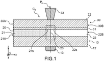
- resistive C 1 memory cell structure An example of resistive C 1 memory cell structure according to an embodiment of the present invention is given on the figure 1 .
- the resistive and non-volatile memory cell C 1 belongs to a memory matrix which is typically provided with a plurality of cells (not shown).
- the memory array is formed in thin layers on a support (not shown) such as a semiconductor substrate or a semiconductor-on-insulator type substrate.
- the memory matrix can be integrated into a lower stage of a microelectronic device and carried out in particular during so-called “FEOL” type steps for (“Front End-Of-Line”), that is to say at the beginning of a process for manufacturing the microelectronic device, the stage then being located at the level of the transistors.
- the memory array can be integrated above a metal interconnection level or between metal interconnection levels, during MEOL (for “Middle-End-Of-Line”) or of the type BEOL (for “Back-End-Of-Line”).
- the memory cells can be integrated for example between a fifth stage ("metal 5") of connection lines and a sixth stage ("metal 6") of connection lines or between a fourth stage ("metal 4") and a fifth stage ("metal 5").
- the resistive memory cell C 1 comprises a first electrode 10, a second electrode 30 and a layer 20 of dielectric material placed between the first electrode 10 and the second electrode 30.
- the first electrode 10 is, in this example, called the “lower” electrode.
- the second electrode 30 is called the “upper” electrode, the terms “lower” and “upper” being used here to characterize the position of the electrodes in the reference frame of the figures.
- the memory cell C 1 has, just like a conventional resistive memory cell, an operation allowing it to reversibly switch between two resistance states as a function of the voltage applied to its electrodes 10, 30.
- the memory cell C 1 is thus able to switch reversibly between a so-called “high resistance” state and a so-called “low resistance” state.
- the dielectric layer 20 comprises a so-called “switching" zone in which a privileged current conduction path called a conductive filament is likely to be created when an appropriate voltage is applied to the electrodes 10, 30.
- the memory cell C 1 is located then in a state of low resistance, a state in which a current for example comprised between 5 ⁇ A and 25 ⁇ A is likely to pass through it.
- Cell C 1 finds itself in a high resistance state with a lower current, for example less than 10 ⁇ A, than in the low resistance state and for example comprised between 1 ⁇ A and 10 ⁇ A.
- the read current which passes through the cell when it is read depends on the read voltage applied, the read voltage being, for the current values given above, typically between 0.05V and 0.4V.
- the electrodes 10, 30 are each formed of one or more conductive layers and can comprise one or more conductive materials such as titanium nitride, titanium, tungsten. At least one of the electrodes, in this example the upper electrode 30, is provided with a layer 31 of oxygen sensor material (“oxygen scavenger” according to the English terminology) in other words having a strong affinity with oxygen such as for example titanium (Ti), tantalum (Ta), or hafnium (Hf). This layer 31 is here placed in contact with the dielectric layer 20 . Electrodes 10, 30 are typically formed by layers 12, 32 of conductive material which can also be a metal diffusion barrier towards the dielectric layer such as TaN or TiN. In this example, conductive contacts 13, 33 made of metal, for example such as tungsten, are also provided.
- oxygen sensor material oxygen scavenger
- the layer of dielectric material 20 can be a layer based on oxide or containing oxide regions, preferably a transition metal oxide, for example such as a hafnium oxide HfO 2 or HfOx, or a tantalum Ta 2 O 5 or Ta x O y , or a tungsten oxide WOx.
- the oxide layer 20 can also be based on or include silicon oxide.
- the layer of dielectric material 20 may comprise several superposed oxide sub-layers.
- the layer 20 of dielectric material can be provided with a thickness comprised for example between 3 nm and 20 nm, and preferably between 5 nm and 10 nm.
- the inventors Rather than establishing a switching zone at the center of a doped region of the dielectric layer in which charges have been created, the inventors have discovered, surprisingly, that a spatial confinement of the conductive filament could be obtained at the level of an interface zone 23 between adjoining dielectric regions 21, 22 of different compositions, in particular in terms of doping and/or constant dielectric.
- the cell C 1 therefore has here the particularity of having a switching zone, in other words a conductive filament formation zone, which is located at an interface 23 between two distinct dielectric regions 21, 22 and in contact with one of the 'other.
- These regions 21, 22 distinct from the layer of dielectric material 20 can be regions of the same dielectric material but with different respective dopings or else consist of different dielectric materials with different respective dielectric constants.
- a first region 21 of the dielectric layer 20 comprises a doping element, typically silicon or aluminum, according to an atomic concentration of doping element or a given density of doping element, while that a second region 22 of the dielectric layer 20 is undoped or is also doped but with an atomic concentration of said doping element lower than in the first region 21.
- a doping element typically silicon or aluminum
- the first region 21 is an oxide region, in particular a transition metal oxide doped with silicon, it is possible to provide an atomic concentration of doping element between 0.1% and 5%, advantageously between 0.3% and 2%, and of preferably between 0.5% and 1.5%.
- first region 21 and the second region 22 are both doped with silicon, a difference in concentration preferably greater than 0.3% can be provided.
- the first region 21 is an oxide region doped with aluminum
- an atomic concentration of doping element preferably greater than 1%, for example between 1% and 5%.
- a difference in concentration preferably greater than 0.3% can be provided.
- composition of the dielectric layer 20 provides a first region 21 based on hafnium oxide doped with silicon (HfO 2 :Si) or aluminum, while the second region 22 is made of hafnium oxide. undoped hafnium or with a concentration of dopants, in particular silicon or aluminum, lower than that of the first region 21.
- the first region 21 can be based on tantalum oxide (Ta 2 O 5 :Si, TaO x :Si) doped with silicon while the second region 22 is in undoped tantalum oxide or with a silicon concentration lower than that of the first region 21.
- tantalum oxide Ti 2 O 5 :Si, TaO x :Si
- a third example of composition provides a first region 21 in silicon oxide doped with hafnium while the second region 22 is in undoped silicon oxide or doped for example with hafnium and comprising a hafnium concentration lower than that of the first region 21.
- the regions 21, 22 can be regions of the same transition metal oxide, but doped with different species.
- a particular embodiment provides a first region 21 based on hafnium oxide doped with silicon, while the second region 22 is made of hafnium oxide doped with aluminum.
- the regions 21, 22 can be regions based on different dielectric materials and having different dielectric constants.
- a particular embodiment of this variant provides the second region 22 in a dielectric material of the type commonly called “high-k”, in other words with a dielectric constant greater than that of silicon oxide, in particular a metal oxide of transition, for example hafnium oxide, and the first region 21 based on another dielectric material, for example SiO 2 or silicon nitride (Si x N y ), a dielectric material of the type commonly called " low-k” (dielectric constant lower than that of silicon oxide).
- the electrodes 10, 30 are arranged facing this interface 23.
- the interface 23 extends in a plane P m crossing the dielectric layer 20 and passing through the electrodes 10, 30.
- the plane P m in which the interface 23 extends can form a median plane of the upper 10 and/or lower 30 electrode.
- vertical plane is meant a plane which extends parallel to the z axis of the orthogonal frame [O; x; y; z] given on the figure 1 .
- the arrangement of the regions 21, 22 facing the electrodes may be such that the first dielectric region 21 extends in a direction parallel to a main plane of the dielectric layer 20, from said interface 23 at least to a zone 21A located facing a first side face 30A delimiting at least one of the electrodes 20, 30 here from the upper electrode 30.
- the second dielectric region 22 extends, for its part, in a direction parallel to a main plane of the dielectric layer 20 between said interface 23 and a zone 22B in the extension of a second side face 30B delimiting said upper electrode 30 and which is opposite said first side face 30A.
- main plane of the dielectric layer 20 is meant a plane passing through this dielectric layer 20 and which extends along this dielectric layer 20 parallel to the plane [O; x; y] of the orthogonal coordinate system [O; x; y; z] given on the figure 1 .
- the arrangement of the dielectric regions 21, 22 can advantageously be provided as in the example illustrated in the figure 1 with a single interface 23 between regions 21, 22 of different compositions, the cell C 1 then comprising a single switching zone facing the upper electrode 30. This can make it possible to reduce the electrical consumption and the level of the read voltages, writing, erasing applied with respect to a cell in which there would be several switching zones facing the same electrode 30.
- At least one of the electrodes is centered opposite the interface zone 23, which makes it possible to further promote the confinement of the conductive filament at the level of the interface 23 between the regions 21, 22.
- at least one of the electrodes, in this example the upper electrode 30, extends facing a surface 21s of the first region 21 equal or substantially equal to a surface 22s of the second region 22 facing which it extends.
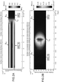
- the Figures 2A-2B give simulation results obtained using the COMSOL Multiphysics tool respectively on an axial component and a radial component of the electric field in the dielectric layer of a cell structure of the type described previously.
- the electrodes are in particular arranged facing an interface between a first region R 21 of hafnium oxide doped with silicon and a second region R 22 of undoped hafnium oxide.
- the greater radial component of the electric field at the level of the interface I 23 between the uncharged region and which is not doped with silicon and the charged region shows that a greater current density is obtained at the level of this interface I 23 and, therefore, a confinement effect of the conductive filament is obtained.
- the Figures 5A, 5B, 5C each give curves of simulation results giving the evolution of a maximum radial electric field in a cell structure as described above as a function of the dielectric constant ratio between the first dielectric region, which is doped here, and the second region which is not doped.
- the first region (curve 510) has a dielectric constant which varies to approximate the behavior of a low-k dielectric, while the second region (curve 520) joined to the first region is made of undoped hafnium oxide of dielectric constant equal to 19.
- the first region (curve 530) is made of silicon-doped hafnium oxide with a dielectric constant of the order of 18.25, while the second region (curve 530) has a dielectric constant which varies to approximate the behavior of a low-k dielectric.
- the first region 550 has a dielectric constant which varies to approach the behavior of a low-k dielectric, while a second region 560 attached to the first region is provided with a dielectric constant of 3.9.
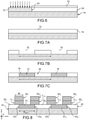
- FIG. 6 A particular way of manufacturing a memory cell interface 23 as described previously formed of regions 21, 22 juxtaposed and in contact with one another is illustrated in the figure 6 .
- the first region 21 is doped using one implantation or several successive implantations.
- the implantation or implantations are carried out in a dielectric layer 20, while a second region 22 of this layer 20 is preserved during this implantation, typically by means of a mask 61 arranged on the second region 22.
- an implantation carried out at an energy of 4 keV, with a dose of between 1 ⁇ 10 15 atoms ⁇ cm-2 and 5 ⁇ 10 15 atoms ⁇ cm-2 can be performed. Then, the mask 61 is removed.
- the upper electrode is then made opposite the interface 23 between the implanted region and the non-implanted region, and possibly centered opposite this interface 23.
- FIG. 7A After deposit ( Figure 7A ) of a layer 70 of a first dielectric material 72, for example silicon nitride, one or more openings 75 are formed in this layer 70 by revealing the lower electrode 10 ( figure 7B ).
- a first dielectric material 72 for example silicon nitride
- the openings 75 can be made using a photolithography process during which a masking (not shown) is formed and through which the dielectric layer 70 is etched.
- CMP planarization for "Chemical Mechanical Planarization"
- CMP planarization can then be carried out in order to obtain a flat layer comprising at least one region 21 made of a dielectric material attached to another region of dielectric material 22 with a dielectric constant different from that of the first material.
- the memory matrix is here provided with upper electrodes 30 1 , 30 2 , 30 3 , 30 4 which are distinct and which may not be connected to each other. These upper electrodes 30 1 , 30 2 , 30 3 , 30 4 are arranged facing respectively interfaces 23 1 , 23 2 , 23 3 , 23 4 between adjoining dielectric regions having different respective dielectric constants and/or concentrations of different doping element.
- the respective switching zones of the cells C 11 , C 12 , C 13 , C 14 are thus also placed at the level of the interfaces 23 1 , 23 2 , 23 3 , 23 4 .
- the dielectric layer 20 this time comprises an alternation of regions 21 1 , 21 2 , of a first type having a composition which may be similar to that of the first region 21 of the structure described previously in connection with the figure 1 , and regions 22 1 , 22 2 , 22 3 , of a second type, of different composition and dielectric constant from the first region.
- the regions 22 1 , 22 2 , 22 3 can have a composition similar to that of the second region 22 previously described in connection with the figure 1 .
- the regions 22 1 , 22 2 , 22 3 are for example non-doped regions of a layer of hafnium oxide, while the regions 21 1 , 21 2 are for example regions implanted with silicon in this hafnium oxide layer.
- An upper electrode 30 1 and another upper electrode 30 2 are here arranged partially facing the same dielectric region 21 1 of the first type, for example of doped transition metal oxide, and partially facing two dielectric regions 22 1 , 22 1 of the second type, while being placed opposite interfaces 23 1 , 23 2 distinct.
- the electrodes 30 1 , 30 2 can therefore make it possible to supply separate switching zones.
- another upper electrode 30 3 and the upper electrode 30 2 are placed partly overlapping on the same dielectric region 22 2 , for example of undoped transition metal oxide, while being placed opposite separate interfaces 23 2 , 23 3 and separate switching zones.
- Such arrangements make it possible in particular to be able to produce memories of small dimensions while having reduced constraints concerning their dimensioning, in particular as regards the pitch p mem of distribution of the cells C 11 , C 12 , C 13 , C 14 memories as well as the width W of the electrodes. For equal cell size, it is possible to obtain a pitch twice as large while having an increased electrode width W compared to a device according to the prior art.
- the fact of providing electrodes of greater width W can make it possible to relax the misalignment tolerance constraints between a given level of the microelectronic device in which the memory cells C 11 , C 12 , C 13 , C 14 are formed and a level higher and/or lower than the given level. This can also make it easier to make contact on the electrodes and make the design of the cells easier in terms of layout constraints.
- the upper electrodes 30 1 , 30 2 , 30 3 , 30 4 can be centered opposite the zones 23 1 , 23 2 , 23 3 , 23 4 respectively. It is also possible to provide a single switching zone per cell, so that two separate upper electrodes 30 1 , 30 2 make it possible to control two separate switching zones of two separate cells.
- a single lower electrode 10 1 is shown but the device can also be provided with additional lower electrodes (not shown) typically parallel to each other.
- the lower and upper electrodes here have different respective orientations.
- the memory follows an arrangement of the so-called “crossbar” type.
- the upper electrodes 30 1 , 30 2 , 30 3 , 30 4 thus extend parallel to a given direction, in this example parallel to the axis y of the reference [O; x; y; z], while the lower electrode or electrodes 10 1 extend parallel to another direction, orthogonal to said given direction and in this example parallel to the x axis.
- the upper electrodes 30 1 , 30 2 , 30 3 , 30 4 whose orientation follows that of the interface zones 23 1 , 23 2 , 23 3 , 23 4 , but it is also possible to provide an inverse arrangement where the lower electrodes 10 1 , 10 2 , 10 3 , 10 4 are oriented in a direction parallel to that in which the interface zones 23 1 , 23 2 , 23 3 , 23 4 , the upper electrodes then being orthogonal to the lower electrodes.
- the upper electrodes 30 1 , 30 2 , 30 3 , 30 4 , and the lower electrodes 10 1 , 10 2 , 10 3 , 10 4 , of the resistive memory cells follow the same orientation.
- Each pair of upper and lower electrodes is distributed here symmetrically on either side of a block 90 of dielectric material comprising an interface 23 between a dielectric region 21 and an adjoining dielectric region 22 of different dielectric constant and/or of different doping.
- the pairs of electrodes 10 1 , 30 1 , 10 2 , 30 2 ,..., are here separated from each other by trenches filled with insulating material 92, for example silicon nitride SiN or SiO 2 .
- a memory device As described above, it is possible to start from a support formed from a substrate, of the solid type (bulk) or of the semiconductor-on-insulator type, for example SOI, on which at least one stage of transistors is produced. .
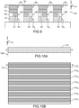
- a particular embodiment illustrated on the Figures 10A-10F plans to manufacture the memory device during a set of back-end steps above the level of the transistors and at least one stage of already formed connection elements.
- the parallel conductive lines 110 1 ,... 110 7 can be formed by etching or else by filling trenches. Insulating areas 113, for example made of silicon oxide, are provided between the conductive lines.
- At least one layer 120 of dielectric material such as for example hafnium oxide or tantalum oxide is deposited with a thickness which can be for example between 3 nm and 25 nm.
- doped regions 121 are produced in this oxide layer 120 by carrying out one or more successive implantations.
- the layer of dielectric material 120 is a layer of transition metal oxide such as hafnium oxide or tantalum oxide
- an implantation of silicon or aluminum can be carried out.
- implantation is performed through openings 124 of a mask 125, which is then removed.
- the openings 124 of the mask 125 can be in the form of oblong trenches, for example rectangular, so as to produce doped regions 121 of corresponding shape.
- the doped regions 121 can be distributed in a regular manner according to a pitch p dop twice as high as that of the memory points.
- the distribution pitch of the memory points can correspond to that of the interfaces between doped regions 121 and non-doped regions 122.
- a conductive stack is produced provided with a layer 131 of oxygen-sensing material, for example based on Ti, and with a thickness which may for example be between 3 nm and 20 nm.
- the stack also includes a layer 132 of conductive material, for example TiN, deposited on the oxygen-sensing material and with a thickness which can be for example between 5 nm. 300nm.
- the etching of the layers 131, 132 to form the upper electrode 130, in particular of the layer of oxygen sensor material, typically based on Ti, can, as illustrated in the figure 11 , lead to formation of zones oxidized 135 at the side flanks of the electrodes 130 1 , 130 2 , 130 3 , 130 4 .
- the impact of such oxidized zones 135 on the operation of the cells is less insofar as the switching zone is here provided at the level of the interface 123, otherwise said at a distance from oxidized areas 135.
- an anisotropic etching is carried out to produce the upper electrodes 130 which are then continued in the layer of dielectric material 120 and in the layer or layers forming the lower electrode or electrodes.
- Such an arrangement with a dielectric layer etched into separate blocks 90 each equipped with an interface 123 does not, again, disturb the operation of the switching zone insofar as the latter is located at a distance from the side flanks 90A, 90B of blocks 90.
- the doped regions 121 can be produced in several steps by successive implantations, respectively through openings of a masking which are oriented in a first direction, then through other openings of another masking which are oriented in a second direction orthogonal to the first direction.
Landscapes
- Engineering & Computer Science (AREA)
- Manufacturing & Machinery (AREA)
- Semiconductor Memories (AREA)
Applications Claiming Priority (1)
| Application Number | Priority Date | Filing Date | Title |
|---|---|---|---|
| FR2008916A FR3113783B1 (fr) | 2020-09-02 | 2020-09-02 | Memoire resistive a zone de commutation entre deux regions dielectriques de dopages et/ou constantes dielectriques different(e)s |
Publications (1)
| Publication Number | Publication Date |
|---|---|
| EP3965177A1 true EP3965177A1 (de) | 2022-03-09 |
Family
ID=74045604
Family Applications (1)
| Application Number | Title | Priority Date | Filing Date |
|---|---|---|---|
| EP21192810.6A Pending EP3965177A1 (de) | 2020-09-02 | 2021-08-24 | Resistiver speicher mit einer schaltzone zwischen zwei dielektrischen bereichen mit unterschiedlichen dotierungen und/oder dielektrizitätskonstanten |
Country Status (3)
| Country | Link |
|---|---|
| US (1) | US11944022B2 (de) |
| EP (1) | EP3965177A1 (de) |
| FR (1) | FR3113783B1 (de) |
Families Citing this family (1)
| Publication number | Priority date | Publication date | Assignee | Title |
|---|---|---|---|---|
| US12557314B2 (en) * | 2022-08-03 | 2026-02-17 | Taiwan Semiconductor Manufacturing Co., Ltd. | Gate-all-around field-effect transistor device |
Citations (5)
| Publication number | Priority date | Publication date | Assignee | Title |
|---|---|---|---|---|
| US20090014710A1 (en) * | 2006-03-08 | 2009-01-15 | Yoshio Kawashima | Nonvolatile memory element, nonvolatile memory apparatus, and method of manufacture thereof |
| US20100243983A1 (en) | 2009-03-31 | 2010-09-30 | Tony Chiang | Controlled localized defect paths for resistive memories |
| US20100314602A1 (en) * | 2009-06-10 | 2010-12-16 | Kensuke Takano | Nonvolatile memory device and method for manufacturing same |
| US20120063201A1 (en) * | 2010-03-19 | 2012-03-15 | Yukio Hayakawa | Nonvolatile memory element, production method therefor, design support method therefor, and nonvolatile memory device |
| FR2995443A1 (fr) * | 2012-09-10 | 2014-03-14 | St Microelectronics Crolles 2 | Cellule memoire a changement de phase |
Family Cites Families (1)
| Publication number | Priority date | Publication date | Assignee | Title |
|---|---|---|---|---|
| WO2011013255A1 (ja) * | 2009-07-31 | 2011-02-03 | 株式会社 東芝 | 不揮発性記憶装置 |
-
2020
- 2020-09-02 FR FR2008916A patent/FR3113783B1/fr active Active
-
2021
- 2021-08-24 EP EP21192810.6A patent/EP3965177A1/de active Pending
- 2021-08-30 US US17/446,328 patent/US11944022B2/en active Active
Patent Citations (5)
| Publication number | Priority date | Publication date | Assignee | Title |
|---|---|---|---|---|
| US20090014710A1 (en) * | 2006-03-08 | 2009-01-15 | Yoshio Kawashima | Nonvolatile memory element, nonvolatile memory apparatus, and method of manufacture thereof |
| US20100243983A1 (en) | 2009-03-31 | 2010-09-30 | Tony Chiang | Controlled localized defect paths for resistive memories |
| US20100314602A1 (en) * | 2009-06-10 | 2010-12-16 | Kensuke Takano | Nonvolatile memory device and method for manufacturing same |
| US20120063201A1 (en) * | 2010-03-19 | 2012-03-15 | Yukio Hayakawa | Nonvolatile memory element, production method therefor, design support method therefor, and nonvolatile memory device |
| FR2995443A1 (fr) * | 2012-09-10 | 2014-03-14 | St Microelectronics Crolles 2 | Cellule memoire a changement de phase |
Non-Patent Citations (1)
| Title |
|---|
| HAYAKAWA Y. ET AL.: "Highly reliable TaOx ReRAM with centralized filament for 28-nm embedded application", SYMPOSIUM ON VLSI TECHNOLOGY, KYOTO, 2015, XP033211427, ISSN: 0743-1562, DOI: 10.1109/VLSIT.2015.7223684 |
Also Published As
| Publication number | Publication date |
|---|---|
| US20220069217A1 (en) | 2022-03-03 |
| FR3113783B1 (fr) | 2022-08-12 |
| FR3113783A1 (fr) | 2022-03-04 |
| US11944022B2 (en) | 2024-03-26 |
Similar Documents
| Publication | Publication Date | Title |
|---|---|---|
| US7405418B2 (en) | Memory device electrode with a surface structure | |
| US8198144B2 (en) | Pillar structure for memory device and method | |
| US8471235B2 (en) | Nonvolatile memory element having a resistance variable layer and manufacturing method thereof | |
| CN101685827A (zh) | 一种存储装置及其制造方法 | |
| US9159917B2 (en) | Nonvolatile memory element and method of manufacturing nonvolatile memory element | |
| EP3750199B1 (de) | Dreidimensionaler widerstandsspeicher | |
| EP3542406B1 (de) | Verfahren zur herstellung eines resistiven speichers | |
| EP4175448B1 (de) | Verfahren zur co-herstellung eines ferroelektrischen speichers und eines resistiven oxram-speichers und vorrichtung mit einem ferroelektrischen speicher und einem resistiven oxram-speicher | |
| EP1801897B1 (de) | Verbessertes Verfahren zur Herstellung von Speicherzellen vom Typ PMC | |
| EP3510644B1 (de) | Oxidbasierte resistive nichtflüchtige speicherzelle und verfahren zur herstellung davon | |
| EP3965177A1 (de) | Resistiver speicher mit einer schaltzone zwischen zwei dielektrischen bereichen mit unterschiedlichen dotierungen und/oder dielektrizitätskonstanten | |
| US9673255B2 (en) | Resistive memory device and fabrication methods | |
| EP3843143B1 (de) | 3d-speicher und dessen herstellungsverfahren | |
| EP4454443B1 (de) | Anordnung mit mindestens zwei nichtflüchtigen resistiven speichern und zwei selektoren, matrix und zugehöriges herstellungsverfahren | |
| EP4550968B1 (de) | Speichervorrichtung mit rram-speicherzellen mit optimierter aktiver oberfläche | |
| EP4454444B1 (de) | Anordnung mit mindestens zwei nichtflüchtigen resistiven speichern und einem selektor, matrix und zugehöriges herstellungsverfahren | |
| EP4572594A1 (de) | Nichtflüchtige speicherstruktur mit einem stapel angeordnet in einem via und einer leitung darüber | |
| EP3404730A1 (de) | Nicht-flüchtiger speicher, der eine grosse integrationsdichte begünstigt | |
| EP4576980A1 (de) | Ferroelektrische speicheranordnung und verfahren zu ihrer herstellung | |
| EP4576985A1 (de) | Ferroelektrische speicheranordnung und verfahren zur herstellung einer solchen | |
| EP4576984A1 (de) | Ferroelektrische speicheranordnung und verfahren zu ihrer herstellung | |
| FR3131438A1 (fr) | Ensemble comprenant au moins deux sélecteurs et deux mémoires résistives non-volatiles, matrice et procédé de fabrication associés | |
| FR3157056A1 (fr) | Procédé de fabrication d’un cellule mémoire résistive de type OxRAM et cellule mémoire de type OxRAM associée | |
| FR3044823A1 (fr) | Dispositif a transistors repartis sur plusieurs niveaux superposes integrant une memoire resistive | |
| FR3151734A1 (fr) | Cellule mémoire résistive de type OxRAM et procédé de fabrication associé |
Legal Events
| Date | Code | Title | Description |
|---|---|---|---|
| PUAI | Public reference made under article 153(3) epc to a published international application that has entered the european phase |
Free format text: ORIGINAL CODE: 0009012 |
|
| STAA | Information on the status of an ep patent application or granted ep patent |
Free format text: STATUS: REQUEST FOR EXAMINATION WAS MADE |
|
| 17P | Request for examination filed |
Effective date: 20210824 |
|
| AK | Designated contracting states |
Kind code of ref document: A1 Designated state(s): AL AT BE BG CH CY CZ DE DK EE ES FI FR GB GR HR HU IE IS IT LI LT LU LV MC MK MT NL NO PL PT RO RS SE SI SK SM TR |
|
| RAP3 | Party data changed (applicant data changed or rights of an application transferred) |
Owner name: COMMISSARIAT A L'ENERGIE ATOMIQUE ET AUX ENERGIESALTERNATIVES |