EP3510644B1 - Oxidbasierte resistive nichtflüchtige speicherzelle und verfahren zur herstellung davon - Google Patents
Oxidbasierte resistive nichtflüchtige speicherzelle und verfahren zur herstellung davon Download PDFInfo
- Publication number
- EP3510644B1 EP3510644B1 EP17768728.2A EP17768728A EP3510644B1 EP 3510644 B1 EP3510644 B1 EP 3510644B1 EP 17768728 A EP17768728 A EP 17768728A EP 3510644 B1 EP3510644 B1 EP 3510644B1
- Authority
- EP
- European Patent Office
- Prior art keywords
- zone
- memory cell
- oxide layer
- electrode
- silicon
- Prior art date
- Legal status (The legal status is an assumption and is not a legal conclusion. Google has not performed a legal analysis and makes no representation as to the accuracy of the status listed.)
- Active
Links
Images



Classifications
-
- H—ELECTRICITY
- H10—SEMICONDUCTOR DEVICES; ELECTRIC SOLID-STATE DEVICES NOT OTHERWISE PROVIDED FOR
- H10B—ELECTRONIC MEMORY DEVICES
- H10B63/00—Resistance change memory devices, e.g. resistive RAM [ReRAM] devices
- H10B63/80—Arrangements comprising multiple bistable or multi-stable switching components of the same type on a plane parallel to the substrate, e.g. cross-point arrays
-
- H—ELECTRICITY
- H10—SEMICONDUCTOR DEVICES; ELECTRIC SOLID-STATE DEVICES NOT OTHERWISE PROVIDED FOR
- H10B—ELECTRONIC MEMORY DEVICES
- H10B63/00—Resistance change memory devices, e.g. resistive RAM [ReRAM] devices
- H10B63/80—Arrangements comprising multiple bistable or multi-stable switching components of the same type on a plane parallel to the substrate, e.g. cross-point arrays
- H10B63/82—Arrangements comprising multiple bistable or multi-stable switching components of the same type on a plane parallel to the substrate, e.g. cross-point arrays the switching components having a common active material layer
-
- H—ELECTRICITY
- H10—SEMICONDUCTOR DEVICES; ELECTRIC SOLID-STATE DEVICES NOT OTHERWISE PROVIDED FOR
- H10N—ELECTRIC SOLID-STATE DEVICES NOT OTHERWISE PROVIDED FOR
- H10N70/00—Solid-state devices having no potential barriers, and specially adapted for rectifying, amplifying, oscillating or switching
- H10N70/011—Manufacture or treatment of multistable switching devices
- H10N70/041—Modification of switching materials after formation, e.g. doping
- H10N70/043—Modification of switching materials after formation, e.g. doping by implantation
-
- H—ELECTRICITY
- H10—SEMICONDUCTOR DEVICES; ELECTRIC SOLID-STATE DEVICES NOT OTHERWISE PROVIDED FOR
- H10N—ELECTRIC SOLID-STATE DEVICES NOT OTHERWISE PROVIDED FOR
- H10N70/00—Solid-state devices having no potential barriers, and specially adapted for rectifying, amplifying, oscillating or switching
- H10N70/20—Multistable switching devices, e.g. memristors
- H10N70/24—Multistable switching devices, e.g. memristors based on migration or redistribution of ionic species, e.g. anions, vacancies
-
- H—ELECTRICITY
- H10—SEMICONDUCTOR DEVICES; ELECTRIC SOLID-STATE DEVICES NOT OTHERWISE PROVIDED FOR
- H10N—ELECTRIC SOLID-STATE DEVICES NOT OTHERWISE PROVIDED FOR
- H10N70/00—Solid-state devices having no potential barriers, and specially adapted for rectifying, amplifying, oscillating or switching
- H10N70/20—Multistable switching devices, e.g. memristors
- H10N70/24—Multistable switching devices, e.g. memristors based on migration or redistribution of ionic species, e.g. anions, vacancies
- H10N70/245—Multistable switching devices, e.g. memristors based on migration or redistribution of ionic species, e.g. anions, vacancies the species being metal cations, e.g. programmable metallization cells
-
- H—ELECTRICITY
- H10—SEMICONDUCTOR DEVICES; ELECTRIC SOLID-STATE DEVICES NOT OTHERWISE PROVIDED FOR
- H10N—ELECTRIC SOLID-STATE DEVICES NOT OTHERWISE PROVIDED FOR
- H10N70/00—Solid-state devices having no potential barriers, and specially adapted for rectifying, amplifying, oscillating or switching
- H10N70/801—Constructional details of multistable switching devices
- H10N70/821—Device geometry
- H10N70/826—Device geometry adapted for essentially vertical current flow, e.g. sandwich or pillar type devices
-
- H—ELECTRICITY
- H10—SEMICONDUCTOR DEVICES; ELECTRIC SOLID-STATE DEVICES NOT OTHERWISE PROVIDED FOR
- H10N—ELECTRIC SOLID-STATE DEVICES NOT OTHERWISE PROVIDED FOR
- H10N70/00—Solid-state devices having no potential barriers, and specially adapted for rectifying, amplifying, oscillating or switching
- H10N70/801—Constructional details of multistable switching devices
- H10N70/821—Device geometry
- H10N70/828—Current flow limiting means within the switching material region, e.g. constrictions
-
- H—ELECTRICITY
- H10—SEMICONDUCTOR DEVICES; ELECTRIC SOLID-STATE DEVICES NOT OTHERWISE PROVIDED FOR
- H10N—ELECTRIC SOLID-STATE DEVICES NOT OTHERWISE PROVIDED FOR
- H10N70/00—Solid-state devices having no potential barriers, and specially adapted for rectifying, amplifying, oscillating or switching
- H10N70/801—Constructional details of multistable switching devices
- H10N70/841—Electrodes
-
- H—ELECTRICITY
- H10—SEMICONDUCTOR DEVICES; ELECTRIC SOLID-STATE DEVICES NOT OTHERWISE PROVIDED FOR
- H10N—ELECTRIC SOLID-STATE DEVICES NOT OTHERWISE PROVIDED FOR
- H10N70/00—Solid-state devices having no potential barriers, and specially adapted for rectifying, amplifying, oscillating or switching
- H10N70/801—Constructional details of multistable switching devices
- H10N70/881—Switching materials
- H10N70/883—Oxides or nitrides
- H10N70/8833—Binary metal oxides, e.g. TaOx
Definitions
- the technical field of the invention is that of non-volatile memories, and more particularly that of resistive memories based on oxide.
- Resistive memories are non-volatile memories but which have sufficiently high operating speeds to claim to replace both random access memories and current non-volatile memories such as flash-type memories.
- Resistive memories are based on an active material that can switch reversibly between two states of resistance which make it possible to encode a bit of information.
- resistive memories for which the active material is based on oxide. This is particularly the case of memories of the OxRAM type, for “Oxide resistive Random Access Memory” in English, and of certain memories of the CBRAM type, for “Conductive Bridging Random Access Memory” in English.
- Oxide-based resistive memories have a high integration density and are compatible with CMOS technology manufacturing processes. Oxide-based resistive memories can be integrated both at the end of the manufacturing line, what is called BEOL for "Back-End-Of-Line” in English, and at the start of the manufacturing line, which we call FEOL for “Front-End-Of-Line” in English.
- a resistive memory based on oxide comprises a multitude of memory cells arranged in rows and in columns to form a matrix. Each memory cell has an oxide layer placed between two electrodes. The oxide layer switches reversibly between two resistance states depending on the voltage applied to the memory cell. A write voltage is used to transition the oxide layer to a low resistance state, while an erase voltage is used to transition the oxide layer to a high resistance state.
- the change of resistance state is linked to the formation and rupture, in the oxide layer, of a switching zone, also called "switching". zone” in English, which forms an electrically conductive path connecting the electrodes of the memory cell.
- switching zone in English, which forms an electrically conductive path connecting the electrodes of the memory cell.
- the conductive path is a filament formed by metal ions
- OxRAM memories the formation of the conductive path is attributed to the accumulation of oxygen vacancies within the oxide layer. .
- the resistance states each have a discrete value but in practice the resistance states each span a range of values.
- the resistance states may therefore overlap, making it difficult to distinguish between the low resistance state and the high resistance state. In order to avoid this, it may therefore be necessary to increase the size of the cell memory window, i.e. the difference between the resistance values defining the low-resistance state and the low-resistance state. strong resistance.
- the present invention aims to provide a resistive non-volatile memory cell based on oxide in which the location of the filament is controlled in a simple manner, the memory cell thus exhibiting lower variability.
- a forming voltage also called “forming voltage”
- forming voltage is applied to the memory cell in order to form the switching zone for the first time. It has been found that by appropriately doping the first area with aluminum or silicon, to form the switching area in the first doped area, it is necessary to apply to the memory cell a first forming voltage greater than a reference formation voltage that must be applied to form the switching zone in the undoped oxide layer. In other words, by keeping the formation voltage lower than the first formation voltage, the switching zone forms where the oxide layer is not doped. Thanks to the invention, it is therefore possible to control in a simple manner the location of the switching zone by suitable doping of the oxide layer, which thus makes it possible to reduce the variability of the memory cells.
- the memory cell comprises a first electrode 1, a second electrode 2 and an oxide layer 3 placed between the first electrode 1 and the second electrode 2.
- the first electrode 1 is for example placed on a substrate (not shown), the first electrode 1 being designated as the lower electrode.
- the second electrode 2 is then designated as the upper electrode.
- the terms “lower” and “upper” are used to characterize the position of the electrodes in the frame of reference of the substrate.
- the substrate is for example made of silicon and may include other layers already formed on it.
- the electrodes 1, 2 are electrically conductive layers and may comprise one or more conductive materials such as titanium nitride, doped silicon, tungsten, tungsten nitride, metal silicides, platinum.
- the electrodes 1, 2 have a thickness preferably between 5 nm and 30 nm.
- the oxide layer 3 preferably comprises an oxide of a transition metal such as hafnium oxide, tantalum oxide, titanium oxide, nickel oxide, tungsten oxide or 'zinc oxide.
- the oxide layer 3 can also comprise silicon oxide, aluminum oxide, indium oxide or gadolinium oxide.
- the oxide layer 3 may comprise several superposed oxide sub-layers.
- the oxide layer 3 has a thickness preferably between 3 nm and 20 nm, and more preferably still between 5 nm and 10 nm.
- the memory cell is an oxide-based memory cell whose operation is as follows.
- the oxide layer 3 and more generally the memory cell, can switch reversibly between two resistance states. When a voltage is applied to the memory cell, the latter is traversed by a current of greater or lesser intensity depending on the state of resistance in which the memory cell is located.
- a write voltage is applied to the memory cell to form a switching zone in the oxide layer 3, between the electrodes 1, 2.
- the memory cell thus passes into a state low resistance, also called LRS for “Low Resistance State” in English.
- LRS Low Resistance State
- the current passing through the memory cell is considered to be of high intensity, and this current passes mainly through the switching zone which has a lower resistance than the rest of the oxide layer 3.
- an erase voltage is applied to the memory cell to break the switching region.
- the memory cell thus passes into a high resistance state, also called HRS for “High Resistance State”. In this state, the current passing through the memory cell is considered to be of low intensity.
- the switching zone is formed for the first time by applying to the memory cell a formation voltage higher than the write voltage. Then the memory cell enters a normal operating mode in which the write voltage and the erase voltage are used to toggle the resistance state of the memory cell.
- the switching zone Once the switching zone has formed for the first time at a location of the oxide layer 3, it always reforms at this location during subsequent write operations.
- the resistance state in which the memory cell is located can be determined by applying a read voltage to it.
- the memory cell may comprise a layer 9 formed with a material having a high affinity for oxygen, this layer thus forming a reservoir of oxygen vacancies which facilitates the formation of the switching zone by providing the necessary vacancies.
- the reservoir layer 9 is for example placed between the oxide layer 3 and the upper electrode 2.
- the reservoir layer has a thickness preferably between 2 nm and 10 nm, and more preferably still between 3 nm and 7 nm.
- the reservoir layer 9 comprises for example titanium, zirconium, hafnium or lanthanum.
- the present invention is based on the observation that, when the oxide layer 3 is doped with aluminum or silicon, the formation voltage of the switching zone in the oxide layer 3 varies according to the atomic concentration of aluminum or silicon in the oxide layer 3.
- the term “doping element” refers indiscriminately to aluminum or to silicon.
- the formation voltage when the atomic concentration of the doping element is zero, that is to say when the oxide layer 3 is not doped, is taken as the reference voltage.
- the oxide layer 3 is doped with silicon
- the formation voltage begins by increasing with the atomic concentration of silicon until it reaches a maximum value. Then, when the silicon atomic concentration continues to increase, the formation voltage decreases, passing below the reference voltage.
- the oxide layer 3 is doped with aluminum
- the formation voltage increases linearly with the aluminum atomic concentration.
- the memory cells are memory cells of the OxRAM type in which the electrodes 1, 2 are made of titanium nitride, the oxide layer 3 is made of hafnium oxide and the reservoir layer 9 is titanium. Furthermore, the oxide layer 3 comprises a first zone 31 doped with aluminum or silicon in which the atomic concentration of aluminum or silicon is chosen so as to locate the switching zone outside the first zone 31 In other words, this amounts to ensuring that the first doped zone 31 has a first formation voltage higher than the reference formation voltage in the undoped oxide layer 3.
- a formation voltage comprised between the reference voltage and the first formation voltage it is possible to form the switching zone outside the first zone 31.
- the location of the switching zone in the memory cell is therefore controlled, which makes it possible to reduce the variability between the memory cells.
- the atomic concentration of silicon in the first zone 31 is preferably between 0.5% and 1.5%, for example of the order of 1%.
- the difference between the first formation voltage and the reference voltage is maximized.
- the first formation voltage does not reach a maximum.
- the atomic concentration of aluminum in the first zone 31 is advantageously chosen so as to obtain a sufficient difference between the first formation voltage and the reference voltage to ensure that the switching zone does not form in the first zone 31.
- the atomic concentration of aluminum in the first zone 31 is therefore preferably greater than 1%.
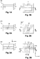
- a first embodiment of a memory cell 100 according to the invention is illustrated in the figures 1A and 1B , which represent respectively a cross-sectional view of the memory cell 100, and a top view of the oxide layer 3 of the memory cell 100.
- the cross-section is carried out along the section line II represented on the figure 1B .
- the first zone 31 extends to the periphery of the memory cell 100.
- the first formation voltage in the doped edges of the memory cell 100 is higher than the reference formation voltage in the undoped part of the oxide layer 3, that is to say the center of the memory cell 100.
- the memory cell can belong to a matrix comprising a multitude of memory cells adjacent to each other. It is known in the prior art to etch the oxide layer between the memory cells to avoid the formation of a switching zone between the upper electrode of a first memory cell and the lower electrode of a second cell. memory adjacent to the first memory cell. Thanks to the invention, it is no longer necessary to etch the oxide layer 3 to delimit the memory cells, the first zone 31 forming a zone exclusion for the formation of the filament.
- the oxide layer 3 can thus be shared by several memory cells, which facilitates their manufacture.
- FIG. 2A and 2B A second embodiment of a memory cell 200 according to the invention is illustrated in the figures 2A and 2B , which represent respectively a cross-sectional view of the memory cell 200, and a top view of the oxide layer 3 of the memory cell 200.
- the cross-section is carried out along the section line II-II represented on the figure 2B .
- the first area 31 is doped with silicon and the oxide layer 3 comprises a second area 32 also doped with silicon.
- the second area 32 is placed in the center of the memory cell 200.
- the substrate extends along an XY reference plane in which the first area 31 completely surrounds the second area 32.
- the atomic concentration of silicon in the second zone 32 is preferably greater than 3%.
- the second zone 32 has a second formation voltage lower than the reference formation voltage. Therefore, by reducing the formation voltage applied to the memory cell 200, the formation of the filament is favored in the second zone 32.
- the first zone 31, in which the first formation voltage is higher than the reference creates a confinement effect of the filament in the second zone 32 at the center of the memory cell 200.
- the second zone 32 forms a potential well for the formation of the switching zone while the first zone 31 forms a potential barrier .
- the formation voltage applied to the memory cell 200 it is also possible to reduce the size of the electronic circuit supplying the formation voltage, the size of the electronic circuit being directly linked to the value of the formation voltage at provide.
- the first zone 31 extends to the periphery of the memory cell 200. It is thus possible to dispense with a masking step during the manufacture of the memory cell 200, as described in more detail by the following.
- a third embodiment of a memory cell 300 according to the invention is illustrated in the figures 3A and 3B , which represent respectively a cross-sectional view of the memory cell 300, and a top view of the oxide layer 3 of the memory cell 300.
- the cross-section is carried out along the line III-III represented on the Figure 3B .
- the first area 31 is doped with silicon and the oxide layer 3 comprises a second area 32 also doped with silicon.
- the first zone 31 comprises a first portion 31a and a second portion 31b which extend along a first direction X, as well as a third portion 31c and a fourth portion 31d which extend along a second direction Y substantially orthogonal to the first direction X.
- the first portion 31a and the second portion 31b are arranged on either side of the second zone 32 so that they form, with the second zone 32, a first trench 37 extending along the first direction X.
- the third portion 31c and the fourth portion 31d are arranged on either side of the second zone 32 so that they form, with the second zone 32, a second trench 38 extending along the second direction Y.
- the first trench 37 and the second trench 38 intersect at the level of the second zone 32 which is arranged in the center of the memory cell 300.
- the atomic concentrations of silicon in the first trench 37 and in the second trench 38 are each between 0.1% and 2% and the total atomic concentration of silicon in the second zone 32, which is equal to the sum of the concentrations silicon atoms in the first trench 37 and in the second trench 38, is greater than 3%.
- the formation of the switching zone is favored in the second zone 32.
- the atomic concentrations of silicon in the first trench 37 and in the second trench 38 are each 1.5% order.
- the doping of the oxide layer 3 is preferably obtained by ion implantation.
- the minimum size of the implanted zones is therefore limited by the lithography processes.
- This configuration comprising two doping regions in the form of perpendicular trenches makes it possible to produce small-sized patterns at the intersection of the trenches whereas it would be difficult to produce these same patterns in an isolated manner, in a single lithography step.
- the present invention makes it possible to control the location of the switching zone as a function of the doping of the oxide layer 3.
- the switching zone is located at the center of the memory cell, which makes it possible to improve the characteristics of the cell memory such as retention over time and maximum number of cycles.
- the controlled location of the switching zone makes it possible to avoid etching the oxide layer 3 to delimit the memory cells, the filament not running the risk of forming between two adjacent cells.
- Another aspect of the invention relates to a method 500 of manufacturing a memory cell such as those described previously.
- the memory cell belongs to a matrix comprising a multitude of memory cells arranged in rows and columns. For reasons of simplification, only a few memory cells are shown in the figures accompanying the description of the steps of the manufacturing method 500.
- the manufacturing process 500 comprises a step 502 of forming the lower electrode 1, a step 504 of forming the oxide layer 3 and a step 506 of forming the upper electrode 2.
- deposition processes such as sputtering, atomic layer deposition, also called ALD for "Atomic Layer Deposition” in English, physical vapor deposition, also called PVD for "Physical Vapor Deposition” in English, or chemical vapor deposition, also called CVD for "Chemical Vapor Deposition” in English.
- an electrically conductive layer is deposited on oxide layer 3. This conductive layer is then etched to form upper electrode 2 of each memory cell. The etching of the conductive layer follows, for example, a line represented by dotted lines on the Figures 6B, 7B and 8C . The upper electrode 2 of each memory cell is thus individually insulated.
- the conductive layer can be etched so as to form rows or columns of memory cells, each row or each column having the same upper electrode 2 .
- the oxide layer 3 can therefore be common to several memory cells. Taking for example the case of the crossbar architecture in which the upper electrode 2 is common to several memory cells arranged in a column (respectively in a row), the oxide layer 3 can be etched at the same time as the conductive layer intended in forming the lower electrode 1 so as to form rows (respectively columns) of memory cells.
- the manufacturing method 500 also includes a step 510 of forming in the oxide layer 3 the first zone 31 doped with the doping element, that is to say aluminum or silicon as regards the embodiment of the Figure 1A , and silicon with respect to the embodiments of the figures 2A and 2B .
- the step of forming the first zone 31 includes a first step 511 of ion implantation of aluminum or silicon. Ion implantation is a very well controlled process, which makes it possible to precisely obtain the desired doping in the oxide layer 3.
- the first implantation step 511 is carried out in the first zone 31.
- the first implantation step 511 is advantageously carried out at a first dose chosen so as to obtain the desired atomic concentration of doping elements.
- silicon can be implanted at an energy of 4keV with a dose of between 8 ⁇ 10 13 atoms per cm -2 and 1.6 ⁇ 10 15 atoms per cm -2 .
- the first implantation step 511 advantageously includes a first operation of masking the oxide layer 3 so as to expose the first zone 31 to ion implantation. To do this, a first mask 41 is placed on the oxide layer 3.
- the first mask 41 has a pattern which differs from one embodiment to another.
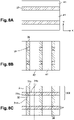
- the figures 6A and 6B show the pattern used to get memory cell 100 from the Figure 1A .
- the first silicon ion implantation step 511 is advantageously carried out over the entire surface of the oxide layer 3. It is thus possible to save the first masking operation, which represents a saving of time and money .
- the formation step 510 also comprises a second step 512 of ion implantation of the silicon in the second zone 32 of the oxide layer 3.
- the second implantation step 512 advantageously comprises a second masking operation of the oxide layer 3 so as to expose the second zone 32 to ion implantation.
- a second mask 42 is placed on the oxide layer 3.
- the second mask 42 has a pattern which differs from one embodiment to another.
- the figures 7A and 7B show the second mask 42 used to obtain the memory cell 200 from the figure 2A .
- the second implantation step 512 is carried out at a second dose chosen so that the total atomic concentration of silicon in the second zone 32 is greater than 3%. Given that the first implantation step 511 is performed over the entire surface of the oxide layer 3, the second implanted dose is added to the first dose implanted in the second zone 32.
- the figures 8A to 8C show a particularly advantageous mode of implementation of the manufacturing method 500 making it possible to obtain the memory cell 300 of the Figure 3A .
- the figure 8A shows the first mask 41 used to form, during the first implantation step 511, the first trenches 37 extending along the first direction X.
- figure 8B shows the second mask 42 used to form, during the second implantation step 512, the second trenches 38 extending along the second direction Y.
- the intersection of the trenches 31, 32 form the second zones 32 in which the implanted doses are added.
- the doses to be implanted are chosen so that the atomic concentration of silicon in each trench 37, 38 is between 0.1% and 2% and that the total atomic concentration of silicon in the second zone 32 is greater than 3% .
- the formation of the switching zone is favored in the second zone 32.
- This mode of implementation fully exploits the profile of variation of the formation voltage as a function of the atomic concentration, illustrated in figure 4 . It is thus possible to easily form, by two successive masking operations, intersection patterns of very small dimensions, for example less than 10 nm, which otherwise would be difficult to produce in a single masking operation.
- the upper electrode 2 of each cell 300 is formed so as to be placed above the second zone 32, as represented by the dotted lines on the Fig. 8C .
- the first implantation step 511 and the second implantation step 512 can be executed in any order.
- the various masking operations of the oxide layer 3 are carried out by means of known lithography processes such as lithography in the deep ultraviolet, by electron beam, or based on the self-assembly of block copolymers.
- the figure 9 illustrates the second ion implantation step according to another embodiment of the method of the invention.
- the memory cell is formed on an electrical contact 5 which electrically connects the first electrode 1 for example to a circuit (not shown) formed in lower layers on the substrate.
- This memory cell is encapsulated in an insulating material 7, such as a silicon oxide (SiO x ), which is then planarized for example by means of a chemical-mechanical planarization process, also called CMP for "chemical-mechanical planarization .
- a chemical-mechanical planarization process also called CMP for "chemical-mechanical planarization .
- An opening 71 is made in the insulating material 7 so as to be able to form an electrical contact on the second electrode 2.
- the insulating material 7 is used as a mask to carry out the second ion implantation step, symbolized by arrows 8, through opening 71.
- the switching zone of the memory cell is thus aligned with the electrical contact of the second electrode 2, which is particularly advantageous in the case of memory cells having small lateral dimensions, for example substantially equal to those of the electrical contact.
- multiple ion implantation steps can be performed using a single mask.
- the implanted ions come from a source which, at each implantation step, forms an angle of incidence with a direction normal to the plane of the substrate.
- the relative position of the source with respect to the substrate is then modified so that the implanted ions come from several directions. For example, in the case where four implantation steps are carried out, the relative position of the source with respect to the substrate can be modified by a quarter turn.
- This implementation variant makes it possible to obtain in a zone thus doped a gradient of the atomic concentration of doping elements which implies a gradient of the formation voltage.
- the implanted zone is delimited by the edges of the mask. Since the source of the ions is inclined with respect to the plane of the substrate, the atomic concentration of doping elements in the implanted zone is lowest near the edges of the mask and increases gradually to the center of the implanted zone.
- the implantation steps can be carried out, all or only in part, after the deposition on the oxide layer 3 of the electrically conductive layer intended to form the upper electrode 2.
- the doping elements are then implanted through the conductive layer.
- the masks used to deposit metallic contacts on the upper electrode 2 can be used beforehand to implant the doping elements in the oxide layer 3.
Landscapes
- Engineering & Computer Science (AREA)
- Manufacturing & Machinery (AREA)
- Semiconductor Memories (AREA)
- Non-Volatile Memory (AREA)
Claims (13)
- Resistive, nicht flüchtige Speicherzelle (100, 200, 300), umfassend eine erste Elektrode (1), eine zweite Elektrode (2) und eine Oxidschicht (3), die zwischen der ersten Elektrode und der zweiten Elektrode angeordnet ist, wobei die Speicherzelle geeignet ist, umkehrbar umzuschalten zwischen:- einem Zustand mit starkem Widerstand, der durch Anwenden einer ersten Polarisationsspannung zwischen der ersten Elektrode und der zweiten Elektrode erhalten ist; und;- einem Zustand mit geringem Widerstand durch Anwenden einer zweiten Polarisationsspannung zwischen der ersten Elektrode und der zweiten Elektrode;wobei die Oxidschicht einen Umschaltbereich umfasst, der einen privilegierten Umschaltbereich für den Strom umfasst, der die Speicherzelle durchströmt, wenn die Speicherzelle im Zustand mit niedrigem Widerstand ist, wobei die Speicherzelle dadurch gekennzeichnet ist, dass die Oxidschicht einen ersten, mit Aluminium oder Silizium gedopten Bereich (31) umfasst,wobei das Aluminium oder das Silizium in dem ersten Bereich in einer Atomkonzentration vorhanden ist, die derart ausgewählt ist, dass der Umschaltbereich außerhalb des ersten Bereichs angeordnet ist.
- Speicherzelle (100, 200, 300) gemäß Anspruch 1, dadurch gekennzeichnet, dass der erste Bereich (31) sich an der Peripherie der Speicherzelle erstreckt.
- Speicherzelle (100, 200, 300) gemäß irgendeinem der Ansprüche 1 bis 2, dadurch gekennzeichnet, dass der erste Bereich (31) mit Silizium gedopt ist, wobei die Atomkonzentration an Silizium in dem ersten Bereich zwischen 0,1 % und 2 % inbegriffen ist
- Speicherzelle (200, 300) gemäß Anspruch 3, dadurch gekennzeichnet, dass die Oxidschicht (3) einen zweiten, mit Silizium gedopten Bereich (32) umfasst, wobei das Silizium in dem zweiten Bereich in einer Atomkonzentration vorhanden ist, die derart ausgewählt ist, dass der Umschaltbereich in dem zweiten Bereich angeordnet ist.
- Speicherzelle (200) gemäß Anspruch 4, dadurch gekennzeichnet, dass der erste Bereich den zweiten Bereich vollständig umschließt.
- Speicherzelle (300) gemäß Anspruch 4, dadurch gekennzeichnet, dass der erste Bereich (31) umfasst:- einen ersten Abschnitt und einen zweiten Abschnitt, die sich auf jeder Seite des zweiten Bereichs gemäß einer ersten Richtung (X) erstrecken;- einen dritten Abschnitt und einen vierten Abschnitt, die sich auf jeder Seite des zweiten Bereichs gemäß einer zweiten Richtung (Y) erstrecken, die zur ersten Richtung deutlich orthogonal ist.
- Speicherzelle (200, 300) gemäß irgendeinem der Ansprüche 1 bis 6, dadurch gekennzeichnet, dass die Atomkonzentration (C) aus Silizium in dem zweiten Bereich höher als 3 % ist.
- Speicherzelle (100, 200, 300) gemäß irgendeinem der Ansprüche 1 bis 7, dadurch gekennzeichnet, dass die Oxidschicht (3) ein Material aus den folgenden umfasst: Hafniumoxid, Tantaloxid.
- Herstellungsverfahren (500) einer resistiven, nicht flüchtigen Speicherzelle (100, 200, 300), umfassend eine erste Elektrode (1), eine zweite Elektrode (2) und eine Oxidschicht (3), die zwischen der ersten Elektrode und der zweiten Elektrode angeordnet ist, wobei die Speicherzelle geeignet ist, umkehrbar umzuschalten zwischen:- einem starken Widerstandszustand, der durch Anwenden einer ersten Polarisationsspannung zwischen der ersten Elektrode und der zweiten Elektrode erhalten wird; und- einem schwachen Widerstandszustand durch Anwenden einer zweiten Polarisationsspannung zwischen der ersten Elektrode und der zweiten Elektrode;wobei die Oxidschicht einen Umschaltbereich umfasst, der einen privilegierten Leitungsweg für den Strom bildet, der die Speicherzelle durchströmt, wenn die Speicherzelle im schwachen Widerstandszustand ist, wobei das Verfahren dadurch gekennzeichnet ist, dass es einen Bildungsschritt (510) in der Oxidschicht eines ersten mit Aluminium oder Silizium gedopten Bereichs (31) umfasst, wobei das Aluminium oder das Silizium in dem ersten Bereich in einer Atomkonzentration vorhanden ist, die derart ausgewählt wird, dass der Umschaltbereich außerhalb des ersten Bereichs angeordnet ist.
- Verfahren (500) gemäß Anspruch 9, dadurch gekennzeichnet, dass der Bildungsschritt einen ersten ionischen Aluminium- oder Silizium-Einbauschritt in dem ersten Bereich umfasst.
- Verfahren (500) gemäß Anspruch 9, dadurch gekennzeichnet, dass der Bildungsschritt einen ersten ionischen Silizium-Einbauschritt in einer ersten Region der Oxidschicht und einen zweiten ionischen Silizium-Einbauschritt in einer zweiten Region der Oxidschicht umfasst, wobei die erste Region und die zweite Region wenigstens teilweise zusammenfallen und bilden:- den ersten Bereich der Oxidschicht, in der die erste Region und die zweite Region nicht zusammenfallen; und- einen zweiten Bereich der Oxidschicht, in der die erste Region und die zweite Region zusammenfallen;wobei der erste Einbauschritt (510) und der zweite Einbauschritt in derartigen Dosen durchgeführt werden, dass das Silizium in dem zweiten Bereich in einer Gesamt-Atomkonzentration vorhanden ist, die derart ausgewählt wird, dass der Umschaltbereich in dem zweiten Bereich angeordnet ist.
- Verfahren (500) gemäß Anspruch 11, dadurch gekennzeichnet, dass der erste Einbauschritt (510) eine erste Abdeckoperation der Oxidschicht (3) umfasst, die derart realisiert wird, dass die erste Region (31) eine erste Vertiefung bildet, die sich gemäß einer ersten Richtung (X) erstreckt, und dass der zweite Einbauschritt (512) eine zweite Abdeckoperation der Oxidschicht umfasst, die derart realisiert wird, dass die zweite Region (32) eine zweite Vertiefung bildet, die sich gemäß einer zweiten, zur ersten Richtung deutlich orthogonalen Richtung (Y) erstreckt, wobei die zweite Vertiefung die erste Vertiefung kreuzt, wobei der zweite Bereich per Schneiden der ersten Vertiefung und der zweiten Vertiefung gebildet wird.
- Verfahren (500) gemäß irgendeinem der Ansprüche 10 bis 12, dadurch gekennzeichnet, dass es einen Aufbringungsschritt einer zum Bilden einer Elektrode (2) bestimmten elektrisch leitenden Schicht auf der Oxidschicht (3) umfasst, wobei der erste Einbauschritt (510) und/oder der zweite Einbauschritt (512) nach dem Aufbringungsschritt der elektrisch leitenden Schicht durchgeführt werden.
Applications Claiming Priority (2)
| Application Number | Priority Date | Filing Date | Title |
|---|---|---|---|
| FR1658446A FR3056017B1 (fr) | 2016-09-09 | 2016-09-09 | Cellule memoire non-volatile resistive a base d'oxyde et son procede de fabrication |
| PCT/EP2017/072622 WO2018046683A1 (fr) | 2016-09-09 | 2017-09-08 | Cellule memoire non-volatile resistive a base d'oxyde et son procede de fabrication |
Publications (2)
| Publication Number | Publication Date |
|---|---|
| EP3510644A1 EP3510644A1 (de) | 2019-07-17 |
| EP3510644B1 true EP3510644B1 (de) | 2022-04-06 |
Family
ID=57348928
Family Applications (1)
| Application Number | Title | Priority Date | Filing Date |
|---|---|---|---|
| EP17768728.2A Active EP3510644B1 (de) | 2016-09-09 | 2017-09-08 | Oxidbasierte resistive nichtflüchtige speicherzelle und verfahren zur herstellung davon |
Country Status (4)
| Country | Link |
|---|---|
| US (1) | US11189792B2 (de) |
| EP (1) | EP3510644B1 (de) |
| FR (1) | FR3056017B1 (de) |
| WO (1) | WO2018046683A1 (de) |
Families Citing this family (4)
| Publication number | Priority date | Publication date | Assignee | Title |
|---|---|---|---|---|
| TWI708410B (zh) * | 2019-07-08 | 2020-10-21 | 華邦電子股份有限公司 | 可變電阻式記憶體及其製造方法 |
| CN112259681B (zh) * | 2019-07-22 | 2024-03-05 | 华邦电子股份有限公司 | 电阻式随机存取存储器结构及其制造方法 |
| US11456416B2 (en) * | 2020-11-19 | 2022-09-27 | International Business Machines Corporation | Resistive switching memory cell |
| KR20230060859A (ko) * | 2021-10-28 | 2023-05-08 | 에스케이하이닉스 주식회사 | 전자 장치 및 그 제조방법 |
Family Cites Families (9)
| Publication number | Priority date | Publication date | Assignee | Title |
|---|---|---|---|---|
| US8062918B2 (en) * | 2008-05-01 | 2011-11-22 | Intermolecular, Inc. | Surface treatment to improve resistive-switching characteristics |
| US8420478B2 (en) * | 2009-03-31 | 2013-04-16 | Intermolecular, Inc. | Controlled localized defect paths for resistive memories |
| US8313996B2 (en) * | 2010-09-22 | 2012-11-20 | Micron Technology, Inc. | Reactive metal implated oxide based memory |
| US20120295398A1 (en) * | 2011-05-16 | 2012-11-22 | Varian Semiconductor Equipment Associates, Inc. | Ion implant modification of resistive random access memory devices |
| US8835272B1 (en) * | 2013-02-28 | 2014-09-16 | Sandia Corporation | Passive electrically switchable circuit element having improved tunability and method for its manufacture |
| JP2014216647A (ja) * | 2013-04-29 | 2014-11-17 | エーエスエムアイピー ホールディング ビー.ブイ. | 金属ドープされた抵抗切り替え層を有する抵抗変化型メモリを製造する方法 |
| US9727258B1 (en) * | 2014-10-03 | 2017-08-08 | Crossbar, Inc. | Two-terminal memory compatibility with NAND flash memory set features type mechanisms |
| US10529921B2 (en) * | 2015-06-05 | 2020-01-07 | Australian Advanced Materials Pty Ltd | Memory structure for use in resistive random access memory devices and method for use in manufacturing a data storage device |
| US9972779B2 (en) * | 2015-12-14 | 2018-05-15 | Winbond Electronics Corp. | Resistive random access memory |
-
2016
- 2016-09-09 FR FR1658446A patent/FR3056017B1/fr not_active Expired - Fee Related
-
2017
- 2017-09-08 US US16/331,714 patent/US11189792B2/en active Active
- 2017-09-08 EP EP17768728.2A patent/EP3510644B1/de active Active
- 2017-09-08 WO PCT/EP2017/072622 patent/WO2018046683A1/fr not_active Ceased
Also Published As
| Publication number | Publication date |
|---|---|
| US11189792B2 (en) | 2021-11-30 |
| US20190280203A1 (en) | 2019-09-12 |
| FR3056017A1 (fr) | 2018-03-16 |
| FR3056017B1 (fr) | 2018-11-09 |
| WO2018046683A1 (fr) | 2018-03-15 |
| EP3510644A1 (de) | 2019-07-17 |
Similar Documents
| Publication | Publication Date | Title |
|---|---|---|
| EP3012880B1 (de) | Nicht-flüchtige hybrid-speichervorrichtung, und herstellungsverfahren einer solchen vorrichtung | |
| EP3542406B1 (de) | Verfahren zur herstellung eines resistiven speichers | |
| EP3510644B1 (de) | Oxidbasierte resistive nichtflüchtige speicherzelle und verfahren zur herstellung davon | |
| TW201030946A (en) | Nonvolatile memory cell including carbon storage element formed on a silicide layer | |
| CN113346011B (zh) | 存储器装置、集成芯片及其形成方法 | |
| EP3151296B1 (de) | Verfahren zur herstellung einer resistiven speicherzelle | |
| EP3671844B1 (de) | Herstellungsverfahren eines ferroelektrischen speichers und verfahren zur gleichzeitigen herstellung eines ferroelektrischen und eines resistiven speichers und daraus entstehende vorrichtung | |
| EP4175448B1 (de) | Verfahren zur co-herstellung eines ferroelektrischen speichers und eines resistiven oxram-speichers und vorrichtung mit einem ferroelektrischen speicher und einem resistiven oxram-speicher | |
| EP3506377B1 (de) | Elementarzelle, umfassend einen widerstandsspeicher und ein auswahlelement, ebene und matrix von ebenen umfassend eine vielzahl solcher zellen sowie zugeordnetes herstellungsverfahren | |
| TW201133636A (en) | Method of making damascene diodes using selective etching methods | |
| EP3840049A1 (de) | Elementarzelle, die einen resistiven speicher umfasst, und entsprechendes initialisierungsverfahren | |
| KR102329578B1 (ko) | 라인형 메모리 및 그 형성 방법 | |
| EP3965177A1 (de) | Resistiver speicher mit einer schaltzone zwischen zwei dielektrischen bereichen mit unterschiedlichen dotierungen und/oder dielektrizitätskonstanten | |
| EP4454444B1 (de) | Anordnung mit mindestens zwei nichtflüchtigen resistiven speichern und einem selektor, matrix und zugehöriges herstellungsverfahren | |
| EP4454443B1 (de) | Anordnung mit mindestens zwei nichtflüchtigen resistiven speichern und zwei selektoren, matrix und zugehöriges herstellungsverfahren | |
| EP3510598B1 (de) | Vorrichtung zur auswahl einer speicherzelle | |
| EP4142451B1 (de) | Verfahren zur herstellung von resistiven speicherzellen | |
| JP5840505B2 (ja) | 半導体装置の製造方法 | |
| EP4454442A1 (de) | Anordnung mit mindestens zwei wählern und zwei nichtflüchtigen resistiven speichern, zugehörige matrix und herstellungsverfahren | |
| EP4572595A1 (de) | Integrierte schaltung mit nichtflüchtigem speicher und herstellungsverfahren dafür | |
| FR3157785A1 (fr) | Dispositif de stockage ferroelectrique et procede de fabrication d’un tel dispositif | |
| FR2979467A1 (fr) | Dispositif microelectronique dote de cellules memoires resistives empilees |
Legal Events
| Date | Code | Title | Description |
|---|---|---|---|
| STAA | Information on the status of an ep patent application or granted ep patent |
Free format text: STATUS: UNKNOWN |
|
| STAA | Information on the status of an ep patent application or granted ep patent |
Free format text: STATUS: THE INTERNATIONAL PUBLICATION HAS BEEN MADE |
|
| PUAI | Public reference made under article 153(3) epc to a published international application that has entered the european phase |
Free format text: ORIGINAL CODE: 0009012 |
|
| STAA | Information on the status of an ep patent application or granted ep patent |
Free format text: STATUS: REQUEST FOR EXAMINATION WAS MADE |
|
| 17P | Request for examination filed |
Effective date: 20190321 |
|
| AK | Designated contracting states |
Kind code of ref document: A1 Designated state(s): AL AT BE BG CH CY CZ DE DK EE ES FI FR GB GR HR HU IE IS IT LI LT LU LV MC MK MT NL NO PL PT RO RS SE SI SK SM TR |
|
| AX | Request for extension of the european patent |
Extension state: BA ME |
|
| DAV | Request for validation of the european patent (deleted) | ||
| DAX | Request for extension of the european patent (deleted) | ||
| GRAP | Despatch of communication of intention to grant a patent |
Free format text: ORIGINAL CODE: EPIDOSNIGR1 |
|
| STAA | Information on the status of an ep patent application or granted ep patent |
Free format text: STATUS: GRANT OF PATENT IS INTENDED |
|
| INTG | Intention to grant announced |
Effective date: 20211028 |
|
| GRAS | Grant fee paid |
Free format text: ORIGINAL CODE: EPIDOSNIGR3 |
|
| GRAA | (expected) grant |
Free format text: ORIGINAL CODE: 0009210 |
|
| STAA | Information on the status of an ep patent application or granted ep patent |
Free format text: STATUS: THE PATENT HAS BEEN GRANTED |
|
| AK | Designated contracting states |
Kind code of ref document: B1 Designated state(s): AL AT BE BG CH CY CZ DE DK EE ES FI FR GB GR HR HU IE IS IT LI LT LU LV MC MK MT NL NO PL PT RO RS SE SI SK SM TR |
|
| REG | Reference to a national code |
Ref country code: GB Ref legal event code: FG4D Free format text: NOT ENGLISH |
|
| REG | Reference to a national code |
Ref country code: CH Ref legal event code: EP |
|
| REG | Reference to a national code |
Ref country code: AT Ref legal event code: REF Ref document number: 1482228 Country of ref document: AT Kind code of ref document: T Effective date: 20220415 |
|
| REG | Reference to a national code |
Ref country code: DE Ref legal event code: R096 Ref document number: 602017055610 Country of ref document: DE |
|
| REG | Reference to a national code |
Ref country code: IE Ref legal event code: FG4D Free format text: LANGUAGE OF EP DOCUMENT: FRENCH |
|
| REG | Reference to a national code |
Ref country code: LT Ref legal event code: MG9D |
|
| REG | Reference to a national code |
Ref country code: NL Ref legal event code: MP Effective date: 20220406 |
|
| REG | Reference to a national code |
Ref country code: AT Ref legal event code: MK05 Ref document number: 1482228 Country of ref document: AT Kind code of ref document: T Effective date: 20220406 |
|
| PG25 | Lapsed in a contracting state [announced via postgrant information from national office to epo] |
Ref country code: NL Free format text: LAPSE BECAUSE OF FAILURE TO SUBMIT A TRANSLATION OF THE DESCRIPTION OR TO PAY THE FEE WITHIN THE PRESCRIBED TIME-LIMIT Effective date: 20220406 |
|
| PG25 | Lapsed in a contracting state [announced via postgrant information from national office to epo] |
Ref country code: SE Free format text: LAPSE BECAUSE OF FAILURE TO SUBMIT A TRANSLATION OF THE DESCRIPTION OR TO PAY THE FEE WITHIN THE PRESCRIBED TIME-LIMIT Effective date: 20220406 Ref country code: PT Free format text: LAPSE BECAUSE OF FAILURE TO SUBMIT A TRANSLATION OF THE DESCRIPTION OR TO PAY THE FEE WITHIN THE PRESCRIBED TIME-LIMIT Effective date: 20220808 Ref country code: NO Free format text: LAPSE BECAUSE OF FAILURE TO SUBMIT A TRANSLATION OF THE DESCRIPTION OR TO PAY THE FEE WITHIN THE PRESCRIBED TIME-LIMIT Effective date: 20220706 Ref country code: LT Free format text: LAPSE BECAUSE OF FAILURE TO SUBMIT A TRANSLATION OF THE DESCRIPTION OR TO PAY THE FEE WITHIN THE PRESCRIBED TIME-LIMIT Effective date: 20220406 Ref country code: HR Free format text: LAPSE BECAUSE OF FAILURE TO SUBMIT A TRANSLATION OF THE DESCRIPTION OR TO PAY THE FEE WITHIN THE PRESCRIBED TIME-LIMIT Effective date: 20220406 Ref country code: GR Free format text: LAPSE BECAUSE OF FAILURE TO SUBMIT A TRANSLATION OF THE DESCRIPTION OR TO PAY THE FEE WITHIN THE PRESCRIBED TIME-LIMIT Effective date: 20220707 Ref country code: FI Free format text: LAPSE BECAUSE OF FAILURE TO SUBMIT A TRANSLATION OF THE DESCRIPTION OR TO PAY THE FEE WITHIN THE PRESCRIBED TIME-LIMIT Effective date: 20220406 Ref country code: ES Free format text: LAPSE BECAUSE OF FAILURE TO SUBMIT A TRANSLATION OF THE DESCRIPTION OR TO PAY THE FEE WITHIN THE PRESCRIBED TIME-LIMIT Effective date: 20220406 Ref country code: BG Free format text: LAPSE BECAUSE OF FAILURE TO SUBMIT A TRANSLATION OF THE DESCRIPTION OR TO PAY THE FEE WITHIN THE PRESCRIBED TIME-LIMIT Effective date: 20220706 Ref country code: AT Free format text: LAPSE BECAUSE OF FAILURE TO SUBMIT A TRANSLATION OF THE DESCRIPTION OR TO PAY THE FEE WITHIN THE PRESCRIBED TIME-LIMIT Effective date: 20220406 |
|
| REG | Reference to a national code |
Ref country code: DE Ref legal event code: R079 Ref document number: 602017055610 Country of ref document: DE Free format text: PREVIOUS MAIN CLASS: H01L0045000000 Ipc: H10N0070000000 |
|
| PG25 | Lapsed in a contracting state [announced via postgrant information from national office to epo] |
Ref country code: RS Free format text: LAPSE BECAUSE OF FAILURE TO SUBMIT A TRANSLATION OF THE DESCRIPTION OR TO PAY THE FEE WITHIN THE PRESCRIBED TIME-LIMIT Effective date: 20220406 Ref country code: PL Free format text: LAPSE BECAUSE OF FAILURE TO SUBMIT A TRANSLATION OF THE DESCRIPTION OR TO PAY THE FEE WITHIN THE PRESCRIBED TIME-LIMIT Effective date: 20220406 Ref country code: LV Free format text: LAPSE BECAUSE OF FAILURE TO SUBMIT A TRANSLATION OF THE DESCRIPTION OR TO PAY THE FEE WITHIN THE PRESCRIBED TIME-LIMIT Effective date: 20220406 Ref country code: IS Free format text: LAPSE BECAUSE OF FAILURE TO SUBMIT A TRANSLATION OF THE DESCRIPTION OR TO PAY THE FEE WITHIN THE PRESCRIBED TIME-LIMIT Effective date: 20220806 |
|
| REG | Reference to a national code |
Ref country code: DE Ref legal event code: R097 Ref document number: 602017055610 Country of ref document: DE |
|
| PG25 | Lapsed in a contracting state [announced via postgrant information from national office to epo] |
Ref country code: SM Free format text: LAPSE BECAUSE OF FAILURE TO SUBMIT A TRANSLATION OF THE DESCRIPTION OR TO PAY THE FEE WITHIN THE PRESCRIBED TIME-LIMIT Effective date: 20220406 Ref country code: SK Free format text: LAPSE BECAUSE OF FAILURE TO SUBMIT A TRANSLATION OF THE DESCRIPTION OR TO PAY THE FEE WITHIN THE PRESCRIBED TIME-LIMIT Effective date: 20220406 Ref country code: RO Free format text: LAPSE BECAUSE OF FAILURE TO SUBMIT A TRANSLATION OF THE DESCRIPTION OR TO PAY THE FEE WITHIN THE PRESCRIBED TIME-LIMIT Effective date: 20220406 Ref country code: EE Free format text: LAPSE BECAUSE OF FAILURE TO SUBMIT A TRANSLATION OF THE DESCRIPTION OR TO PAY THE FEE WITHIN THE PRESCRIBED TIME-LIMIT Effective date: 20220406 Ref country code: DK Free format text: LAPSE BECAUSE OF FAILURE TO SUBMIT A TRANSLATION OF THE DESCRIPTION OR TO PAY THE FEE WITHIN THE PRESCRIBED TIME-LIMIT Effective date: 20220406 Ref country code: CZ Free format text: LAPSE BECAUSE OF FAILURE TO SUBMIT A TRANSLATION OF THE DESCRIPTION OR TO PAY THE FEE WITHIN THE PRESCRIBED TIME-LIMIT Effective date: 20220406 |
|
| PLBE | No opposition filed within time limit |
Free format text: ORIGINAL CODE: 0009261 |
|
| STAA | Information on the status of an ep patent application or granted ep patent |
Free format text: STATUS: NO OPPOSITION FILED WITHIN TIME LIMIT |
|
| 26N | No opposition filed |
Effective date: 20230110 |
|
| PG25 | Lapsed in a contracting state [announced via postgrant information from national office to epo] |
Ref country code: AL Free format text: LAPSE BECAUSE OF FAILURE TO SUBMIT A TRANSLATION OF THE DESCRIPTION OR TO PAY THE FEE WITHIN THE PRESCRIBED TIME-LIMIT Effective date: 20220406 |
|
| PG25 | Lapsed in a contracting state [announced via postgrant information from national office to epo] |
Ref country code: MC Free format text: LAPSE BECAUSE OF FAILURE TO SUBMIT A TRANSLATION OF THE DESCRIPTION OR TO PAY THE FEE WITHIN THE PRESCRIBED TIME-LIMIT Effective date: 20220406 |
|
| REG | Reference to a national code |
Ref country code: CH Ref legal event code: PL |
|
| REG | Reference to a national code |
Ref country code: BE Ref legal event code: MM Effective date: 20220930 |
|
| PG25 | Lapsed in a contracting state [announced via postgrant information from national office to epo] |
Ref country code: SI Free format text: LAPSE BECAUSE OF FAILURE TO SUBMIT A TRANSLATION OF THE DESCRIPTION OR TO PAY THE FEE WITHIN THE PRESCRIBED TIME-LIMIT Effective date: 20220406 |
|
| PG25 | Lapsed in a contracting state [announced via postgrant information from national office to epo] |
Ref country code: LU Free format text: LAPSE BECAUSE OF NON-PAYMENT OF DUE FEES Effective date: 20220908 |
|
| PG25 | Lapsed in a contracting state [announced via postgrant information from national office to epo] |
Ref country code: LI Free format text: LAPSE BECAUSE OF NON-PAYMENT OF DUE FEES Effective date: 20220930 Ref country code: IE Free format text: LAPSE BECAUSE OF NON-PAYMENT OF DUE FEES Effective date: 20220908 Ref country code: CH Free format text: LAPSE BECAUSE OF NON-PAYMENT OF DUE FEES Effective date: 20220930 |
|
| PG25 | Lapsed in a contracting state [announced via postgrant information from national office to epo] |
Ref country code: BE Free format text: LAPSE BECAUSE OF NON-PAYMENT OF DUE FEES Effective date: 20220930 |
|
| PG25 | Lapsed in a contracting state [announced via postgrant information from national office to epo] |
Ref country code: IT Free format text: LAPSE BECAUSE OF FAILURE TO SUBMIT A TRANSLATION OF THE DESCRIPTION OR TO PAY THE FEE WITHIN THE PRESCRIBED TIME-LIMIT Effective date: 20220406 |
|
| PG25 | Lapsed in a contracting state [announced via postgrant information from national office to epo] |
Ref country code: HU Free format text: LAPSE BECAUSE OF FAILURE TO SUBMIT A TRANSLATION OF THE DESCRIPTION OR TO PAY THE FEE WITHIN THE PRESCRIBED TIME-LIMIT; INVALID AB INITIO Effective date: 20170908 |
|
| PG25 | Lapsed in a contracting state [announced via postgrant information from national office to epo] |
Ref country code: CY Free format text: LAPSE BECAUSE OF FAILURE TO SUBMIT A TRANSLATION OF THE DESCRIPTION OR TO PAY THE FEE WITHIN THE PRESCRIBED TIME-LIMIT Effective date: 20220406 |
|
| PG25 | Lapsed in a contracting state [announced via postgrant information from national office to epo] |
Ref country code: MK Free format text: LAPSE BECAUSE OF FAILURE TO SUBMIT A TRANSLATION OF THE DESCRIPTION OR TO PAY THE FEE WITHIN THE PRESCRIBED TIME-LIMIT Effective date: 20220406 |
|
| PG25 | Lapsed in a contracting state [announced via postgrant information from national office to epo] |
Ref country code: TR Free format text: LAPSE BECAUSE OF FAILURE TO SUBMIT A TRANSLATION OF THE DESCRIPTION OR TO PAY THE FEE WITHIN THE PRESCRIBED TIME-LIMIT Effective date: 20220406 |
|
| PG25 | Lapsed in a contracting state [announced via postgrant information from national office to epo] |
Ref country code: MT Free format text: LAPSE BECAUSE OF FAILURE TO SUBMIT A TRANSLATION OF THE DESCRIPTION OR TO PAY THE FEE WITHIN THE PRESCRIBED TIME-LIMIT Effective date: 20220406 |
|
| PG25 | Lapsed in a contracting state [announced via postgrant information from national office to epo] |
Ref country code: BG Free format text: LAPSE BECAUSE OF FAILURE TO SUBMIT A TRANSLATION OF THE DESCRIPTION OR TO PAY THE FEE WITHIN THE PRESCRIBED TIME-LIMIT Effective date: 20220406 |
|
| PG25 | Lapsed in a contracting state [announced via postgrant information from national office to epo] |
Ref country code: BG Free format text: LAPSE BECAUSE OF FAILURE TO SUBMIT A TRANSLATION OF THE DESCRIPTION OR TO PAY THE FEE WITHIN THE PRESCRIBED TIME-LIMIT Effective date: 20220406 |
|
| PGFP | Annual fee paid to national office [announced via postgrant information from national office to epo] |
Ref country code: DE Payment date: 20250919 Year of fee payment: 9 |
|
| PGFP | Annual fee paid to national office [announced via postgrant information from national office to epo] |
Ref country code: GB Payment date: 20250923 Year of fee payment: 9 |
|
| PGFP | Annual fee paid to national office [announced via postgrant information from national office to epo] |
Ref country code: FR Payment date: 20250924 Year of fee payment: 9 |