EP3965276A1 - Circuit de filtre à compensation d'harmonique - Google Patents
Circuit de filtre à compensation d'harmonique Download PDFInfo
- Publication number
- EP3965276A1 EP3965276A1 EP21164285.5A EP21164285A EP3965276A1 EP 3965276 A1 EP3965276 A1 EP 3965276A1 EP 21164285 A EP21164285 A EP 21164285A EP 3965276 A1 EP3965276 A1 EP 3965276A1
- Authority
- EP
- European Patent Office
- Prior art keywords
- voltage
- capacitor
- freewheeling
- coupled
- filter circuit
- Prior art date
- Legal status (The legal status is an assumption and is not a legal conclusion. Google has not performed a legal analysis and makes no representation as to the accuracy of the status listed.)
- Granted
Links
Images


Classifications
-
- H—ELECTRICITY
- H02—GENERATION; CONVERSION OR DISTRIBUTION OF ELECTRIC POWER
- H02M—APPARATUS FOR CONVERSION BETWEEN AC AND AC, BETWEEN AC AND DC, OR BETWEEN DC AND DC, AND FOR USE WITH MAINS OR SIMILAR POWER SUPPLY SYSTEMS; CONVERSION OF DC OR AC INPUT POWER INTO SURGE OUTPUT POWER; CONTROL OR REGULATION THEREOF
- H02M1/00—Details of apparatus for conversion
- H02M1/42—Circuits or arrangements for compensating for or adjusting power factor in converters or inverters
- H02M1/4208—Arrangements for improving power factor of AC input
- H02M1/4266—Arrangements for improving power factor of AC input using passive elements
-
- H—ELECTRICITY
- H02—GENERATION; CONVERSION OR DISTRIBUTION OF ELECTRIC POWER
- H02M—APPARATUS FOR CONVERSION BETWEEN AC AND AC, BETWEEN AC AND DC, OR BETWEEN DC AND DC, AND FOR USE WITH MAINS OR SIMILAR POWER SUPPLY SYSTEMS; CONVERSION OF DC OR AC INPUT POWER INTO SURGE OUTPUT POWER; CONTROL OR REGULATION THEREOF
- H02M1/00—Details of apparatus for conversion
- H02M1/12—Arrangements for reducing harmonics from AC input or output
- H02M1/126—Arrangements for reducing harmonics from AC input or output using passive filters
-
- H—ELECTRICITY
- H02—GENERATION; CONVERSION OR DISTRIBUTION OF ELECTRIC POWER
- H02M—APPARATUS FOR CONVERSION BETWEEN AC AND AC, BETWEEN AC AND DC, OR BETWEEN DC AND DC, AND FOR USE WITH MAINS OR SIMILAR POWER SUPPLY SYSTEMS; CONVERSION OF DC OR AC INPUT POWER INTO SURGE OUTPUT POWER; CONTROL OR REGULATION THEREOF
- H02M7/00—Conversion of AC power input into DC power output; Conversion of DC power input into AC power output
- H02M7/02—Conversion of AC power input into DC power output without possibility of reversal
- H02M7/04—Conversion of AC power input into DC power output without possibility of reversal by static converters
- H02M7/06—Conversion of AC power input into DC power output without possibility of reversal by static converters using discharge tubes without control electrode or semiconductor devices without control electrode
-
- H—ELECTRICITY
- H02—GENERATION; CONVERSION OR DISTRIBUTION OF ELECTRIC POWER
- H02J—ELECTRIC POWER NETWORKS; CIRCUIT ARRANGEMENTS OR SYSTEMS FOR SUPPLYING OR DISTRIBUTING ELECTRIC POWER; SYSTEMS FOR STORING ELECTRIC ENERGY
- H02J50/00—Circuit arrangements or systems for wireless supply or distribution of electric power
- H02J50/001—Energy harvesting or scavenging
-
- H—ELECTRICITY
- H02—GENERATION; CONVERSION OR DISTRIBUTION OF ELECTRIC POWER
- H02J—ELECTRIC POWER NETWORKS; CIRCUIT ARRANGEMENTS OR SYSTEMS FOR SUPPLYING OR DISTRIBUTING ELECTRIC POWER; SYSTEMS FOR STORING ELECTRIC ENERGY
- H02J50/00—Circuit arrangements or systems for wireless supply or distribution of electric power
- H02J50/10—Circuit arrangements or systems for wireless supply or distribution of electric power using inductive coupling
-
- H—ELECTRICITY
- H02—GENERATION; CONVERSION OR DISTRIBUTION OF ELECTRIC POWER
- H02M—APPARATUS FOR CONVERSION BETWEEN AC AND AC, BETWEEN AC AND DC, OR BETWEEN DC AND DC, AND FOR USE WITH MAINS OR SIMILAR POWER SUPPLY SYSTEMS; CONVERSION OF DC OR AC INPUT POWER INTO SURGE OUTPUT POWER; CONTROL OR REGULATION THEREOF
- H02M1/00—Details of apparatus for conversion
- H02M1/0003—Details of control, feedback or regulation circuits
- H02M1/0006—Arrangements for supplying an adequate voltage to the control circuit of converters
-
- H—ELECTRICITY
- H02—GENERATION; CONVERSION OR DISTRIBUTION OF ELECTRIC POWER
- H02M—APPARATUS FOR CONVERSION BETWEEN AC AND AC, BETWEEN AC AND DC, OR BETWEEN DC AND DC, AND FOR USE WITH MAINS OR SIMILAR POWER SUPPLY SYSTEMS; CONVERSION OF DC OR AC INPUT POWER INTO SURGE OUTPUT POWER; CONTROL OR REGULATION THEREOF
- H02M1/00—Details of apparatus for conversion
- H02M1/14—Arrangements for reducing ripples from DC input or output
- H02M1/143—Arrangements for reducing ripples from DC input or output using compensating arrangements
-
- H—ELECTRICITY
- H02—GENERATION; CONVERSION OR DISTRIBUTION OF ELECTRIC POWER
- H02M—APPARATUS FOR CONVERSION BETWEEN AC AND AC, BETWEEN AC AND DC, OR BETWEEN DC AND DC, AND FOR USE WITH MAINS OR SIMILAR POWER SUPPLY SYSTEMS; CONVERSION OF DC OR AC INPUT POWER INTO SURGE OUTPUT POWER; CONTROL OR REGULATION THEREOF
- H02M1/00—Details of apparatus for conversion
- H02M1/42—Circuits or arrangements for compensating for or adjusting power factor in converters or inverters
- H02M1/4208—Arrangements for improving power factor of AC input
- H02M1/4216—Arrangements for improving power factor of AC input operating from a three-phase input voltage
-
- H—ELECTRICITY
- H02—GENERATION; CONVERSION OR DISTRIBUTION OF ELECTRIC POWER
- H02M—APPARATUS FOR CONVERSION BETWEEN AC AND AC, BETWEEN AC AND DC, OR BETWEEN DC AND DC, AND FOR USE WITH MAINS OR SIMILAR POWER SUPPLY SYSTEMS; CONVERSION OF DC OR AC INPUT POWER INTO SURGE OUTPUT POWER; CONTROL OR REGULATION THEREOF
- H02M1/00—Details of apparatus for conversion
- H02M1/42—Circuits or arrangements for compensating for or adjusting power factor in converters or inverters
- H02M1/4208—Arrangements for improving power factor of AC input
- H02M1/4275—Arrangements for improving power factor of AC input by adding an auxiliary output voltage in series to the input
-
- Y—GENERAL TAGGING OF NEW TECHNOLOGICAL DEVELOPMENTS; GENERAL TAGGING OF CROSS-SECTIONAL TECHNOLOGIES SPANNING OVER SEVERAL SECTIONS OF THE IPC; TECHNICAL SUBJECTS COVERED BY FORMER USPC CROSS-REFERENCE ART COLLECTIONS [XRACs] AND DIGESTS
- Y02—TECHNOLOGIES OR APPLICATIONS FOR MITIGATION OR ADAPTATION AGAINST CLIMATE CHANGE
- Y02B—CLIMATE CHANGE MITIGATION TECHNOLOGIES RELATED TO BUILDINGS, e.g. HOUSING, HOUSE APPLIANCES OR RELATED END-USER APPLICATIONS
- Y02B70/00—Technologies for an efficient end-user side electric power management and consumption
- Y02B70/10—Technologies improving the efficiency by using switched-mode power supplies [SMPS], i.e. efficient power electronics conversion e.g. power factor correction or reduction of losses in power supplies or efficient standby modes
Definitions
- the present disclosure relates to a filter circuit with harmonic compensation, and more particularly to a filter circuit with harmonic compensation by using passive electronic components to simplify circuit control and reduce circuit cost.
- a total harmonic distortion is an indicator of a harmonic distortion degree of an electrical signal, and it is defined as the ratio of the sum of the powers of all harmonic components to the power of the fundamental frequency. Distortion factor, a closely related term, is sometimes used as a synonym. The greater the total harmonic distortion, the greater the proportion of harmonic components. Harmonic distortion means that some unwanted signals are superimposed on the input signal due to non-linear factors, and these unwanted signals are all multiples of the original input signal.
- the filter circuit with harmonic compensation is coupled to a bridge rectifying circuit receiving an AC voltage and an input capacitor.
- the bridge rectifying circuit includes a live wire end, a neutral wire end, a positive end, and a negative end.
- the filter circuit includes a freewheeling capacitor, a freewheeling switch, and a unidirectional switch. A first end of the freewheeling capacitor is coupled to the live wire end. A first end of the freewheeling switch is coupled to a second end of the freewheeling capacitor, and a second end of the freewheeling switch is coupled to the positive end and the input capacitor.
- a first end of the unidirectional switch is coupled to the freewheeling capacitor and the freewheeling switch, and a second end of the unidirectional switch receives a voltage source.
- a first conduction voltage of the freewheeling switch is greater than a second conduction voltage between the live wire end and the positive end of the bridge rectifying circuit.
- the main purpose and effect of the present disclosure are to use a circuit structure in which a first diode in series with a second diode as a clamping circuit so that a voltage across the two diodes is greater than a voltage across the bridge rectifying diode. Therefore, the freewheeling capacitor will not generate a negative voltage when the bridge rectifying diode and the freewheeling switch are both forward biased, thereby increasing the harmonic compensation effect of the filter circuit.
- FIG. 1 shows a circuit diagram of a filter circuit with harmonic compensation according to the present disclosure.
- the filter circuit 100 with harmonic compensation (hereinafter “filter circuit”) provides a harmonic compensation of an input current Iin to reduce the harmonic distortion of the input current Iin waveform.
- a bridge rectifying circuit 200 includes four bridge rectifying diodes Db1-Db4, which receive an AC voltage Vac through a live wire end L and a neutral wire end N, and provide a half-wave voltage Vh from a positive end A and a negative end B. The half-wave voltage Vh is filtered by an input capacitor Cin to provide a DC voltage Vdc to an electronic apparatus 300.
- the detailed description of the four bridge rectifying diodes Db1-Db4 will be made as follows.
- the filter circuit 100 is coupled to the bridge rectifying circuit 200 and the input capacitor Cin, and the filter circuit 100 includes a freewheeling capacitor Cf, a freewheeling switch 10, and a unidirectional switch D.
- a first end of the freewheeling capacitor Cf is coupled to the live wire end L
- a second end of the freewheeling capacitor Cf is coupled to a first end of the freewheeling switch 10 and a first end of the unidirectional switch D
- a second end of the freewheeling switch 10 is coupled to the positive end A and a first end of the input capacitor Cin.
- a second end of the unidirectional switch D is coupled to a voltage source Vs, and the voltage source Vs charges the freewheeling capacitor Cf through the unidirectional switch D.
- the unidirectional switch D is, for example but not limited to, a diode. Any circuit element that enables the voltage source Vs to charge the freewheeling capacitor Cf and blocks the energy back to the voltage source Vs when the freewheeling capacitor Cf is discharged should be embraced within the scope of the present disclosure.
- a switch with corresponding control circuit is used.
- the filter circuit 100 further includes a power generation circuit 20, and the power generation circuit 20 may provide the voltage source Vs.
- a first end of the power generation circuit 20 is coupled to the second end of the unidirectional switch D, and a second end of the power generation circuit 20 is coupled to the negative end B, i.e., a ground end GND
- the freewheeling switch 10 mainly provides a discharge path from the freewheeling capacitor Cf to the input capacitor Cin.
- the freewheeling switch 10 includes a first diode D1 and a second diode D2 connected to the first diode D1 in series.
- An anode of the first diode D1 is coupled to the second end of the freewheeling capacitor Cf and the first end of the unidirectional switch D, and a cathode of the second diode D2 is coupled to the positive end A and the input capacitor Cin.
- the power generation circuit 20 includes an auxiliary winding 22 and a voltage stabilizing capacitor Cs. A first end of the auxiliary winding 22 is coupled to the negative end B.
- a first end of the voltage stabilizing capacitor Cs is coupled to a second end of the auxiliary winding 22, and a second end of the voltage stabilizing capacitor Cs is coupled to the negative end B.
- the auxiliary winding 22 generates an auxiliary voltage Vaux to charge the voltage stabilizing capacitor Cs so that the voltage source Vs is established on the voltage stabilizing capacitor Cs.
- the auxiliary winding 22 is mainly coupled to the electronic apparatus 300, such as a power converter having transformer (not shown), and an auxiliary voltage Vaux is induced by the coupling of the transformer.
- the voltage stabilizing capacitor Cs is connected in parallel with the auxiliary winding 22, so that the auxiliary voltage Vaux becomes a stable voltage source Vs and is provided to the controller IC, thereby achieving stable operation of the electronic apparatus 300.
- the power generation circuit 20 serves a power source (the voltage source Vs) for the controller IC.
- the power generation circuit 20 can provide the stable voltage source Vs, and the voltage source Vs may be also supplied to the filter circuit 100 for harmonic compensation so that the filter circuit 100 can reduce the number of circuit components without adding additional power generation circuits.
- the voltage source Vs can be provided by an external power source, or by a voltage-dividing circuit (not shown) used to divide a node voltage in the electronic apparatus 300.
- the power generation circuit 20 further includes a rectifying switch Dc.
- a first end of the rectifying switch Dc is coupled to the auxiliary winding 22 and a second end of the rectifying switch Dc is coupled to the voltage stabilizing capacitor Cs.
- the auxiliary voltage Vaux induced by the auxiliary winding 22 may include a negative voltage.
- the rectifying switch Dc can not only provide rectification for the auxiliary winding 22 during voltage conversion process, but also ensure that the correct power polarity is provided to the controller IC and the filter circuit 100.
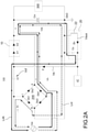
- FIG. 2A and FIG. 2B show a circuit diagram illustrating a current path when the filter circuit operates under a negative half cycle of an AC voltage and a circuit diagram illustrating a current path when the filter circuit operates under a positive half cycle of the AC voltage according to the present disclosure, respectively.
- the first current path is a negative half cycle harmonic compensation path Lnh
- the second current path is a negative half cycle rectifying path Lnr.
- Lnh negative half cycle harmonic compensation path
- Lnr negative half cycle rectifying path
- the first one is that the negative half cycle rectifying path Lnr is generated when the AC voltage Vac is greater than the DC voltage Vdc on the input capacitor Cin.
- the negative half cycle rectifying path Lnr is formed by the neutral wire end N of the AC voltage Vac, the bridge rectifying diode Db4, the positive end A, the input capacitor Cin, the negative end B, the bridge rectifying diode Db1, and the live wire end L of the AC voltage Vac.
- this current path is also the current path for the normal AC voltage Vac to charge the input capacitor Cin through the bridge rectifying circuit 200.
- the other current path is mainly provided by the filter circuit 100, which is the negative half cycle harmonic compensation path Lnh generated when the AC voltage Vac is greater than the DC voltage Vdc plus the voltage on the voltage stabilizing capacitor Cs (i.e., the voltage source Vs).
- the negative half cycle harmonic compensation path Lnh is formed by the neutral wire end N of the AC voltage Vac, the bridge rectifying diode Db4, the positive end A, the input capacitor Cin, the voltage stabilizing capacitor Cs, the unidirectional switch D, the freewheeling capacitor Cf, and the live wire end L of the AC voltage Vac.
- this current path is the current path of performing harmonic compensation to the negative half cycle of the input current Iin by the filter circuit 100.
- the AC waveform alternately changes in the positive half cycle and the negative half cycle over time.
- the negative half cycle harmonic compensation path Lnh since the capacitor voltage Vcf on the freewheeling capacitor Cf (i.e., a voltage across the freewheeling capacitor Cf) has been discharged in the previous cycle (i.e., a positive half cycle harmonic compensation path Lph is formed in the positive half cycle), no energy is stored in the freewheeling capacitor Cf. Therefore, when the negative half cycle harmonic compensation is performed, the voltage source Vs provided by the power generation circuit 20 charges the freewheeling capacitor Cf through the unidirectional switch D so that the capacitor voltage Vcf is established on the freewheeling capacitor Cf.
- the first current path is a positive half cycle harmonic compensation path Lph
- the second current path is a positive half cycle rectifying path Lpr.
- the first one is that the positive half cycle rectifying path Lpr is generated when the AC voltage Vac is greater than the DC voltage Vdc on the input capacitor Cin.
- the positive half cycle rectifying path Lpr is formed by the live wire end L of the AC voltage Vac, the bridge rectifying diode Db2, the positive end A, the input capacitor Cin, the negative end B, the bridge rectifying diode Db3, and the neutral wire end N of the AC voltage Vac.
- this current path is also the current path for the normal AC voltage Vac to charge the input capacitor Cin through the bridge rectifying circuit 200.
- the other current path is mainly provided by the filter circuit 100, which is the positive half cycle harmonic compensation path Lph generated when the AC voltage Vac plus the capacitor voltage Vcf on the freewheeling capacitor Cf is greater than the DC voltage Vdc.
- the positive half cycle harmonic compensation path Lph is formed by the live wire end L of the AC voltage Vac, the freewheeling capacitor Cf, the freewheeling switch 10, the input capacitor Cin, the negative end B, the bridge rectifying diode Db3, and the neutral wire end N of the AC voltage Vac.
- this current path is the current path of performing harmonic compensation to the positive half cycle of the input current Iin by the filter circuit 100.
- the capacitor voltage Vcf is established by the freewheeling capacitor Cf in the previous cycle (i.e., the negative half cycle harmonic compensation path Lnh is formed in the negative half cycle)
- the energy stored in the freewheeling capacitor Cf is released to the input capacitor Cin through the freewheeling switch 10 when the positive half cycle harmonic compensation is performed.
- the rear end of the input capacitor Cin does not need to be coupled to the expensive power factor corrector (PFC). It is only necessary to use the filter circuit 100 to make the current waveforms I and III as shown in FIG. 3 in the positive and negative half cycles of the AC voltage Vac, and the harmonic distortion can be improved. Moreover, it can selectively use only cheap and easily available passive electronic components to reduce circuit costs and improve harmonic distortion without using active control components and corresponding control technology.
- PFC power factor corrector
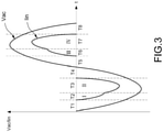
- FIG. 3 show schematic waveforms of the AC voltage and compensated input current according to the present disclosure, and also refer to FIG. 1 to FIG. 2B .
- the AC voltage Vac is in the negative half cycle, and since a voltage generated in the previous cycle (i.e., the positive half cycle of the AC voltage Vac) is established on the input capacitor Cin, no current path of the input current Iin is provided.
- the unidirectional switch D is not turned on, and the power generation circuit 20 only provides a voltage source Vs to maintain the stable operation of the controller IC.
- the freewheeling capacitor Cf has no stored energy (the stored energy has been discharged in the previous cycle), and since the voltage on the series-connected input capacitor Cin and the voltage stabilizing capacitor Cs (i.e., the DC voltage Vac plus the voltage source Vs) is less than the AC voltage Vac, the negative half cycle harmonic compensation path Lnh is provided to charge the freewheeling capacitor Cf so that the capacitor voltage Vcf is stablished on the freewheeling capacitor Cf.
- the freewheeling capacitor Cf has established the capacitor voltage Vcf, and therefore the negative half cycle harmonic compensation path Lnh is disconnected.
- a negative half cycle rectifying path Lnr is formed so that the AC voltage Vac charges the input capacitor Cin.
- the negative half cycle rectifying path Lnr is disconnected, and no current path of the input current Iin is provided.
- the voltage source Vs charges the freewheeling capacitor Cf so that a waveform I of a first compensation current is generated during the time period T2.
- the waveform I of the first compensation current just compensates a missing part of the input current Iin (i.e., the missing part of a negative half cycle rectifying current waveform II) before the negative half cycle rectifying path Lnr is formed. Therefore, the negative half cycle waveform of the compensated input current Iin (i.e., the waveform I plus the waveform II) is close to the negative half cycle waveform of the AC voltage Vac.
- the AC voltage Vac changes from the negative half cycle to the positive half cycle.
- a voltage generated in the previous cycle i.e., the negative half cycle of the AC voltage Vac
- no current path of the input current Iin is provided.
- the unidirectional switch D is not turned on, and the power generation circuit 20 only provides a voltage source Vs to maintain the stable operation of the controller IC.
- the stored energy of the freewheeling capacitor Cf is released to the input capacitor Cin so that a waveform III of a second compensation current is generated during the time period T6.
- the waveform III of the second compensation current just compensates a missing part of the input current Iin (i.e., the missing part of a positive half cycle rectifying current waveform IV) before the positive half cycle rectifying path Lpr is formed. Therefore, the positive half cycle waveform of the compensated input current Iin (i.e., the waveform III plus the waveform IV) is close to the positive half cycle waveform of the AC voltage Vac.
- the reason why the freewheeling switch 10 uses the first diode D1 in series with the second diode D2 is that a forward conduction voltage of the bridge rectifying diode Db1-Db4 is about 1 volt, and a forward conduction voltage of an ordinary diode is about 0.7 volts.
- the freewheeling switch 10 only uses a single diode, and the bridge rectifying diode Db2 between the live wire end L and the positive end A and the single diode of the freewheeling switch 10 are both forward biased (turned on), the voltage across the bridge rectifying diode Db2 will be greater than the voltage across the single diode of the freewheeling switch 10.
- the freewheeling switch 10 uses the first diode D1 in series with the second diode D2 to increase the voltage across the two diodes to about 1.4 volts, which is greater than the voltage across the bridge rectifying diode Db2 (about 1 volt). That is, a first conduction voltage, such as 1.4 volts of the freewheeling switch 10 will be greater than a second conduction voltage, such as 1 volt of the bridge rectifying diode Db2 between the live wire end L and the positive end A.
- the freewheeling capacitor Cf will not generate a negative voltage when the bridge rectifying diode Db2 and the freewheeling switch 10 are both forward biased (turned on), thereby increasing the compensation effect of the filter circuit 100 when performing harmonic compensation.
- the freewheeling switch 10 is not limited to a circuit structure in which the first diode D1 is connected to the second diode D2 in series. Any circuit structure and application that can ensure that the forward conduction voltage of the freewheeling switch 10 can be greater than the conduction voltage of the bridge rectifying diode Db1-Db4 (for example, by using a switch and its control technology) should be embraced within the scope of the present disclosure.
- the freewheeling switch 10 may choose a single diode whose condition voltage is greater than the conduction voltage of the bridge rectifying diode Db1-Db4, or use multiple diodes in series to make the total conduction voltage be greater than the conduction voltage of the bridge rectifying diode Db1-Db4, or any component whose conduction voltage is greater than the conduction voltage of the bridge rectifying diode Db1-Db4.
- the capacitance value of the voltage stabilizing capacitor Cs must be greater than the capacitance value of the freewheeling capacitor Cf, and it is better to use an electrolytic capacitor as the voltage stabilizing capacitor Cs.
- an electrolytic capacitor, a ceramic capacitor, or a tantalum capacitor may be used as the freewheeling capacitor Cf.
- the capacitance value of the freewheeling capacitor Cf will affect the current waveforms during the time periods T2 and T6 (i.e., the waveforms I and III).
- the capacitance value of the freewheeling capacitor Cf When the capacitance value of the freewheeling capacitor Cf is smaller, the energy can be stored and released is less so that the duration of the time periods T2 and T6 is shorter, and the waveforms I and III are steeper. Otherwise, the duration of the time periods T2 and T6 is longer, and the waveforms I and III are relatively gentle. Therefore, the capacitance value of the freewheeling capacitor Cf may be adjusted according to actual requirements to acquire different harmonic compensation effects of the filter circuit 100.
Landscapes
- Engineering & Computer Science (AREA)
- Power Engineering (AREA)
- Computer Networks & Wireless Communication (AREA)
- Rectifiers (AREA)
Applications Claiming Priority (1)
| Application Number | Priority Date | Filing Date | Title |
|---|---|---|---|
| CN202010914355.7A CN114142747B (zh) | 2020-09-03 | 2020-09-03 | 具有谐波补偿的滤波电路 |
Publications (2)
| Publication Number | Publication Date |
|---|---|
| EP3965276A1 true EP3965276A1 (fr) | 2022-03-09 |
| EP3965276B1 EP3965276B1 (fr) | 2023-07-05 |
Family
ID=75202995
Family Applications (1)
| Application Number | Title | Priority Date | Filing Date |
|---|---|---|---|
| EP21164285.5A Active EP3965276B1 (fr) | 2020-09-03 | 2021-03-23 | Circuit de filtre à compensation d'harmonique |
Country Status (3)
| Country | Link |
|---|---|
| EP (1) | EP3965276B1 (fr) |
| KR (1) | KR102571898B1 (fr) |
| CN (1) | CN114142747B (fr) |
Citations (4)
| Publication number | Priority date | Publication date | Assignee | Title |
|---|---|---|---|---|
| EP0377510A2 (fr) * | 1989-01-05 | 1990-07-11 | General Electric Company | Circuit de compensation de facteur de puissance |
| EP1033806A2 (fr) * | 1999-02-17 | 2000-09-06 | Matsushita Electric Industrial Co., Ltd. | Alimentation de puissance electric |
| CN201131076Y (zh) * | 2007-12-24 | 2008-10-08 | 樊贤信 | 新型高压钠灯电子镇流器 |
| US20130194838A1 (en) * | 2012-01-31 | 2013-08-01 | Delta Electronics Inc. | Three-phase soft-switched pfc rectifiers |
Family Cites Families (5)
| Publication number | Priority date | Publication date | Assignee | Title |
|---|---|---|---|---|
| JPH08205519A (ja) * | 1995-01-20 | 1996-08-09 | Ricoh Co Ltd | スイッチングレギュレータ |
| JP3726611B2 (ja) * | 2000-01-17 | 2005-12-14 | 松下電器産業株式会社 | 空気調和機の電源回路 |
| JP3740926B2 (ja) * | 2000-01-26 | 2006-02-01 | 松下電器産業株式会社 | 電源装置 |
| CN102664517B (zh) * | 2012-05-08 | 2014-09-17 | 英飞特电子(杭州)股份有限公司 | 一种功率因数校正电路 |
| TWI726085B (zh) * | 2017-04-05 | 2021-05-01 | 晶元光電股份有限公司 | 發光二極體之驅動器 |
-
2020
- 2020-09-03 CN CN202010914355.7A patent/CN114142747B/zh active Active
-
2021
- 2021-03-23 EP EP21164285.5A patent/EP3965276B1/fr active Active
- 2021-04-19 KR KR1020210050461A patent/KR102571898B1/ko active Active
Patent Citations (4)
| Publication number | Priority date | Publication date | Assignee | Title |
|---|---|---|---|---|
| EP0377510A2 (fr) * | 1989-01-05 | 1990-07-11 | General Electric Company | Circuit de compensation de facteur de puissance |
| EP1033806A2 (fr) * | 1999-02-17 | 2000-09-06 | Matsushita Electric Industrial Co., Ltd. | Alimentation de puissance electric |
| CN201131076Y (zh) * | 2007-12-24 | 2008-10-08 | 樊贤信 | 新型高压钠灯电子镇流器 |
| US20130194838A1 (en) * | 2012-01-31 | 2013-08-01 | Delta Electronics Inc. | Three-phase soft-switched pfc rectifiers |
Also Published As
| Publication number | Publication date |
|---|---|
| CN114142747A (zh) | 2022-03-04 |
| KR102571898B1 (ko) | 2023-08-28 |
| KR20220030867A (ko) | 2022-03-11 |
| CN114142747B (zh) | 2025-08-08 |
| EP3965276B1 (fr) | 2023-07-05 |
Similar Documents
| Publication | Publication Date | Title |
|---|---|---|
| CN109247081B (zh) | 半桥谐振转换器、使用它们的电路、以及对应的控制方法 | |
| EP3437178B1 (fr) | Convertisseur ca/cc à pfc utilisant un convertisseur résonnant en demi-pont, et procédé de conversion correspondant | |
| US10003254B2 (en) | Digital AC/DC power converter | |
| US6184630B1 (en) | Electronic lamp ballast with voltage source power feedback to AC-side | |
| US9030049B2 (en) | Alternating current (AC) to direct current (DC) converter device | |
| CN109661072B (zh) | Llc谐振变换器、led驱动电路及其控制方法 | |
| US11509238B2 (en) | AC/DC power supply, rectifier circuit and control method | |
| JP2006519577A (ja) | 単段力率補正及び電力変換回路 | |
| EP4101263A1 (fr) | Onduleur résonant et procédé de conversion | |
| CN119325685A (zh) | 转换器装置 | |
| TW201929381A (zh) | 不斷電電源供應裝置 | |
| US6396724B1 (en) | Charge-pumped DC bias supply | |
| CN101127483B (zh) | 应用于场发射显示器的电源供应器 | |
| US20150085535A1 (en) | LLC single stage power factor correction converter | |
| US6819575B1 (en) | AC/DC switch mode power supply with power factor correction using direct energy transfer concept | |
| EP3965276A1 (fr) | Circuit de filtre à compensation d'harmonique | |
| CN112689363A (zh) | 电源转换器 | |
| CN109412452B (zh) | 一种直流交流电源变换电路 | |
| TWI725915B (zh) | 具有諧波補償之濾波電路 | |
| CN214281232U (zh) | 闪光灯的电源控制设备及闪光灯的供电设备 | |
| CN111052576A (zh) | 具有减小的体电容的供电系统 | |
| CN211296552U (zh) | 一种直流输入推挽型正负高压发生器的控制电路 | |
| US20090116264A1 (en) | Power supply circuit with voltage converting circuits and control method therefor | |
| CN107617806B (zh) | 焊机控制电路 | |
| Davis et al. | Developed non-isolated high step-up converter with low voltage stress |
Legal Events
| Date | Code | Title | Description |
|---|---|---|---|
| PUAI | Public reference made under article 153(3) epc to a published international application that has entered the european phase |
Free format text: ORIGINAL CODE: 0009012 |
|
| STAA | Information on the status of an ep patent application or granted ep patent |
Free format text: STATUS: THE APPLICATION HAS BEEN PUBLISHED |
|
| AK | Designated contracting states |
Kind code of ref document: A1 Designated state(s): AL AT BE BG CH CY CZ DE DK EE ES FI FR GB GR HR HU IE IS IT LI LT LU LV MC MK MT NL NO PL PT RO RS SE SI SK SM TR |
|
| STAA | Information on the status of an ep patent application or granted ep patent |
Free format text: STATUS: REQUEST FOR EXAMINATION WAS MADE |
|
| 17P | Request for examination filed |
Effective date: 20220330 |
|
| RBV | Designated contracting states (corrected) |
Designated state(s): AL AT BE BG CH CY CZ DE DK EE ES FI FR GB GR HR HU IE IS IT LI LT LU LV MC MK MT NL NO PL PT RO RS SE SI SK SM TR |
|
| GRAP | Despatch of communication of intention to grant a patent |
Free format text: ORIGINAL CODE: EPIDOSNIGR1 |
|
| STAA | Information on the status of an ep patent application or granted ep patent |
Free format text: STATUS: GRANT OF PATENT IS INTENDED |
|
| INTG | Intention to grant announced |
Effective date: 20230202 |
|
| RAP3 | Party data changed (applicant data changed or rights of an application transferred) |
Owner name: DELTA ELECTRONICS, INC. |
|
| GRAS | Grant fee paid |
Free format text: ORIGINAL CODE: EPIDOSNIGR3 |
|
| GRAA | (expected) grant |
Free format text: ORIGINAL CODE: 0009210 |
|
| STAA | Information on the status of an ep patent application or granted ep patent |
Free format text: STATUS: THE PATENT HAS BEEN GRANTED |
|
| AK | Designated contracting states |
Kind code of ref document: B1 Designated state(s): AL AT BE BG CH CY CZ DE DK EE ES FI FR GB GR HR HU IE IS IT LI LT LU LV MC MK MT NL NO PL PT RO RS SE SI SK SM TR |
|
| REG | Reference to a national code |
Ref country code: CH Ref legal event code: EP |
|
| REG | Reference to a national code |
Ref country code: AT Ref legal event code: REF Ref document number: 1585735 Country of ref document: AT Kind code of ref document: T Effective date: 20230715 |
|
| REG | Reference to a national code |
Ref country code: DE Ref legal event code: R096 Ref document number: 602021003204 Country of ref document: DE |
|
| REG | Reference to a national code |
Ref country code: IE Ref legal event code: FG4D |
|
| REG | Reference to a national code |
Ref country code: NL Ref legal event code: FP |
|
| REG | Reference to a national code |
Ref country code: LT Ref legal event code: MG9D |
|
| REG | Reference to a national code |
Ref country code: AT Ref legal event code: MK05 Ref document number: 1585735 Country of ref document: AT Kind code of ref document: T Effective date: 20230705 |
|
| PG25 | Lapsed in a contracting state [announced via postgrant information from national office to epo] |
Ref country code: GR Free format text: LAPSE BECAUSE OF FAILURE TO SUBMIT A TRANSLATION OF THE DESCRIPTION OR TO PAY THE FEE WITHIN THE PRESCRIBED TIME-LIMIT Effective date: 20231006 |
|
| PG25 | Lapsed in a contracting state [announced via postgrant information from national office to epo] |
Ref country code: ES Free format text: LAPSE BECAUSE OF FAILURE TO SUBMIT A TRANSLATION OF THE DESCRIPTION OR TO PAY THE FEE WITHIN THE PRESCRIBED TIME-LIMIT Effective date: 20230705 |
|
| PG25 | Lapsed in a contracting state [announced via postgrant information from national office to epo] |
Ref country code: IS Free format text: LAPSE BECAUSE OF FAILURE TO SUBMIT A TRANSLATION OF THE DESCRIPTION OR TO PAY THE FEE WITHIN THE PRESCRIBED TIME-LIMIT Effective date: 20231105 |
|
| PG25 | Lapsed in a contracting state [announced via postgrant information from national office to epo] |
Ref country code: SE Free format text: LAPSE BECAUSE OF FAILURE TO SUBMIT A TRANSLATION OF THE DESCRIPTION OR TO PAY THE FEE WITHIN THE PRESCRIBED TIME-LIMIT Effective date: 20230705 Ref country code: RS Free format text: LAPSE BECAUSE OF FAILURE TO SUBMIT A TRANSLATION OF THE DESCRIPTION OR TO PAY THE FEE WITHIN THE PRESCRIBED TIME-LIMIT Effective date: 20230705 Ref country code: PT Free format text: LAPSE BECAUSE OF FAILURE TO SUBMIT A TRANSLATION OF THE DESCRIPTION OR TO PAY THE FEE WITHIN THE PRESCRIBED TIME-LIMIT Effective date: 20231106 Ref country code: NO Free format text: LAPSE BECAUSE OF FAILURE TO SUBMIT A TRANSLATION OF THE DESCRIPTION OR TO PAY THE FEE WITHIN THE PRESCRIBED TIME-LIMIT Effective date: 20231005 Ref country code: LV Free format text: LAPSE BECAUSE OF FAILURE TO SUBMIT A TRANSLATION OF THE DESCRIPTION OR TO PAY THE FEE WITHIN THE PRESCRIBED TIME-LIMIT Effective date: 20230705 Ref country code: LT Free format text: LAPSE BECAUSE OF FAILURE TO SUBMIT A TRANSLATION OF THE DESCRIPTION OR TO PAY THE FEE WITHIN THE PRESCRIBED TIME-LIMIT Effective date: 20230705 Ref country code: IS Free format text: LAPSE BECAUSE OF FAILURE TO SUBMIT A TRANSLATION OF THE DESCRIPTION OR TO PAY THE FEE WITHIN THE PRESCRIBED TIME-LIMIT Effective date: 20231105 Ref country code: HR Free format text: LAPSE BECAUSE OF FAILURE TO SUBMIT A TRANSLATION OF THE DESCRIPTION OR TO PAY THE FEE WITHIN THE PRESCRIBED TIME-LIMIT Effective date: 20230705 Ref country code: GR Free format text: LAPSE BECAUSE OF FAILURE TO SUBMIT A TRANSLATION OF THE DESCRIPTION OR TO PAY THE FEE WITHIN THE PRESCRIBED TIME-LIMIT Effective date: 20231006 Ref country code: FI Free format text: LAPSE BECAUSE OF FAILURE TO SUBMIT A TRANSLATION OF THE DESCRIPTION OR TO PAY THE FEE WITHIN THE PRESCRIBED TIME-LIMIT Effective date: 20230705 Ref country code: ES Free format text: LAPSE BECAUSE OF FAILURE TO SUBMIT A TRANSLATION OF THE DESCRIPTION OR TO PAY THE FEE WITHIN THE PRESCRIBED TIME-LIMIT Effective date: 20230705 Ref country code: AT Free format text: LAPSE BECAUSE OF FAILURE TO SUBMIT A TRANSLATION OF THE DESCRIPTION OR TO PAY THE FEE WITHIN THE PRESCRIBED TIME-LIMIT Effective date: 20230705 |
|
| PG25 | Lapsed in a contracting state [announced via postgrant information from national office to epo] |
Ref country code: PL Free format text: LAPSE BECAUSE OF FAILURE TO SUBMIT A TRANSLATION OF THE DESCRIPTION OR TO PAY THE FEE WITHIN THE PRESCRIBED TIME-LIMIT Effective date: 20230705 |
|
| REG | Reference to a national code |
Ref country code: DE Ref legal event code: R097 Ref document number: 602021003204 Country of ref document: DE |
|
| PG25 | Lapsed in a contracting state [announced via postgrant information from national office to epo] |
Ref country code: SM Free format text: LAPSE BECAUSE OF FAILURE TO SUBMIT A TRANSLATION OF THE DESCRIPTION OR TO PAY THE FEE WITHIN THE PRESCRIBED TIME-LIMIT Effective date: 20230705 Ref country code: RO Free format text: LAPSE BECAUSE OF FAILURE TO SUBMIT A TRANSLATION OF THE DESCRIPTION OR TO PAY THE FEE WITHIN THE PRESCRIBED TIME-LIMIT Effective date: 20230705 Ref country code: EE Free format text: LAPSE BECAUSE OF FAILURE TO SUBMIT A TRANSLATION OF THE DESCRIPTION OR TO PAY THE FEE WITHIN THE PRESCRIBED TIME-LIMIT Effective date: 20230705 Ref country code: DK Free format text: LAPSE BECAUSE OF FAILURE TO SUBMIT A TRANSLATION OF THE DESCRIPTION OR TO PAY THE FEE WITHIN THE PRESCRIBED TIME-LIMIT Effective date: 20230705 Ref country code: CZ Free format text: LAPSE BECAUSE OF FAILURE TO SUBMIT A TRANSLATION OF THE DESCRIPTION OR TO PAY THE FEE WITHIN THE PRESCRIBED TIME-LIMIT Effective date: 20230705 Ref country code: SK Free format text: LAPSE BECAUSE OF FAILURE TO SUBMIT A TRANSLATION OF THE DESCRIPTION OR TO PAY THE FEE WITHIN THE PRESCRIBED TIME-LIMIT Effective date: 20230705 |
|
| PLBE | No opposition filed within time limit |
Free format text: ORIGINAL CODE: 0009261 |
|
| STAA | Information on the status of an ep patent application or granted ep patent |
Free format text: STATUS: NO OPPOSITION FILED WITHIN TIME LIMIT |
|
| 26N | No opposition filed |
Effective date: 20240408 |
|
| PG25 | Lapsed in a contracting state [announced via postgrant information from national office to epo] |
Ref country code: SI Free format text: LAPSE BECAUSE OF FAILURE TO SUBMIT A TRANSLATION OF THE DESCRIPTION OR TO PAY THE FEE WITHIN THE PRESCRIBED TIME-LIMIT Effective date: 20230705 |
|
| REG | Reference to a national code |
Ref country code: CH Ref legal event code: PL |
|
| PG25 | Lapsed in a contracting state [announced via postgrant information from national office to epo] |
Ref country code: BG Free format text: LAPSE BECAUSE OF FAILURE TO SUBMIT A TRANSLATION OF THE DESCRIPTION OR TO PAY THE FEE WITHIN THE PRESCRIBED TIME-LIMIT Effective date: 20230705 |
|
| PG25 | Lapsed in a contracting state [announced via postgrant information from national office to epo] |
Ref country code: LU Free format text: LAPSE BECAUSE OF NON-PAYMENT OF DUE FEES Effective date: 20240323 |
|
| PG25 | Lapsed in a contracting state [announced via postgrant information from national office to epo] |
Ref country code: MC Free format text: LAPSE BECAUSE OF FAILURE TO SUBMIT A TRANSLATION OF THE DESCRIPTION OR TO PAY THE FEE WITHIN THE PRESCRIBED TIME-LIMIT Effective date: 20230705 |
|
| PG25 | Lapsed in a contracting state [announced via postgrant information from national office to epo] |
Ref country code: MC Free format text: LAPSE BECAUSE OF FAILURE TO SUBMIT A TRANSLATION OF THE DESCRIPTION OR TO PAY THE FEE WITHIN THE PRESCRIBED TIME-LIMIT Effective date: 20230705 Ref country code: LU Free format text: LAPSE BECAUSE OF NON-PAYMENT OF DUE FEES Effective date: 20240323 Ref country code: BG Free format text: LAPSE BECAUSE OF FAILURE TO SUBMIT A TRANSLATION OF THE DESCRIPTION OR TO PAY THE FEE WITHIN THE PRESCRIBED TIME-LIMIT Effective date: 20230705 |
|
| REG | Reference to a national code |
Ref country code: BE Ref legal event code: MM Effective date: 20240331 |
|
| PG25 | Lapsed in a contracting state [announced via postgrant information from national office to epo] |
Ref country code: BE Free format text: LAPSE BECAUSE OF NON-PAYMENT OF DUE FEES Effective date: 20240331 |
|
| PG25 | Lapsed in a contracting state [announced via postgrant information from national office to epo] |
Ref country code: IE Free format text: LAPSE BECAUSE OF NON-PAYMENT OF DUE FEES Effective date: 20240323 |
|
| PG25 | Lapsed in a contracting state [announced via postgrant information from national office to epo] |
Ref country code: IE Free format text: LAPSE BECAUSE OF NON-PAYMENT OF DUE FEES Effective date: 20240323 Ref country code: BE Free format text: LAPSE BECAUSE OF NON-PAYMENT OF DUE FEES Effective date: 20240331 Ref country code: CH Free format text: LAPSE BECAUSE OF NON-PAYMENT OF DUE FEES Effective date: 20240331 |
|
| PG25 | Lapsed in a contracting state [announced via postgrant information from national office to epo] |
Ref country code: CY Free format text: LAPSE BECAUSE OF FAILURE TO SUBMIT A TRANSLATION OF THE DESCRIPTION OR TO PAY THE FEE WITHIN THE PRESCRIBED TIME-LIMIT; INVALID AB INITIO Effective date: 20210323 |
|
| PG25 | Lapsed in a contracting state [announced via postgrant information from national office to epo] |
Ref country code: HU Free format text: LAPSE BECAUSE OF FAILURE TO SUBMIT A TRANSLATION OF THE DESCRIPTION OR TO PAY THE FEE WITHIN THE PRESCRIBED TIME-LIMIT; INVALID AB INITIO Effective date: 20210323 |
|
| GBPC | Gb: european patent ceased through non-payment of renewal fee |
Effective date: 20250323 |
|
| PG25 | Lapsed in a contracting state [announced via postgrant information from national office to epo] |
Ref country code: TR Free format text: LAPSE BECAUSE OF FAILURE TO SUBMIT A TRANSLATION OF THE DESCRIPTION OR TO PAY THE FEE WITHIN THE PRESCRIBED TIME-LIMIT Effective date: 20230705 |
|
| PG25 | Lapsed in a contracting state [announced via postgrant information from national office to epo] |
Ref country code: GB Free format text: LAPSE BECAUSE OF NON-PAYMENT OF DUE FEES Effective date: 20250323 |
|
| PGFP | Annual fee paid to national office [announced via postgrant information from national office to epo] |
Ref country code: NL Payment date: 20260213 Year of fee payment: 6 |
|
| PGFP | Annual fee paid to national office [announced via postgrant information from national office to epo] |
Ref country code: DE Payment date: 20260128 Year of fee payment: 6 |
|
| PGFP | Annual fee paid to national office [announced via postgrant information from national office to epo] |
Ref country code: IT Payment date: 20260220 Year of fee payment: 6 |
|
| PGFP | Annual fee paid to national office [announced via postgrant information from national office to epo] |
Ref country code: FR Payment date: 20260209 Year of fee payment: 6 |