EP1033806A2 - Alimentation de puissance electric - Google Patents
Alimentation de puissance electric Download PDFInfo
- Publication number
- EP1033806A2 EP1033806A2 EP00103034A EP00103034A EP1033806A2 EP 1033806 A2 EP1033806 A2 EP 1033806A2 EP 00103034 A EP00103034 A EP 00103034A EP 00103034 A EP00103034 A EP 00103034A EP 1033806 A2 EP1033806 A2 EP 1033806A2
- Authority
- EP
- European Patent Office
- Prior art keywords
- capacitor
- switching means
- electric power
- power supply
- rectifier circuit
- Prior art date
- Legal status (The legal status is an assumption and is not a legal conclusion. Google has not performed a legal analysis and makes no representation as to the accuracy of the status listed.)
- Granted
Links
Images


Classifications
-
- H—ELECTRICITY
- H02—GENERATION; CONVERSION OR DISTRIBUTION OF ELECTRIC POWER
- H02M—APPARATUS FOR CONVERSION BETWEEN AC AND AC, BETWEEN AC AND DC, OR BETWEEN DC AND DC, AND FOR USE WITH MAINS OR SIMILAR POWER SUPPLY SYSTEMS; CONVERSION OF DC OR AC INPUT POWER INTO SURGE OUTPUT POWER; CONTROL OR REGULATION THEREOF
- H02M1/00—Details of apparatus for conversion
- H02M1/42—Circuits or arrangements for compensating for or adjusting power factor in converters or inverters
- H02M1/4208—Arrangements for improving power factor of AC input
- H02M1/4266—Arrangements for improving power factor of AC input using passive elements
-
- Y—GENERAL TAGGING OF NEW TECHNOLOGICAL DEVELOPMENTS; GENERAL TAGGING OF CROSS-SECTIONAL TECHNOLOGIES SPANNING OVER SEVERAL SECTIONS OF THE IPC; TECHNICAL SUBJECTS COVERED BY FORMER USPC CROSS-REFERENCE ART COLLECTIONS [XRACs] AND DIGESTS
- Y02—TECHNOLOGIES OR APPLICATIONS FOR MITIGATION OR ADAPTATION AGAINST CLIMATE CHANGE
- Y02B—CLIMATE CHANGE MITIGATION TECHNOLOGIES RELATED TO BUILDINGS, e.g. HOUSING, HOUSE APPLIANCES OR RELATED END-USER APPLICATIONS
- Y02B70/00—Technologies for an efficient end-user side electric power management and consumption
- Y02B70/10—Technologies improving the efficiency by using switched-mode power supplies [SMPS], i.e. efficient power electronics conversion e.g. power factor correction or reduction of losses in power supplies or efficient standby modes
-
- Y—GENERAL TAGGING OF NEW TECHNOLOGICAL DEVELOPMENTS; GENERAL TAGGING OF CROSS-SECTIONAL TECHNOLOGIES SPANNING OVER SEVERAL SECTIONS OF THE IPC; TECHNICAL SUBJECTS COVERED BY FORMER USPC CROSS-REFERENCE ART COLLECTIONS [XRACs] AND DIGESTS
- Y02—TECHNOLOGIES OR APPLICATIONS FOR MITIGATION OR ADAPTATION AGAINST CLIMATE CHANGE
- Y02P—CLIMATE CHANGE MITIGATION TECHNOLOGIES IN THE PRODUCTION OR PROCESSING OF GOODS
- Y02P80/00—Climate change mitigation technologies for sector-wide applications
- Y02P80/10—Efficient use of energy, e.g. using compressed air or pressurized fluid as energy carrier
Definitions
- the present invention relates to an electric power supply using rectification with a bridge rectifier circuit to supply electric power to devices and systems.
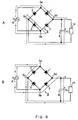
- FIGs. 6A and 6B show an example of a full-wave rectifier circuit using a bridge rectifier circuit.
- the full-wave rectifier circuit shown in this drawing includes a bridge rectifier circuit having four diodes 1 to 4.
- Numeral 14 denotes a load.
- Fig. 6A illustrates the flow of current during the positive half cycle of the ac power source 6. As indicated by the arrows, the current flows through the diode 1, a smoothing capacitor 8, and the diode 4, in that order, so that a positive voltage V O can be given out.
- Fig. 6B illustrates the flow of current during the negative half cycle of the ac power source 6. As indicated by the arrows, the current flows through the diode 3, the smoothing capacitor 8, and the diode 2, in that order, so that a positive voltage V O can be given out. In other words, the full wave of the alternating input from the ac power source 6 is rectified, and a positive dc voltage can be attained.
- the power factor is low, because an input current flows only during the period when the voltage of the ac power source 6 is higher than the dc output voltage, and there is also the problem of higher harmonics in the power supply.
- a reactor is connected between the ac power supply 6 and the bridge rectifier circuit 5, but although this method can suppress higher harmonics, a power factor of only about 70% can be attained, so that there is the problem that the components for medium to large power supplies are big, which leads not only to bigger devices, but also to a larger load on the power system.
- an electric power supply of the present invention includes an ac power source; a bridge rectifier circuit having four diodes for full-wave rectifying an alternating current produced with the ac power source; a smoothing capacitor connected to dc output terminals of the bridge rectifier circuit.
- a reactor connected between the ac power source and ac input terminal of the bridge rectifier circuit.
- a capacitor connected between an ac input terminal and a dc output terminal of the bridge rectifier circuit.
- the reactor forms a serial resonance circuit with the capacitor or the smoothing capacitor, so that the output waveforms are smoothened, and higher harmonics are suppressed.
- the inductance of the reactor and the static capacitance of the capacitor are selected such that during a half-cycle of ac current from the ac power source, a resonance current flows through the reactor and the capacitor and charges the capacitor, and a voltage V C across the capacitor rises from zero to an output voltage V O of the bridge rectifier circuit; and ac current from the ac power source discharges the capacitor during the next half-cycle so that the voltage V C decreases from V O to zero.
- the capacitor is connected between an ac input terminal of the bridge rectifier circuit and a positive dc output terminal.
- the capacitor is connected between an ac input terminal of the bridge rectifier circuit and a negative dc output terminal.
- a switching means that opens when the load is small is connected between the capacitor and a dc output terminal of the bridge rectifier circuit; and a diode is connected in parallel to the switching means, such that the diode blocks a charging of the capacitor.
- the switching means is connected between the capacitor and a negative dc output terminal of the bridge rectifier circuit; and the cathode of the diode connected in parallel to the switching means is connected to the side of the ac power source, and the anode of the diode connected in parallel to the switching means is connected to the negative dc output terminal.
- the switching means is connected between the capacitor and a positive dc output terminal of the bridge rectifier circuit; and the anode of the diode connected in parallel to the switching means is connected to the side of the ac power source, and the cathode of the diode connected in parallel to the switching means is connected to the side of the dc output terminal.
- the switching means opens and closes depending on an output voltage, an output current or an operating time of the load.
- the switching means and the diode connected in parallel to the switching means are realized as a MOSFET. With such an electric power supply, the number of components can be reduced, allowing miniaturization and reducing costs.
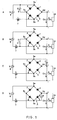
- Figs. 1A to D are circuit diagrams of electric power supplies in accordance with a first embodiment of the present invention.
- the electric power supplies shown in Figs. 1A to D include a bridge rectifier circuit 5 made of four diodes 1 to 4, and an ac power source 6.
- a reactor 7 is connected between the ac power source 6 and an ac input terminal of the bridge rectifier circuit 5.
- a capacitor 9 is connected between an ac input terminal and a dc output terminal of the bridge rectifier circuit.
- the capacitor 9 is connected between either the ac input terminal 5a or 5b and the negative dc output terminal 5c of the bridge rectifier circuit 5.
- the capacitor 9 is connected between either the ac input terminal 5a or 5b and the positive dc output terminal 5d of the bridge rectifier circuit 5.
- a smoothing capacitor 8 is connected between the positive dc output terminal 5d and the negative dc output terminal 5c of the bridge rectifier circuit 5. This smoothing capacitor 8 smoothens the strong ripples of the dc current obtained with the bridge rectifier circuit 5, thus producing a smooth dc current.
- Figs. 2A to 2D the following explains how the electric power supply shown in Fig. 1A operates.
- Figs. 2A and 2B illustrate the positive half cycle of the ac input voltage V i
- Figs. 2C and 2D illustrate the negative half cycle of the ac input voltage V i
- Fig. 3A illustrates the ac input voltage V i , the current I L flowing through the reactor 7 (ac input current), and the dc output voltage V O .
- Fig. 3B illustrates the ac input voltage V i , the current I C flowing though the capacitor 9, and the voltage V C across the capacitor 9.
- the abscissa marks time, and a horizontal interval between two neighboring broken lines corresponds to 3.33ms.
- the ordinate marks voltage and current, and a vertical interval between two neighboring broken lines corresponds to 100V or 5A.
- FIG. 2B shows the flow of the current after V C has increased to V O .
- V C is clamped at V O , so that the current flows in the direction indicated by the arrow "b" from the ac power source 6 through the diode 1, the smoothing capacitor 8, the diode 4 and the reactor 7 in that order.
- the reactor current I L when the current flows in the direction "b" corresponds to the portion marked L 2 in Fig. 3A.
- Fig. 2C shows the situation when the polarity of the ac power source 6 has reversed from that shown in Figs. 2A and B.
- the current flows from the ac power source 6 through the reactor 7, the diode 3, the smoothing capacitor 8, and the capacitor 9 in that order, as indicated by the arrow "c".
- the potential of the ac power source 6 is increased by the voltage V C across the capacitor 9, a current will flow through the smoothing capacitor 8 right from the zero crossing.
- the capacitor 9 With a current flow as shown in this drawing, the capacitor 9 continues to be discharged, and finally V C reaches zero.
- the reactance current I L while the capacitor 9 is being discharged corresponds to the portion marked L 3 in Fig. 3A, and the capacitor current I C corresponds to the portion marked C 2 in Fig. 3B.
- Fig. 2D shows the situation after the capacitor 7 has been completely discharged.
- the reactor current I L corresponds to the portion marked L 4 in Fig. 3A.
- V C is clamped at 0, so that the current again flows in the direction of the arrow "a" as shown in Fig. 2A.
- the potential of the ac power source 6 is increased by the voltage V C across the capacitor 9, so that a current will flow right from the zero crossing.
- the current from the ac power source 6 flows right from the zero crossing of the input voltage, which improves the power factor.
- Fig. 3C shows an example comparing higher harmonic components of the current with the national guidelines 15 for higher harmonics regulations.
- the abscissa marks the order of the higher harmonics
- the ordinate marks the current (wherein the interval between two neighboring broken lines corresponds to 0.5A).
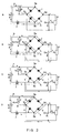
- Fig. 4 shows circuit diagrams of electric power supplies in accordance with a second embodiment of the present invention.
- the electric power supplies shown in Figs. 4A to 4D include a diode and a switching means in addition to the components included in the electric power supply shown in Figs. 1A to 1D.
- the potential of the ac power source 6 is increased by the voltage V C across the capacitor 9 in the situation shown in Fig. 2C. Therefore, when a small load is applied, the output voltage sometimes rises too high.
- a diode and a switching means are added, and for small loads below a certain value, the switching means is opened to stop the charging of the capacitor 9, which suppresses an increase of the output voltage.
- a diode 10 is connected between the negative dc output terminal 5c of the bridge rectifier circuit 5 and the capacitor 9.
- the cathode of the diode 10 is connected to the side of the ac power source 6, and the anode of the diode 10 is connected to the negative dc output terminal 5c.
- a switching means 11 is connected in parallel to the diode 10.
- the switching means 11 opens or closes depending on the size of the load. When the load is a small load below a certain value, the switching means 11 opens.
- the diode 10 which is connected so as to block the resonance current, stops the charging of the capacitor 9, so that an excessive increase of the output voltage can be prevented.
- a relay can be used, for example.
- Detecting the load can be performed, for example, by measuring the output voltage, the load current, or the operating time of the load. In devices using a motor, it is also possible to measure the output number of revolutions of the motor.
- the switching means 11 is opened by cutting off the current to the relay when the output voltage increases to a certain limit, and when the output voltage decreases below a certain lower limit, a current is sent through the relay, and the switching means 11 closes.
- the output voltage can be kept between a certain upper limit and a certain lower limit.
- a diode 10 and a switching means 11 are connected to the negative dc output terminal 5c of the bridge rectifier circuit 5 in the circuit shown in 1B.
- the connection and the operation are the same as for the circuit shown in 4A.
- circuits shown in Figs. 4C and 4D have the diode 10 and the switching means 11 added to the circuits shown in Figs. 1C and 1D, but they are different from the circuits in Figs. 4A and 4B in that the diode 10 and the switching means 11 are connected to the positive dc output terminal 5d. Their operation is the same as that of the circuits shown in Figs. 4A and 4B.
- Fig. 5 is a circuit diagram of an electric power supply in accordance with the third embodiment of the present invention.
- the electric power supply in Fig. 5 uses a MOSFET as the switching means for the electric power supply shown in Fig. 4.
- the MOSFET 12 is connected between the negative dc output terminal 5c of the bridge rectifier circuit 5 and the capacitor 9.
- a diode 13 is integrated with the MOSFET 12, its cathode being on the side of the ac power source 6, and its anode being on the side of the dc output terminal 5c.
- the parallel circuits of diode and switching means shown in Figs. 4A to 4D can be replaced with one MOSFET, so that the number of components can be reduced, which allows for miniaturization and cost cutting.
Landscapes
- Engineering & Computer Science (AREA)
- Power Engineering (AREA)
- Rectifiers (AREA)
- Dc-Dc Converters (AREA)
Applications Claiming Priority (2)
| Application Number | Priority Date | Filing Date | Title |
|---|---|---|---|
| JP03851399A JP3377959B2 (ja) | 1999-02-17 | 1999-02-17 | 電源装置 |
| JP3851399 | 1999-02-17 |
Publications (3)
| Publication Number | Publication Date |
|---|---|
| EP1033806A2 true EP1033806A2 (fr) | 2000-09-06 |
| EP1033806A3 EP1033806A3 (fr) | 2001-11-21 |
| EP1033806B1 EP1033806B1 (fr) | 2003-04-16 |
Family
ID=12527363
Family Applications (1)
| Application Number | Title | Priority Date | Filing Date |
|---|---|---|---|
| EP00103034A Expired - Lifetime EP1033806B1 (fr) | 1999-02-17 | 2000-02-15 | Alimentation de puissance electric |
Country Status (4)
| Country | Link |
|---|---|
| EP (1) | EP1033806B1 (fr) |
| JP (1) | JP3377959B2 (fr) |
| CN (1) | CN1143426C (fr) |
| ES (1) | ES2193016T3 (fr) |
Cited By (4)
| Publication number | Priority date | Publication date | Assignee | Title |
|---|---|---|---|---|
| WO2002060044A1 (fr) * | 2001-01-26 | 2002-08-01 | Matsushita Electric Industrial Co., Ltd. | Dispositif de puissance |
| EP1432109A4 (fr) * | 2001-09-28 | 2012-04-04 | Panasonic Corp | Source d'alimentation en energie |
| WO2020193268A1 (fr) * | 2019-03-23 | 2020-10-01 | Leopold Kostal Gmbh & Co. Kg | Convertisseur continu-continu isolé équipé d'un redresseur à pont de diodes complet côté secondaire et d'un condensateur auxiliaire asymétrique |
| EP3965276A1 (fr) * | 2020-09-03 | 2022-03-09 | Delta Electronics, Inc. | Circuit de filtre à compensation d'harmonique |
Families Citing this family (2)
| Publication number | Priority date | Publication date | Assignee | Title |
|---|---|---|---|---|
| JP3687641B2 (ja) | 2002-10-01 | 2005-08-24 | 松下電器産業株式会社 | インバ−タエアコン |
| WO2014086005A1 (fr) * | 2012-12-05 | 2014-06-12 | 中国北车股份有限公司大连电力牵引研发中心 | Appareil de traction à redresseur et unités diesel multiples |
Family Cites Families (2)
| Publication number | Priority date | Publication date | Assignee | Title |
|---|---|---|---|---|
| IT1257981B (it) * | 1991-09-27 | 1996-02-19 | Paolo Tenti | Dispositivo di conversione elettrica monostadio. |
| FR2724507B1 (fr) * | 1994-09-12 | 1996-12-13 | Oldham France Sa | Circuit redresseur de tension alternative |
-
1999
- 1999-02-17 JP JP03851399A patent/JP3377959B2/ja not_active Expired - Fee Related
-
2000
- 2000-02-15 EP EP00103034A patent/EP1033806B1/fr not_active Expired - Lifetime
- 2000-02-15 ES ES00103034T patent/ES2193016T3/es not_active Expired - Lifetime
- 2000-02-17 CN CNB00102373XA patent/CN1143426C/zh not_active Expired - Fee Related
Cited By (6)
| Publication number | Priority date | Publication date | Assignee | Title |
|---|---|---|---|---|
| WO2002060044A1 (fr) * | 2001-01-26 | 2002-08-01 | Matsushita Electric Industrial Co., Ltd. | Dispositif de puissance |
| US6671192B2 (en) | 2001-01-26 | 2003-12-30 | Matsushita Electric Industrial Co., Ltd. | Power apparatus |
| EP1432109A4 (fr) * | 2001-09-28 | 2012-04-04 | Panasonic Corp | Source d'alimentation en energie |
| WO2020193268A1 (fr) * | 2019-03-23 | 2020-10-01 | Leopold Kostal Gmbh & Co. Kg | Convertisseur continu-continu isolé équipé d'un redresseur à pont de diodes complet côté secondaire et d'un condensateur auxiliaire asymétrique |
| US11973440B2 (en) | 2019-03-23 | 2024-04-30 | Kostal Automobil Elektrik Gmbh & Co. Kg | Isolated DC/DC converter with secondary-side full bridge diode rectifier and asymmetrical auxiliary capacitor |
| EP3965276A1 (fr) * | 2020-09-03 | 2022-03-09 | Delta Electronics, Inc. | Circuit de filtre à compensation d'harmonique |
Also Published As
| Publication number | Publication date |
|---|---|
| JP3377959B2 (ja) | 2003-02-17 |
| ES2193016T3 (es) | 2003-11-01 |
| EP1033806B1 (fr) | 2003-04-16 |
| CN1143426C (zh) | 2004-03-24 |
| CN1268803A (zh) | 2000-10-04 |
| EP1033806A3 (fr) | 2001-11-21 |
| JP2000236666A (ja) | 2000-08-29 |
Similar Documents
| Publication | Publication Date | Title |
|---|---|---|
| JP3459142B2 (ja) | 駆動パルス出力制限回路 | |
| US8848398B2 (en) | Direct current power supply device | |
| US9871455B2 (en) | Current resonance type power supply device | |
| US20040032756A1 (en) | Transformerless AC/DC converter | |
| US4555753A (en) | Rectifier circuit with two rectifiers | |
| EP1033806B1 (fr) | Alimentation de puissance electric | |
| EP0991172B1 (fr) | Redresseur monophase | |
| EP0725475B1 (fr) | Convertisseur de courant continu avec facteur de puissance amélioré | |
| US6407936B1 (en) | Capacitive boost for line harmonic improvement in power converters | |
| US20020000923A1 (en) | Switching power supply circuit | |
| EP1758233B1 (fr) | Convertisseur alternatif/continu | |
| JP2003018826A (ja) | バッテリ充電用dc−dcコンバータ装置 | |
| JP3453468B2 (ja) | スイッチングレギュレータ | |
| JP3405024B2 (ja) | 電源装置 | |
| JP3562251B2 (ja) | 電源装置 | |
| JP3331973B2 (ja) | 力率改善回路 | |
| JP3931591B2 (ja) | 電源装置 | |
| JPS6210711A (ja) | 電源装置 | |
| JPH0970173A (ja) | 直流電源装置 | |
| JPH0556659A (ja) | 電源装置 | |
| JPH0576181A (ja) | 倍電圧整流装置 | |
| JPH07327371A (ja) | スイッチング電源装置 | |
| JPH09117157A (ja) | 電力変換装置の高調波抑制方法及びこれを用いた電力変換装置 | |
| JPH09215326A (ja) | スイッチング電源装置 | |
| JPH1014238A (ja) | プッシュプル型スイッチング電源装置 |
Legal Events
| Date | Code | Title | Description |
|---|---|---|---|
| PUAI | Public reference made under article 153(3) epc to a published international application that has entered the european phase |
Free format text: ORIGINAL CODE: 0009012 |
|
| AK | Designated contracting states |
Kind code of ref document: A2 Designated state(s): AT BE CH CY DE DK ES FI FR GB GR IE IT LI LU MC NL PT SE Kind code of ref document: A2 Designated state(s): ES GR IT SE |
|
| AX | Request for extension of the european patent |
Free format text: AL;LT;LV;MK;RO;SI |
|
| PUAL | Search report despatched |
Free format text: ORIGINAL CODE: 0009013 |
|
| AK | Designated contracting states |
Kind code of ref document: A3 Designated state(s): AT BE CH CY DE DK ES FI FR GB GR IE IT LI LU MC NL PT SE |
|
| AX | Request for extension of the european patent |
Free format text: AL;LT;LV;MK;RO;SI |
|
| RIC1 | Information provided on ipc code assigned before grant |
Free format text: 7H 02M 7/00 A, 7H 02M 7/219 B |
|
| 17P | Request for examination filed |
Effective date: 20011212 |
|
| GRAG | Despatch of communication of intention to grant |
Free format text: ORIGINAL CODE: EPIDOS AGRA |
|
| GRAG | Despatch of communication of intention to grant |
Free format text: ORIGINAL CODE: EPIDOS AGRA |
|
| GRAH | Despatch of communication of intention to grant a patent |
Free format text: ORIGINAL CODE: EPIDOS IGRA |
|
| 17Q | First examination report despatched |
Effective date: 20020411 |
|
| GRAH | Despatch of communication of intention to grant a patent |
Free format text: ORIGINAL CODE: EPIDOS IGRA |
|
| AKX | Designation fees paid |
Free format text: ES GR IT SE |
|
| REG | Reference to a national code |
Ref country code: DE Ref legal event code: 8566 |
|
| GRAA | (expected) grant |
Free format text: ORIGINAL CODE: 0009210 |
|
| AK | Designated contracting states |
Designated state(s): ES GR IT SE |
|
| REG | Reference to a national code |
Ref country code: SE Ref legal event code: TRGR |
|
| REG | Reference to a national code |
Ref country code: GR Ref legal event code: EP Ref document number: 20030402707 Country of ref document: GR |
|
| REG | Reference to a national code |
Ref country code: ES Ref legal event code: FG2A Ref document number: 2193016 Country of ref document: ES Kind code of ref document: T3 |
|
| PLBE | No opposition filed within time limit |
Free format text: ORIGINAL CODE: 0009261 |
|
| STAA | Information on the status of an ep patent application or granted ep patent |
Free format text: STATUS: NO OPPOSITION FILED WITHIN TIME LIMIT |
|
| 26N | No opposition filed |
Effective date: 20040119 |
|
| REG | Reference to a national code |
Ref country code: ES Ref legal event code: PC2A |
|
| PGFP | Annual fee paid to national office [announced via postgrant information from national office to epo] |
Ref country code: SE Payment date: 20140211 Year of fee payment: 15 |
|
| PGFP | Annual fee paid to national office [announced via postgrant information from national office to epo] |
Ref country code: GR Payment date: 20140120 Year of fee payment: 15 Ref country code: ES Payment date: 20140113 Year of fee payment: 15 Ref country code: IT Payment date: 20140210 Year of fee payment: 15 |
|
| REG | Reference to a national code |
Ref country code: SE Ref legal event code: EUG |
|
| REG | Reference to a national code |
Ref country code: GR Ref legal event code: ML Ref document number: 20030402707 Country of ref document: GR Effective date: 20150902 |
|
| PG25 | Lapsed in a contracting state [announced via postgrant information from national office to epo] |
Ref country code: GR Free format text: LAPSE BECAUSE OF NON-PAYMENT OF DUE FEES Effective date: 20150902 Ref country code: SE Free format text: LAPSE BECAUSE OF NON-PAYMENT OF DUE FEES Effective date: 20150216 |
|
| PG25 | Lapsed in a contracting state [announced via postgrant information from national office to epo] |
Ref country code: IT Free format text: LAPSE BECAUSE OF NON-PAYMENT OF DUE FEES Effective date: 20150215 |
|
| REG | Reference to a national code |
Ref country code: ES Ref legal event code: FD2A Effective date: 20160330 |
|
| PG25 | Lapsed in a contracting state [announced via postgrant information from national office to epo] |
Ref country code: ES Free format text: LAPSE BECAUSE OF NON-PAYMENT OF DUE FEES Effective date: 20150216 |