EP3967497B1 - Ein druckkopf - Google Patents
Ein druckkopf Download PDFInfo
- Publication number
- EP3967497B1 EP3967497B1 EP21198421.6A EP21198421A EP3967497B1 EP 3967497 B1 EP3967497 B1 EP 3967497B1 EP 21198421 A EP21198421 A EP 21198421A EP 3967497 B1 EP3967497 B1 EP 3967497B1
- Authority
- EP
- European Patent Office
- Prior art keywords
- interface
- data
- signal
- logic
- printhead assembly
- Prior art date
- Legal status (The legal status is an assumption and is not a legal conclusion. Google has not performed a legal analysis and makes no representation as to the accuracy of the status listed.)
- Active
Links
Images


Classifications
-
- B—PERFORMING OPERATIONS; TRANSPORTING
- B41—PRINTING; LINING MACHINES; TYPEWRITERS; STAMPS
- B41J—TYPEWRITERS; SELECTIVE PRINTING MECHANISMS, i.e. MECHANISMS PRINTING OTHERWISE THAN FROM A FORME; CORRECTION OF TYPOGRAPHICAL ERRORS
- B41J2/00—Typewriters or selective printing mechanisms characterised by the printing or marking process for which they are designed
- B41J2/005—Typewriters or selective printing mechanisms characterised by the printing or marking process for which they are designed characterised by bringing liquid or particles selectively into contact with a printing material
- B41J2/01—Ink jet
- B41J2/015—Ink jet characterised by the jet generation process
- B41J2/04—Ink jet characterised by the jet generation process generating single droplets or particles on demand
- B41J2/045—Ink jet characterised by the jet generation process generating single droplets or particles on demand by pressure, e.g. electromechanical transducers
- B41J2/04501—Control methods or devices therefor, e.g. driver circuits, control circuits
- B41J2/04521—Control methods or devices therefor, e.g. driver circuits, control circuits reducing number of signal lines needed
-
- B—PERFORMING OPERATIONS; TRANSPORTING
- B41—PRINTING; LINING MACHINES; TYPEWRITERS; STAMPS
- B41J—TYPEWRITERS; SELECTIVE PRINTING MECHANISMS, i.e. MECHANISMS PRINTING OTHERWISE THAN FROM A FORME; CORRECTION OF TYPOGRAPHICAL ERRORS
- B41J2/00—Typewriters or selective printing mechanisms characterised by the printing or marking process for which they are designed
- B41J2/005—Typewriters or selective printing mechanisms characterised by the printing or marking process for which they are designed characterised by bringing liquid or particles selectively into contact with a printing material
- B41J2/01—Ink jet
- B41J2/015—Ink jet characterised by the jet generation process
- B41J2/04—Ink jet characterised by the jet generation process generating single droplets or particles on demand
- B41J2/045—Ink jet characterised by the jet generation process generating single droplets or particles on demand by pressure, e.g. electromechanical transducers
- B41J2/04501—Control methods or devices therefor, e.g. driver circuits, control circuits
- B41J2/04523—Control methods or devices therefor, e.g. driver circuits, control circuits reducing size of the apparatus
-
- B—PERFORMING OPERATIONS; TRANSPORTING
- B41—PRINTING; LINING MACHINES; TYPEWRITERS; STAMPS
- B41J—TYPEWRITERS; SELECTIVE PRINTING MECHANISMS, i.e. MECHANISMS PRINTING OTHERWISE THAN FROM A FORME; CORRECTION OF TYPOGRAPHICAL ERRORS
- B41J2/00—Typewriters or selective printing mechanisms characterised by the printing or marking process for which they are designed
- B41J2/005—Typewriters or selective printing mechanisms characterised by the printing or marking process for which they are designed characterised by bringing liquid or particles selectively into contact with a printing material
- B41J2/01—Ink jet
- B41J2/015—Ink jet characterised by the jet generation process
- B41J2/04—Ink jet characterised by the jet generation process generating single droplets or particles on demand
- B41J2/045—Ink jet characterised by the jet generation process generating single droplets or particles on demand by pressure, e.g. electromechanical transducers
- B41J2/04501—Control methods or devices therefor, e.g. driver circuits, control circuits
- B41J2/04541—Specific driving circuit
-
- B—PERFORMING OPERATIONS; TRANSPORTING
- B41—PRINTING; LINING MACHINES; TYPEWRITERS; STAMPS
- B41J—TYPEWRITERS; SELECTIVE PRINTING MECHANISMS, i.e. MECHANISMS PRINTING OTHERWISE THAN FROM A FORME; CORRECTION OF TYPOGRAPHICAL ERRORS
- B41J2/00—Typewriters or selective printing mechanisms characterised by the printing or marking process for which they are designed
- B41J2/005—Typewriters or selective printing mechanisms characterised by the printing or marking process for which they are designed characterised by bringing liquid or particles selectively into contact with a printing material
- B41J2/01—Ink jet
- B41J2/015—Ink jet characterised by the jet generation process
- B41J2/04—Ink jet characterised by the jet generation process generating single droplets or particles on demand
- B41J2/045—Ink jet characterised by the jet generation process generating single droplets or particles on demand by pressure, e.g. electromechanical transducers
- B41J2/04501—Control methods or devices therefor, e.g. driver circuits, control circuits
- B41J2/04551—Control methods or devices therefor, e.g. driver circuits, control circuits using several operating modes
-
- B—PERFORMING OPERATIONS; TRANSPORTING
- B41—PRINTING; LINING MACHINES; TYPEWRITERS; STAMPS
- B41J—TYPEWRITERS; SELECTIVE PRINTING MECHANISMS, i.e. MECHANISMS PRINTING OTHERWISE THAN FROM A FORME; CORRECTION OF TYPOGRAPHICAL ERRORS
- B41J2/00—Typewriters or selective printing mechanisms characterised by the printing or marking process for which they are designed
- B41J2/005—Typewriters or selective printing mechanisms characterised by the printing or marking process for which they are designed characterised by bringing liquid or particles selectively into contact with a printing material
- B41J2/01—Ink jet
- B41J2/015—Ink jet characterised by the jet generation process
- B41J2/04—Ink jet characterised by the jet generation process generating single droplets or particles on demand
- B41J2/045—Ink jet characterised by the jet generation process generating single droplets or particles on demand by pressure, e.g. electromechanical transducers
- B41J2/04501—Control methods or devices therefor, e.g. driver circuits, control circuits
- B41J2/0458—Control methods or devices therefor, e.g. driver circuits, control circuits controlling heads based on heating elements forming bubbles
-
- B—PERFORMING OPERATIONS; TRANSPORTING
- B41—PRINTING; LINING MACHINES; TYPEWRITERS; STAMPS
- B41J—TYPEWRITERS; SELECTIVE PRINTING MECHANISMS, i.e. MECHANISMS PRINTING OTHERWISE THAN FROM A FORME; CORRECTION OF TYPOGRAPHICAL ERRORS
- B41J2/00—Typewriters or selective printing mechanisms characterised by the printing or marking process for which they are designed
- B41J2/005—Typewriters or selective printing mechanisms characterised by the printing or marking process for which they are designed characterised by bringing liquid or particles selectively into contact with a printing material
- B41J2/01—Ink jet
- B41J2/015—Ink jet characterised by the jet generation process
- B41J2/04—Ink jet characterised by the jet generation process generating single droplets or particles on demand
- B41J2/045—Ink jet characterised by the jet generation process generating single droplets or particles on demand by pressure, e.g. electromechanical transducers
- B41J2/04501—Control methods or devices therefor, e.g. driver circuits, control circuits
- B41J2/04586—Control methods or devices therefor, e.g. driver circuits, control circuits controlling heads of a type not covered by groups B41J2/04575 - B41J2/04585, or of an undefined type
-
- G—PHYSICS
- G11—INFORMATION STORAGE
- G11C—STATIC STORES
- G11C19/00—Digital stores in which the information is moved stepwise, e.g. shift registers
- G11C19/28—Digital stores in which the information is moved stepwise, e.g. shift registers using semiconductor elements
-
- G—PHYSICS
- G11—INFORMATION STORAGE
- G11C—STATIC STORES
- G11C7/00—Arrangements for writing information into, or reading information out from, a digital store
- G11C7/10—Input/output [I/O] data interface arrangements, e.g. I/O data control circuits, I/O data buffers
- G11C7/1015—Read-write modes for single port memories, i.e. having either a random port or a serial port
- G11C7/103—Read-write modes for single port memories, i.e. having either a random port or a serial port using serially addressed read-write data registers
- G11C7/1033—Read-write modes for single port memories, i.e. having either a random port or a serial port using serially addressed read-write data registers using data registers of which only one stage is addressed for sequentially outputting data from a predetermined number of stages, e.g. nibble read-write mode
-
- G—PHYSICS
- G11—INFORMATION STORAGE
- G11C—STATIC STORES
- G11C7/00—Arrangements for writing information into, or reading information out from, a digital store
- G11C7/10—Input/output [I/O] data interface arrangements, e.g. I/O data control circuits, I/O data buffers
- G11C7/1015—Read-write modes for single port memories, i.e. having either a random port or a serial port
- G11C7/1036—Read-write modes for single port memories, i.e. having either a random port or a serial port using data shift registers
Definitions
- An inkjet printing system may include a printhead, an ink supply which supplies liquid ink to the printhead, and an electronic controller which controls the printhead.
- the printhead as one example of a fluid ejection device, ejects drops of ink through a plurality of nozzles or orifices and toward a print medium, such as a sheet of paper, so as to print onto the print medium.
- the orifices are arranged in at least one column or array such that properly sequenced ejection of ink from the orifices causes characters or other images to be printed upon the print medium as the printhead and the print medium are moved relative to each other.
- US2002/118235 discloses an inkjet recording apparatus, which is provided with a CPU is arranged to be provided with control means for prohibiting an NMI interrupt until operation is completed.
- EP1029675 discloses a printing system having a printhead assembly with an integrated distributive processor for providing localized control of internal printhead processor operations.
- US2016/009080 discloses an inkjet head comprising a plurality of driving circuits, with a first driving circuit that includes a first storage unit, and a first setting output unit, and a second driving circuit that includes a second storage unit, a second setting input unit, a second comparison unit, and a second result output unit.
- a device to enable fluid ejection includes include a configuration register (e.g., a write only configuration register) and a status register (e.g., a read only status register).
- the configuration register is enabled for writing in response to a signal on a mode contact pad transitioning to logic high with a logic high signal on a data contact pad. With the configuration register enabled, data may be written to the configuration register via the data contact pad.
- the status register is enabled for reading in response to both a signal on a mode contact pad transitioning to logic high with a logic high signal on a data contact pad and transitioning a signal on a fire contact pad to logic high with the signal on the data contact pad floating. With the status register enabled for reading, data is read out from the status register via the data contact pad.
- a "logic high” signal is a logic “1” or “on” signal or a signal having a voltage about equal to the logic power supplied to an integrated circuit (e.g., between about 1.8 V and 15 V, such as 5.6 V).
- a “logic low” signal is a logic “0” or “off” signal or a signal having a voltage about equal to a logic power ground return for the logic power supplied to the integrated circuit (e.g., about 0 V).
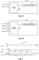
- FIG. 1A is a block diagram illustrating one example of an integrated circuit 100a to drive a plurality of fluid actuation devices.
- integrated circuit 100a is part of a fluid ejection die, which will be described below with reference to Figures 6A and 6B .
- Integrated circuit 100a includes control logic 102a, a configuration register 104, and a plurality of interfaces including a data interface 110 and a mode interface 112. Data interface 110 and mode interface 112 are electrically coupled to control logic 102.
- Control logic 102a is electrically coupled to configuration register 104.
- Control logic 102a enables writing to the configuration register 104 in response to a signal on the mode interface 112 transitioning to logic high with a logic high signal on the data interface 110.
- control logic 102a disables writing to the configuration register 104 in response to a logic low signal on the mode interface 112.
- Configuration register 104 may receive serial data from the data interface 110 with the configuration register 104 enabled for writing.
- Control logic 102a may include a microprocessor, an application-specific integrated circuit (ASIC), or other suitable logic circuitry for controlling the operation of integrated circuit 100a.
- Configuration register 104 may be a memory device (e.g., nonvolatile memory, shift register, etc.) and may include any suitable number of bits (e.g., 4 bits to 24 bits, such as 12 bits). Configuration register 104 may store configuration data for testing integrated circuit 100a, detecting cracks within a substrate of integrated circuit 100a, enabling watchdogs of integrated circuit 100a, setting analog delays of integrated circuit 100a, enabling access to memory of integrated circuit 100a, validating operations of integrated circuit 100a, or for configuring other functions of integrated circuit 100a.
- Each of the plurality of interfaces including the data interface 110 and the mode interface 112 may be a contact pad, a pin, a bump, a wire, or another suitable electrical interface for transmitting signals to control logic 102a and/or for receiving signals from control logic 102a.
- Each of the plurality of interfaces may be electrically coupled to a fluid ejection system (e.g., a printer).
- FIG. 1B is a block diagram illustrating another example of an integrated circuit 100b to drive a plurality of fluid actuation devices.
- integrated circuit 100b is part of a fluid ejection die, which will be described below with reference to Figures 6A and 6B .
- Integrated circuit 100b is similar to integrated circuit 100a previously described and illustrated with reference to Figure 1A and includes control logic 102b, a configuration register 104, and a plurality of interfaces including a data interface 110, a mode interface 112, a fire interface 114, and a clock interface 116.
- Data interface 110, mode interface 112, fire interface 114, and clock interface 116 are electrically coupled to control logic 102b.
- Control logic 102b is electrically coupled to configuration register 104.
- Control logic 102b enables writing to the configuration register 104 in response to the signal on the mode interface 110 transitioning to logic high with a logic high signal on the data interface 110 and a logic low signal on the fire interface 114. In one example, control logic 102b disables writing to the configuration register 104 in response to a logic low signal on the mode interface 112.
- Configuration register 104 may receive serial data from the data interface 110 with the configuration register 104 enabled for writing. In one example, the configuration register 104 may receive the serial data from the data interface 110 aligned with a clock signal from the clock interface 116.
- Control logic 102b may include a microprocessor, an ASIC, or other suitable logic circuitry for controlling the operation of integrated circuit 100b.
- Configuration register 104 may store configuration data for testing integrated circuit 100b, detecting cracks within a substrate of integrated circuit 100b, enabling watchdogs of integrated circuit 100b, setting analog delays of integrated circuit 100b, enabling access to memory of integrated circuit 100b, validating operations of integrated circuit 100b, or for configuring other functions of integrated circuit 100b.
- Each of the plurality of interfaces including the data interface 110, the mode interface 112, the fire interface 114, and the clock interface 116 may be a contact pad, a pin, a bump, a wire, or another suitable electrical interface for transmitting signals to control logic 102b and/or for receiving signals from control logic 102b.
- Each of the plurality of interfaces may be electrically coupled to a fluid ejection system (e.g., a printer).
- FIG. 2 is a timing diagram 200 illustrating one example for accessing a configuration register of an integrated circuit, such as configuration register 104 of integrated circuit 100b of Figure 1B .
- Timing diagram 200 includes a mode signal on a mode interface (e.g., mode interface 112), a fire signal on a fire interface (e.g., fire interface 114), a clock signal on a clock interface (e.g., clock interface 116), and a data signal on a data interface (e.g., data interface 110).
- a mode signal on a mode interface e.g., mode interface 112
- a fire signal on a fire interface e.g., fire interface 114
- a clock signal on a clock interface e.g., clock interface 116
- a data signal on a data interface e.g., data interface 110.
- the configuration register is enabled for writing in response to the mode signal transitioning from a logic low to a logic high as indicated at 206.
- a data stream provided by the data signal may be written to the configuration register.
- a four bit data stream i.e., bits B3, B2, B1, and B0
- bits B3, B2, B1, and B0 are written to the configuration register.
- any suitable number of bits may be written to the configuration register.
- Each bit of the data stream may be written to the configuration register in response to the clock signal. For example, the rising edge of the clock signal as indicated at 208 may write (e.g., latch) the B3 bit into the configuration register. Likewise, the rising edges of the clock signal as indicated at 210, 212, and 214 may write (e.g., latch) bits B2, B1, and B0, respectively, into the configuration register.
- each bit of the data stream may be written to the configuration register in response to each corresponding falling edge of the clock signal or in response to the rising and falling edges of the clock signal.
- the configuration register is a shift register
- the data stream may be written to the configuration register by shifting the data stream into the configuration register such that previous and/or extra bits are shifted out of the configuration register. Writing to the configuration register may be disabled by transitioning the mode signal back to a logic low as indicated at 216.
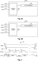
- FIG. 3A is a block diagram illustrating another example of an integrated circuit 300a to drive a plurality of fluid actuation devices.
- integrated circuit 300a is part of a fluid ejection die, which will be described below with reference to Figures 6A and 6B .
- Integrated circuit 300a includes control logic 302a, a status register 304, and a plurality of interfaces including a data interface 310, a mode interface 312, and a fire interface 314. Data interface 310, mode interface 312, and fire interface 314 are electrically coupled to control logic 302a.
- Control logic 302a is electrically coupled to status register 304.
- Control logic 302a enables reading of the status register 304 in response to both a signal on the mode interface 312 transitioning to logic high with a logic high signal on the data interface 310 and transitioning a signal on the fire interface 314 to logic high with the signal on the data interface 310 floating. In one example, control logic 302a disables reading of the status register 304 in response to a logic low signal on the mode interface 312. In another example, control logic 302a disables reading of the status register 304 in response to a logic low signal on the fire interface 314. The status register 304 may output serial data to the data interface 310 with the status register 304 enabled for reading.
- Control logic 302a may include a microprocessor, an ASIC, or other suitable logic circuitry for controlling the operation of integrated circuit 300a.
- Status register 304 may be a memory device (e.g., nonvolatile memory, shift register, etc.) and may include any suitable number of bits (e.g., 1 bit to 12 bits, such as 5 bits).
- Status register 304 may store status data such as a revision status for integrated circuit 300a, a watchdog status of integrated circuit 300a, or other suitable status data for integrated circuit 300a.
- Each of the plurality of interfaces including the data interface 310, the mode interface 312, and the fire interface 314 may be a contact pad, a pin, a bump, a wire, or another suitable electrical interface for transmitting signals to control logic 302a and/or for receiving signals from control logic 302a.
- Each of the plurality of interfaces may be electrically coupled to a fluid ejection system (e.g., a printer).
- FIG. 3B is a block diagram illustrating another example of an integrated circuit 300b to drive a plurality of fluid actuation devices.
- integrated circuit 300b is part of a fluid ejection die, which will be described below with reference to Figures 6A and 6B .
- Integrated circuit 300b is similar to integrated circuit 300a previously described and illustrated with reference to Figure 3A and includes control logic 302b, a status register 304, and a plurality of interfaces including a data interface 310, a mode interface 312, a fire interface 314, and a clock interface 316.
- Data interface 310, mode interface 312, fire interface 314, and clock interface 316 are electrically coupled to control logic 302b.
- Control logic 302b is electrically coupled to status register 304.
- Control logic 302b enables reading of the status register 304 in response to both a signal on the mode interface 312 transitioning to logic high with a logic high signal on the data interface 310 and transitioning a signal on the fire interface 314 to logic high with the signal on the data interface 310 floating.
- control logic 302b disables reading of the status register 304 in response to a logic low signal on the mode interface 312.
- control logic 302b disables reading of the status register 304 in response to a logic low signal on the fire interface 314.
- the status register 304 may output serial data to the data interface 310 with the status register 304 enabled for reading.
- the status register 304 outputs the serial data to the data interface 310 aligned with a clock signal on the clock interface 316.
- Control logic 302b may include a microprocessor, an ASIC, or other suitable logic circuitry for controlling the operation of integrated circuit 300b.
- Status register 304 may store status data such as a revision status for integrated circuit 300b, a watchdog status of integrated circuit 300b, or other suitable status data for integrated circuit 300b.
- Each of the plurality of interfaces including the data interface 310, the mode interface 312, the fire interface 314, and the clock interface 316 may be a contact pad, a pin, a bump, a wire, or another suitable electrical interface for transmitting signals to control logic 302b and/or for receiving signals from control logic 302b.
- Each of the plurality of interfaces may be electrically coupled to a fluid ejection system (e.g., a printer).
- FIG. 4 is a timing diagram 400 illustrating one example for accessing a status register of an integrated circuit, such as status register 304 of integrated circuit 300b of Figure 3B .
- Timing diagram 400 includes a mode signal on a mode interface (e.g., mode interface 312), a fire signal on a fire interface (e.g., fire interface 314), a clock signal on a clock interface (e.g., clock interface 316), and a data signal on a data interface (e.g., data interface 310).
- a logic high data signal as indicated at 402
- the mode signal is transitioned from a logic low to a logic high as indicated at 404.
- the data signal is then transitioned to floating as indicated at 406.
- the fire signal is transitioned from a logic low to a logic high as indicated at 408 to enable reading of the status register.
- the status register may output a data stream via the data signal.
- the data stream i.e., bits MSB, MSB-1, MSB-2, MSB-3, etc.
- the data stream i.e., bits MSB, MSB-1, MSB-2, MSB-3, etc.
- the data stream is read from the status register. Any suitable number of bits may be read from the status register.
- Each bit of the data stream may be read from the status register in response to the clock signal.
- the MSB bit may be read from the status register in response to enabling the status register for reading.
- the rising edge of the clock signal as indicated at 410 may output the MSB-1 bit via the data signal.
- the rising edges of the clock signal as indicated at 412, 414, etc. may output bits MSB-2, MSB-3, etc., respectively, via the data signal.
- each bit of the data stream may be output from the status register in response to each corresponding falling edge of the clock signal or in response to the rising and falling edges of the clock signal. Reading of the status register may be disabled by transitioning the fire signal back to a logic low as indicated at 416 and/or by transitioning the mode signal back to a logic low as indicated at 418.
- FIG. 5 is a block diagram illustrating another example of an integrated circuit 500 to drive a plurality of fluid actuation devices.
- integrated circuit 500 is part of a fluid ejection die, which will be described below with reference to Figures 6A and 6B .
- Integrated circuit 500 may include the features of integrated circuit 100a ( Fig. 1A ) or 100b ( Fig. 1B ) and the features of integrated circuit 300a ( Fig. 3A ) or 300b ( Fig. 3B ).
- Integrated circuit 500 includes control logic 502, a configuration register 104, a status register 304, and a plurality of interfaces including a data interface 510, a mode interface 512, a fire interface 514, and a clock interface 516.
- Data interface 510, mode interface 512, fire interface 514, and clock interface 516 are electrically coupled to control logic 502.
- Control logic 502 is electrically coupled to configuration register 104 and status register 304.
- Control logic 502 enables writing to the configuration register 104 in response to the signal on the mode interface 510 transitioning to logic high with a logic high signal on the data interface 510 and a logic low signal on the fire interface 514. In one example, control logic 502 disables writing to the configuration register 104 in response to a logic low signal on the mode interface 512.
- Configuration register 104 may receive serial data from the data interface 510 with the configuration register 104 enabled for writing. In one example, the configuration register 104 may receive the serial data from the data interface 510 aligned with a clock signal from the clock interface 516.
- control logic 502 enables reading of the status register 304 in response to both a signal on the mode interface 512 transitioning to logic high with a logic high signal on the data interface 510 and transitioning a signal on the fire interface 514 to logic high with the signal on the data interface 510 floating.
- control logic 502 disables reading of the status register 304 in response to a logic low signal on the mode interface 512.
- control logic 502 disables reading of the status register 304 in response to a logic low signal on the fire interface 514.
- the status register 304 may output serial data to the data interface 510 with the status register 304 enabled for reading.
- the status register 304 outputs the serial data to the data interface 510 aligned with a clock signal on the clock interface 516.
- Control logic 502 may include a microprocessor, an ASIC, or other suitable logic circuitry for controlling the operation of integrated circuit 500.
- the configuration register 104 and the status register 304 were previously described above with reference to Figures 1A-1B and 3A-3B , respectively.
- Each of the plurality of interfaces including the data interface 510, the mode interface 512, the fire interface 514, and the clock interface 516 may be a contact pad, a pin, a bump, a wire, or another suitable electrical interface for transmitting signals to control logic 502 and/or for receiving signals from control logic 502.
- Each of the plurality of interfaces may be electrically coupled to a fluid ejection system (e.g., a printer).
- Figure 6A illustrates one example of a fluid ejection die 600 and Figure 6B illustrates an enlarged view of the ends of fluid ejection die 600.
- Die 600 includes a first column 602 of contact pads, a second column 604 of contact pads, and a column 606 of fluid actuation devices 608.
- the second column 604 of contact pads is aligned with the first column 602 of contact pads and at a distance (i.e., along the Y axis) from the first column 602 of contact pads.
- the column 606 of fluid actuation devices 608 is disposed longitudinally to the first column 602 of contact pads and the second column 604 of contact pads.
- the column 606 of fluid actuation devices 608 is also arranged between the first column 602 of contact pads and the second column 604 of contact pads.
- fluid actuation devices 608 are nozzles or fluidic pumps to eject fluid drops.
- the first column 602 of contact pads includes six contact pads.
- the first column 602 of contact pads may include the following contact pads in order: a data contact pad 610, a clock contact pad 612, a logic power ground return contact pad 614, a multipurpose input/output contact pad 616, a first high voltage power supply contact pad 618, and a first high voltage power ground return contact pad 620. Therefore, the first column 602 of contact pads includes the data contact pad 610 at the top of the first column 602, the first high voltage power ground return contact pad 620 at the bottom of the first column 602, and the first high voltage power supply contact pad 618 directly above the first high voltage power ground return contact pad 620. While contact pads 610, 612, 614, 616, 618, and 620 are illustrated in a particular order, in other examples the contact pads may be arranged in a different order.
- the second column 604 of contact pads includes six contact pads.
- the second column 604 of contact pads may include the following contact pads in order: a second high voltage power ground return contact pad 622, a second high voltage power supply contact pad 624, a logic reset contact pad 626, a logic power supply contact pad 628, a mode contact pad 630, and a fire contact pad 632. Therefore, the second column 604 of contact pads includes the second high voltage power ground return contact pad 622 at the top of the second column 604, the second high voltage power supply contact pad 624 directly below the second high voltage power ground return contact pad 622, and the fire contact pad 632 at the bottom of the second column 604. While contact pads 622, 624, 626, 628, 630, and 632 are illustrated in a particular order, in other examples the contact pads may be arranged in a different order.
- data contact pad 610 may provide data interface 110 of Figures 1A or 1B , data interface 310 of Figures 3A or 3B , or data interface 510 of Figure 5 .
- Mode contact pad 630 may provide mode interface 112 of Figures 1A or 1B , mode interface 312 of Figures 3A or 3B , or mode interface 512 of Figure 5 .
- Fire contact pad 632 may provide fire interface 114 of Figure 1B , fire interface 314 of Figures 3A or 3B , or fire interface 514 of Figure 5 .
- Clock contact pad 612 may provide clock interface 116 of Figure 1B , clock interface 316 of Figure 3B , or clock interface 516 of Figure 5 .
- Data contact pad 610 may be used to input serial data to die 600 for selecting fluid actuation devices, memory bits, thermal sensors, configuration modes (e.g. via a configuration register 104), etc. Data contact pad 610 may also be used to output serial data from die 600 for reading memory bits, configuration modes, status information (e.g., via a status register 304), etc.
- Clock contact pad 612 may be used to input a clock signal to die 600 to shift serial data on data contact pad 610 into the die or to shift serial data out of the die to data contact pad 610.
- Logic power ground return contact pad 614 provides a ground return path for logic power (e.g., about 0 V) supplied to die 600. In one example, logic power ground return contact pad 614 is electrically coupled to the semiconductor (e.g., silicon) substrate 640 of die 600.
- Multipurpose input/output contact pad 616 may be used for analog sensing and/or digital test modes of die 600.
- First high voltage power supply contact pad 618 and second high voltage power supply contact pad 624 may be used to supply high voltage (e.g., about 32 V) to die 600.
- First high voltage power ground return contact pad 620 and second high voltage power ground return contact pad 622 may be used to provide a power ground return (e.g., about 0 V) for the high voltage power supply.
- the high voltage power ground return contact pads 620 and 622 are not directly electrically connected to the semiconductor substrate 640 of die 600.
- the specific contact pad order with the high voltage power supply contact pads 618 and 624 and the high voltage power ground return contact pads 620 and 622 as the innermost contact pads may improve power delivery to die 600. Having the high voltage power ground return contact pads 620 and 622 at the bottom of the first column 602 and at the top of the second column 604, respectively, may improve reliability for manufacturing and may improve ink shorts protection.
- Logic reset contact pad 626 may be used as a logic reset input to control the operating state of die 600.
- Logic power supply contact pad 628 may be used to supply logic power (e.g., between about 1.8 V and 15 V, such as 5.6 V) to die 600.
- Mode contact pad 630 may be used as a logic input to control access to enable/disable configuration modes (i.e., functional modes) of die 600.
- Fire contact pad 632 is used as a logic input to latch loaded data from data contact pad 610 and to enable fluid actuation devices or memory elements of die 600.
- Die 600 includes an elongate substrate 640 having a length 642 (along the Y axis), a thickness 644 (along the Z axis), and a width 646 (along the X axis).
- the length 642 is at least twenty times the width 646.
- the width 646 may be 1 mm or less and the thickness 644 may be less than 500 microns.
- the fluid actuation devices 608 e.g., fluid actuation logic
- contact pads 610-632 are provided on the elongate substrate 640 and are arranged along the length 642 of the elongate substrate. Fluid actuation devices 608 have a swath length 652 less than the length 642 of the elongate substrate 640.
- the swath length 652 is at least 1.2 cm.
- the contact pads 610-632 may be electrically coupled to the fluid actuation logic.
- the first column 602 of contact pads may be arranged near a first longitudinal end 648 of the elongate substrate 640.
- the second column 604 of contact pads may be arranged near a second longitudinal end 650 of the elongate substrate 640 opposite to the first longitudinal end 648.
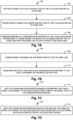
- Figures 7A-7D are flow diagrams illustrating one example of a method 700 for accessing a fluid ejection die.
- method 700 includes setting a signal on a data contact pad of the fluid ejection die to logic high.
- method 700 includes transitioning a signal on a mode contact pad of the fluid ejection die to logic high.
- method 700 includes enabling writing to a configuration register of the fluid ejection die in response to transitioning the signal on the mode contact pad to logic high with the signal on the data contact pad logic high.
- method 700 may also include transitioning the signal on the mode contact pad to logic low.
- method 700 may include disabling writing to the configuration register in response to the logic low signal on the mode contact pad.
- method 700 may also include with the configuration register enabled for writing, applying a serial data signal to the data contact pad to write the serial data to the configuration register.
- method 700 may also include with the configuration register enabled for writing, applying the serial data signal to the data contact pad aligned with a clock signal on a clock contact pad of the fluid ejection die.
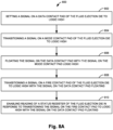
- Figures 8A-8E are flow diagrams illustrating another example of a method 800 for accessing a fluid ejection die.
- method 800 includes setting a signal on a data contact pad of the fluid ejection die to logic high.
- method 800 includes transitioning a signal on a mode contact pad of the fluid ejection die to logic high.
- method 800 includes floating the signal on the data contact pad with the signal on the mode contact pad logic high.
- method 800 includes transitioning a signal on a fire contact pad of the fluid ejection die to logic high with the signal on the data contact pad floating.
- method 800 includes enabling reading of a status register of the fluid ejection die in response to transitioning the signal on the fire contact pad to logic high with the signal on the data contact pad floating.
- method 800 may also include transitioning the signal on the mode contact pad to logic low.
- method 800 may include disabling reading of the status register in response to the logic low signal on the mode contact pad.
- method 800 may also include transitioning the signal on the fire contact pad to logic low.
- method 800 may include disabling reading of the status register in response to the logic low signal on the fire contact pad.
- method 800 may also include with the status register enabled for reading, outputting serial data from the status register to the data contact pad.
- method 800 may also include with the status register enabled for reading, outputting serial data from the status register to the data contact pad aligned with a clock signal on a clock signal pad of the fluid ejection die.
- Fluid ejection system 900 includes a fluid ejection assembly, such as printhead assembly 902, and a fluid supply assembly, such as ink supply assembly 910.
- fluid ejection system 900 also includes a service station assembly 904, a carriage assembly 916, a print media transport assembly 918, and an electronic controller 920. While the following description provides examples of systems and assemblies for fluid handling with regard to ink, the disclosed systems and assemblies are also applicable to the handling of fluids other than ink.
- Printhead assembly 902 includes at least one printhead or fluid ejection die 600 previously described and illustrated with reference to Figures 6A and 6B , which ejects drops of ink or fluid through a plurality of orifices or nozzles 608.
- the drops are directed toward a medium, such as print media 924, so as to print onto print media 924.
- print media 924 includes any type of suitable sheet material, such as paper, card stock, transparencies, Mylar, fabric, and the like.
- print media 924 includes media for three-dimensional (3D) printing, such as a powder bed, or media for bioprinting and/or drug discovery testing, such as a reservoir or container.
- nozzles 608 are arranged in at least one column or array such that properly sequenced ejection of ink from nozzles 608 causes characters, symbols, and/or other graphics or images to be printed upon print media 924 as printhead assembly 902 and print media 924 are moved relative to each other.
- Ink supply assembly 910 supplies ink to printhead assembly 902 and includes a reservoir 912 for storing ink. As such, in one example, ink flows from reservoir 912 to printhead assembly 902. In one example, printhead assembly 902 and ink supply assembly 910 are housed together in an inkjet or fluid-jet print cartridge or pen. In another example, ink supply assembly 910 is separate from printhead assembly 902 and supplies ink to printhead assembly 902 through an interface connection 913, such as a supply tube and/or valve.
- Carriage assembly 916 positions printhead assembly 902 relative to print media transport assembly 918, and print media transport assembly 918 positions print media 924 relative to printhead assembly 902.
- a print zone 926 is defined adjacent to nozzles 608 in an area between printhead assembly 902 and print media 924.
- printhead assembly 902 is a scanning type printhead assembly such that carriage assembly 916 moves printhead assembly 902 relative to print media transport assembly 918.
- printhead assembly 902 is a non-scanning type printhead assembly such that carriage assembly 916 fixes printhead assembly 902 at a prescribed position relative to print media transport assembly 918.
- Service station assembly 904 provides for spitting, wiping, capping, and/or priming of printhead assembly 902 to maintain the functionality of printhead assembly 902 and, more specifically, nozzles 608.
- service station assembly 904 may include a rubber blade or wiper which is periodically passed over printhead assembly 902 to wipe and clean nozzles 608 of excess ink.
- service station assembly 904 may include a cap that covers printhead assembly 902 to protect nozzles 608 from drying out during periods of non-use.
- service station assembly 904 may include a spittoon into which printhead assembly 902 ejects ink during spits to ensure that reservoir 912 maintains an appropriate level of pressure and fluidity, and to ensure that nozzles 608 do not clog or weep.
- Functions of service station assembly 904 may include relative motion between service station assembly 904 and printhead assembly 902.
- Electronic controller 920 communicates with printhead assembly 902 through a communication path 903, service station assembly 904 through a communication path 905, carriage assembly 916 through a communication path 917, and print media transport assembly 918 through a communication path 919.
- electronic controller 920 and printhead assembly 902 may communicate via carriage assembly 916 through a communication path 901.
- Electronic controller 920 may also communicate with ink supply assembly 910 such that, in one implementation, a new (or used) ink supply may be detected.
- Electronic controller 920 receives data 928 from a host system, such as a computer, and may include memory for temporarily storing data 928.
- Data 928 may be sent to fluid ejection system 900 along an electronic, infrared, optical or other information transfer path.
- Data 928 represent, for example, a document and/or file to be printed. As such, data 928 form a print job for fluid ejection system 900 and includes at least one print job command and/or command parameter.
- electronic controller 920 provides control of printhead assembly 902 including timing control for ejection of ink drops from nozzles 608. As such, electronic controller 920 defines a pattern of ejected ink drops which form characters, symbols, and/or other graphics or images on print media 924. Timing control and, therefore, the pattern of ejected ink drops, is determined by the print job commands and/or command parameters.
- logic and drive circuitry forming a portion of electronic controller 920 is located on printhead assembly 902. In another example, logic and drive circuitry forming a portion of electronic controller 920 is located off printhead assembly 902.
Landscapes
- Particle Formation And Scattering Control In Inkjet Printers (AREA)
- Ink Jet (AREA)
- Information Transfer Systems (AREA)
Claims (10)
- Druckkopfanordnung (902), die eine integrierte Schaltung (100a, 100b), um eine Vielzahl von Fluibetätigungsvorrichtungen anzutreiben, umfasst, wobei die integrierte Schaltung (100a, 100b) umfasst:ein Konfigurationsregister (104);eine Vielzahl von Schnittstellen, die eine Modusschnittstelle (112), eine Datenschnittstelle (110) und eine Abfeuerungsschnittstelle (114) umfassen, wobei die Abfeuerungsschnittstelle (114) dazu konfiguriert ist, als eine Logikeingabe zu fungieren, um geladene Daten von der Datenschnittstelle (110) zwischenzuspeichern und die Vielzahl von Fluidbetätigungsvorrichtungen zu aktivieren; undSteuerlogik (102a, 102b), die dazu konfiguriert ist, ein Schreiben in das Konfigurationsregister (104) als Reaktion auf ein Signal auf der Modusschnittstelle (112) zu aktivieren, das bei einem logisch hohen Signal auf der Datenschnittstelle (110) auf logisch hoch wechselt, wobei das Konfigurationsregister (104) dazu konfiguriert ist, Daten von der Datenschnittstelle (110) zu empfangen, wobei das Konfigurationsregister (104) zum Schreiben aktiviert ist, wobei die integrierte Schaltung (100a, 100b) ein Statusregister (304) umfasst, und die Steuerlogik dazu konfiguriert ist, ein Lesen des Statusregisters (304) als Reaktion sowohl auf ein Signal auf der Modusschnittstelle (112), das bei einem logisch hohen Signal auf der Datenschnittstelle (110) auf logisch hoch wechselt, als auch ein Signal auf der Abfeuerungsschnittstelle (114) auf logisch hoch wechselt, zu aktivieren, wobei das Signal auf der Datenschnittstelle (110) floatet, wobei das Statusregister (304) dazu konfiguriert ist, Daten an die Datenschnittstelle (110) auszugeben, wobei das Statusregister (304) zum Lesen aktiviert ist.
- Druckkopfanordnung (902) nach Anspruch 1, wobei die Steuerlogik (102a, 102b) dazu dient, ein Schreiben in das Konfigurationsregister (104) als Reaktion auf ein logisch niedriges Signal auf der Modusschnittstelle (112) zu deaktivieren.
- Druckkopfanordnung (902) nach Anspruch 1 oder 2, wobei die Steuerlogik (102a, 102b) dazu dient, ein Schreiben in das Konfigurationsregister (104) als Reaktion darauf, dass das Signal auf der Modusschnittstelle (112) bei einem logisch hohen Signal auf der Datenschnittstelle und einem logisch niedrigen Signal auf der Abfeuerungsschnittstelle (114) auf logisch hoch wechselt, zu aktivieren.
- Druckkopfanordnung (902) (100a, 100b) nach Anspruch 1, wobei die Vielzahl von Schnittstellen eine Taktschnittstelle (116) umfasst, und
wobei das Konfigurationsregister (104) dazu dient, die seriellen Daten von der Datenschnittstelle (110) zu empfangen, die an einem Taktsignal von der Taktschnittstelle (116) ausgerichtet sind. - Druckkopfanordnung (902) nach einem der Ansprüche 1 bis 4, wobei die integrierte Schaltung (100a, 100b) ein Fluidausstoßchip (600) ist.
- Druckkopfanordnung (902) nach Anspruch 5, wobei der Fluidausstoßchip (600) die Vielzahl von Fluidbetätigungsvorrichtungen (608) umfasst.
- Druckkopfanordnung (902) nach Anspruch 6, wobei die Vielzahl von Fluidbetätigungsvorrichtungen (608) in einer Spalte (606) angeordnet sind, der Fluidausstoßchip (600) eine erste Spalte (602) von Kontaktpads, eine zweite Spalte (604) von Kontaktpads umfasst und die Spalte (606) von Fluidbetätigungsvorrichtungen (608) zwischen der ersten Spalte (602) von Kontaktpads und der zweiten Spalte (604) von Kontaktpads angeordnet ist.
- Druckkopfanordnung (902) nach Anspruch 7, wobei der Fluidausstoßchip (600) ein längliches Substrat (640) umfasst, die erste Spalte (602) von Kontaktpads in der Nähe eines ersten Längsendes (648) des länglichen Substrats (640) angeordnet ist und die zweite Spalte (604) von Kontaktpads in der Nähe eines zweiten Längsendes (650) des länglichen Substrats (640) gegenüber dem ersten Längsende (648) angeordnet ist.
- Druckkopfanordnung (902) nach einem der Ansprüche 5 bis 8, wobei der Fluidausstoßchip (600) ein Datenkontaktpad (610) umfasst, um die Datenschnittstelle (110) bereitzustellen.
- Druckkopfanordnung (902) nach einem der Ansprüche 5 bis 9, wobei der Fluidausstoßchip (600) ein Moduskontaktpad (630) umfasst, um die Modusschnittstelle (112) bereitzustellen.
Priority Applications (1)
| Application Number | Priority Date | Filing Date | Title |
|---|---|---|---|
| EP21198421.6A EP3967497B1 (de) | 2019-02-06 | 2019-02-06 | Ein druckkopf |
Applications Claiming Priority (3)
| Application Number | Priority Date | Filing Date | Title |
|---|---|---|---|
| EP21198421.6A EP3967497B1 (de) | 2019-02-06 | 2019-02-06 | Ein druckkopf |
| PCT/US2019/016729 WO2020162890A1 (en) | 2019-02-06 | 2019-02-06 | Accessing registers of fluid ejection devices |
| EP19706141.9A EP3710262B1 (de) | 2019-02-06 | 2019-02-06 | Zugriff auf register von flüssigkeitsausstossvorrichtungen |
Related Parent Applications (2)
| Application Number | Title | Priority Date | Filing Date |
|---|---|---|---|
| EP19706141.9A Division EP3710262B1 (de) | 2019-02-06 | 2019-02-06 | Zugriff auf register von flüssigkeitsausstossvorrichtungen |
| EP19706141.9A Division-Into EP3710262B1 (de) | 2019-02-06 | 2019-02-06 | Zugriff auf register von flüssigkeitsausstossvorrichtungen |
Publications (3)
| Publication Number | Publication Date |
|---|---|
| EP3967497A1 EP3967497A1 (de) | 2022-03-16 |
| EP3967497B1 true EP3967497B1 (de) | 2024-08-21 |
| EP3967497C0 EP3967497C0 (de) | 2024-08-21 |
Family
ID=65494581
Family Applications (3)
| Application Number | Title | Priority Date | Filing Date |
|---|---|---|---|
| EP21198421.6A Active EP3967497B1 (de) | 2019-02-06 | 2019-02-06 | Ein druckkopf |
| EP21198430.7A Active EP3967498B1 (de) | 2019-02-06 | 2019-02-06 | Ein druckkopf |
| EP19706141.9A Active EP3710262B1 (de) | 2019-02-06 | 2019-02-06 | Zugriff auf register von flüssigkeitsausstossvorrichtungen |
Family Applications After (2)
| Application Number | Title | Priority Date | Filing Date |
|---|---|---|---|
| EP21198430.7A Active EP3967498B1 (de) | 2019-02-06 | 2019-02-06 | Ein druckkopf |
| EP19706141.9A Active EP3710262B1 (de) | 2019-02-06 | 2019-02-06 | Zugriff auf register von flüssigkeitsausstossvorrichtungen |
Country Status (18)
| Country | Link |
|---|---|
| US (2) | US11760085B2 (de) |
| EP (3) | EP3967497B1 (de) |
| JP (1) | JP7177945B2 (de) |
| KR (1) | KR102630329B1 (de) |
| CN (2) | CN113412195B (de) |
| AU (1) | AU2019428622B2 (de) |
| CA (1) | CA3126132C (de) |
| CL (1) | CL2021001821A1 (de) |
| CO (1) | CO2021011665A2 (de) |
| DK (1) | DK3710262T3 (de) |
| ES (2) | ES2902424T3 (de) |
| HU (1) | HUE057068T2 (de) |
| IL (1) | IL284544A (de) |
| MX (1) | MX2021009120A (de) |
| PL (2) | PL3967498T3 (de) |
| PT (1) | PT3710262T (de) |
| SG (1) | SG11202107303XA (de) |
| WO (1) | WO2020162890A1 (de) |
Families Citing this family (1)
| Publication number | Priority date | Publication date | Assignee | Title |
|---|---|---|---|---|
| KR102630329B1 (ko) | 2019-02-06 | 2024-01-29 | 휴렛-팩커드 디벨롭먼트 컴퍼니, 엘.피. | 유체 분사 장치의 레지스터에 액세스하는 기법 |
Family Cites Families (21)
| Publication number | Priority date | Publication date | Assignee | Title |
|---|---|---|---|---|
| JPH0637811A (ja) | 1992-07-20 | 1994-02-10 | Fujitsu Ltd | ディジタル信号通信回路 |
| AU1139100A (en) | 1998-10-16 | 2000-05-08 | Silverbrook Research Pty Limited | Improvements relating to inkjet printers |
| JP4395943B2 (ja) * | 1998-11-26 | 2010-01-13 | セイコーエプソン株式会社 | 印刷装置およびその情報の管理方法 |
| US6476928B1 (en) * | 1999-02-19 | 2002-11-05 | Hewlett-Packard Co. | System and method for controlling internal operations of a processor of an inkjet printhead |
| US6439697B1 (en) | 1999-07-30 | 2002-08-27 | Hewlett-Packard Company | Dynamic memory based firing cell of thermal ink jet printhead |
| US6594185B1 (en) * | 1999-10-04 | 2003-07-15 | Seiko Epson Corporation | Write-inhibit circuit, semiconductor integrated circuit using the same, ink cartridge including the semiconductor integrated circuit, and ink-jet recording apparatus |
| JP4469531B2 (ja) * | 1999-10-04 | 2010-05-26 | セイコーエプソン株式会社 | 半導体集積回路、インクカートリッジ及びインクジェット記録装置 |
| WO2002004219A1 (en) | 2000-06-30 | 2002-01-17 | Silverbrook Research Pty Ltd | Controlling the timing of printhead nozzle firing |
| JP3870030B2 (ja) * | 2001-02-28 | 2007-01-17 | キヤノン株式会社 | 割込み制御回路を有するインクジェット記録装置および記録装置の制御方法 |
| US6471320B2 (en) * | 2001-03-09 | 2002-10-29 | Hewlett-Packard Company | Data bandwidth reduction to printhead with redundant nozzles |
| JP2003341063A (ja) | 2002-05-28 | 2003-12-03 | Canon Inc | 記録装置 |
| KR100441607B1 (ko) | 2002-10-22 | 2004-07-23 | 삼성전자주식회사 | 프린터 헤드의 직렬 데이타 어드레스 전송 방법 및 장치 |
| JP2005131875A (ja) | 2003-10-29 | 2005-05-26 | Canon Inc | 記録ヘッド基板、記録ヘッド、及び記録装置 |
| US8474943B2 (en) | 2008-03-14 | 2013-07-02 | Hewlett-Packard Development Company, L.P. | Secure access to fluid cartridge memory |
| US9919517B2 (en) | 2014-01-17 | 2018-03-20 | Hewlett-Packard Development Company, L.P. | Addressing an EPROM on a printhead |
| JP6409379B2 (ja) | 2014-07-11 | 2018-10-24 | コニカミノルタ株式会社 | インクジェットヘッド及びインクジェット記録装置 |
| CN107073940B (zh) | 2014-10-29 | 2018-11-30 | 惠普发展公司,有限责任合伙企业 | 用于打印头喷射信号控制的打印头组件、方法和打印系统 |
| US10569542B2 (en) | 2016-08-16 | 2020-02-25 | Zebra Technologies Corporation | Printhead pin configurations |
| US9938136B2 (en) | 2016-08-18 | 2018-04-10 | Stmicroelectronics Asia Pacific Pte Ltd | Fluid ejection device |
| WO2018190861A1 (en) | 2017-04-14 | 2018-10-18 | Hewlett-Packard Development Company, L.P. | Fluidic die with nozzle displacement mask register |
| KR102630329B1 (ko) | 2019-02-06 | 2024-01-29 | 휴렛-팩커드 디벨롭먼트 컴퍼니, 엘.피. | 유체 분사 장치의 레지스터에 액세스하는 기법 |
-
2019
- 2019-02-06 KR KR1020217024553A patent/KR102630329B1/ko active Active
- 2019-02-06 HU HUE19706141A patent/HUE057068T2/hu unknown
- 2019-02-06 CN CN201980091440.3A patent/CN113412195B/zh active Active
- 2019-02-06 EP EP21198421.6A patent/EP3967497B1/de active Active
- 2019-02-06 SG SG11202107303XA patent/SG11202107303XA/en unknown
- 2019-02-06 ES ES19706141T patent/ES2902424T3/es active Active
- 2019-02-06 EP EP21198430.7A patent/EP3967498B1/de active Active
- 2019-02-06 WO PCT/US2019/016729 patent/WO2020162890A1/en not_active Ceased
- 2019-02-06 CA CA3126132A patent/CA3126132C/en active Active
- 2019-02-06 PL PL21198430.7T patent/PL3967498T3/pl unknown
- 2019-02-06 US US16/768,046 patent/US11760085B2/en active Active
- 2019-02-06 EP EP19706141.9A patent/EP3710262B1/de active Active
- 2019-02-06 CN CN202211151105.8A patent/CN115339241B/zh active Active
- 2019-02-06 JP JP2021544738A patent/JP7177945B2/ja active Active
- 2019-02-06 DK DK19706141.9T patent/DK3710262T3/da active
- 2019-02-06 PL PL19706141T patent/PL3710262T3/pl unknown
- 2019-02-06 PT PT197061419T patent/PT3710262T/pt unknown
- 2019-02-06 MX MX2021009120A patent/MX2021009120A/es unknown
- 2019-02-06 AU AU2019428622A patent/AU2019428622B2/en active Active
- 2019-02-06 ES ES21198430T patent/ES2990991T3/es active Active
-
2021
- 2021-07-01 IL IL284544A patent/IL284544A/en unknown
- 2021-07-08 CL CL2021001821A patent/CL2021001821A1/es unknown
- 2021-09-03 CO CONC2021/0011665A patent/CO2021011665A2/es unknown
-
2023
- 2023-07-21 US US18/225,023 patent/US12097695B2/en active Active
Also Published As
Similar Documents
| Publication | Publication Date | Title |
|---|---|---|
| EP4721989A2 (de) | Integrierte schaltungen mit personalisierungsbits | |
| US12097695B2 (en) | Accessing registers of fluid ejection devices | |
| US20240262101A1 (en) | Multiple circuits coupled to an interface | |
| EP3845386B1 (de) | Mit einer schnittstelle gekoppelte mehrfachschaltungen | |
| RU2776431C1 (ru) | Осуществление доступа к регистрам устройств выброса текучей среды | |
| NZ779194B2 (en) | Accessing registers of fluid ejection devices | |
| EP3710278B1 (de) | Integrierte schaltungen mit personalsierungsbits |
Legal Events
| Date | Code | Title | Description |
|---|---|---|---|
| PUAI | Public reference made under article 153(3) epc to a published international application that has entered the european phase |
Free format text: ORIGINAL CODE: 0009012 |
|
| STAA | Information on the status of an ep patent application or granted ep patent |
Free format text: STATUS: REQUEST FOR EXAMINATION WAS MADE |
|
| 17P | Request for examination filed |
Effective date: 20210923 |
|
| AC | Divisional application: reference to earlier application |
Ref document number: 3710262 Country of ref document: EP Kind code of ref document: P |
|
| AK | Designated contracting states |
Kind code of ref document: A1 Designated state(s): AL AT BE BG CH CY CZ DE DK EE ES FI FR GB GR HR HU IE IS IT LI LT LU LV MC MK MT NL NO PL PT RO RS SE SI SK SM TR |
|
| GRAP | Despatch of communication of intention to grant a patent |
Free format text: ORIGINAL CODE: EPIDOSNIGR1 |
|
| STAA | Information on the status of an ep patent application or granted ep patent |
Free format text: STATUS: GRANT OF PATENT IS INTENDED |
|
| INTG | Intention to grant announced |
Effective date: 20240314 |
|
| GRAS | Grant fee paid |
Free format text: ORIGINAL CODE: EPIDOSNIGR3 |
|
| GRAA | (expected) grant |
Free format text: ORIGINAL CODE: 0009210 |
|
| STAA | Information on the status of an ep patent application or granted ep patent |
Free format text: STATUS: THE PATENT HAS BEEN GRANTED |
|
| AC | Divisional application: reference to earlier application |
Ref document number: 3710262 Country of ref document: EP Kind code of ref document: P |
|
| AK | Designated contracting states |
Kind code of ref document: B1 Designated state(s): AL AT BE BG CH CY CZ DE DK EE ES FI FR GB GR HR HU IE IS IT LI LT LU LV MC MK MT NL NO PL PT RO RS SE SI SK SM TR |
|
| REG | Reference to a national code |
Ref country code: GB Ref legal event code: FG4D |
|
| REG | Reference to a national code |
Ref country code: CH Ref legal event code: EP |
|
| REG | Reference to a national code |
Ref country code: DE Ref legal event code: R096 Ref document number: 602019057710 Country of ref document: DE |
|
| REG | Reference to a national code |
Ref country code: IE Ref legal event code: FG4D |
|
| U01 | Request for unitary effect filed |
Effective date: 20240903 |
|
| U07 | Unitary effect registered |
Designated state(s): AT BE BG DE DK EE FI FR IT LT LU LV MT NL PT RO SE SI Effective date: 20240917 |
|
| PG25 | Lapsed in a contracting state [announced via postgrant information from national office to epo] |
Ref country code: NO Free format text: LAPSE BECAUSE OF FAILURE TO SUBMIT A TRANSLATION OF THE DESCRIPTION OR TO PAY THE FEE WITHIN THE PRESCRIBED TIME-LIMIT Effective date: 20241121 |
|
| PG25 | Lapsed in a contracting state [announced via postgrant information from national office to epo] |
Ref country code: PL Free format text: LAPSE BECAUSE OF FAILURE TO SUBMIT A TRANSLATION OF THE DESCRIPTION OR TO PAY THE FEE WITHIN THE PRESCRIBED TIME-LIMIT Effective date: 20240821 Ref country code: GR Free format text: LAPSE BECAUSE OF FAILURE TO SUBMIT A TRANSLATION OF THE DESCRIPTION OR TO PAY THE FEE WITHIN THE PRESCRIBED TIME-LIMIT Effective date: 20241122 |
|
| PG25 | Lapsed in a contracting state [announced via postgrant information from national office to epo] |
Ref country code: IS Free format text: LAPSE BECAUSE OF FAILURE TO SUBMIT A TRANSLATION OF THE DESCRIPTION OR TO PAY THE FEE WITHIN THE PRESCRIBED TIME-LIMIT Effective date: 20241221 |
|
| PG25 | Lapsed in a contracting state [announced via postgrant information from national office to epo] |
Ref country code: HR Free format text: LAPSE BECAUSE OF FAILURE TO SUBMIT A TRANSLATION OF THE DESCRIPTION OR TO PAY THE FEE WITHIN THE PRESCRIBED TIME-LIMIT Effective date: 20240821 |
|
| PG25 | Lapsed in a contracting state [announced via postgrant information from national office to epo] |
Ref country code: RS Free format text: LAPSE BECAUSE OF FAILURE TO SUBMIT A TRANSLATION OF THE DESCRIPTION OR TO PAY THE FEE WITHIN THE PRESCRIBED TIME-LIMIT Effective date: 20241121 Ref country code: ES Free format text: LAPSE BECAUSE OF FAILURE TO SUBMIT A TRANSLATION OF THE DESCRIPTION OR TO PAY THE FEE WITHIN THE PRESCRIBED TIME-LIMIT Effective date: 20240821 |
|
| PG25 | Lapsed in a contracting state [announced via postgrant information from national office to epo] |
Ref country code: RS Free format text: LAPSE BECAUSE OF FAILURE TO SUBMIT A TRANSLATION OF THE DESCRIPTION OR TO PAY THE FEE WITHIN THE PRESCRIBED TIME-LIMIT Effective date: 20241121 Ref country code: PL Free format text: LAPSE BECAUSE OF FAILURE TO SUBMIT A TRANSLATION OF THE DESCRIPTION OR TO PAY THE FEE WITHIN THE PRESCRIBED TIME-LIMIT Effective date: 20240821 Ref country code: NO Free format text: LAPSE BECAUSE OF FAILURE TO SUBMIT A TRANSLATION OF THE DESCRIPTION OR TO PAY THE FEE WITHIN THE PRESCRIBED TIME-LIMIT Effective date: 20241121 Ref country code: IS Free format text: LAPSE BECAUSE OF FAILURE TO SUBMIT A TRANSLATION OF THE DESCRIPTION OR TO PAY THE FEE WITHIN THE PRESCRIBED TIME-LIMIT Effective date: 20241221 Ref country code: HR Free format text: LAPSE BECAUSE OF FAILURE TO SUBMIT A TRANSLATION OF THE DESCRIPTION OR TO PAY THE FEE WITHIN THE PRESCRIBED TIME-LIMIT Effective date: 20240821 Ref country code: GR Free format text: LAPSE BECAUSE OF FAILURE TO SUBMIT A TRANSLATION OF THE DESCRIPTION OR TO PAY THE FEE WITHIN THE PRESCRIBED TIME-LIMIT Effective date: 20241122 Ref country code: ES Free format text: LAPSE BECAUSE OF FAILURE TO SUBMIT A TRANSLATION OF THE DESCRIPTION OR TO PAY THE FEE WITHIN THE PRESCRIBED TIME-LIMIT Effective date: 20240821 |
|
| U20 | Renewal fee for the european patent with unitary effect paid |
Year of fee payment: 7 Effective date: 20250121 |
|
| PG25 | Lapsed in a contracting state [announced via postgrant information from national office to epo] |
Ref country code: SM Free format text: LAPSE BECAUSE OF FAILURE TO SUBMIT A TRANSLATION OF THE DESCRIPTION OR TO PAY THE FEE WITHIN THE PRESCRIBED TIME-LIMIT Effective date: 20240821 |
|
| PG25 | Lapsed in a contracting state [announced via postgrant information from national office to epo] |
Ref country code: CZ Free format text: LAPSE BECAUSE OF FAILURE TO SUBMIT A TRANSLATION OF THE DESCRIPTION OR TO PAY THE FEE WITHIN THE PRESCRIBED TIME-LIMIT Effective date: 20240821 |
|
| PG25 | Lapsed in a contracting state [announced via postgrant information from national office to epo] |
Ref country code: SK Free format text: LAPSE BECAUSE OF FAILURE TO SUBMIT A TRANSLATION OF THE DESCRIPTION OR TO PAY THE FEE WITHIN THE PRESCRIBED TIME-LIMIT Effective date: 20240821 |
|
| PLBE | No opposition filed within time limit |
Free format text: ORIGINAL CODE: 0009261 |
|
| STAA | Information on the status of an ep patent application or granted ep patent |
Free format text: STATUS: NO OPPOSITION FILED WITHIN TIME LIMIT |
|
| 26N | No opposition filed |
Effective date: 20250522 |
|
| PG25 | Lapsed in a contracting state [announced via postgrant information from national office to epo] |
Ref country code: MC Free format text: LAPSE BECAUSE OF FAILURE TO SUBMIT A TRANSLATION OF THE DESCRIPTION OR TO PAY THE FEE WITHIN THE PRESCRIBED TIME-LIMIT Effective date: 20240821 |
|
| REG | Reference to a national code |
Ref country code: CH Ref legal event code: PL |
|
| PG25 | Lapsed in a contracting state [announced via postgrant information from national office to epo] |
Ref country code: CH Free format text: LAPSE BECAUSE OF NON-PAYMENT OF DUE FEES Effective date: 20250228 |
|
| GBPC | Gb: european patent ceased through non-payment of renewal fee |
Effective date: 20250206 |
|
| PG25 | Lapsed in a contracting state [announced via postgrant information from national office to epo] |
Ref country code: GB Free format text: LAPSE BECAUSE OF NON-PAYMENT OF DUE FEES Effective date: 20250206 |
|
| PG25 | Lapsed in a contracting state [announced via postgrant information from national office to epo] |
Ref country code: IE Free format text: LAPSE BECAUSE OF NON-PAYMENT OF DUE FEES Effective date: 20250206 |
|
| U20 | Renewal fee for the european patent with unitary effect paid |
Year of fee payment: 8 Effective date: 20260121 |