EP3972128A1 - Interface de capteur comprenant un résonateur et un amplificateur différentiel - Google Patents
Interface de capteur comprenant un résonateur et un amplificateur différentiel Download PDFInfo
- Publication number
- EP3972128A1 EP3972128A1 EP21164252.5A EP21164252A EP3972128A1 EP 3972128 A1 EP3972128 A1 EP 3972128A1 EP 21164252 A EP21164252 A EP 21164252A EP 3972128 A1 EP3972128 A1 EP 3972128A1
- Authority
- EP
- European Patent Office
- Prior art keywords
- cantilever beam
- beam bundle
- resonator
- sensor interface
- differential amplifier
- Prior art date
- Legal status (The legal status is an assumption and is not a legal conclusion. Google has not performed a legal analysis and makes no representation as to the accuracy of the status listed.)
- Granted
Links
Images




Classifications
-
- H—ELECTRICITY
- H03—ELECTRONIC CIRCUITRY
- H03H—IMPEDANCE NETWORKS, e.g. RESONANT CIRCUITS; RESONATORS
- H03H9/00—Networks comprising electromechanical or electro-acoustic elements; Electromechanical resonators
- H03H9/24—Constructional features of resonators of material which is not piezoelectric, electrostrictive, or magnetostrictive
-
- H—ELECTRICITY
- H04—ELECTRIC COMMUNICATION TECHNIQUE
- H04R—LOUDSPEAKERS, MICROPHONES, GRAMOPHONE PICK-UPS OR LIKE ACOUSTIC ELECTROMECHANICAL TRANSDUCERS; ELECTRIC HEARING AIDS; PUBLIC ADDRESS SYSTEMS
- H04R17/00—Piezoelectric transducers; Electrostrictive transducers
- H04R17/10—Resonant transducers, i.e. adapted to produce maximum output at a predetermined frequency
-
- H—ELECTRICITY
- H03—ELECTRONIC CIRCUITRY
- H03F—AMPLIFIERS
- H03F3/00—Amplifiers with only discharge tubes or only semiconductor devices as amplifying elements
- H03F3/45—Differential amplifiers
- H03F3/45071—Differential amplifiers with semiconductor devices only
- H03F3/45076—Differential amplifiers with semiconductor devices only characterised by the way of implementation of the active amplifying circuit in the differential amplifier
- H03F3/45475—Differential amplifiers with semiconductor devices only characterised by the way of implementation of the active amplifying circuit in the differential amplifier using IC blocks as the active amplifying circuit
-
- B—PERFORMING OPERATIONS; TRANSPORTING
- B81—MICROSTRUCTURAL TECHNOLOGY
- B81B—MICROSTRUCTURAL DEVICES OR SYSTEMS, e.g. MICROMECHANICAL DEVICES
- B81B7/00—Microstructural systems ; Auxiliary parts of microstructural devices or systems
- B81B7/02—Microstructural systems ; Auxiliary parts of microstructural devices or systems containing distinct electrical or optical devices of particular relevance for their function, e.g. microelectro-mechanical systems [MEMS]
-
- G—PHYSICS
- G01—MEASURING; TESTING
- G01H—MEASUREMENT OF MECHANICAL VIBRATIONS OR ULTRASONIC, SONIC OR INFRASONIC WAVES
- G01H11/00—Measuring mechanical vibrations or ultrasonic, sonic or infrasonic waves by detecting changes in electric or magnetic properties
- G01H11/06—Measuring mechanical vibrations or ultrasonic, sonic or infrasonic waves by detecting changes in electric or magnetic properties by electric means
- G01H11/08—Measuring mechanical vibrations or ultrasonic, sonic or infrasonic waves by detecting changes in electric or magnetic properties by electric means using piezoelectric devices
-
- G—PHYSICS
- G01—MEASURING; TESTING
- G01H—MEASUREMENT OF MECHANICAL VIBRATIONS OR ULTRASONIC, SONIC OR INFRASONIC WAVES
- G01H13/00—Measuring resonant frequency
-
- H—ELECTRICITY
- H03—ELECTRONIC CIRCUITRY
- H03F—AMPLIFIERS
- H03F1/00—Details of amplifiers with only discharge tubes, only semiconductor devices or only unspecified devices as amplifying elements
- H03F1/08—Modifications of amplifiers to reduce detrimental influences of internal impedances of amplifying elements
- H03F1/083—Modifications of amplifiers to reduce detrimental influences of internal impedances of amplifying elements in transistor amplifiers
-
- H—ELECTRICITY
- H03—ELECTRONIC CIRCUITRY
- H03F—AMPLIFIERS
- H03F3/00—Amplifiers with only discharge tubes or only semiconductor devices as amplifying elements
- H03F3/181—Low-frequency amplifiers, e.g. audio preamplifiers
- H03F3/183—Low-frequency amplifiers, e.g. audio preamplifiers with semiconductor devices only
-
- H—ELECTRICITY
- H03—ELECTRONIC CIRCUITRY
- H03F—AMPLIFIERS
- H03F3/00—Amplifiers with only discharge tubes or only semiconductor devices as amplifying elements
- H03F3/45—Differential amplifiers
-
- H—ELECTRICITY
- H04—ELECTRIC COMMUNICATION TECHNIQUE
- H04R—LOUDSPEAKERS, MICROPHONES, GRAMOPHONE PICK-UPS OR LIKE ACOUSTIC ELECTROMECHANICAL TRANSDUCERS; ELECTRIC HEARING AIDS; PUBLIC ADDRESS SYSTEMS
- H04R17/00—Piezoelectric transducers; Electrostrictive transducers
- H04R17/02—Microphones
-
- H—ELECTRICITY
- H10—SEMICONDUCTOR DEVICES; ELECTRIC SOLID-STATE DEVICES NOT OTHERWISE PROVIDED FOR
- H10N—ELECTRIC SOLID-STATE DEVICES NOT OTHERWISE PROVIDED FOR
- H10N30/00—Piezoelectric or electrostrictive devices
- H10N30/30—Piezoelectric or electrostrictive devices with mechanical input and electrical output, e.g. functioning as generators or sensors
- H10N30/304—Beam type
- H10N30/306—Cantilevers
-
- H—ELECTRICITY
- H10—SEMICONDUCTOR DEVICES; ELECTRIC SOLID-STATE DEVICES NOT OTHERWISE PROVIDED FOR
- H10N—ELECTRIC SOLID-STATE DEVICES NOT OTHERWISE PROVIDED FOR
- H10N39/00—Integrated devices, or assemblies of multiple devices, comprising at least one piezoelectric, electrostrictive or magnetostrictive element covered by groups H10N30/00 – H10N35/00
-
- B—PERFORMING OPERATIONS; TRANSPORTING
- B81—MICROSTRUCTURAL TECHNOLOGY
- B81B—MICROSTRUCTURAL DEVICES OR SYSTEMS, e.g. MICROMECHANICAL DEVICES
- B81B2201/00—Specific applications of microelectromechanical systems
- B81B2201/02—Sensors
-
- B—PERFORMING OPERATIONS; TRANSPORTING
- B81—MICROSTRUCTURAL TECHNOLOGY
- B81B—MICROSTRUCTURAL DEVICES OR SYSTEMS, e.g. MICROMECHANICAL DEVICES
- B81B2203/00—Basic microelectromechanical structures
- B81B2203/01—Suspended structures, i.e. structures allowing a movement
- B81B2203/0118—Cantilevers
-
- G—PHYSICS
- G01—MEASURING; TESTING
- G01H—MEASUREMENT OF MECHANICAL VIBRATIONS OR ULTRASONIC, SONIC OR INFRASONIC WAVES
- G01H1/00—Measuring characteristics of vibrations in solids by using direct conduction to the detector
-
- H—ELECTRICITY
- H03—ELECTRONIC CIRCUITRY
- H03F—AMPLIFIERS
- H03F2200/00—Indexing scheme relating to amplifiers
- H03F2200/03—Indexing scheme relating to amplifiers the amplifier being designed for audio applications
-
- H—ELECTRICITY
- H03—ELECTRONIC CIRCUITRY
- H03F—AMPLIFIERS
- H03F2200/00—Indexing scheme relating to amplifiers
- H03F2200/126—A diode being coupled in a feedback path of an amplifier stage, e.g. active or passive diode
-
- H—ELECTRICITY
- H03—ELECTRONIC CIRCUITRY
- H03F—AMPLIFIERS
- H03F2200/00—Indexing scheme relating to amplifiers
- H03F2200/135—Indexing scheme relating to amplifiers there being a feedback over one or more internal stages in the global amplifier
-
- H—ELECTRICITY
- H03—ELECTRONIC CIRCUITRY
- H03F—AMPLIFIERS
- H03F2200/00—Indexing scheme relating to amplifiers
- H03F2200/144—Indexing scheme relating to amplifiers the feedback circuit of the amplifier stage comprising a passive resistor and passive capacitor
-
- H—ELECTRICITY
- H03—ELECTRONIC CIRCUITRY
- H03F—AMPLIFIERS
- H03F2200/00—Indexing scheme relating to amplifiers
- H03F2200/321—Use of a microprocessor in an amplifier circuit or its control circuit
-
- H—ELECTRICITY
- H03—ELECTRONIC CIRCUITRY
- H03F—AMPLIFIERS
- H03F2200/00—Indexing scheme relating to amplifiers
- H03F2200/54—Two or more capacitor coupled amplifier stages in cascade
-
- H—ELECTRICITY
- H03—ELECTRONIC CIRCUITRY
- H03F—AMPLIFIERS
- H03F2203/00—Indexing scheme relating to amplifiers with only discharge tubes or only semiconductor devices as amplifying elements covered by H03F3/00
- H03F2203/45—Indexing scheme relating to differential amplifiers
- H03F2203/45134—Indexing scheme relating to differential amplifiers the whole differential amplifier together with other coupled stages being fully differential realised
-
- H—ELECTRICITY
- H03—ELECTRONIC CIRCUITRY
- H03F—AMPLIFIERS
- H03F2203/00—Indexing scheme relating to amplifiers with only discharge tubes or only semiconductor devices as amplifying elements covered by H03F3/00
- H03F2203/45—Indexing scheme relating to differential amplifiers
- H03F2203/45138—Two or more differential amplifiers in IC-block form are combined, e.g. measuring amplifiers
-
- H—ELECTRICITY
- H03—ELECTRONIC CIRCUITRY
- H03F—AMPLIFIERS
- H03F2203/00—Indexing scheme relating to amplifiers with only discharge tubes or only semiconductor devices as amplifying elements covered by H03F3/00
- H03F2203/45—Indexing scheme relating to differential amplifiers
- H03F2203/45512—Indexing scheme relating to differential amplifiers the FBC comprising one or more capacitors, not being switched capacitors, and being coupled between the LC and the IC
-
- H—ELECTRICITY
- H03—ELECTRONIC CIRCUITRY
- H03F—AMPLIFIERS
- H03F2203/00—Indexing scheme relating to amplifiers with only discharge tubes or only semiconductor devices as amplifying elements covered by H03F3/00
- H03F2203/45—Indexing scheme relating to differential amplifiers
- H03F2203/45518—Indexing scheme relating to differential amplifiers the FBC comprising one or more diodes and being coupled between the LC and the IC
-
- H—ELECTRICITY
- H03—ELECTRONIC CIRCUITRY
- H03F—AMPLIFIERS
- H03F2203/00—Indexing scheme relating to amplifiers with only discharge tubes or only semiconductor devices as amplifying elements covered by H03F3/00
- H03F2203/45—Indexing scheme relating to differential amplifiers
- H03F2203/45526—Indexing scheme relating to differential amplifiers the FBC comprising a resistor-capacitor combination and being coupled between the LC and the IC
-
- H—ELECTRICITY
- H03—ELECTRONIC CIRCUITRY
- H03F—AMPLIFIERS
- H03F2203/00—Indexing scheme relating to amplifiers with only discharge tubes or only semiconductor devices as amplifying elements covered by H03F3/00
- H03F2203/45—Indexing scheme relating to differential amplifiers
- H03F2203/45528—Indexing scheme relating to differential amplifiers the FBC comprising one or more passive resistors and being coupled between the LC and the IC
-
- H—ELECTRICITY
- H03—ELECTRONIC CIRCUITRY
- H03F—AMPLIFIERS
- H03F2203/00—Indexing scheme relating to amplifiers with only discharge tubes or only semiconductor devices as amplifying elements covered by H03F3/00
- H03F2203/45—Indexing scheme relating to differential amplifiers
- H03F2203/45544—Indexing scheme relating to differential amplifiers the IC comprising one or more capacitors, e.g. coupling capacitors
-
- H—ELECTRICITY
- H03—ELECTRONIC CIRCUITRY
- H03F—AMPLIFIERS
- H03F2203/00—Indexing scheme relating to amplifiers with only discharge tubes or only semiconductor devices as amplifying elements covered by H03F3/00
- H03F2203/45—Indexing scheme relating to differential amplifiers
- H03F2203/45546—Indexing scheme relating to differential amplifiers the IC comprising one or more capacitors feedback coupled to the IC
-
- H—ELECTRICITY
- H03—ELECTRONIC CIRCUITRY
- H03F—AMPLIFIERS
- H03F2203/00—Indexing scheme relating to amplifiers with only discharge tubes or only semiconductor devices as amplifying elements covered by H03F3/00
- H03F2203/45—Indexing scheme relating to differential amplifiers
- H03F2203/45566—Indexing scheme relating to differential amplifiers the IC comprising one or more dif stages in cascade with the dif amp
-
- H—ELECTRICITY
- H03—ELECTRONIC CIRCUITRY
- H03F—AMPLIFIERS
- H03F2203/00—Indexing scheme relating to amplifiers with only discharge tubes or only semiconductor devices as amplifying elements covered by H03F3/00
- H03F2203/45—Indexing scheme relating to differential amplifiers
- H03F2203/45594—Indexing scheme relating to differential amplifiers the IC comprising one or more resistors, which are not biasing resistor
-
- H—ELECTRICITY
- H03—ELECTRONIC CIRCUITRY
- H03F—AMPLIFIERS
- H03F2203/00—Indexing scheme relating to amplifiers with only discharge tubes or only semiconductor devices as amplifying elements covered by H03F3/00
- H03F2203/45—Indexing scheme relating to differential amplifiers
- H03F2203/45601—Indexing scheme relating to differential amplifiers the IC comprising one or more passive resistors by feedback
-
- H—ELECTRICITY
- H03—ELECTRONIC CIRCUITRY
- H03H—IMPEDANCE NETWORKS, e.g. RESONANT CIRCUITS; RESONATORS
- H03H9/00—Networks comprising electromechanical or electro-acoustic elements; Electromechanical resonators
- H03H9/02—Details
- H03H9/02244—Details of microelectro-mechanical resonators
-
- H—ELECTRICITY
- H03—ELECTRONIC CIRCUITRY
- H03H—IMPEDANCE NETWORKS, e.g. RESONANT CIRCUITS; RESONATORS
- H03H9/00—Networks comprising electromechanical or electro-acoustic elements; Electromechanical resonators
- H03H9/02—Details
- H03H9/02244—Details of microelectro-mechanical resonators
- H03H9/02259—Driving or detection means
-
- H—ELECTRICITY
- H03—ELECTRONIC CIRCUITRY
- H03H—IMPEDANCE NETWORKS, e.g. RESONANT CIRCUITS; RESONATORS
- H03H9/00—Networks comprising electromechanical or electro-acoustic elements; Electromechanical resonators
- H03H9/15—Constructional features of resonators consisting of piezoelectric or electrostrictive material
- H03H9/17—Constructional features of resonators consisting of piezoelectric or electrostrictive material having a single resonator
-
- H—ELECTRICITY
- H03—ELECTRONIC CIRCUITRY
- H03H—IMPEDANCE NETWORKS, e.g. RESONANT CIRCUITS; RESONATORS
- H03H9/00—Networks comprising electromechanical or electro-acoustic elements; Electromechanical resonators
- H03H9/24—Constructional features of resonators of material which is not piezoelectric, electrostrictive, or magnetostrictive
- H03H9/2405—Constructional features of resonators of material which is not piezoelectric, electrostrictive, or magnetostrictive of microelectro-mechanical resonators
-
- H—ELECTRICITY
- H04—ELECTRIC COMMUNICATION TECHNIQUE
- H04R—LOUDSPEAKERS, MICROPHONES, GRAMOPHONE PICK-UPS OR LIKE ACOUSTIC ELECTROMECHANICAL TRANSDUCERS; ELECTRIC HEARING AIDS; PUBLIC ADDRESS SYSTEMS
- H04R2201/00—Details of transducers, loudspeakers or microphones covered by H04R1/00 but not provided for in any of its subgroups
- H04R2201/003—Mems transducers or their use
-
- H—ELECTRICITY
- H04—ELECTRIC COMMUNICATION TECHNIQUE
- H04R—LOUDSPEAKERS, MICROPHONES, GRAMOPHONE PICK-UPS OR LIKE ACOUSTIC ELECTROMECHANICAL TRANSDUCERS; ELECTRIC HEARING AIDS; PUBLIC ADDRESS SYSTEMS
- H04R2410/00—Microphones
- H04R2410/03—Reduction of intrinsic noise in microphones
Definitions
- Example embodiments of the present disclosure relate to sensor interfaces including resonators and differential amplifiers.
- Sound sensors may be classified into omni-directional sound sensors and directional sound sensors.
- An omni-directional sound sensor may include a filter including a membrane.
- the filter including the membrane generates an electrical signal by causing the membrane to change its capacitance according to a change in a negative pressure applied thereto.
- a directional sound sensor is capable of detecting the direction of a sound signal, and may include a filter including resonators having different resonance frequencies.
- the filter including a plurality of resonators an electric signal is generated by a resonator that resonates in response to a sound signal of a specific frequency.
- a high signal-to-noise ratio (SNR) may be considered as a design goal in relation to the filter including the plurality of resonators.
- One or more example embodiments provide sensor interfaces including resonators and differential amplifiers.
- a sensor interface including a first cantilever beam bundle including at least one resonator and a first output terminal, a second cantilever beam bundle including at least one resonator and a second output terminal, and a differential amplifier including a first input terminal electrically connected to the first output terminal of the first cantilever beam bundle and a second input terminal electrically connected to the second output terminal of the second cantilever beam bundle.
- Embodiments may relate to an interface connection structure of a microelectromechanical system (MEMS) and a pre-amplifier (pre-amp) connected thereto.
- MEMS microelectromechanical system
- pre-amp pre-amplifier
- Such a structure may be mounted on a variety of mobile devices, including microphones, sensor devices, mobile phones, vehicle assist devices, TVs, and loT smart devices that use the MEMS as a sensor.
- Proposed embodiments are therefore highly applicable to microphones and sensor devices that require a high signal-to-noise ratio (SNR) and low-cost interface circuit.
- SNR signal-to-noise ratio
- the interface connection structure may be used as an application field of sensor read-out solution within the project.
- a general structure may amplify a voice signal generated through a piezoelectric MEMS device with a pre-amplifier to be insensitive to an electrical signal of the sensor itself, which is vulnerable to noise.
- Embodiments may have the effect of reducing the chip size, price, and design burden by lowering the noise requirement of the pre-amplifier.
- Embodiments may be used as a replacement device for the microphones of the electronic devices (such as TVs and AI speakers), and may applied to electric fields and mobile devices.
- the electronic devices such as TVs and AI speakers
- embodiments may reduce the circuit noise to alleviate the design burden of the pre-amplifier, and to provide the effect of lowering the manufacturing cost and chip area.
- the beam groups connected to each other may be divided into 2 groups, so as to divide the number of inactive beams connected to the pre-amplifier input by half.
- an interface circuit connected to two inputs of an amplification unit and a pre-amplifier, comprising a plurality of first MEMS element group in which MEMS elements in a form of a cantilever beam are connected in a plurality of groups and a plurality of cantilever beam groups.
- the pre-amp amplifier may be a 2-input/differential amplifier with two inputs.
- a connection between the MEMS element groups and the amplification unit may be a resistive or capacitive coupling.
- a feedback connection in the amplification unit may be composed of only a resistor and a capacitor, or any one of them.
- a feedback connection in the amplification unit may be composed of only a diode and a capacitor.
- a feedback connection in the amplification unit may composed of only a resistor and a diode.
- the MEMS element group may be bundled with cantilever beams of the same length.
- an interface circuit connected to two inputs of an amplification unit and a pre-amplifier, comprising a plurality of first MEMS element group in which MEMS elements in a form of a cantilever beam are connected in a plurality of groups and a plurality of cantilever beam groups, wherein an upper electrode and a lower electrode of the first MEMS element group and the second MEMS element group are alternately connected to the amplification unit.
- a resonance frequency of the at least one resonator of the first cantilever beam bundle may be different from a resonance frequency of the at least one resonator of the second cantilever beam bundle.
- a frequency band of a signal filtered by the first cantilever beam bundle may be different from a frequency band of a signal filtered by the second cantilever beam bundle.
- Each of the at least one resonator of the first cantilever beam bundle and each of the at least one resonator of the second cantilever beam bundle may include a sensor device configured to generate an electrical signal based on the respective resonator vibrating.
- the sensor device may include an upper electrode, a piezoelectric material layer, and a lower electrode.
- the upper electrode of the at least one resonator of the first cantilever beam bundle may be electrically connected to the first input terminal of the differential amplifier, and the upper electrode of the at least one resonator of the second cantilever beam bundle may be electrically connected to the second input terminal of the differential amplifier.
- the upper electrode of the at least one resonator of the first cantilever beam bundle may be electrically connected to the first input terminal of the differential amplifier, and the lower electrode of the at least one resonator of the second cantilever beam bundle may be electrically connected to the second input terminal of the differential amplifier.
- the upper electrode, the piezoelectric material layer, and the lower electrode may have a same length.
- a length of one of the upper electrode, the piezoelectric material layer, and the lower electrode may be different from lengths of remaining ones of the upper electrode, the piezoelectric material layer, and the lower electrode.
- Each of the at least one resonator of the first cantilever beam bundle and each of the at least one resonator of the second cantilever beam bundle may include a support member configured to vibrate based on sound, and the lower electrode may be disposed on the support member.
- a length of the support member of the at least one resonator of the first cantilever beam bundle and a length of the support member of the at least one resonator of the second cantilever beam bundle may be same.
- the support member may be a cantilever.
- Each of the at least one resonator of the first cantilever beam bundle and each of the at least one resonator of the second cantilever beam bundle may include a fixing member configured to fix one end of the support member.
- a length of the fixing member of the at least one resonator of the first cantilever beam bundle and a length of the fixing member of the at least one resonator of the second cantilever beam bundle may be different from each other.
- the differential amplifier may include a first output terminal and a second output terminal.
- the differential amplifier may include at least one circuit element electrically connected to the first input terminal and the first output terminal, and the first input terminal may be a positive input terminal and the first output terminal may be a negative output terminal, or the first input terminal may be a negative input terminal and the first output terminal may be a positive output terminal.
- the at least one circuit element may be one of a resistor, a capacitor, and a diode.
- the sensor interface may further include at least one circuit element electrically connected to the first output terminal of the first cantilever beam bundle and the first input terminal of the differential amplifier.
- the first cantilever beam bundle may include a plurality of resonators, wherein each of the plurality of resonators include a support member, and wherein the support members of the plurality of resonators have same length and are configured to vibrate based on sound.
- a sound processing device including a sensor interface, the sensor interface including a first cantilever beam bundle including at least one resonator and a first output terminal, a second cantilever beam bundle including at least one resonator and a second output terminal, and a differential amplifier including a first input terminal electrically connected to the first output terminal of the first cantilever beam bundle and a second input terminal electrically connected to the second output terminal of the second cantilever beam bundle, and a processor configured to process an output signal of the sensor interface.
- a sensor interface including a first cantilever beam bundle including a plurality of resonators and a first output terminal, a second cantilever beam bundle including a plurality of resonators and a second output terminal, and a differential amplifier including a first input terminal electrically connected to the first output terminal of the first cantilever beam bundle and a second input terminal electrically connected to the second output terminal of the second cantilever beam bundle.
- a first frequency band of a signal filtered by the first cantilever beam bundle may be different from a second frequency band of a signal filtered by the second cantilever beam bundle.
- the expression, "at least one of a, b, and c,” should be understood as including only a, only b, only c, both a and b, both a and c, both b and c, or all of a, b, and c.
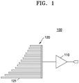
- FIG. 1 is a diagram illustrating a sensor interface 100 according to an example embodiment.
- the sensor interface 100 includes a differential amplifier 110 and a cantilever beam bundle 120.
- the cantilever beam bundle 120 may be configured to filter signals in an audible frequency band.
- the cantilever beam bundle 120 may be configured to filter a sound signal in an audible frequency band in the range of about 20 Hz to about 20 kHz.
- the cantilever beam bundle 120 may include a plurality of resonators 121. Resonance frequencies of the plurality of resonators 121 may be different. A sound signal corresponding to a resonance frequency of a resonator may be filtered by the resonator.
- the cantilever beam bundle 120 generates an electric signal by the resonator that vibrates in response to the sound signal.
- the differential amplifier 110 amplifies the electric signal to generate an output signal.
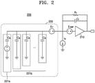
- FIG. 2 is a circuit diagram illustrating the sensor interface 200 of FIG. 1 according to an example embodiment.
- the sensor interface 200 may be interpreted as a circuit diagram of FIG. 2 , and noise of an output signal of the sensor interface 200 may be expressed as Equation 1 below.
- the noise of the output signal of the sensor interface 200 may be noise of an output signal of the differential amplifier 210.
- V noise 2 V F noise 2 + V current noise 2 + V circuit noise 2
- V current noise ⁇ I N ⁇ R f V circuit noise ⁇ E AMP ⁇ N ⁇ C B C f
- the signal-to-noise ratio (SNR) of the sensor interface 200 may be expressed as Equation 2.
- V noise denotes the noise of the output signal of the sensor interface 200
- V F noise denotes noise due to the cantilever beam bundle 220
- V current noise denotes noise due to the leakage current of the differential amplifier 210
- V circuit noise denotes noise due to the differential amplifier 210
- N denotes the number of resonators of the cantilever beam bundle 220
- C B denotes the capacitance of a resonator
- E F denotes a potential difference between an output terminal of the cantilever beam bundle 220 and ground
- E AMP denotes a potential difference between an input terminal of the differential amplifier 210 and ground
- I N denotes a leakage current of the input terminal of the differential amplifier 210
- Cf denotes a feedback capacitance of the differential amplifier 210
- Rf denotes a feedback resistance of the differential amplifier 210.
- Resonators in the cantilever beam bundle 220 are configured to have different resonance frequencies. Accordingly, when a sound signal of a specific frequency is generated, an electric signal is generated by active resonators 221a having a resonance frequency corresponding to the specific frequency.
- V F noise and V circuit noise are proportional to the number N of the resonators.
- SNR is inversely proportional to the number N of the resonators. Therefore, when the sound signal of the specific frequency is generated, noise may be generated in the sensor interface 200 due to inactive resonators 221b that do not have a resonance frequency corresponding to the specific frequency.
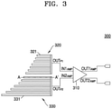
- FIG. 3 is a diagram illustrating a sensor interface 300 according to an example embodiment.
- the sensor interface 300 includes a first cantilever beam bundle 320, a second cantilever beam bundle 330, and a differential amplifier 310.
- the first cantilever beam bundle 320 and the second cantilever beam bundle 330 may be configured to filter signals in an audible frequency band.
- a frequency band of the signal filtered by the first cantilever beam bundle 320 may be different from a frequency band of the signal filtered by the second cantilever beam bundle 330.
- the first cantilever beam bundle 320 may be configured to filter the signal in the frequency band in the range of 20 Hz or more and less than 200 Hz
- the second cantilever beam bundle 330 may be configured to filter the signal in the frequency band in the range of 200 Hz or more and 20 kHz or less.
- the first cantilever beam bundle 320 may be configured to include at least one resonator 321.
- the second cantilever beam bundle 330 may be configured to include at least one resonator 331. According to design conditions, each of the first cantilever beam bundle 320 and the second cantilever beam bundle 330 may be configured to include tens to thousands of resonators.
- first cantilever beam bundle 320 and the second cantilever beam bundle 330 are configured to include the same number of resonators. In another example embodiment, the first cantilever beam bundle 320 and the second cantilever beam bundle 330 may be configured to include different numbers of resonators.
- the resonance frequency of the resonator 321 of the first cantilever beam bundle 320 may be different from the resonance frequency of the resonator 331 of the second cantilever beam bundle 330.
- resonance frequencies of the plurality of resonators may be different from each other.
- resonance frequencies of the plurality of resonators may be different from each other.
- an embodiment in which a plurality of resonators having the same resonance frequency are used is not excluded.
- the differential amplifier 310 may be configured to generate an output signal by amplifying a difference between the signal filtered by the first cantilever beam bundle 320 and the signal filtered by the second cantilever beam bundle 330.
- a first input terminal IN1 AMP of the differential amplifier 310 is electrically connected to an output terminal OUT F1 of the first cantilever beam bundle 320, and a second input terminal IN2 AMP of the differential amplifier 310 is electrically connected to an output terminal OUT F2 of the second cantilever beam bundle 330.
- the first input terminal IN1 AMP and the output terminal OUT F1 may be directly connected or indirectly connected through at least one circuit element.
- circuit elements such as a resistor, a transistor, a capacitor, or a switch may be disposed between the first input terminal IN1 AMP and the output terminal OUT F1 .
- the second input terminal IN2 AMP and the output terminal OUT F2 may also be directly connected or indirectly connected through a circuit element.
- the differential amplifier 310 includes a first output terminal OUT1 AMP and a second output terminal OUT2 AMP . In another example embodiment, the differential amplifier 310 may be configured to include one output terminal.
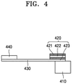
- FIG. 4 is a diagram illustrating a resonator according to an example embodiment.
- FIG. 4 is a cross-sectional view of the resonator taken along a cutting line A-A' of FIG. 3 .
- the resonator includes a fixing member 410, a sensor unit 420, a support member 430, and a mass body 440.
- the fixing member 410 is configured to fix one end of the support member 430.
- the support member 430 may be a beam.
- the support member 430 is a cantilever, and the mass body 440 is disposed at the other end of the support member 430.
- the support member 430 may include silicon (Si) or the like, but is not limited thereto.
- the mass body 440 may include a metal such as gold (Au), but is not limited thereto.
- the sensor unit 420 which is a sensor device is disposed at one end of the support member 430.
- the sensor unit 420 may generate an electric signal as the resonator vibrates.
- the sensor unit 420 may be a piezo sensor.
- the sensor unit 420 may include an upper electrode 421, a lower electrode 423, and a piezoelectric material layer 422 disposed between the upper electrode 421 and the lower electrode 423.
- the lower electrode 423 may be disposed on the support member 430.
- the lower electrode 423 may be disposed directly on the support member 430.
- the lower electrode 423 may be disposed above the support member 430.
- an insulating layer may be selectively disposed between the lower electrode 423 and the support member 430.
- the upper electrode 421 and the lower electrode 423 may include a metal material such as molybdenum (Mo).
- the piezoelectric material layer 422 may include aluminum nitride (AIN), zinc oxide (ZnO), tin (II) oxide (SnO), lead titanium zirconium oxide (PZT), tin zinc oxide (ZnSnO3), polyvinylidene fluoride (PVDF), poly(vinylidene fluoride-trifluoroethylene) (P(VDF-TrFE)), or PMN-PT, but is not limited thereto.
- the upper electrode 421, the piezoelectric material layer 422, and the lower electrode 423 may be configured to have the same length, width, and area. Alternatively, length, width, or thickness of any one of the upper electrode 421, the piezoelectric material layer 422, and the lower electrode 423 may be configured to be different from the corresponding lengths, widths, or thicknesses of the other ones.
- Each of resonators may be configured to have a separate upper electrode 421, a piezoelectric material layer 422, and a lower electrode 423.
- each of the resonators may be configured to include the upper electrode 421 and the piezoelectric material layer 422, and all of the resonators may be configured to include the lower electrode 423 as a common electrode.
- each of the resonators may be configured to include the lower electrode 423 and the piezoelectric material layer 422, and all of the resonators may be configured to include the upper electrode 421 as a common electrode.
- an inertial force may be generated according to the movement of the mass body 440.
- the resonance frequency of the support member 430 coincides with the frequency of external vibration, sound, or force
- a resonance phenomenon occurs and inertia force increases.
- the increased inertia force generates a bending moment in the sensor unit 420, and the bending moment induces stress in each layer of the sensor unit 420.
- the piezoelectric material layer 422 may generate charge having the magnitude proportional to the stress applied to the piezoelectric material layer 422, and generates voltage inversely proportional to the capacitance between the upper electrode 421 and the lower electrode 423.
- the voltage generated in the sensor unit 420 may be detected and analyzed by an external force such as vibration, sound, or force from the outside, and thus information about the external force may be obtained
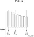
- FIG. 5 is a diagram illustrating a relationship between lengths of resonators and resonance frequencies according to an example embodiment.
- a sensor interface according to an example embodiment may include resonators having different resonance frequencies.
- the resonance frequencies of the resonators may be different from each other. In this case, the shorter the length of the support member, the higher the resonance frequency of the resonator may be.
- the resonance frequencies of the resonators may be different from each other.
- the length of a fixing member increases in a direction parallel to the support member, a fixed part in the support member increases, and thus the length of a non-fixed part in the support member may be reduced. Therefore, in this case, as the length of the fixing member increases, the resonance frequency of the resonator may increase.
- lengths of support members of first and second cantilever beam bundles may be the same, and lengths of fixing members may be different.
- the resonators included in one cantilever beam bundle may be configured to include support members of the same length and fixing members of different lengths.
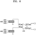
- FIG. 6 is a diagram illustrating a connection method of resonators and a differential amplifier 610 according to an example embodiment.
- FIG. 6 illustrates a sensor unit 620 of the resonator of a first cantilever beam bundle, a sensor unit 630 of the resonator of a second cantilever beam bundle, and the differential amplifier 610 according to an example embodiment.
- the sensor unit 620 includes an upper electrode 621, a piezoelectric material layer 622, and a lower electrode 623
- the sensor unit 630 includes an upper electrode 631 and a piezoelectric material layer 632, and a lower electrode 633.
- Lengths, widths, or thicknesses of the sensor unit 620 and the sensor unit 630 may be the same or different.
- length, width, or thickness of each of the upper electrode 621, the piezoelectric material layer 622, and the lower electrode 623 may be the same as or different from length, width, or thickness of each of the corresponding upper electrode 631, piezoelectric material layer 632, and lower electrode 633.
- a first input terminal IN1 AMP of the differential amplifier 610 is electrically connected to the upper electrode 621 of the sensor unit 620, and a second input terminal IN2 AMP of the differential amplifier 610 is electrically connected to the upper electrode 631 of the sensor unit 630.
- the lower electrode 623 of the sensor unit 620 and the lower electrode 633 of the sensor unit 630 may be grounded.
- Lower electrodes of the sensor units 620 of the resonators of the first cantilever beam bundle may be separately grounded through a plurality of terminals or grounded through one terminal.
- lower electrodes of the sensor units 630 of the resonators of the second cantilever beam bundle may be separately grounded through a plurality of terminals or grounded through one terminal.
- an output signal V out of the differential amplifier 610 may be expressed as Equation 3.
- V out G V 1 ⁇ V 2
- Equation 3 G denotes a gain of the differential amplifier 610.
- An n-th resonance frequency of the resonator of the first cantilever beam bundle and an m-th resonance frequency of the resonator of the second cantilever beam bundle may be the same of may be different.
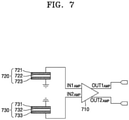
- FIG. 7 is a diagram illustrating a connection method of resonators and a differential amplifier 710 according to an example embodiment.
- FIG. 7 illustrates a sensor unit 720 of the resonator of a first cantilever beam bundle, a sensor unit 730 of the resonator of a second cantilever beam bundle, and the differential amplifier 710 according to an example embodiment.
- the sensor unit 720 includes an upper electrode 721, a piezoelectric material layer 722, and a lower electrode 723, and the sensor unit 730 includes an upper electrode 731 and a piezoelectric material layer 732, and a lower electrode 733.
- the first input terminal IN1 AMP of the differential amplifier 710 is electrically connected to the upper electrode 721 of the sensor unit 720, and the second input terminal IN2 AMP of the differential amplifier 710 is electrically connected to the lower electrode 733 of the sensor unit 730.
- the lower electrode 723 of the sensor unit 720 and the upper electrode 731 of the sensor unit 730 may be grounded.
- Lower electrodes of the sensor units 720 of the resonators of the first cantilever beam bundle may be separately grounded through a plurality of terminals or grounded through one terminal.
- upper electrodes of the sensor units 730 of the resonators of the second cantilever beam bundle may be separately grounded through a plurality of terminals or grounded through one terminal.
- V out G V 1 ⁇ ⁇ V 2
- Equation 4 G denotes a gain of the differential amplifier 710.
- a subtraction operation of the differential amplifier 710 may be converted into an addition operation thereby preventing the output signal V out from being removed.
- the electrical signal V 1 input to the first input terminal IN1 AMP and the electrical signal V 2 input to the second input terminal IN2 AMP may be the same.
- the differential amplifier 710 performs the addition operation, thereby preventing the output signal V out from being removed.
- FIG. 8 is a diagram illustrating feedback resistors R f1 and R f2 and feedback capacitances C f1 and C f2 of a differential amplifier 810 according to an example embodiment.
- a sensor interface 800 includes a first cantilever beam bundle 820, a second cantilever beam bundle 830, and the differential amplifier 810.
- the first input terminal IN1 AMP electrically connected to the output terminal OUT F1 of the first cantilever beam bundle 820 is a positive input terminal
- the second input terminal IN2 AMP electrically connected to the output terminal OUT F2 of the second cantilever beam bundle 830 is a negative input terminal
- the first input terminal IN1 AMP may be a negative input terminal
- the second input terminal IN2 AMP may be a positive input terminal.
- the differential amplifier 810 may include at least one circuit element electrically connected to the first input terminal IN1 AMP and the first output terminal OUT1 AMP .
- the differential amplifier 810 may also include at least one circuit element electrically connected to the second input terminal IN2 AMP and the second output terminal OUT2 AMP .
- the circuit element may be a resistor, a capacitor, or a diode, but is not limited thereto.
- the differential amplifier 810 may include only a feedback resistor or only a feedback capacitor as the circuit element.
- the differential amplifier 810 may include a feedback diode as the circuit element.
- the differential amplifier 810 includes the feedback resistor R f1 and the feedback capacitance C f1 electrically connected to the first input terminal IN1 AMP and the first output terminal OUT1 AMP , and the feedback resistor R f2 and the feedback capacitance C f2 electrically connected to the second input terminal IN2 AMP and the second output terminal OUT2 AMP .
- Values of the feedback resistors R f1 and R f2 may be the same or different.
- values of the feedback capacitances C f1 and C f2 may be the same or different.
- the first output terminal OUT1 AMP When the first input terminal IN1 AMP is a positive input terminal, the first output terminal OUT1 AMP may be a negative output terminal, and when the first input terminal IN1 AMP is a negative input terminal, the first output terminal OUT1 AMP may be a positive input terminal.
- the second input terminal IN2 AMP when the second input terminal IN2 AMP is a positive input terminal, the second output terminal OUT2 AMP may be a negative output terminal, and when the second input terminal IN2 AMP is a negative input terminal, the second output terminal OUT2 AMP may be a positive output terminal.
- the feedback resistors Rf 1 and Rf 2 and the feedback capacitances Cf 1 and Cf 2 are connected in consideration of signs of the input/output terminals of the differential amplifier 810, and thus a desired output signal may be obtained.
- FIG. 9 is a circuit diagram illustrating a sensor interface 900 of FIG. 3 according to an example embodiment.
- the sensor interface 900 includes a first cantilever beam bundle 920 and a second cantilever beam bundle 930 having the same number of resonators.
- the resonators of the first and second cantilever beam bundles 920 and 930 are configured to have different resonance frequencies. Therefore, when a sound signal of a specific frequency is generated, an electric signal is generated by an active resonator 931a having a resonance frequency corresponding to the specific frequency.
- the sensor interface 900 may be interpreted as a circuit diagram shown in FIG. 9 .
- V total noise 2 V noise 1 2 + V noise 2 2
- V noise 2 V F noise 2 + V current noise 2 + V circuit noise 2
- the SNR of the sensor interface 900 may be expressed as Equation 6. SNR ⁇ C B / C f E AMP ⁇ M ⁇ C B / C f
- V total noise denotes the total noise of the output signal of the sensor interface 900
- V noise1 denotes noise due to the first cantilever beam bundle 920 among the noise of the output signal of the sensor interface 900
- V noise2 denotes noise due to the second cantilever beam bundle 930 among the noise of the output signal of the sensor interface 900
- V F noise denotes noise due to the cantilever beam bundle 920 (or the cantilever beam bundle 930)
- V current noise denotes noise due to the leakage current I N of the differential amplifier 910
- V circuit noise denotes noise due to the differential amplifier 910
- M denotes the number of resonators of the first cantilever beam bundle 920 or the second cantilever beam bundle 930.
- the sensor interface 900 is configured as the separated two cantilever beam bundles 920 and 930, and thus the noise of the sensor interface 900 may be reduced.
- an influence of inactive resonators 921 and 931b having no resonance frequency corresponding to the specific frequency on the noise of the sensor interface 900 may be reduced.
- the differential amplifier 910 may include a transistor.
- V circuit noise that is reduced by 2 times may improve performance of a transistor and bring a design margin such as, for example, a size of the transistor, number of transistors, arrangement of transistors, and the like.
- Thermal noise power of the differential amplifier 910 may be expressed as Equation 7.
- Equation 7 k denotes Planck's constant, T denotes temperature of the transistor of the differential amplifier 910, and C dual denotes capacitance of the transistor of the differential amplifier 910.
- the capacitance C dual of the transistor of the differential amplifier 910 of FIG. 9 may be reduced to 50% of the capacitance C single of the transistor of the differential amplifier 210 of FIG. 2 .
- Dynamic power C dual ⁇ V DD 2
- V DD denotes the power of the transistor
- C dual denotes the capacitance of the transistor.
- the dynamic power P dual of the transistor of the differential amplifier 910 of FIG. 9 may be reduced to 50% of the dynamic power P single of the transistor of the differential amplifier 210 of FIG. 2 .
- the capacitance of the transistor of the differential amplifier 910 may be expressed as Equation 11.
- C dual ⁇ A dual d
- Equation 11 ⁇ denotes a dielectric constant of the transistor, A dual denotes an area of the transistor, and d denotes a distance between parallel electrode plates of the transistor.
- Equation 12 A single 2
- the area A dual of the transistor of the differential amplifier 910 of FIG. 9 may be reduced to 50% of the area A single of the transistor of the differential amplifier 210 of FIG. 2 .
- the reduced V circuit noise of the sensor interface 900 may reduce the thermal noise power and dynamic power of the transistor of the differential amplifier 910, thereby improving the performance of the differential amplifier 910.
- the reduced V circuit noise of the sensor interface 900 may reduce the area of the transistor of the differential amplifier 910, thereby bringing a design margin of the differential amplifier 910.
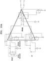
- FIGS. 10A to 10C are diagrams illustrating noise of a sensor interface of FIG. 1 .
- FIG. 10A is a circuit implementing the sensor interface of FIG. 1
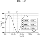
- FIG. 10B is a graph of an output signal of the sensor interface
- FIG. 10C illustrates a cumulative noise of the output signal of the sensor interface.
- the output signal of the sensor interface is 2.53 V at 118.16 ⁇ s, and 2.46 V at 369.8 ⁇ s, and the amplitude of the output signal is 70.5 mV.
- noise of the output signal accumulated while sensing a signal in the range of about 100Hz to about 10kHz is 42.24 ⁇ V.
- FIGS. 11A to 11C are diagrams illustrating noise of a sensor interface of FIG. 3 .
- FIG. 11A is a circuit implementing the sensor interface of FIG. 3
- FIG. 11B is a graph of an output signal of the sensor interface
- FIG. 11C illustrates a cumulative noise of the output signal of the sensor interface.
- the output signal of the sensor interface is 2.53 V at 118.16 ⁇ s, and 2.46 V at 369.8 ⁇ s, and the amplitude of the output signal is 70.5 mV.
- the noise of the output signal accumulated while sensing a signal in the range of about 100Hz to about 10kHz is 31.02 ⁇ V.
- the amplitude of the output signal of the sensor interface is the same as 70.5 mV, whereas the noise of the output signal is reduced by about 2 times from 42.24 ⁇ V to 31.02 ⁇ V. That is, an SNR increases by about 3dB. Therefore, the sensor interface may be configured by separating cantilever beam bundles such that an output signal with improved noise may be obtained without a change in the amplitude.
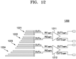
- FIG. 12 is a diagram illustrating a sensor interface 1200 according to an example embodiment.
- a sensor interface of FIG. 3 is configured as two separated cantilever beam bundles
- the sensor interface 1200 of FIG. 12 is configured as four separated cantilever beam bundles 1221 to 1224.
- the sensor interface 1200 includes the four cantilever beam bundles 1221 to 1224 and two differential amplifiers 1211 and 1212.
- the cantilever beam bundles 1221 to 1224 and the differential amplifiers 1211 and 1212 may include the configurations and functions of the cantilever beam bundle and the differential amplifier described in the above example embodiments, and thus redundant descriptions thereof will be omitted.
- the cantilever beam bundles 1221 to 1224 may be configured to filter signals of different frequency bands.
- the output terminal OUT F1 of the first cantilever beam bundle 1221 and the first input terminal IN1 AMP1 of the first differential amplifier 1211 may be electrically connected, and the output terminal OUT F2 of the second cantilever beam bundle 1222 and the second input terminal IN2 AMP1 of the first differential amplifier 1211 may be electrically connected.
- the third and fourth cantilever beam bundles 1223 and 1224 and the second differential amplifier 1212 may be connected in the same manner.
- the first and second differential amplifiers 1211 and 1212 may generate output signals by amplifying the filtered signals.
- the sensor interface may be configured as cantilever beam bundles separated into various numbers such as 8, 16, etc.
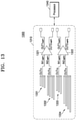
- FIG. 13 is a diagram illustrating a sound processing device 1300 according to an example embodiment.
- the sound processing device 1300 is a device that converts and processes a sound signal into an electrical signal, and may include a speaker, a microphone, an earphone, a bio device, a portable device, a TV, a vehicle device, an loT device, etc., but is not limited thereto.
- the sound processing device 1300 may include a sensor interface 1310 and a processor 1340 that processes an output signal of the sensor interface 1310.
- the sensor interface 1310 includes four cantilever beam bundles 1331 to 1334 and two differential amplifiers 1321 and 1322.
- the cantilever beam bundles 1331 to 1334 and the differential amplifiers 1321 and 1322 may include the configurations and functions of the cantilever beam bundle and the differential amplifier described in the above embodiments, and thus redundant descriptions thereof will be omitted.
- the cantilever beam bundles 1331 to 1334 may be configured to filter signals of different frequency bands.
- the order in which the cantilever beam bundles 1331 to 1334 are arranged may not be dependent on frequency bands of the signals filtered by the cantilever beam bundles 1331 to 1334.
- the first cantilever beam bundle 1331 may be configured to filter a sound signal in a frequency band in the range of about 2 kHz to about 20 kHz
- the second cantilever beam bundle 1332 may be configured to filter a sound signal in a frequency band in the range of about 100 Hz to about 1 kHz
- the third cantilever beam bundle 1333 may be configured to filter a sound signal in a frequency band in the range of about 1 kHz to about 2 kHz
- the fourth cantilever beam bundle 1334 may be configured to filter a sound signal in a frequency band in the range of about 20 Hz to about 100 Hz.
- the sensor interface 1310 may be configured as the sensor interface described above, for example, in FIG. 3 .
- the processor 1340 may be configured to process the output signal of the sensor interface 1310.
- the processor 1340 may be configured to select which output signal to process from an output signal through the first differential amplifier 1321 and an output signal through the second differential amplifier 1322.
- the processor 1340 may be implemented as an array of a plurality of logic gates, and may be implemented as a combination of a general-purpose microprocessor and a memory in which a program executable in the microprocessor is stored. Further, the processor 1340 may include a filter for filtering the output signal.
Landscapes
- Engineering & Computer Science (AREA)
- Physics & Mathematics (AREA)
- General Physics & Mathematics (AREA)
- Power Engineering (AREA)
- Acoustics & Sound (AREA)
- Signal Processing (AREA)
- Computer Hardware Design (AREA)
- Microelectronics & Electronic Packaging (AREA)
- Multimedia (AREA)
- Micromachines (AREA)
- Piezo-Electric Or Mechanical Vibrators, Or Delay Or Filter Circuits (AREA)
- Pressure Sensors (AREA)
Applications Claiming Priority (1)
| Application Number | Priority Date | Filing Date | Title |
|---|---|---|---|
| KR1020200120030A KR102827125B1 (ko) | 2020-09-17 | 2020-09-17 | 공진기 및 차동 증폭기를 포함하는 센서 인터페이스 |
Publications (2)
| Publication Number | Publication Date |
|---|---|
| EP3972128A1 true EP3972128A1 (fr) | 2022-03-23 |
| EP3972128B1 EP3972128B1 (fr) | 2023-10-04 |
Family
ID=75202974
Family Applications (1)
| Application Number | Title | Priority Date | Filing Date |
|---|---|---|---|
| EP21164252.5A Active EP3972128B1 (fr) | 2020-09-17 | 2021-03-23 | Interface de capteur comprenant un résonateur et un amplificateur différentiel |
Country Status (4)
| Country | Link |
|---|---|
| US (1) | US11770658B2 (fr) |
| EP (1) | EP3972128B1 (fr) |
| KR (1) | KR102827125B1 (fr) |
| CN (1) | CN114204916A (fr) |
Cited By (1)
| Publication number | Priority date | Publication date | Assignee | Title |
|---|---|---|---|---|
| EP4294049A4 (fr) * | 2022-04-27 | 2025-04-09 | Shenzhen Shokz Co., Ltd. | Dispositif de sortie acoustique |
Families Citing this family (1)
| Publication number | Priority date | Publication date | Assignee | Title |
|---|---|---|---|---|
| CN114964337B (zh) * | 2022-05-19 | 2024-05-31 | 上海迈振电子科技有限公司 | 一种微悬臂梁传感器信号放大装置及其数控系统 |
Citations (1)
| Publication number | Priority date | Publication date | Assignee | Title |
|---|---|---|---|---|
| EP0959333A2 (fr) * | 1998-05-22 | 1999-11-24 | Sumitomo Metal Industries Limited | Méthode et dispositif por détecter des ondes de vibrations |
Family Cites Families (18)
| Publication number | Priority date | Publication date | Assignee | Title |
|---|---|---|---|---|
| KR100470708B1 (ko) * | 2003-05-22 | 2005-03-10 | 삼성전자주식회사 | 금속막의 내부응력을 이용한 박막 벌크 음향 공진기제조방법 및 그에 의한 공진기 |
| JP4256367B2 (ja) * | 2005-07-06 | 2009-04-22 | 東京エレクトロン株式会社 | 振動波検出装置 |
| JP4382740B2 (ja) * | 2005-10-21 | 2009-12-16 | トヨタ自動車株式会社 | フードエアバッグ装置 |
| KR100736894B1 (ko) | 2006-03-27 | 2007-07-10 | 송기무 | 다채널 진동판이 구비된 전기-음향 변환장치 및 이를이용한 보청기 |
| JP4539920B2 (ja) | 2006-05-12 | 2010-09-08 | 国立大学法人 東京大学 | 振動波検出方法及び装置 |
| KR100999838B1 (ko) * | 2008-05-09 | 2010-12-09 | 한국과학기술원 | 다중외팔보 mems 센서의 제조방법 및 다중외팔보 mems 센서를 이용한 음원위치 추정방법 |
| CN104602170B (zh) | 2008-06-30 | 2019-08-13 | 密歇根大学董事会 | 压电mems麦克风 |
| US20100117485A1 (en) * | 2008-11-13 | 2010-05-13 | Avago Technologies Wireless Ip (Singapore) Pte. Ltd. | Piezoelectric transducers with noise-cancelling electrodes |
| JP2013190362A (ja) | 2012-03-14 | 2013-09-26 | Kazuo Muto | Aeセンサの製造方法およびこれによって製造されたaeセンサ |
| US10165342B2 (en) * | 2014-05-12 | 2018-12-25 | Tdk Corporation | Microphone assembly and method of manufacturing a microphone assembly |
| KR102207928B1 (ko) | 2014-08-13 | 2021-01-26 | 삼성전자주식회사 | 음향 센싱 소자 및 주파수 정보 획득 방법 |
| US10063978B2 (en) * | 2016-09-13 | 2018-08-28 | Akustica, Inc. | Cantilevered shear resonance microphone |
| KR102715031B1 (ko) * | 2016-10-05 | 2024-10-10 | 삼성전자주식회사 | 공진기를 포함하는 필터 시스템 |
| KR102364853B1 (ko) * | 2017-07-18 | 2022-02-18 | 삼성전자주식회사 | 음향 센싱 소자의 신호 처리 방법과 음향 센싱 시스템 |
| WO2019021047A1 (fr) | 2017-07-26 | 2019-01-31 | King Abdullah University Of Science And Technology | Filtre passe-bande basé sur mems |
| KR102335774B1 (ko) * | 2017-09-01 | 2021-12-06 | 삼성전자주식회사 | 다중 공진기 어레이를 포함하는 소리 방향 탐지 센서 |
| KR102623514B1 (ko) | 2017-10-23 | 2024-01-11 | 삼성전자주식회사 | 음성신호 처리장치 및 그 동작방법 |
| KR102395994B1 (ko) * | 2017-12-27 | 2022-05-11 | 삼성전자주식회사 | 지향성 마이크로폰 |
-
2020
- 2020-09-17 KR KR1020200120030A patent/KR102827125B1/ko active Active
-
2021
- 2021-02-23 CN CN202110202648.7A patent/CN114204916A/zh active Pending
- 2021-02-23 US US17/182,911 patent/US11770658B2/en active Active
- 2021-03-23 EP EP21164252.5A patent/EP3972128B1/fr active Active
Patent Citations (1)
| Publication number | Priority date | Publication date | Assignee | Title |
|---|---|---|---|---|
| EP0959333A2 (fr) * | 1998-05-22 | 1999-11-24 | Sumitomo Metal Industries Limited | Méthode et dispositif por détecter des ondes de vibrations |
Cited By (1)
| Publication number | Priority date | Publication date | Assignee | Title |
|---|---|---|---|---|
| EP4294049A4 (fr) * | 2022-04-27 | 2025-04-09 | Shenzhen Shokz Co., Ltd. | Dispositif de sortie acoustique |
Also Published As
| Publication number | Publication date |
|---|---|
| CN114204916A (zh) | 2022-03-18 |
| EP3972128B1 (fr) | 2023-10-04 |
| US20220086570A1 (en) | 2022-03-17 |
| KR102827125B1 (ko) | 2025-07-03 |
| KR20220037551A (ko) | 2022-03-25 |
| US11770658B2 (en) | 2023-09-26 |
Similar Documents
| Publication | Publication Date | Title |
|---|---|---|
| US10926999B2 (en) | Microelectromechanical transducer | |
| US10477322B2 (en) | MEMS device and process | |
| US12289095B2 (en) | Filter system including resonator | |
| JP6830527B2 (ja) | 圧電マイクロフォンチップおよび圧電マイクロフォン | |
| KR102475893B1 (ko) | 음향/진동 스펙트럼 분석 소자 및 주파수 정보 획득 및 분석 방법 | |
| US11892466B2 (en) | Piezoelectric accelerometer with wake function | |
| KR102364853B1 (ko) | 음향 센싱 소자의 신호 처리 방법과 음향 센싱 시스템 | |
| US9693150B2 (en) | Microphone sensor | |
| US10684163B2 (en) | Acoustic wave sensor | |
| JP2010232971A (ja) | マイクロホン装置並びにその調整装置及び調整方法 | |
| EP3972128B1 (fr) | Interface de capteur comprenant un résonateur et un amplificateur différentiel | |
| US11146240B2 (en) | Micromechanical resonator and resonator system including the same | |
| US20060113879A1 (en) | Piezoelectric micro acoustic sensor based on ferroelectric materials | |
| JP2018179626A (ja) | 超音波受信器 | |
| JP6867789B2 (ja) | Memsマイクロフォン | |
| JP6844911B2 (ja) | 圧電素子 | |
| JP4672539B2 (ja) | コンデンサマイクロホン装置 | |
| CN119854717A (zh) | 一种微机电系统压电传感器和压电麦克风 | |
| JP2016095177A (ja) | 加速度センサ |
Legal Events
| Date | Code | Title | Description |
|---|---|---|---|
| PUAI | Public reference made under article 153(3) epc to a published international application that has entered the european phase |
Free format text: ORIGINAL CODE: 0009012 |
|
| STAA | Information on the status of an ep patent application or granted ep patent |
Free format text: STATUS: REQUEST FOR EXAMINATION WAS MADE |
|
| 17P | Request for examination filed |
Effective date: 20220208 |
|
| AK | Designated contracting states |
Kind code of ref document: A1 Designated state(s): AL AT BE BG CH CY CZ DE DK EE ES FI FR GB GR HR HU IE IS IT LI LT LU LV MC MK MT NL NO PL PT RO RS SE SI SK SM TR |
|
| GRAP | Despatch of communication of intention to grant a patent |
Free format text: ORIGINAL CODE: EPIDOSNIGR1 |
|
| STAA | Information on the status of an ep patent application or granted ep patent |
Free format text: STATUS: GRANT OF PATENT IS INTENDED |
|
| INTG | Intention to grant announced |
Effective date: 20230417 |
|
| P01 | Opt-out of the competence of the unified patent court (upc) registered |
Effective date: 20230520 |
|
| GRAS | Grant fee paid |
Free format text: ORIGINAL CODE: EPIDOSNIGR3 |
|
| GRAA | (expected) grant |
Free format text: ORIGINAL CODE: 0009210 |
|
| STAA | Information on the status of an ep patent application or granted ep patent |
Free format text: STATUS: THE PATENT HAS BEEN GRANTED |
|
| AK | Designated contracting states |
Kind code of ref document: B1 Designated state(s): AL AT BE BG CH CY CZ DE DK EE ES FI FR GB GR HR HU IE IS IT LI LT LU LV MC MK MT NL NO PL PT RO RS SE SI SK SM TR |
|
| REG | Reference to a national code |
Ref country code: GB Ref legal event code: FG4D |
|
| REG | Reference to a national code |
Ref country code: CH Ref legal event code: EP |
|
| REG | Reference to a national code |
Ref country code: IE Ref legal event code: FG4D |
|
| REG | Reference to a national code |
Ref country code: DE Ref legal event code: R096 Ref document number: 602021005528 Country of ref document: DE |
|
| REG | Reference to a national code |
Ref country code: LT Ref legal event code: MG9D |
|
| REG | Reference to a national code |
Ref country code: NL Ref legal event code: MP Effective date: 20231004 |
|
| REG | Reference to a national code |
Ref country code: AT Ref legal event code: MK05 Ref document number: 1618805 Country of ref document: AT Kind code of ref document: T Effective date: 20231004 |
|
| PG25 | Lapsed in a contracting state [announced via postgrant information from national office to epo] |
Ref country code: NL Free format text: LAPSE BECAUSE OF FAILURE TO SUBMIT A TRANSLATION OF THE DESCRIPTION OR TO PAY THE FEE WITHIN THE PRESCRIBED TIME-LIMIT Effective date: 20231004 |
|
| PG25 | Lapsed in a contracting state [announced via postgrant information from national office to epo] |
Ref country code: GR Free format text: LAPSE BECAUSE OF FAILURE TO SUBMIT A TRANSLATION OF THE DESCRIPTION OR TO PAY THE FEE WITHIN THE PRESCRIBED TIME-LIMIT Effective date: 20240105 |
|
| PG25 | Lapsed in a contracting state [announced via postgrant information from national office to epo] |
Ref country code: IS Free format text: LAPSE BECAUSE OF FAILURE TO SUBMIT A TRANSLATION OF THE DESCRIPTION OR TO PAY THE FEE WITHIN THE PRESCRIBED TIME-LIMIT Effective date: 20240204 |
|
| PG25 | Lapsed in a contracting state [announced via postgrant information from national office to epo] |
Ref country code: LT Free format text: LAPSE BECAUSE OF FAILURE TO SUBMIT A TRANSLATION OF THE DESCRIPTION OR TO PAY THE FEE WITHIN THE PRESCRIBED TIME-LIMIT Effective date: 20231004 |
|
| PG25 | Lapsed in a contracting state [announced via postgrant information from national office to epo] |
Ref country code: AT Free format text: LAPSE BECAUSE OF FAILURE TO SUBMIT A TRANSLATION OF THE DESCRIPTION OR TO PAY THE FEE WITHIN THE PRESCRIBED TIME-LIMIT Effective date: 20231004 |
|
| PG25 | Lapsed in a contracting state [announced via postgrant information from national office to epo] |
Ref country code: ES Free format text: LAPSE BECAUSE OF FAILURE TO SUBMIT A TRANSLATION OF THE DESCRIPTION OR TO PAY THE FEE WITHIN THE PRESCRIBED TIME-LIMIT Effective date: 20231004 |
|
| PG25 | Lapsed in a contracting state [announced via postgrant information from national office to epo] |
Ref country code: LT Free format text: LAPSE BECAUSE OF FAILURE TO SUBMIT A TRANSLATION OF THE DESCRIPTION OR TO PAY THE FEE WITHIN THE PRESCRIBED TIME-LIMIT Effective date: 20231004 Ref country code: IS Free format text: LAPSE BECAUSE OF FAILURE TO SUBMIT A TRANSLATION OF THE DESCRIPTION OR TO PAY THE FEE WITHIN THE PRESCRIBED TIME-LIMIT Effective date: 20240204 Ref country code: GR Free format text: LAPSE BECAUSE OF FAILURE TO SUBMIT A TRANSLATION OF THE DESCRIPTION OR TO PAY THE FEE WITHIN THE PRESCRIBED TIME-LIMIT Effective date: 20240105 Ref country code: ES Free format text: LAPSE BECAUSE OF FAILURE TO SUBMIT A TRANSLATION OF THE DESCRIPTION OR TO PAY THE FEE WITHIN THE PRESCRIBED TIME-LIMIT Effective date: 20231004 Ref country code: BG Free format text: LAPSE BECAUSE OF FAILURE TO SUBMIT A TRANSLATION OF THE DESCRIPTION OR TO PAY THE FEE WITHIN THE PRESCRIBED TIME-LIMIT Effective date: 20240104 Ref country code: AT Free format text: LAPSE BECAUSE OF FAILURE TO SUBMIT A TRANSLATION OF THE DESCRIPTION OR TO PAY THE FEE WITHIN THE PRESCRIBED TIME-LIMIT Effective date: 20231004 Ref country code: PT Free format text: LAPSE BECAUSE OF FAILURE TO SUBMIT A TRANSLATION OF THE DESCRIPTION OR TO PAY THE FEE WITHIN THE PRESCRIBED TIME-LIMIT Effective date: 20240205 |
|
| PG25 | Lapsed in a contracting state [announced via postgrant information from national office to epo] |
Ref country code: SE Free format text: LAPSE BECAUSE OF FAILURE TO SUBMIT A TRANSLATION OF THE DESCRIPTION OR TO PAY THE FEE WITHIN THE PRESCRIBED TIME-LIMIT Effective date: 20231004 Ref country code: RS Free format text: LAPSE BECAUSE OF FAILURE TO SUBMIT A TRANSLATION OF THE DESCRIPTION OR TO PAY THE FEE WITHIN THE PRESCRIBED TIME-LIMIT Effective date: 20231004 Ref country code: PL Free format text: LAPSE BECAUSE OF FAILURE TO SUBMIT A TRANSLATION OF THE DESCRIPTION OR TO PAY THE FEE WITHIN THE PRESCRIBED TIME-LIMIT Effective date: 20231004 Ref country code: NO Free format text: LAPSE BECAUSE OF FAILURE TO SUBMIT A TRANSLATION OF THE DESCRIPTION OR TO PAY THE FEE WITHIN THE PRESCRIBED TIME-LIMIT Effective date: 20240104 Ref country code: LV Free format text: LAPSE BECAUSE OF FAILURE TO SUBMIT A TRANSLATION OF THE DESCRIPTION OR TO PAY THE FEE WITHIN THE PRESCRIBED TIME-LIMIT Effective date: 20231004 Ref country code: HR Free format text: LAPSE BECAUSE OF FAILURE TO SUBMIT A TRANSLATION OF THE DESCRIPTION OR TO PAY THE FEE WITHIN THE PRESCRIBED TIME-LIMIT Effective date: 20231004 |
|
| REG | Reference to a national code |
Ref country code: DE Ref legal event code: R097 Ref document number: 602021005528 Country of ref document: DE |
|
| PG25 | Lapsed in a contracting state [announced via postgrant information from national office to epo] |
Ref country code: DK Free format text: LAPSE BECAUSE OF FAILURE TO SUBMIT A TRANSLATION OF THE DESCRIPTION OR TO PAY THE FEE WITHIN THE PRESCRIBED TIME-LIMIT Effective date: 20231004 |
|
| PG25 | Lapsed in a contracting state [announced via postgrant information from national office to epo] |
Ref country code: CZ Free format text: LAPSE BECAUSE OF FAILURE TO SUBMIT A TRANSLATION OF THE DESCRIPTION OR TO PAY THE FEE WITHIN THE PRESCRIBED TIME-LIMIT Effective date: 20231004 |
|
| PG25 | Lapsed in a contracting state [announced via postgrant information from national office to epo] |
Ref country code: SK Free format text: LAPSE BECAUSE OF FAILURE TO SUBMIT A TRANSLATION OF THE DESCRIPTION OR TO PAY THE FEE WITHIN THE PRESCRIBED TIME-LIMIT Effective date: 20231004 |
|
| PG25 | Lapsed in a contracting state [announced via postgrant information from national office to epo] |
Ref country code: SM Free format text: LAPSE BECAUSE OF FAILURE TO SUBMIT A TRANSLATION OF THE DESCRIPTION OR TO PAY THE FEE WITHIN THE PRESCRIBED TIME-LIMIT Effective date: 20231004 Ref country code: SK Free format text: LAPSE BECAUSE OF FAILURE TO SUBMIT A TRANSLATION OF THE DESCRIPTION OR TO PAY THE FEE WITHIN THE PRESCRIBED TIME-LIMIT Effective date: 20231004 Ref country code: RO Free format text: LAPSE BECAUSE OF FAILURE TO SUBMIT A TRANSLATION OF THE DESCRIPTION OR TO PAY THE FEE WITHIN THE PRESCRIBED TIME-LIMIT Effective date: 20231004 Ref country code: IT Free format text: LAPSE BECAUSE OF FAILURE TO SUBMIT A TRANSLATION OF THE DESCRIPTION OR TO PAY THE FEE WITHIN THE PRESCRIBED TIME-LIMIT Effective date: 20231004 Ref country code: EE Free format text: LAPSE BECAUSE OF FAILURE TO SUBMIT A TRANSLATION OF THE DESCRIPTION OR TO PAY THE FEE WITHIN THE PRESCRIBED TIME-LIMIT Effective date: 20231004 Ref country code: DK Free format text: LAPSE BECAUSE OF FAILURE TO SUBMIT A TRANSLATION OF THE DESCRIPTION OR TO PAY THE FEE WITHIN THE PRESCRIBED TIME-LIMIT Effective date: 20231004 Ref country code: CZ Free format text: LAPSE BECAUSE OF FAILURE TO SUBMIT A TRANSLATION OF THE DESCRIPTION OR TO PAY THE FEE WITHIN THE PRESCRIBED TIME-LIMIT Effective date: 20231004 |
|
| PLBE | No opposition filed within time limit |
Free format text: ORIGINAL CODE: 0009261 |
|
| STAA | Information on the status of an ep patent application or granted ep patent |
Free format text: STATUS: NO OPPOSITION FILED WITHIN TIME LIMIT |
|
| 26N | No opposition filed |
Effective date: 20240705 |
|
| PG25 | Lapsed in a contracting state [announced via postgrant information from national office to epo] |
Ref country code: SI Free format text: LAPSE BECAUSE OF FAILURE TO SUBMIT A TRANSLATION OF THE DESCRIPTION OR TO PAY THE FEE WITHIN THE PRESCRIBED TIME-LIMIT Effective date: 20231004 |
|
| PG25 | Lapsed in a contracting state [announced via postgrant information from national office to epo] |
Ref country code: SI Free format text: LAPSE BECAUSE OF FAILURE TO SUBMIT A TRANSLATION OF THE DESCRIPTION OR TO PAY THE FEE WITHIN THE PRESCRIBED TIME-LIMIT Effective date: 20231004 |
|
| REG | Reference to a national code |
Ref country code: CH Ref legal event code: PL |
|
| PG25 | Lapsed in a contracting state [announced via postgrant information from national office to epo] |
Ref country code: LU Free format text: LAPSE BECAUSE OF NON-PAYMENT OF DUE FEES Effective date: 20240323 |
|
| PG25 | Lapsed in a contracting state [announced via postgrant information from national office to epo] |
Ref country code: MC Free format text: LAPSE BECAUSE OF FAILURE TO SUBMIT A TRANSLATION OF THE DESCRIPTION OR TO PAY THE FEE WITHIN THE PRESCRIBED TIME-LIMIT Effective date: 20231004 |
|
| PG25 | Lapsed in a contracting state [announced via postgrant information from national office to epo] |
Ref country code: MC Free format text: LAPSE BECAUSE OF FAILURE TO SUBMIT A TRANSLATION OF THE DESCRIPTION OR TO PAY THE FEE WITHIN THE PRESCRIBED TIME-LIMIT Effective date: 20231004 Ref country code: LU Free format text: LAPSE BECAUSE OF NON-PAYMENT OF DUE FEES Effective date: 20240323 |
|
| REG | Reference to a national code |
Ref country code: BE Ref legal event code: MM Effective date: 20240331 |
|
| PG25 | Lapsed in a contracting state [announced via postgrant information from national office to epo] |
Ref country code: BE Free format text: LAPSE BECAUSE OF NON-PAYMENT OF DUE FEES Effective date: 20240331 |
|
| PG25 | Lapsed in a contracting state [announced via postgrant information from national office to epo] |
Ref country code: IE Free format text: LAPSE BECAUSE OF NON-PAYMENT OF DUE FEES Effective date: 20240323 |
|
| PG25 | Lapsed in a contracting state [announced via postgrant information from national office to epo] |
Ref country code: IE Free format text: LAPSE BECAUSE OF NON-PAYMENT OF DUE FEES Effective date: 20240323 Ref country code: BE Free format text: LAPSE BECAUSE OF NON-PAYMENT OF DUE FEES Effective date: 20240331 Ref country code: CH Free format text: LAPSE BECAUSE OF NON-PAYMENT OF DUE FEES Effective date: 20240331 |
|
| PG25 | Lapsed in a contracting state [announced via postgrant information from national office to epo] |
Ref country code: CY Free format text: LAPSE BECAUSE OF FAILURE TO SUBMIT A TRANSLATION OF THE DESCRIPTION OR TO PAY THE FEE WITHIN THE PRESCRIBED TIME-LIMIT; INVALID AB INITIO Effective date: 20210323 |
|
| PG25 | Lapsed in a contracting state [announced via postgrant information from national office to epo] |
Ref country code: HU Free format text: LAPSE BECAUSE OF FAILURE TO SUBMIT A TRANSLATION OF THE DESCRIPTION OR TO PAY THE FEE WITHIN THE PRESCRIBED TIME-LIMIT; INVALID AB INITIO Effective date: 20210323 |
|
| PG25 | Lapsed in a contracting state [announced via postgrant information from national office to epo] |
Ref country code: FI Free format text: LAPSE BECAUSE OF FAILURE TO SUBMIT A TRANSLATION OF THE DESCRIPTION OR TO PAY THE FEE WITHIN THE PRESCRIBED TIME-LIMIT Effective date: 20231004 |
|
| PG25 | Lapsed in a contracting state [announced via postgrant information from national office to epo] |
Ref country code: TR Free format text: LAPSE BECAUSE OF FAILURE TO SUBMIT A TRANSLATION OF THE DESCRIPTION OR TO PAY THE FEE WITHIN THE PRESCRIBED TIME-LIMIT Effective date: 20231004 |
|
| PGFP | Annual fee paid to national office [announced via postgrant information from national office to epo] |
Ref country code: GB Payment date: 20260216 Year of fee payment: 6 |
|
| PGFP | Annual fee paid to national office [announced via postgrant information from national office to epo] |
Ref country code: DE Payment date: 20260211 Year of fee payment: 6 |
|
| PGFP | Annual fee paid to national office [announced via postgrant information from national office to epo] |
Ref country code: FR Payment date: 20260209 Year of fee payment: 6 |