EP3977295B1 - Cache victime prenant en charge des entrées écriture de justesse de vidage - Google Patents
Cache victime prenant en charge des entrées écriture de justesse de vidage Download PDFInfo
- Publication number
- EP3977295B1 EP3977295B1 EP20812543.5A EP20812543A EP3977295B1 EP 3977295 B1 EP3977295 B1 EP 3977295B1 EP 20812543 A EP20812543 A EP 20812543A EP 3977295 B1 EP3977295 B1 EP 3977295B1
- Authority
- EP
- European Patent Office
- Prior art keywords
- cache
- write
- memory
- sub
- miss
- Prior art date
- Legal status (The legal status is an assumption and is not a legal conclusion. Google has not performed a legal analysis and makes no representation as to the accuracy of the status listed.)
- Active
Links
Images




Classifications
-
- G—PHYSICS
- G06—COMPUTING OR CALCULATING; COUNTING
- G06F—ELECTRIC DIGITAL DATA PROCESSING
- G06F12/00—Accessing, addressing or allocating within memory systems or architectures
- G06F12/02—Addressing or allocation; Relocation
- G06F12/08—Addressing or allocation; Relocation in hierarchically structured memory systems, e.g. virtual memory systems
- G06F12/12—Replacement control
- G06F12/121—Replacement control using replacement algorithms
- G06F12/128—Replacement control using replacement algorithms adapted to multidimensional cache systems, e.g. set-associative, multicache, multiset or multilevel
-
- G—PHYSICS
- G06—COMPUTING OR CALCULATING; COUNTING
- G06F—ELECTRIC DIGITAL DATA PROCESSING
- G06F11/00—Error detection; Error correction; Monitoring
- G06F11/07—Responding to the occurrence of a fault, e.g. fault tolerance
- G06F11/08—Error detection or correction by redundancy in data representation, e.g. by using checking codes
- G06F11/10—Adding special bits or symbols to the coded information, e.g. parity check, casting out 9's or 11's
- G06F11/1008—Adding special bits or symbols to the coded information, e.g. parity check, casting out 9's or 11's in individual solid state devices
- G06F11/1064—Adding special bits or symbols to the coded information, e.g. parity check, casting out 9's or 11's in individual solid state devices in cache or content addressable memories
-
- G—PHYSICS
- G06—COMPUTING OR CALCULATING; COUNTING
- G06F—ELECTRIC DIGITAL DATA PROCESSING
- G06F12/00—Accessing, addressing or allocating within memory systems or architectures
- G06F12/02—Addressing or allocation; Relocation
- G06F12/0215—Addressing or allocation; Relocation with look ahead addressing means
-
- G—PHYSICS
- G06—COMPUTING OR CALCULATING; COUNTING
- G06F—ELECTRIC DIGITAL DATA PROCESSING
- G06F12/00—Accessing, addressing or allocating within memory systems or architectures
- G06F12/02—Addressing or allocation; Relocation
- G06F12/0223—User address space allocation, e.g. contiguous or non contiguous base addressing
- G06F12/023—Free address space management
- G06F12/0238—Memory management in non-volatile memory, e.g. resistive RAM or ferroelectric memory
-
- G—PHYSICS
- G06—COMPUTING OR CALCULATING; COUNTING
- G06F—ELECTRIC DIGITAL DATA PROCESSING
- G06F12/00—Accessing, addressing or allocating within memory systems or architectures
- G06F12/02—Addressing or allocation; Relocation
- G06F12/0223—User address space allocation, e.g. contiguous or non contiguous base addressing
- G06F12/0292—User address space allocation, e.g. contiguous or non contiguous base addressing using tables or multilevel address translation means
-
- G—PHYSICS
- G06—COMPUTING OR CALCULATING; COUNTING
- G06F—ELECTRIC DIGITAL DATA PROCESSING
- G06F12/00—Accessing, addressing or allocating within memory systems or architectures
- G06F12/02—Addressing or allocation; Relocation
- G06F12/08—Addressing or allocation; Relocation in hierarchically structured memory systems, e.g. virtual memory systems
- G06F12/0802—Addressing of a memory level in which the access to the desired data or data block requires associative addressing means, e.g. caches
-
- G—PHYSICS
- G06—COMPUTING OR CALCULATING; COUNTING
- G06F—ELECTRIC DIGITAL DATA PROCESSING
- G06F12/00—Accessing, addressing or allocating within memory systems or architectures
- G06F12/02—Addressing or allocation; Relocation
- G06F12/08—Addressing or allocation; Relocation in hierarchically structured memory systems, e.g. virtual memory systems
- G06F12/0802—Addressing of a memory level in which the access to the desired data or data block requires associative addressing means, e.g. caches
- G06F12/0804—Addressing of a memory level in which the access to the desired data or data block requires associative addressing means, e.g. caches with main memory updating
-
- G—PHYSICS
- G06—COMPUTING OR CALCULATING; COUNTING
- G06F—ELECTRIC DIGITAL DATA PROCESSING
- G06F12/00—Accessing, addressing or allocating within memory systems or architectures
- G06F12/02—Addressing or allocation; Relocation
- G06F12/08—Addressing or allocation; Relocation in hierarchically structured memory systems, e.g. virtual memory systems
- G06F12/0802—Addressing of a memory level in which the access to the desired data or data block requires associative addressing means, e.g. caches
- G06F12/0806—Multiuser, multiprocessor or multiprocessing cache systems
-
- G—PHYSICS
- G06—COMPUTING OR CALCULATING; COUNTING
- G06F—ELECTRIC DIGITAL DATA PROCESSING
- G06F12/00—Accessing, addressing or allocating within memory systems or architectures
- G06F12/02—Addressing or allocation; Relocation
- G06F12/08—Addressing or allocation; Relocation in hierarchically structured memory systems, e.g. virtual memory systems
- G06F12/0802—Addressing of a memory level in which the access to the desired data or data block requires associative addressing means, e.g. caches
- G06F12/0806—Multiuser, multiprocessor or multiprocessing cache systems
- G06F12/0811—Multiuser, multiprocessor or multiprocessing cache systems with multilevel cache hierarchies
-
- G—PHYSICS
- G06—COMPUTING OR CALCULATING; COUNTING
- G06F—ELECTRIC DIGITAL DATA PROCESSING
- G06F12/00—Accessing, addressing or allocating within memory systems or architectures
- G06F12/02—Addressing or allocation; Relocation
- G06F12/08—Addressing or allocation; Relocation in hierarchically structured memory systems, e.g. virtual memory systems
- G06F12/0802—Addressing of a memory level in which the access to the desired data or data block requires associative addressing means, e.g. caches
- G06F12/0806—Multiuser, multiprocessor or multiprocessing cache systems
- G06F12/0815—Cache consistency protocols
-
- G—PHYSICS
- G06—COMPUTING OR CALCULATING; COUNTING
- G06F—ELECTRIC DIGITAL DATA PROCESSING
- G06F12/00—Accessing, addressing or allocating within memory systems or architectures
- G06F12/02—Addressing or allocation; Relocation
- G06F12/08—Addressing or allocation; Relocation in hierarchically structured memory systems, e.g. virtual memory systems
- G06F12/0802—Addressing of a memory level in which the access to the desired data or data block requires associative addressing means, e.g. caches
- G06F12/0806—Multiuser, multiprocessor or multiprocessing cache systems
- G06F12/0815—Cache consistency protocols
- G06F12/0817—Cache consistency protocols using directory methods
- G06F12/082—Associative directories
-
- G—PHYSICS
- G06—COMPUTING OR CALCULATING; COUNTING
- G06F—ELECTRIC DIGITAL DATA PROCESSING
- G06F12/00—Accessing, addressing or allocating within memory systems or architectures
- G06F12/02—Addressing or allocation; Relocation
- G06F12/08—Addressing or allocation; Relocation in hierarchically structured memory systems, e.g. virtual memory systems
- G06F12/0802—Addressing of a memory level in which the access to the desired data or data block requires associative addressing means, e.g. caches
- G06F12/0844—Multiple simultaneous or quasi-simultaneous cache accessing
- G06F12/0853—Cache with multiport tag or data arrays
-
- G—PHYSICS
- G06—COMPUTING OR CALCULATING; COUNTING
- G06F—ELECTRIC DIGITAL DATA PROCESSING
- G06F12/00—Accessing, addressing or allocating within memory systems or architectures
- G06F12/02—Addressing or allocation; Relocation
- G06F12/08—Addressing or allocation; Relocation in hierarchically structured memory systems, e.g. virtual memory systems
- G06F12/0802—Addressing of a memory level in which the access to the desired data or data block requires associative addressing means, e.g. caches
- G06F12/0844—Multiple simultaneous or quasi-simultaneous cache accessing
- G06F12/0855—Overlapped cache accessing, e.g. pipeline
-
- G—PHYSICS
- G06—COMPUTING OR CALCULATING; COUNTING
- G06F—ELECTRIC DIGITAL DATA PROCESSING
- G06F12/00—Accessing, addressing or allocating within memory systems or architectures
- G06F12/02—Addressing or allocation; Relocation
- G06F12/08—Addressing or allocation; Relocation in hierarchically structured memory systems, e.g. virtual memory systems
- G06F12/0802—Addressing of a memory level in which the access to the desired data or data block requires associative addressing means, e.g. caches
- G06F12/0864—Addressing of a memory level in which the access to the desired data or data block requires associative addressing means, e.g. caches using pseudo-associative means, e.g. set-associative or hashing
-
- G—PHYSICS
- G06—COMPUTING OR CALCULATING; COUNTING
- G06F—ELECTRIC DIGITAL DATA PROCESSING
- G06F12/00—Accessing, addressing or allocating within memory systems or architectures
- G06F12/02—Addressing or allocation; Relocation
- G06F12/08—Addressing or allocation; Relocation in hierarchically structured memory systems, e.g. virtual memory systems
- G06F12/0802—Addressing of a memory level in which the access to the desired data or data block requires associative addressing means, e.g. caches
- G06F12/0877—Cache access modes
- G06F12/0884—Parallel mode, e.g. in parallel with main memory or CPU
-
- G—PHYSICS
- G06—COMPUTING OR CALCULATING; COUNTING
- G06F—ELECTRIC DIGITAL DATA PROCESSING
- G06F12/00—Accessing, addressing or allocating within memory systems or architectures
- G06F12/02—Addressing or allocation; Relocation
- G06F12/08—Addressing or allocation; Relocation in hierarchically structured memory systems, e.g. virtual memory systems
- G06F12/0802—Addressing of a memory level in which the access to the desired data or data block requires associative addressing means, e.g. caches
- G06F12/0888—Addressing of a memory level in which the access to the desired data or data block requires associative addressing means, e.g. caches using selective caching, e.g. bypass
-
- G—PHYSICS
- G06—COMPUTING OR CALCULATING; COUNTING
- G06F—ELECTRIC DIGITAL DATA PROCESSING
- G06F12/00—Accessing, addressing or allocating within memory systems or architectures
- G06F12/02—Addressing or allocation; Relocation
- G06F12/08—Addressing or allocation; Relocation in hierarchically structured memory systems, e.g. virtual memory systems
- G06F12/0802—Addressing of a memory level in which the access to the desired data or data block requires associative addressing means, e.g. caches
- G06F12/0891—Addressing of a memory level in which the access to the desired data or data block requires associative addressing means, e.g. caches using clearing, invalidating or resetting means
-
- G—PHYSICS
- G06—COMPUTING OR CALCULATING; COUNTING
- G06F—ELECTRIC DIGITAL DATA PROCESSING
- G06F12/00—Accessing, addressing or allocating within memory systems or architectures
- G06F12/02—Addressing or allocation; Relocation
- G06F12/08—Addressing or allocation; Relocation in hierarchically structured memory systems, e.g. virtual memory systems
- G06F12/0802—Addressing of a memory level in which the access to the desired data or data block requires associative addressing means, e.g. caches
- G06F12/0893—Caches characterised by their organisation or structure
- G06F12/0895—Caches characterised by their organisation or structure of parts of caches, e.g. directory or tag array
-
- G—PHYSICS
- G06—COMPUTING OR CALCULATING; COUNTING
- G06F—ELECTRIC DIGITAL DATA PROCESSING
- G06F12/00—Accessing, addressing or allocating within memory systems or architectures
- G06F12/02—Addressing or allocation; Relocation
- G06F12/08—Addressing or allocation; Relocation in hierarchically structured memory systems, e.g. virtual memory systems
- G06F12/0802—Addressing of a memory level in which the access to the desired data or data block requires associative addressing means, e.g. caches
- G06F12/0893—Caches characterised by their organisation or structure
- G06F12/0897—Caches characterised by their organisation or structure with two or more cache hierarchy levels
-
- G—PHYSICS
- G06—COMPUTING OR CALCULATING; COUNTING
- G06F—ELECTRIC DIGITAL DATA PROCESSING
- G06F12/00—Accessing, addressing or allocating within memory systems or architectures
- G06F12/02—Addressing or allocation; Relocation
- G06F12/08—Addressing or allocation; Relocation in hierarchically structured memory systems, e.g. virtual memory systems
- G06F12/10—Address translation
- G06F12/1027—Address translation using associative or pseudo-associative address translation means, e.g. translation look-aside buffer [TLB]
-
- G—PHYSICS
- G06—COMPUTING OR CALCULATING; COUNTING
- G06F—ELECTRIC DIGITAL DATA PROCESSING
- G06F12/00—Accessing, addressing or allocating within memory systems or architectures
- G06F12/02—Addressing or allocation; Relocation
- G06F12/08—Addressing or allocation; Relocation in hierarchically structured memory systems, e.g. virtual memory systems
- G06F12/12—Replacement control
-
- G—PHYSICS
- G06—COMPUTING OR CALCULATING; COUNTING
- G06F—ELECTRIC DIGITAL DATA PROCESSING
- G06F12/00—Accessing, addressing or allocating within memory systems or architectures
- G06F12/02—Addressing or allocation; Relocation
- G06F12/08—Addressing or allocation; Relocation in hierarchically structured memory systems, e.g. virtual memory systems
- G06F12/12—Replacement control
- G06F12/121—Replacement control using replacement algorithms
-
- G—PHYSICS
- G06—COMPUTING OR CALCULATING; COUNTING
- G06F—ELECTRIC DIGITAL DATA PROCESSING
- G06F12/00—Accessing, addressing or allocating within memory systems or architectures
- G06F12/02—Addressing or allocation; Relocation
- G06F12/08—Addressing or allocation; Relocation in hierarchically structured memory systems, e.g. virtual memory systems
- G06F12/12—Replacement control
- G06F12/121—Replacement control using replacement algorithms
- G06F12/126—Replacement control using replacement algorithms with special data handling, e.g. priority of data or instructions, handling errors or pinning
-
- G—PHYSICS
- G06—COMPUTING OR CALCULATING; COUNTING
- G06F—ELECTRIC DIGITAL DATA PROCESSING
- G06F12/00—Accessing, addressing or allocating within memory systems or architectures
- G06F12/02—Addressing or allocation; Relocation
- G06F12/08—Addressing or allocation; Relocation in hierarchically structured memory systems, e.g. virtual memory systems
- G06F12/12—Replacement control
- G06F12/121—Replacement control using replacement algorithms
- G06F12/126—Replacement control using replacement algorithms with special data handling, e.g. priority of data or instructions, handling errors or pinning
- G06F12/127—Replacement control using replacement algorithms with special data handling, e.g. priority of data or instructions, handling errors or pinning using additional replacement algorithms
-
- G—PHYSICS
- G06—COMPUTING OR CALCULATING; COUNTING
- G06F—ELECTRIC DIGITAL DATA PROCESSING
- G06F13/00—Interconnection of, or transfer of information or other signals between, memories, input/output devices or central processing units
- G06F13/14—Handling requests for interconnection or transfer
- G06F13/16—Handling requests for interconnection or transfer for access to memory bus
- G06F13/1605—Handling requests for interconnection or transfer for access to memory bus based on arbitration
-
- G—PHYSICS
- G06—COMPUTING OR CALCULATING; COUNTING
- G06F—ELECTRIC DIGITAL DATA PROCESSING
- G06F13/00—Interconnection of, or transfer of information or other signals between, memories, input/output devices or central processing units
- G06F13/14—Handling requests for interconnection or transfer
- G06F13/16—Handling requests for interconnection or transfer for access to memory bus
- G06F13/1605—Handling requests for interconnection or transfer for access to memory bus based on arbitration
- G06F13/1642—Handling requests for interconnection or transfer for access to memory bus based on arbitration with request queuing
-
- G—PHYSICS
- G06—COMPUTING OR CALCULATING; COUNTING
- G06F—ELECTRIC DIGITAL DATA PROCESSING
- G06F13/00—Interconnection of, or transfer of information or other signals between, memories, input/output devices or central processing units
- G06F13/14—Handling requests for interconnection or transfer
- G06F13/16—Handling requests for interconnection or transfer for access to memory bus
- G06F13/1668—Details of memory controller
- G06F13/1673—Details of memory controller using buffers
-
- G—PHYSICS
- G06—COMPUTING OR CALCULATING; COUNTING
- G06F—ELECTRIC DIGITAL DATA PROCESSING
- G06F13/00—Interconnection of, or transfer of information or other signals between, memories, input/output devices or central processing units
- G06F13/14—Handling requests for interconnection or transfer
- G06F13/16—Handling requests for interconnection or transfer for access to memory bus
- G06F13/1668—Details of memory controller
- G06F13/1689—Synchronisation and timing concerns
-
- G—PHYSICS
- G06—COMPUTING OR CALCULATING; COUNTING
- G06F—ELECTRIC DIGITAL DATA PROCESSING
- G06F15/00—Digital computers in general; Data processing equipment in general
- G06F15/76—Architectures of general purpose stored program computers
- G06F15/80—Architectures of general purpose stored program computers comprising an array of processing units with common control, e.g. single instruction multiple data processors
- G06F15/8053—Vector processors
- G06F15/8061—Details on data memory access
- G06F15/8069—Details on data memory access using a cache
-
- G—PHYSICS
- G06—COMPUTING OR CALCULATING; COUNTING
- G06F—ELECTRIC DIGITAL DATA PROCESSING
- G06F9/00—Arrangements for program control, e.g. control units
- G06F9/06—Arrangements for program control, e.g. control units using stored programs, i.e. using an internal store of processing equipment to receive or retain programs
- G06F9/30—Arrangements for executing machine instructions, e.g. instruction decode
- G06F9/30003—Arrangements for executing specific machine instructions
- G06F9/30007—Arrangements for executing specific machine instructions to perform operations on data operands
- G06F9/3001—Arithmetic instructions
-
- G—PHYSICS
- G06—COMPUTING OR CALCULATING; COUNTING
- G06F—ELECTRIC DIGITAL DATA PROCESSING
- G06F9/00—Arrangements for program control, e.g. control units
- G06F9/06—Arrangements for program control, e.g. control units using stored programs, i.e. using an internal store of processing equipment to receive or retain programs
- G06F9/30—Arrangements for executing machine instructions, e.g. instruction decode
- G06F9/30003—Arrangements for executing specific machine instructions
- G06F9/3004—Arrangements for executing specific machine instructions to perform operations on memory
- G06F9/30043—LOAD or STORE instructions; Clear instruction
-
- G—PHYSICS
- G06—COMPUTING OR CALCULATING; COUNTING
- G06F—ELECTRIC DIGITAL DATA PROCESSING
- G06F9/00—Arrangements for program control, e.g. control units
- G06F9/06—Arrangements for program control, e.g. control units using stored programs, i.e. using an internal store of processing equipment to receive or retain programs
- G06F9/30—Arrangements for executing machine instructions, e.g. instruction decode
- G06F9/30003—Arrangements for executing specific machine instructions
- G06F9/3004—Arrangements for executing specific machine instructions to perform operations on memory
- G06F9/30047—Prefetch instructions; cache control instructions
-
- G—PHYSICS
- G06—COMPUTING OR CALCULATING; COUNTING
- G06F—ELECTRIC DIGITAL DATA PROCESSING
- G06F9/00—Arrangements for program control, e.g. control units
- G06F9/06—Arrangements for program control, e.g. control units using stored programs, i.e. using an internal store of processing equipment to receive or retain programs
- G06F9/46—Multiprogramming arrangements
- G06F9/54—Interprogram communication
- G06F9/546—Message passing systems or structures, e.g. queues
-
- G—PHYSICS
- G11—INFORMATION STORAGE
- G11C—STATIC STORES
- G11C29/00—Checking stores for correct operation ; Subsequent repair; Testing stores during standby or offline operation
- G11C29/04—Detection or location of defective memory elements, e.g. cell constructio details, timing of test signals
- G11C29/08—Functional testing, e.g. testing during refresh, power-on self testing [POST] or distributed testing
- G11C29/12—Built-in arrangements for testing, e.g. built-in self testing [BIST] or interconnection details
- G11C29/38—Response verification devices
- G11C29/42—Response verification devices using error correcting codes [ECC] or parity check
-
- G—PHYSICS
- G11—INFORMATION STORAGE
- G11C—STATIC STORES
- G11C29/00—Checking stores for correct operation ; Subsequent repair; Testing stores during standby or offline operation
- G11C29/04—Detection or location of defective memory elements, e.g. cell constructio details, timing of test signals
- G11C29/08—Functional testing, e.g. testing during refresh, power-on self testing [POST] or distributed testing
- G11C29/12—Built-in arrangements for testing, e.g. built-in self testing [BIST] or interconnection details
- G11C29/44—Indication or identification of errors, e.g. for repair
-
- G—PHYSICS
- G11—INFORMATION STORAGE
- G11C—STATIC STORES
- G11C29/00—Checking stores for correct operation ; Subsequent repair; Testing stores during standby or offline operation
- G11C29/52—Protection of memory contents; Detection of errors in memory contents
-
- G—PHYSICS
- G11—INFORMATION STORAGE
- G11C—STATIC STORES
- G11C29/00—Checking stores for correct operation ; Subsequent repair; Testing stores during standby or offline operation
- G11C29/70—Masking faults in memories by using spares or by reconfiguring
- G11C29/72—Masking faults in memories by using spares or by reconfiguring with optimized replacement algorithms
-
- G—PHYSICS
- G11—INFORMATION STORAGE
- G11C—STATIC STORES
- G11C29/00—Checking stores for correct operation ; Subsequent repair; Testing stores during standby or offline operation
- G11C29/70—Masking faults in memories by using spares or by reconfiguring
- G11C29/76—Masking faults in memories by using spares or by reconfiguring using address translation or modifications
-
- G—PHYSICS
- G11—INFORMATION STORAGE
- G11C—STATIC STORES
- G11C5/00—Details of stores covered by group G11C11/00
- G11C5/06—Arrangements for interconnecting storage elements electrically, e.g. by wiring
- G11C5/066—Means for reducing external access-lines for a semiconductor memory clip, e.g. by multiplexing at least address and data signals
-
- G—PHYSICS
- G11—INFORMATION STORAGE
- G11C—STATIC STORES
- G11C7/00—Arrangements for writing information into, or reading information out from, a digital store
- G11C7/10—Input/output [I/O] data interface arrangements, e.g. I/O data control circuits, I/O data buffers
-
- G—PHYSICS
- G11—INFORMATION STORAGE
- G11C—STATIC STORES
- G11C7/00—Arrangements for writing information into, or reading information out from, a digital store
- G11C7/10—Input/output [I/O] data interface arrangements, e.g. I/O data control circuits, I/O data buffers
- G11C7/1015—Read-write modes for single port memories, i.e. having either a random port or a serial port
-
- G—PHYSICS
- G11—INFORMATION STORAGE
- G11C—STATIC STORES
- G11C7/00—Arrangements for writing information into, or reading information out from, a digital store
- G11C7/10—Input/output [I/O] data interface arrangements, e.g. I/O data control circuits, I/O data buffers
- G11C7/1051—Data output circuits, e.g. read-out amplifiers, data output buffers, data output registers, data output level conversion circuits
- G11C7/106—Data output latches
-
- G—PHYSICS
- G11—INFORMATION STORAGE
- G11C—STATIC STORES
- G11C7/00—Arrangements for writing information into, or reading information out from, a digital store
- G11C7/10—Input/output [I/O] data interface arrangements, e.g. I/O data control circuits, I/O data buffers
- G11C7/1075—Input/output [I/O] data interface arrangements, e.g. I/O data control circuits, I/O data buffers for multiport memories each having random access ports and serial ports, e.g. video RAM
-
- G—PHYSICS
- G11—INFORMATION STORAGE
- G11C—STATIC STORES
- G11C7/00—Arrangements for writing information into, or reading information out from, a digital store
- G11C7/10—Input/output [I/O] data interface arrangements, e.g. I/O data control circuits, I/O data buffers
- G11C7/1078—Data input circuits, e.g. write amplifiers, data input buffers, data input registers, data input level conversion circuits
-
- G—PHYSICS
- G11—INFORMATION STORAGE
- G11C—STATIC STORES
- G11C7/00—Arrangements for writing information into, or reading information out from, a digital store
- G11C7/10—Input/output [I/O] data interface arrangements, e.g. I/O data control circuits, I/O data buffers
- G11C7/1078—Data input circuits, e.g. write amplifiers, data input buffers, data input registers, data input level conversion circuits
- G11C7/1087—Data input latches
-
- G—PHYSICS
- G11—INFORMATION STORAGE
- G11C—STATIC STORES
- G11C7/00—Arrangements for writing information into, or reading information out from, a digital store
- G11C7/22—Read-write [R-W] timing or clocking circuits; Read-write [R-W] control signal generators or management
- G11C7/222—Clock generating, synchronizing or distributing circuits within memory device
-
- G—PHYSICS
- G06—COMPUTING OR CALCULATING; COUNTING
- G06F—ELECTRIC DIGITAL DATA PROCESSING
- G06F2212/00—Indexing scheme relating to accessing, addressing or allocation within memory systems or architectures
- G06F2212/10—Providing a specific technical effect
- G06F2212/1016—Performance improvement
-
- G—PHYSICS
- G06—COMPUTING OR CALCULATING; COUNTING
- G06F—ELECTRIC DIGITAL DATA PROCESSING
- G06F2212/00—Indexing scheme relating to accessing, addressing or allocation within memory systems or architectures
- G06F2212/10—Providing a specific technical effect
- G06F2212/1016—Performance improvement
- G06F2212/1021—Hit rate improvement
-
- G—PHYSICS
- G06—COMPUTING OR CALCULATING; COUNTING
- G06F—ELECTRIC DIGITAL DATA PROCESSING
- G06F2212/00—Indexing scheme relating to accessing, addressing or allocation within memory systems or architectures
- G06F2212/10—Providing a specific technical effect
- G06F2212/1016—Performance improvement
- G06F2212/1024—Latency reduction
-
- G—PHYSICS
- G06—COMPUTING OR CALCULATING; COUNTING
- G06F—ELECTRIC DIGITAL DATA PROCESSING
- G06F2212/00—Indexing scheme relating to accessing, addressing or allocation within memory systems or architectures
- G06F2212/10—Providing a specific technical effect
- G06F2212/1041—Resource optimization
-
- G—PHYSICS
- G06—COMPUTING OR CALCULATING; COUNTING
- G06F—ELECTRIC DIGITAL DATA PROCESSING
- G06F2212/00—Indexing scheme relating to accessing, addressing or allocation within memory systems or architectures
- G06F2212/10—Providing a specific technical effect
- G06F2212/1041—Resource optimization
- G06F2212/1044—Space efficiency improvement
-
- G—PHYSICS
- G06—COMPUTING OR CALCULATING; COUNTING
- G06F—ELECTRIC DIGITAL DATA PROCESSING
- G06F2212/00—Indexing scheme relating to accessing, addressing or allocation within memory systems or architectures
- G06F2212/30—Providing cache or TLB in specific location of a processing system
- G06F2212/301—In special purpose processing node, e.g. vector processor
-
- G—PHYSICS
- G06—COMPUTING OR CALCULATING; COUNTING
- G06F—ELECTRIC DIGITAL DATA PROCESSING
- G06F2212/00—Indexing scheme relating to accessing, addressing or allocation within memory systems or architectures
- G06F2212/45—Caching of specific data in cache memory
- G06F2212/454—Vector or matrix data
-
- G—PHYSICS
- G06—COMPUTING OR CALCULATING; COUNTING
- G06F—ELECTRIC DIGITAL DATA PROCESSING
- G06F2212/00—Indexing scheme relating to accessing, addressing or allocation within memory systems or architectures
- G06F2212/60—Details of cache memory
- G06F2212/603—Details of cache memory of operating mode, e.g. cache mode or local memory mode
-
- G—PHYSICS
- G06—COMPUTING OR CALCULATING; COUNTING
- G06F—ELECTRIC DIGITAL DATA PROCESSING
- G06F2212/00—Indexing scheme relating to accessing, addressing or allocation within memory systems or architectures
- G06F2212/60—Details of cache memory
- G06F2212/6032—Way prediction in set-associative cache
-
- G—PHYSICS
- G06—COMPUTING OR CALCULATING; COUNTING
- G06F—ELECTRIC DIGITAL DATA PROCESSING
- G06F2212/00—Indexing scheme relating to accessing, addressing or allocation within memory systems or architectures
- G06F2212/60—Details of cache memory
- G06F2212/6042—Allocation of cache space to multiple users or processors
-
- G—PHYSICS
- G06—COMPUTING OR CALCULATING; COUNTING
- G06F—ELECTRIC DIGITAL DATA PROCESSING
- G06F2212/00—Indexing scheme relating to accessing, addressing or allocation within memory systems or architectures
- G06F2212/60—Details of cache memory
- G06F2212/608—Details relating to cache mapping
-
- G—PHYSICS
- G06—COMPUTING OR CALCULATING; COUNTING
- G06F—ELECTRIC DIGITAL DATA PROCESSING
- G06F2212/00—Indexing scheme relating to accessing, addressing or allocation within memory systems or architectures
- G06F2212/62—Details of cache specific to multiprocessor cache arrangements
-
- G—PHYSICS
- G11—INFORMATION STORAGE
- G11C—STATIC STORES
- G11C29/00—Checking stores for correct operation ; Subsequent repair; Testing stores during standby or offline operation
- G11C29/04—Detection or location of defective memory elements, e.g. cell constructio details, timing of test signals
- G11C2029/0409—Online test
-
- G—PHYSICS
- G11—INFORMATION STORAGE
- G11C—STATIC STORES
- G11C29/00—Checking stores for correct operation ; Subsequent repair; Testing stores during standby or offline operation
- G11C29/04—Detection or location of defective memory elements, e.g. cell constructio details, timing of test signals
- G11C2029/0411—Online error correction
-
- G—PHYSICS
- G11—INFORMATION STORAGE
- G11C—STATIC STORES
- G11C29/00—Checking stores for correct operation ; Subsequent repair; Testing stores during standby or offline operation
- G11C29/04—Detection or location of defective memory elements, e.g. cell constructio details, timing of test signals
- G11C29/08—Functional testing, e.g. testing during refresh, power-on self testing [POST] or distributed testing
- G11C29/12—Built-in arrangements for testing, e.g. built-in self testing [BIST] or interconnection details
- G11C29/44—Indication or identification of errors, e.g. for repair
- G11C29/4401—Indication or identification of errors, e.g. for repair for self repair
-
- Y—GENERAL TAGGING OF NEW TECHNOLOGICAL DEVELOPMENTS; GENERAL TAGGING OF CROSS-SECTIONAL TECHNOLOGIES SPANNING OVER SEVERAL SECTIONS OF THE IPC; TECHNICAL SUBJECTS COVERED BY FORMER USPC CROSS-REFERENCE ART COLLECTIONS [XRACs] AND DIGESTS
- Y02—TECHNOLOGIES OR APPLICATIONS FOR MITIGATION OR ADAPTATION AGAINST CLIMATE CHANGE
- Y02D—CLIMATE CHANGE MITIGATION TECHNOLOGIES IN INFORMATION AND COMMUNICATION TECHNOLOGIES [ICT], I.E. INFORMATION AND COMMUNICATION TECHNOLOGIES AIMING AT THE REDUCTION OF THEIR OWN ENERGY USE
- Y02D10/00—Energy efficient computing, e.g. low power processors, power management or thermal management
Definitions
- Memory caches may provide an amount of high-speed memory located operationally near (e.g., close to) a processor, as compared to main memory.
- main memory e.g., main memory
- the more a cache is operationally nearer to a processor the lower the latency, i.e., fewer processor clock cycles are used to fulfill a memory request.
- the cache memory closest to a processor includes a level 1 (L1) cache that is often directly on a die with the processor.
- Many processors also include a larger level 2 (L2) cache. This L2 cache is generally slower than the L1 cache but may still be on the die with the processor cores.
- the L2 cache may be a per processor core cache or shared across multiple cores. Often, a larger, slower L3 cache, either on die, as a separate component, or another portion of a system on a chip (SoC) is also available to the processor cores.
- SoC system on a chip
- Memory systems such as caches can be susceptible to data corruption, for example, due to electronic or magnetic interference from cosmic rays, solar particles, or malicious memory accesses.
- processors are increasingly used in critical and/or other fault-intolerant systems, such as self-driving vehicles and autonomous systems, techniques to protect memory systems from data corruption are increasingly being applied to the memory systems.
- One such technique is the use of error correcting codes (ECC) to detect and correct memory corruption.
- ECC error correcting codes
- a high speed cache memory system may have a five stage memory pipeline for determining whether a memory address being accessed is in the cache and retrieving the contents of the cache memory.
- US 2013/227219 A1 discloses a processor, information processing apparatus and arithmetic method.
- this document discloses a cache whose cache lines are divided into multiple groups.
- a sector flag is set on the cache line of an address that is the target for a store request.
- a sector flush request is issued for cache lines in which a sector flag is set.
- This description relates to a caching system. More particularly, aspects of this description relate to a caching system including a first sub-cache and a second sub-cache in parallel with the first sub-cache, wherein the second sub-cache includes a set of cache lines, line type bits configured to store an indication that a corresponding cache line of the set of cache lines is configured to store write-miss data, and an eviction controller configured to flush stored write-miss data based on the line type bits.
- Another aspect of this description relates to a method for caching data including receiving, by a caching system, a write memory request for a memory address, determining, by a first sub-cache of the caching system, that the memory address is not cached in the first sub-cache, determining, by second sub-cache of the caching system, that the memory address is not cached in the second sub-cache, storing data associated with the write memory request in the second sub-cache, storing, in a line type bit of the second sub-cache, an indication that the stored data corresponds to a write-miss, and flushing the stored data based on the indication.
- Another aspect of this description relates to a device including a first sub-cache, and a second sub-cache in parallel with the first sub-cache; wherein the second sub-cache includes a set of cache lines, line type bits configured store an indication that a corresponding cache line of the set of cache lines is configured to store write-miss data, and an eviction controller configured to flush stored write-miss data based on the line type bits.
- a caching system including a first sub-cache and a second sub-cache in parallel with the first sub-cache, wherein the second sub-cache includes: a set of cache lines, line type bits configured to store an indication that a corresponding line of the set of cache lines is configured to store write-miss data, and an eviction controller configured to evict a cache line of the second sub-cache storing write-miss data based on an indication that the cache line has been fully written.
- Another aspect of this description relates to a method for caching data, including receiving, by a caching system, a write memory request for a memory address, determining, by a first sub-cache of the caching system, that the memory address is not cached in the first sub-cache, determining, by second sub-cache of the caching system, that the memory address is not cached in the second sub-cache, storing data associated with the write memory request in the second sub-cache, storing, in a line type bit of the second sub-cache, an indication that the stored data corresponds to a write-miss, and evicting a cache line of the second sub-cache storing the write-miss based on an indication that the cache line has been fully written.
- Another aspect of this description relates to a device including a processor, a first sub-cache, and a second sub-cache in parallel with the first sub-cache, wherein the second sub-cache includes: a set of cache lines, line type bits configured to store an indication that a corresponding line of the set of cache lines is configured to store write-miss data, and an eviction controller configured to evict a cache line of the second sub-cache storing write-miss data based on an indication that the cache line has been fully written.
- a caching system including a first sub-cache, and a second sub-cache, coupled in parallel with the first cache, for storing cache data evicted from the first sub-cache and write-memory commands that are not cached in the first sub-cache, and wherein the second sub-cache includes: color tag bits configured to store an indication that a corresponding cache line of the second sub-cache storing write miss data is associated with a color tag, and an eviction controller configured to evict cache lines of the second sub-cache storing write-miss data based on the color tag associated with the cache line.
- Another aspect of this description relates to a method for caching data, including receiving, by a caching system, a write memory command for a memory address, determining, by a first sub-cache of the caching system, that the memory address is not cached in the first sub-cache, determining, by second sub-cache of the caching system, that the memory address is not cached in the second sub-cache, wherein the second sub-cache is configured to store, in parallel with the first sub-cache, cache data evicted from the first sub-cache and write-memory commands that are not cached in the first sub-cache, storing data associated with the write memory command in the second sub-cache, storing, in the second sub-cache, a color tag bit associated with the data, and evicting the stored data based on the color tag bit.
- a device including a a processor, a first sub-cache, and a second sub-cache, coupled in parallel with the first cache, for storing cache data evicted from the first sub-cache and write-memory commands that are not cached in the first sub-cache, and wherein the second sub-cache includes: color tag bits configured to store an indication that a corresponding cache line of the second sub-cache storing write-miss data is associated with a color tag, and an eviction controller configured to evict the cache line of the second sub-cache storing write-miss data based on the color tag associated with the cache line.
- Another aspect of this description relates to techniques for caching data by a caching system, the caching system including a first sub-cache, and a second sub-cache, coupled in parallel with the first sub-cache, for storing cache data evicted from the first sub-cache and write-memory commands that are not cached in the first sub-cache, the second sub-cache including color tag bits configured to store an indication that a corresponding line of the second sub-cache is associated with a color tag, and an eviction controller configured to evict cache lines of the second sub-cache storing write-memory data based on the color tag associated with the line, and wherein the second sub-cache is further configured to: receive a first write memory command for a memory address, the write memory command associated with a first color tag, store first data associated with the first write memory command in a cache line of the second sub-cache, store the first color tag in the second sub-cache, receive a second write memory command for the cache line, the write
- Another aspect of this description relates to a method for caching data, including receiving, by a caching system, a write memory command for a memory address, the write memory command associated with a first color tag, determining, by a first sub-cache of the caching system, that the memory address is not cached in the first sub-cache, determining, by second sub-cache of the caching system, that the memory address is not cached in the second sub-cache, wherein the second sub-cache is configured to store, in parallel with the first sub-cache, cache data evicted from the first sub-cache and write-memory commands that are not cached in the first sub-cache, storing first data associated with the first write memory command in a cache line of the second sub-cache, storing the first color tag in the second sub-cache, receiving a second write memory command for the cache line, the write memory command associated with a second color tag, merging the second color tag with the first color tag, storing the merged color tag, and e
- a device including a processor, a first sub-cache, and a second sub-cache, coupled in parallel with the first sub-cache, for storing cache data evicted from the first sub-cache and write-memory commands that are not cached in the first sub-cache, and the second sub-cache including color tag bits configured to store an indication that a corresponding line of the second sub-cache is associated with a color tag, and an eviction controller configured to evict cache lines of the second sub-cache storing write-memory data based on the color tag associated with the line, and wherein the second sub-cache is further configured to receive a first write memory command for a memory address, the write memory command associated with a first color tag, store first data associated with the first write memory command in a cache line of the second sub-cache, store the first color tag in the second sub-cache, receive a second write memory command for the cache line, the write memory command associated with a second color tag,
- a caching system including a first sub-cache, a second sub-cache coupled in parallel with the first sub-cache, for storing cache data evicted from the first sub-cache and write-memory commands that are not cached in the first sub-cache, the second sub-cache including privilege bits configured to store an indication that a corresponding cache line of the second sub-cache is associated with a level of privilege, and wherein the second sub-cache is further configured to receive a first write memory command for a memory address, the first write memory command associated with a first level of privilege, store, in a cache line of the second sub-cache, first data associated with the first write memory command, store, in the second sub-cache, the level of privilege associated with the cache line, receive a second write memory command for the cache line, the second write memory command associated with a second level of privilege, merge the first level of privilege with the second level of privilege, store the merged privilege level, and output the merged privilege level with the cache line
- Another aspect of this description relates to a method for caching data, including receiving, by a caching system, a first write memory command for a memory address, the first write memory command associated with a first privilege level, determining, by a first sub-cache of the caching system, that the memory address is not cached in the first sub-cache, determining, by second sub-cache of the caching system, that the memory address is not cached in the second sub-cache, wherein the second sub-cache is configured to store, in parallel with the first sub-cache, cache data evicted from the first sub-cache and write-memory commands that are not cached in the first sub-cache, storing first data associated with the first write memory command in a cache line of the second sub-cache, storing the first privilege level in the second sub-cache, receiving a second write memory command for the cache line, the second write memory command associated with a second level of privilege, merging the first level of privilege with the second level of privilege, storing the merged
- a device including a processor, a first sub-cache, and a second sub-cache, coupled in parallel with the first sub-cache, for storing cache data evicted from the first sub-cache and write-memory commands that are not cached in the first sub-cache, the second sub-cache including privilege bits configured to store an indication that a corresponding cache line of the second sub-cache is associated with a level of privilege, and wherein the second sub-cache is further configured to receive a first write memory command for a memory address, the first write memory command associated with a first level of privilege, store, in a cache line of the second sub-cache, first data associated with the first write memory command, store, in the second sub-cache, the level of privilege associated with the cache line, receive a second write memory command for the cache line, the second write memory command associated with a second level of privilege, merge the first level of privilege with the second level of privilege, store the merged privilege level, and output the merged privilege level
- Another aspect of this description relates to a caching system including a first sub-cache, and a second sub-cache coupled in parallel with the first sub-cache; wherein the second sub-cache includes line type bits configured to store an indication that a corresponding line of the second sub-cache is configured to store write-miss data.
- Another aspect of this description relates to a method for caching data including receiving, by a caching system, a write memory request for a memory address, determining, by a first sub-cache of the caching system, that the memory address is not cached in the first sub-cache, determining, by second sub-cache of the caching system, the second sub-cache coupled in parallel with the first sub-cache, that the memory address is not cached in the second sub-cache, storing data associated with the write memory request in the second sub-cache, and storing, in a line type bit of the second sub-cache, an indication that the stored data corresponds to a write-miss.
- Another aspect of this description relates to a device including a processor, a first sub-cache, and a second sub-cache coupled in parallel with the first sub-cache; wherein the second sub-cache includes line type bits configured to store an indication that a corresponding line of the second sub-cache is configured to store write-miss data.
- a caching system including a first sub-cache, a second sub-cache, coupled in parallel with the first sub-cache, for storing cache data evicted from the first sub-cache and write-memory commands that are not cached in the first sub-cache, and a cache controller configured to receive two or more cache commands, determine a conflict exists between the received two or more cache commands, determine a conflict resolution between the received two or more cache commands, and sending the two or more cache commands to the first sub-cache and the second sub-cache.
- Another aspect of this description relates to a method for caching data including receiving two or more cache commands, determining a conflict exists between the two or more cache commands, determining a conflict resolution between the received two or more cache commands, and sending the two or more cache commands to a first sub-cache and a second sub-cache, wherein the second sub-cache is configured to store, in parallel with the first sub-cache, cache data evicted from the first sub-cache and write-memory commands that are not cached in the first sub-cache.
- a device including a a processor, a first sub-cache, and a second sub-cache, coupled in parallel with the first sub-cache, for storing cache data evicted from the first sub-cache and write-memory commands that are not cached in the first sub-cache, and a cache controller configured to receive two or more cache commands, determine a conflict exists between the received two or more cache commands, determine a conflict resolution between the received two or more cache commands, and sending the two or more cache commands to the first sub-cache and the second sub-cache.
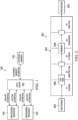
- FIG. 1 is a block diagram of a computer system 100.
- the computer system 100 includes a data cache 102, such as a level one (L1) data cache.
- the data cache 102 stores a subset of the system's data to reduce the time needed to access (e.g., read and/or write) the cached subset. By effectively caching the most commonly used data, the data cache 102 may markedly improve system performance.
- L1 level one
- the data cache 102 may be coupled to one or more processing resources 104 (e.g., processor cores) and to an extended memory 106.
- the extended memory 106 includes other levels of a memory hierarchy, such as an L2 cache, storage devices, etc.
- the data cache 102 may be incorporated into the same die as the processing resource(s) 104 ( e.g ., on-die cache) or may be on a separate die. In either case, the cache 102 is coupled to each processing resource 104 by one or more interfaces used to exchange data between the cache 102 and the processing resource. In this example, the cache 102 is coupled to each processing resource 104 by a scalar interface and a vector interface.
- a command in the event that one interface is busy, a command may be serviced using another interface.
- the associated data may be provided to the processing resource 104 over the vector interface based on interface utilization, data size, and/or other considerations.
- the cache 102 may also be coupled to the extended memory 106 by one or more interfaces. Where more than one interface is present, an interface may be selected based on utilization, data size, and/or other considerations.
- Each interface may have any suitable width.
- the widths of the interfaces may be different from each other, although in many examples, they are integer multiplies of the narrowest interface.
- the scalar interface is 64 bits wide
- the vector interface is 512 bits wide
- the extended memory interface is 1024 bits wide.
- the interfaces may be bidirectional or unidirectional.
- Bidirectional interfaces may include two independent unidirectional interfaces so that data can be transmitted and received concurrently.
- the vector interface includes two 512-bit unidirectional busses, one for receiving data and operations from the processing resource 104, and one for sending data to the processing resource 104.
- the data cache 102 may include a number of pipelines for processing operations received via these interfaces.
- FIG. 2 is a block diagram illustrating a simplified cache memory pipeline 200 for processing a read request. As shown in the cache memory pipeline 200, a processor 202 sends a memory request to a cache memory 204. While the cache memory 204 is described in the context of a L1 cache, the concepts described herein are applicable to any type of cache memory. In certain cases, the memory request may be sent via a cache or memory controller, not shown. In this example, the cache memory pipeline includes five stages, E1, E2, E3, E4, and E5.
- Each cache memory pipeline stage may be allocated a specific number of clock cycles to complete, and in some examples, each stage is allocated one clock cycle such that cached data may be returned to the processor 202 after the E5 memory pipeline stage in five clock cycles.
- a memory request is received by the cache memory 204.
- the memory request includes a memory address of the data to be retrieved from.
- a tag random access memory (RAM) 206 is read to determine what memory addresses are currently store in the cache memory.
- the tag RAM 206 stores a table that records which entries in the memory 208 correspond to which memory addresses in an extended memory.
- the tag RAM may be a bank or portion of memory used to hold the table of memory addresses.
- the cache may be a N-way associative cache where each cache set can hold N lines of memory addresses. As N increases, the number of addresses which are searched through also increases, which in turn increases the amount of time needed to determine whether a requested memory address is in the tag RAM.
- the received memory address is compared to memory addresses stored read from the tag RAM to determine whether there is a cache hit or miss. A cache hit occurs when data associated with a requested memory address is stored in the cache and a cache miss occurs when data associated with the requested memory address is not stored in the cache.
- a portion of the memory 208 associated with the requested memory address is read and at the E5 memory pipeline stage, the requested memory address is provided to the processor 202.
- the memory 208 may be any type of memory suitable for a cache memory, such as dynamic random-access memory (DRAM), static random-access memory (SRAM), registers, etc.
- DRAM dynamic random-access memory
- SRAM static random-access memory
- the pipeline stages illustrate how a memory pipeline can be configured, and as such, omit certain sub-steps and features. In certain implementations, the stages in which certain activities, such as the memory access, are performed may differ.
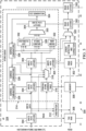
- FIG 3 is a block diagram illustrating a cache pipeline 300 supporting read-modify-write with error-correcting code store queue architecture, in accordance with aspects of this description.
- the pipeline 300 includes a read path (with read path latches 302, tag RAM 306, memory 308, etc.), and write path (write path latches 304, store queue 314, etc.).
- the pipeline 300 includes a tag RAM 306 and a memory 308 (e.g., DRAM or other suitable memory).
- the cache may have any degree of associativity, and in an example, the cache is a direct-mapped cache such that each extended memory address corresponds to exactly one entry in the cache memory 308.
- the cache pipeline 300 may include support for ECC and the memory 308 may be coupled to an error detection and correction circuit 310.
- the memory 308 stores data in blocks along with a set of ECC syndrome bits that correspond to the blocks.
- the memory 308 may provide the stored data block and the corresponding ECC syndrome bits to the error detection and correction circuit 310.
- the error detection and correction circuit 310 may regenerate the ECC syndrome bits based on the data block as read from the memory 208 and compare the regenerated ECC syndrome bits with those that were previously stored. Any discrepancy may indicate that the data block has been read incorrectly, and the ECC syndrome bits may be used to correct the error in the data block. The ability to detect and correct errors makes the cache well-suited to mission critical applications.
- An arbitration unit 312 may be coupled to the memory 308 to arbitrate between conflicting accesses of the memory 308. When multiple operations attempt to access the memory 308 in the same cycle, the arbitration unit 312 may select which operation(s) are permitted to access the memory 308 according to a priority scheme. Many different priority schemes may be used. As an example of a priority scheme, the arbitration prioritizes read operations over write operations because write data that is in the pipeline 300 is available for use by subsequent operations even before it is written to the memory 308, for example via a data forwarding multiplexer 318 of a store queue 314, as will be described in more detail below. Thus, there is minimal performance impact in allowing the write data to wait in the pipeline 300. However, as the pipeline 300 fills with write data that has not yet been written back, the priority of the write operations may increase until they are prioritized over competing read operations.
- the read path may run in parallel with the store queue 314. Because a read operation may refer to data in a write operation that may not have completed yet, the pipeline 300 may include write forwarding functionality that allows the read path to obtain data from the store queue 314 that has not yet been written back to the memory 308.
- the pipeline 300 includes a pending store address table 316 that records the addresses of the operations at each stage of the store queue 314, the data forwarding multiplexer 318 to select data from one of the stages of the store queue 314 for forwarding, and a store queue hit multiplexer 320 that selects between the output of the memory 308 (by way of the error detection and correction circuit 310) and the forwarded store queue 314 data from the data forwarding multiplexer 318.
- stage E1 the cache retrieves a record from the tag RAM 306 that is associated with an address of the read operation to determine whether the data is stored in the cache's memory 308.
- the cache does not need to wait for the tag RAM comparison before requesting data from the memory 308, and thus, the tag RAM comparison between the address of the read operation and the record of cached addresses does not need to extend into a second (E2) or third (E3) cycle.
- the cache may request the data and ECC syndrome bits from the memory 308, if the arbitration unit 312 permits. In this cycle, the cache may also determine whether newer data is available in the store queue 314 by comparing the read address to the pending store address table 316. If so, the data forwarding multiplexer 318 is set to forward the appropriate data from the store queue 314.
- Data and ECC syndrome bits may be provided by the memory 308 in the third cycle in stage E3. However, this data may or may not correspond to the memory address specified by the read operation because the cache may allocate multiple extended memory addresses to the same entry in the cache's memory 308. Accordingly, in the third cycle, the cache determines whether the provided data and ECC from the memory 308 corresponds to the memory address in the read operation (e.g., a cache hit) based on the comparison of the tag RAM record. In the event of a cache hit, the data and ECC bits are received by the error detection and correction circuit 310, which corrects any errors in the data in a fourth cycle in stage E4.
- newer data that has not yet been written to the memory 308 may be present in the store queue 314, and may be forwarded from the store queue 314 by the data forwarding multiplexer 318. If so, the store queue hit multiplexer 320 selects the forwarded data over the corrected data from the memory 308.
- Either the corrected data from the memory 308 or the forwarded data from the store queue 314 is provided to the requesting processor in a fifth cycle in stage E5.
- the example cache may provide data to the processor with full ECC checking and correction in the event of a cache hit in about 5 cycles.
- the pipeline 300 may stall until the data can be retrieved from the extended memory, at which point the data may be written to the memory 308 and the tag RAM 306 may be updated so that subsequent reads of the data hit in the cache.
- the cache may also support a number of operations that read data from the cache and make changes to the data before rewriting it.
- the cache may support read-modify-write (RMW) operations.
- RMW read-modify-write
- a RMW operation reads existing data, modifies at least a portion of the data and overwrites that portion of the data.
- a RMW operation may be performed when writing less than a full bank width. As the write is not for the full bank width, performing an ECC operation on just the portion of the data being written would result in an incorrect ECC syndrome.
- the read functionality of the RWM is used because the portion of the data in the bank that will not be overwritten still contributes to the ECC syndrome bits.
- a RMW operation may be split into a write operation and a read operation, and the pipeline 300 may be structured such that the read operation in the read path stays synchronized with the write operation in the store queue 314. The read operation and the write operation remain synchronized until a read-modify-write merge circuit 322 overwrites at least a portion of the read data with the write data to produce merged data.
- the merged data is provided to an ECC generation circuit 324 that generates new ECC syndrome bits for the merged data, and then the merged data and ECC syndrome bits may be provided to the arbitration unit 312 for storing in the memory 308.
- the read portion of the operation proceeds substantially as described above in stages E1-E4, where the cache compares an address of the read operation to a record of the tag RAM 306, and the cache requests the data and ECC syndrome bits from the memory 308 and/or the store queue 314. Because the RMW operation will modify the data, in examples that track MESI (Modified, Exclusive, Shared, and Invalid) states of entries in the memory 308, a cache hit that is not in either the Modified or Exclusive state may be considered a cache miss. When the data is obtained in the proper state and any errors are corrected, it is provided to the read-modify-write merge circuit 322 in cycle E4 (or later in the event of a cache miss).
- MESI Modified, Exclusive, Shared, and Invalid
- the read-modify-write merge circuit 322 may overwrite at least a portion of the corrected data with the write data to produce merged data.
- the ECC generation circuit 324 generates new ECC syndrome bits for the merged data in stage E5 (or later in the event of a cache miss).
- the merged data and the ECC syndrome bits are provided to the arbitration unit 312 for writing to the cache memory 308.
- sequential RMW operations are received that refer to the same address.
- the store queue 314 may include address comparators 326 for write forwarding that may feed the merged data back to a prior stage of the store queue 314 for use by a subsequent RMW operation. This may be referred to as "piggy-backing."
- the data may be fed back before or after the ECC generation circuit 324.
- the final RMW operation has a complete set of data and ECC syndrome bits. Accordingly, earlier-in-time RMW operations may be canceled before they are written back to the memory 308. This may avoid stalling other operations with writes of obsolete data.
- memory 308 may represent the entirety of the data cache.
- the data cache (which may be an L1 data cache) is associated with a single store queue structure 314.
- the data cache may include 256 rows, with each row having 1024 bits (1Kb) per row.
- the cache may be divided into a plurality of independently addressable banks, and each individual bank may have its own respective store queue structure 314. For instance, consider an embodiment in which the above-mentioned data cache has 256 rows with each row having a line width of 1024 bits, but being divided into 16 banks, with 64 bits per row in a given bank. In such an embodiment, there would be 16 store queues, one for each bank of the data cache. Thus, read and write operations may be sent to the banks in parallel, and each bank arbitrates its own processes in response to the read and/or write operations. By allowing each bank of a multi-bank cache to operate independently, operation of the cache is more efficient since an entire cache line is not locked up when a request is received. Rather, only the portion of the cache line allocated to the bank that received such a request would be locked.
- the cache size described above is only one example and the description is not limited to any particular cache line width, number of banks, or rows, etc.
- vector data may be 512 bits wide.
- a read request to such a multi-bank cache could be performed as 8 parallel reads from 8 banks.
- each cache line within the cache could map to two different addresses in a higher level of memory (e.g., L2 cache or main system memory for instance).
- Line 1 a cache line in a two-way set associate cache and maps to two different addresses in memory, which are referred to as "Address A" and "Address B.”
- a first request is received which is a partial write (e.g., a write to less than a full cache line) and is followed by a read request, like so:
- the Read request is a miss.
- Line 1 may be mapped to either Address A or Address B in this two-way set associative cache, in this instance it is presently mapped to Address A.
- the miss thus occurs because Address B is not found in the tag RAM 306.
- the cache system will service the miss by going to retrieve the data from a higher level of memory, such as an L2 cache and, when the data, which is referred to as "Data 2" in this example is returned, data currently in Line 1 will be evicted in order to store Data 2. This may occur before the earlier Write has completed. In this case, there is no need to complete the Write operation since the Line 1 is going to be evicted anyways. Thus, the Write can be invalidated before its completion, referred to as "inflight.”
- Atomic operations such as an atomic compare and swap
- An atomic compare and swap operation may provide an address, a key value, and a set of new data to be written. The current data at the address is compared to the key, and if they match, the current data at the address is overwritten by the new data.
- the pipeline 300 includes an atomic compare and swap circuit 328 to perform the comparison and forward the new data on for writing if the current data matches the key value.
- the atomic compare and swap circuit 328 may be coupled in parallel with the read-modify-write merge circuit 322 and a function multiplexer 330 may be used to determine which output is provided to the ECC generation circuit 324.
- the read portion of the operation proceeds substantially as described above in stages E1-E4, where the cache compares an address of the read operation to a record of the tag RAM 306 and the cache requests the data and ECC syndrome bits from the memory 308 and/or the store queue 314. Because the atomic compare and swap operation may modify the data, in examples that track MESI states of entries in the memory 308, a cache hit that is not in either the Modified or Exclusive state may be considered a cache miss. When the data is obtained in the proper state, it is provided to the atomic compare and swap circuit 328 in stage E4 (or later in the event of a cache miss).
- the new data and the key may be stored in the write path latches 304.
- the atomic compare and swap circuit 328 may receive the corrected read data, the key, and the new data. If the corrected read data matches the key, the atomic compare and swap circuit 328 provides the new data to the ECC generation circuit 324. The atomic compare and swap circuit 328 may also change the state of the new data to Modified if the read data matches the key.
- the ECC generation circuit 324 generates new ECC syndrome bits for the new data in stage E5 (or later in the event of a cache miss). The new data and the ECC syndrome bits are provided to the arbitration unit 312 for writing to the cache memory 308.
- the pipeline 300 may also perform write forwarding using the address comparators 326 when sequential atomic compare and swap operations are received, similar to that described in the context of the RMW operations.
- FIG. 3 For example, the pipeline 300 may include an arithmetic unit 332 coupled in parallel with the read-modify-write merge circuit 322 and/or the atomic compare and swap circuit 328.
- the arithmetic unit 332 may support any size operands, and in one such example, the arithmetic unit 332 supports addition and subtraction of a 16-bit value from a 64-bit bank.
- Multiplexer 330 may be used to select between the arithmetic unit 332, the read-modify-write merge circuit 322, and the atomic compare and swap circuit 328.
- the read portion of the operation proceeds substantially as described above in stages E1-E4, where the cache compares an address of the read operation to a record of the tag RAM 306 and the cache requests the data and ECC syndrome bits from the memory 308 and/or the store queue 314. Because the histogram operation will modify the data, in examples that track MESI states of entries in the memory 308, a cache hit that is not in either the Modified or Exclusive state may be considered a cache miss. When the data is obtained in the proper state, it is provided to the arithmetic unit 332 in stage E4 (or later in the event of a cache miss).
- the value to be added to the corrected data may be stored in the write path latches 304.
- the arithmetic unit 332 may receive the corrected read data and the value to be added or subtracted from the read data. The arithmetic unit 332 performs the specified addition or subtraction and provides the new data to the ECC generation circuit 324.
- the ECC generation circuit 324 generates new ECC syndrome bits for the new data in stage E5 (or later in the event of a cache miss). The new data and the ECC syndrome bits are provided to the arbitration unit 312 for writing to the cache memory 308.
- the pipeline 300 may also perform write forwarding using the address comparators 326 when sequential histogram operations are received, similar to that described in the context of the RMW operations.
- FIG. 3 illustrates a single pipeline 300 with a single instance of a store queue 314, latches 302 and 304, an error detection and correction circuit 310, etc.
- the memory 308 may be arranged to support more than one independent copy of the pipeline 300. Accordingly, the pipeline 300 may be reproduced multiple times.
- the memory 308 entries are 1024-bit blocks based on the width of the extended memory interface, and the memory 308 is arranged into 16 parallel banks where each 1024-bit block includes 64 bits in each of the 16 banks.
- each of the 16 banks has its own independent pipeline 300.
- a read or write operation from the processor is divided into a number of bank-level operations and each is provided to its respective pipeline 300 so that they may be processed concurrently.
- a 512-bit vector read operation may be divided into eight 64-bit read operations that are provided to eight independent pipelines 300 to be processed in parallel.
- another operation may be received over the scalar interface or a vector interface of another processor and divided into operations that are provided to the remaining pipelines 300.
- the data cache may service multiple independent operations concurrently, with each operation being allocated a subset of the pipelines 300.
- the cache pipeline 300 may be coupled to a victim cache.
- Victim caches may help improve cache miss rates, such as those due to conflict misses.
- a victim cache in certain cases, can have an impact on cache performance similar to increasing the N-way associative number (e.g., a degree of cache associativity). This benefit may be more evident in cases where the victim cache is added to a direct-mapped cache, as a direct mapped cache often has the highest rate of conflict misses. The addition of a victim cache may help improve an overall cache hit rate.
- FIG. 4 is a block diagram illustrating a cache architecture 400 including a victim cache.
- the cache architecture 400 includes a main cache 404 coupled to a victim cache 402, where the victim cache 402 resides after the main cache 404.
- a line of data is evicted out of the main cache 404, rather than moving the line of data to a next level cache (e.g., L2), the line of data is moved to the victim cache 402 and held there until there is a reason to evict it out, such as due to capacity or other reasons.
- the victim cache 402 can service the miss and return the line to the processor 414, reducing the overall latency experienced for a read miss.
- a processor 414 attempts to access address A in the main cache 404 and the victim cache 402, causing a cache miss.
- the main cache 404 may then evict address B from the main cache 404 and create a victim cache (Address B) line in the victim cache 402.
- the read miss of address A then goes out 406 to a higher level memory 412, such as L2 cache, another cache, and/or other memory, to be serviced.
- a higher level memory 412 such as L2 cache, another cache, and/or other memory
- the main cache 404 is checked to see if address B is cached, resulting in a cache miss.
- the victim cache 402 is then checked 408, which returns a hit as address B was stored in the victim cache 402 after being evicted from the main cache 404.
- Address B may then be restored 410 to the main cache 404 and returned as a result to the processor 414.
- the read latency in such a system while faster as compared to having to fetch the address from higher level memory 414 (e.g., L2 cache, main memory, etc.), is still greater than the latency when there is a cache hit in the main cache 404.
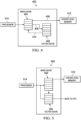
- FIG. 5 is a block diagram illustrating a cache architecture 500 including a parallel victim cache, in accordance with aspects of this description.
- the cache architecture 500 can be thought of as having multiple sub-caches in parallel.
- Each of the main cache 504 and the victim cache 502 has their own independent associativity and the overall cache system 500 may have the appearance of a hybrid way cache system.
- either the main cache 504 or the victim cache 502 may be n-way associative, while the other cache may be fully associative.
- the main cache 504 may be a direct mapped (1-way associative) cache and the victim cache 502 may be fully associative.
- a processor 514 issues a read to address A, which misses in the main cache 504, the miss request goes out to a higher level cache 512 for servicing and the victim line, here address B, is moved to the victim cache 502.
- address B the victim line
- the processor 514 wants to read address B.
- the address of the read is checked against both the main cache 504 and the victim cache 502 in parallel. This results in a read miss in the main cache 504 but a hit in the victim cache 502.
- the read results for address B may then be directly returned from the victim cache 402 to the processor 514.
- both caches are checked in parallel, the read latency remains the same as if the read request was a hit in the main cache 504.
- the overall effect of having a victim cache in parallel to the main cache is that we get the benefit of reducing the cache miss rate while also not impacting the latency in case the subsequent CPU access hits the victim cache.
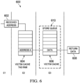
- FIG. 6 is a block diagram illustrating a victim cache memory pipeline 600, in accordance with aspects of this description.
- the victim cache may be a fully associative cache, meaning that there is not a mapping addresses and cache lines. Rather any address may be stored in any cache line of the victim cache.
- the received address is checked, in the E2 stage, against addresses stored in each location in the victim cache tag RAM 604. In certain cases, these locations in the victim cache tag RAM 604 correspond to lines of the victim cache 606. For example, if address A is received at block 602, address A is compared against addresses in the victim cache tag RAM 604 to see if there is a match. If, for example, location 5 of the victim cache tag RAM 604 corresponds to address A, then the data corresponding to address A is stored in address 5 of the victim cache 606. This data is eventually returned to the processor at block 608.
- the victim cache may be desirable for the victim cache to support certain features of the main cache, such as ECC and RMW operations.
- the victim cache may also include a store queue 610 structure to help provide support for RMW and ECC operations, in a manner similar to the store queue 314 as described in conjunction with FIG. 3 .
- caches may include a write-miss buffer.
- a write-miss can occur when a memory write is issued to a cache against a memory address that is not in the cache.
- the memory write may be an atomic operation, the processor that issued the memory write may stall until a memory write complete message is returned to the processor. Rather than stalling the processor until a write to a higher level memory is complete, the cache may store the memory write in a write-miss buffer and returns an indication that the memory write is complete.
- the write-miss buffer this information and then outputs (e.g., drains) the memory write to the target memory address. Once the memory write output to the target memory address is complete, the memory write is removed from the write-miss buffer.
- the write-miss buffer may include three pieces of information for each memory write: the memory address for the write, the corresponding data, and the byte enable (byten) mask for the memory write.
- the byte enable logic or mask that defines a portion of the memory line to be written to.
- write-miss buffers are implemented using dedicated buffer circuitry as a first in first out (FIFO) buffer.
- FIFO write-miss buffers are frequently configured to drain to a higher level memory more or less continuously and do not support features such as write merging.
- a write-miss buffer may be allocated into the cache system using the victim cache.
- FIG. 7 is a block diagram illustrating a victim cache pipeline 700 including a write-miss buffer, in accordance with aspects of this description.
- a write-miss buffer may store the memory address for the write, the data to be written, and the byten logic.
- the memory addresses for a write-miss buffer entry may be stored in a victim cache tag RAM 704 and the corresponding data may be stored in the victim cache RAM 706.
- a byte enable memory 702 may also be added to the victim cache to store the byten logic associated with a write-miss buffer line.
- the MESI RAM 732 may be modified to include an extra bit indicating a line type 708 associated with an entry in the victim cache RAM 706.
- the line type 708 indicates whether a particular line of the victim cache RAM 706 is a cache line or a write-miss buffer line. In certain cases, the line type 708 may be added to another memory, such as the victim cache tag RAM 704, rather than the MESI RAM 718.
- the victim cache system may be configured as a write-miss buffer by adding control logic in read and write-miss state machines to address allocating of write-miss entries inside the victim cache, as well as logic to support handling various address hazards in cases like a read to the same line as a write-miss entry inside the victim cache (selective write-miss flush), and logic to support resolving same address load/stores in datapaths of the victim cache.
- a storage queue 710 structure may also be provided to enable support for RMW and ECC support for write-misses. In certain cases, the storage queue 710 may be used to enable support for RMW and ECC support for write miss operations as well as cache operations.
- the address of the write is checked against memory addresses stored in each location in the victim cache tag RAM 704.
- a write-miss occurs when the address of the write is not found in the victim cache tag RAM 704.
- a determination is made where to store the write-miss in the victim cache. In certain cases, this determination may be made based on entries in the victim cache tag RAM 704. If there is an empty location in the victim cache tag RAM 704, then the address of the write-miss is stored in the victim cache tag RAM 704 in the empty location. If there is not an empty location, then a line may be evicted based on an eviction scheme for allocating the write-miss buffer space.
- the line may have previously been used as a write miss buffer or a cache line.
- the line type 708 corresponding to the location in the victim cache tag RAM 704 of the write-miss may be updated to indicate that the location is being used as a write-miss buffer. For example, a 0 in the line type 708 may indicate the corresponding line is a cache entry, while a 1 in the line type 708 may indicate that the corresponding line is a write-miss buffer entry.
- the line type 708 may be store in another memory location, such as the MESI RAM 732, or in a dedicated memory space, such as a set of registers.
- the data of the write-miss is stored in a line of the victim cache RAM 706 corresponding to the victim cache tag RAM 704 location used.
- the byte enable logic may be stored in a corresponding slot of the byte enable memory 702.
- the byte enable memory 702 may include bits indicating which positions of the byte enable memory 702 are valid.
- the line type bit helps enable storing write miss entries in lines of the victim cache RAM 706 without having to dedicate a portion of the victim cache RAM 706 as a write buffer.
- the victim cache eviction logic for example in an eviction controller 714, may be updated to handle write-miss entries stored in the victim cache to prioritize evicting write-miss entries in favor of store cache entries.
- control logic for read and write state machines of the victim cache controller 734 may be configured to determine that an incoming read request might hit a cache line of the victim cache configured to store a write-miss. In such cases, the victim cache controller 734 may be configured to treat this read hit like a read-miss and evict the stored write miss command to higher level memory and then send the read miss out to the higher level memory.
- cache system are often configured to stall on a miss while a write-miss buffer often does not stall a processor as it buffers the write miss.
- the victim cache controller 734 may be configured to allocate write miss entries to the victim cache without stalling the CPU by speculatively reading an incoming write data so that data can be stored directly in to the victim cache without stalling if it is a write miss.
- the write-misses may stay cached until there is a requirement to evict them out to higher level memories.
- a write-miss stored in the victim cache may stay in the cache system until a defined condition is met, a fence operation is requested, or there are address/hardware conflicts which need a particular write-miss entry to be evicted.
- Maintaining the write-miss buffer until an explicit fence operation is requested may be problematic, for example, if a fence operation is not raised at the end of an operation, and any write-misses stored in the victim cache may be stuck inside the victim cache.
- there can be latency concerns from fence operations as flushing out (e.g., evicting all) write miss buffers stores only in response of a fence operation can result in delays as the cache needs to drain the stored write-misses out to the appropriate memories and then wait for the acknowledgments to return.
- an auto-flushing or draining of write-miss entries stored in the victim cache may be provided. Auto-flushing may be implemented to help drain write-miss entries from the victim cache while reducing the potential latency that may be incurred in the drain process.
- an eviction controller 714 may monitor activity on a processor interface. If the eviction controller 714 detects idle activity on the processor interface, the eviction controller 714 may proceed to start draining write-miss entries from the victim cache. For example, if the eviction controller 714 detects that the processor has not issued any commands for N number of clock cycles, then the eviction controller 714 may internally start an auto-flush process to start draining the stores cached inside victim cache. In certain cases, N may be predetermined. In other cases, N may be configurable. In certain cases, the auto-flush process may walk (e.g., examine in order) the VTag RAM looking for write-miss entries and flushing entries corresponding to write-miss entries. In other cases, the auto-flush process may include logic to flush entries based in a FIFO, least recently used (LRU), random, or other basis.
- LRU least recently used
- the eviction controller 714 may send an eviction trigger request to the victim cache controller 734 for a selected write buffer cache line.
- the victim cache controller 734 checks the store queue to see if there are any entries in the store queue corresponding to a write buffer cache line to be flushed. If there is a corresponding entry in the store queue, then the victim cache controller 734 may wait for the store queue to complete. Once the store queue is emptied, the victim cache controller 734 may evict the selected cache lines.
- the victim cache controller 734 sets up the creation of store miss packets to be sent to higher level caches or other memories.
- These store miss packets may include the corresponding memory address stored in the victim cache tag RAM 704, byte enable logic in the byte enable memory 702, and the data in the victim cache RAM 706.
- the victim cache can then send the store miss packet, for example to a cache controller of a higher level cache or other memory.
- the write miss packet may be sent out to other memories and the corresponding entries in the victim cache RAM 706, victim cache tag RAM 704, and byte enable memory 702 may be invalidated.
- the write miss packet may be placed in a drain buffer 716 temporarily until the write miss packet is accepted (e.g., acknowledged) by the other memory.
- the eviction controller 714 may select a next write miss buffer cache line to evict and proceed to evict the next write miss buffer cache line. If activity is subsequently detected on the processor interface, this auto-flush operation may be cancelled. By doing so, the victim cache is able to utilize idle periods and avoid impacting processor performance when there is activity on the interface by attempting to drain the write-miss buffer entries.
- write-misses stored in the victim cache may be evicted based on a state of the write miss line storing a particular write-miss, rather than a FIFO, LRU, random, or other scheme based on the order which a cache line is allocated.
- the cache is configured to merge data in the cache, cache writes to a memory line from a processor do not imply that the processor needs to read from other portions of the memory line. Further, where a processor has written out a large portion of the memory line, such as half the memory line or the whole memory line, the processor is less likely to need to access (such as merging additional data into) that portion of the memory line again, as compared to where the processor has written only a small portion of the memory line.
- this write miss cache line can be evicted with less potential impact to performance.
- the full, or half full, cache line may be evicted. This helps address the case where a processor is issuing a stream of cache writes-misses which are collectively larger than the victim cache.
- aggressively evicting full or half full write-miss cache lines helps avoid performance issues that may arise when a large number of write-miss items stored in the victim cache are all flushed at once due to a fence operation at the end of an operation.
- the byte enable memory 702 may include two status bits, a half-full line status bit 718 and a full line status bit 720.
- Each line of the byte enable memory 702 corresponds with a cache line in the victim cache ram 206 and each line of the byte enable memory 702 may include the half-full line status bit 718 and the full line status bit 720.
- These status bits may be updated each write cycle where bits are written into a cache line configured as a write miss buffer and the status bits may be calculated based on the bits already stored in the corresponding line of the victim cache RAM 706, as well as the bits that are being written to the victim cache RAM 706 in a write cycle.
- each line of the byte enable memory 702 can include a bit mask indicating which positions (e.g., bytes) of the byte enable memory 702 are valid (e.g., written to). Determining which lines are full or half full can be performed using an XOR over corresponding portions of the bit mask.
- the half-full line status bit 718 may be set when half of a given cache line has been written to, either the least significant bits, or the most significant bits.
- the full line status bit 720 may be set when an entire cache line has been written to.
- the cache lines may then be walked (e.g., examined in order) to determine an address to return that has a full or half full cache line.
- addresses corresponding to full cache lines are selected first and addresses corresponding with half full cache lines are returned if there are no full cache lines. If multiple cache lines are full (or half full, if there are no full cache lines), then the first cache line that is full (or half full) found when walking the cache lines may be selected. If no cache line is full or half full, a write-miss cache line may be selected based on FIFO, LRU, or other logic may be used to determine which cache line to select where there are multiple lines available.
- Evicting write-miss entries may operate similarly to auto-flush except that the store queue is not checked to see if there are any entries corresponding to a full or half full write miss cache line being evicted as this operation is initiated by a read or write miss and is performed after a line has been written to.
- the eviction controller 714 indicates to a victim cache controller 734 to evict the selected cache lines.
- the victim cache controller 734 sets up the creation of store miss packets to be sent to higher level caches or other memories. These store miss packets may include the corresponding memory address stored in the victim cache tag RAM 704, byte enable logic in the byte enable memory 702, and the data in the victim cache RAM 706.
- the store miss packets are sent, for example to a cache controller of a higher level cache or other memory and the corresponding entries in the victim cache RAM 706, victim cache tag RAM 704, and byte enable memory 702 may be invalidated.
- the store miss packet may be placed in a drain buffer 716 temporarily until the store miss packet is accepted (e.g., acknowledged) by the other memory.
- the address of the cache line may be sent to replacement policy logic 722 each write cycle.
- Cache line address which are available may be fed into mux 724 in a replacement address line 726.
- An address generation line 728 may include an address assigned to a received write instruction. If hit/miss logic 730 determines that the address of the received write instruction is a hit, the address is already stored in a line of the victim cache and data from the write instruction is merged to the line. If hit/miss logic 730 determines that the address of the received write instruction is a miss, an address from the replacement address line 728 may be used to write the write-miss command to the victim cache/write miss buffer.
- An eviction process may be triggered if there are no empty cache lines in the victim cache/write miss buffer to allocate the write miss.
- a centralized controller may detect that a write miss has been received that needs to be stored into the victim cache. The centralized controller may instruct the victim cache controller 734 to ensure that there is a cache line available. This cache line may be based on a location provided by either the replacement address 726, or the address generation 728. If there is already a write miss stored in the identified location, the write miss may be evicted.
- FIG. 8 is a block diagram of a MESI RAM 800, in accordance with aspects of this description.
- the MESI RAM 800 may be a memory (e.g., SRAM) or set of registers (e.g., register file), used to track the MESI status of a corresponding cache line.
- the victim cache in certain cases, may track MESI states in MESI state bits 802 in the MESI RAM 800 for cache entries as a part of writing data.
- the MESI RAM 800 includes a line corresponding to each line of the corresponding cache, here, the victim cache.
- the main cache may include a corresponding MESI RAM.
- a single MESI RAM may be shared by both a main and victim cache.
- the MESI RAM 800 may have a set of bits for tracking the MESI state of each cache line stored in the victim cache. In certain cases, the MESI RAM 800 may be expanded with additional bits to track other states of cache lines in the victim cache. The MESI RAM 800 may be expanded to track additional states by including additional columns for the additional states. In this example, the MESI RAM has been expanded to include state bits in a bit field to track a privilege level 804 for each cache line, a red tag 806, a blue tag 808, whether a line is valid 810, and whether a line is a write miss buffer or victim cache line 812. It may be noted that while shown as a part of the MESI RAM, the state bits may be placed within other memories in other embodiments, such as the tag RAM 704, or in a separate memory altogether. The MESI RAM may be configured to track additional states not shown here.
- entries in the write-miss buffer may be associated with a "color" tag.
- This color tag may be represented by one or more bits such that when a bit is set for a write-miss buffer entry, the color associated with the write-miss buffer entry may be "blue" and when the bit is not set, or another bit is set, the write-miss buffer entry may be "red.”
- Tagging helps allow certain write-miss buffer entries to be associated with a particular process running on a processor, while other write-miss buffer entries may be associated with another process running on the processor.
- a processor may want to flush all write-miss buffer entries associated with a particular process (e.g., a selective fence operation), but not the write-miss buffer entries associated with another process.
- a processor may assert a drain signal. Along with the asserted drain signal, the processor may provide an indication that a particular tag should be prioritized for draining, either the red or blue tag. Referring back to FIG. 7 , the drain signal is passed to the eviction controller 714.
- the eviction controller 714 may check an availability of a higher level cache or memory to see whether the higher level cache or memory is busy. If the higher level cache or memory is unavailable, the eviction controller 714 may stall the processor. If the higher level cache or memory is available, then the eviction controller 714 may send an eviction trigger request indicating the prioritized tag to the victim cache controller 734.
- the victim cache controller 734 may then check with the store queue to see if there are any outstanding entries in the store queue for any bank of the victim cache RAM 706.
- the victim cache controller 734 may also indicate to the store queue 710 to escalate the priority of draining the store queue. If there is data, for example in the store queue, that has not yet been stored to the victim cache, the eviction controller 714 may wait for the store queue 710 to complete. Once the store queue 710 is emptied, the eviction controller 714 indicates to a victim cache controller to evict the selected cache lines.
- the victim cache controller 734 sets up the creation of store miss packets to be sent to higher level caches or other memories.
- These store miss packets may include the corresponding memory address stored in the victim cache tag RAM 704, byte enable logic in the byte enable memory 702, and the data in the victim cache RAM 706.
- the victim cache can then send the store miss packet, for example to a cache controller of a higher level cache or other memory.
- the write miss packet may be sent out to other memories and the corresponding entries in the victim cache RAM 706, victim cache tag RAM 704, and byte enable memory 702 may be invalidated.
- the write miss packet may be placed in a drain buffer 716 temporarily until the write miss packet is accepted (e.g., acknowledged) by the other memory. This flushing continues until the processor ceases to assert the drain signal.
- draining of the write-miss buffer stops wherever in the draining process the victim cache is in when the drain signal stops being asserted. Once all write miss buffer entries of the indicated color tag have been drained, an idle signal is asserted back to the processor. If the processor continues to assert the drain signal, other write miss buffer entries associated with the other color tag may be drained.
- write-misses in a cache system helps provide an opportunity to merge additional write misses to the write miss already in the cache system. As write-misses can stay longer inside the cache, the cache has an opportunity to merge any future write-misses to write-misses already existing in the cache system, thus reducing the write-miss traffic out to higher level memories. Reducing the write-misses being sent to higher level memories can reduce the pressure on those memories and help improve overall performance.
- a write merge may occur when a processor issues a second store or write command to a particular address at block 712.
- the address of the second write may be checked, by the hit/miss logic 730, against a set of memory addresses stored in each location in the victim cache tag RAM 704.
- a replacement policy 722 logic determines a location inside of the victim cache where the write transaction could be allocated in case of a write miss.
- the write miss is allocated an entire cache line, even if the data in the write miss does not need an entire cache line.
- a set of memory addresses may be associated with each write miss stored in the victim cache, including the memory address in the write miss, along with a set of memory addresses either before, after, or both before and after the memory address in the write miss. If the address of the second write is determined to be within a set of memory addresses associated with a write-miss stored in the victim cache, then a cache hit is detected and the hit/miss logic returns the location in the victim cache where the write-miss is currently stored.
- the color type and privilege level associated with the second write is merged, for example by the victim cache controller 734, with the currently stored color type and privilege level and the MESI RAM 732 is updated. In certain cases, merging the privilege level may be performed with reference to a privilege merge table 736.
- the data of the second write is also merged into the corresponding line of the victim cache RAM 706 and the corresponding entry of the byte enable memory 702 updated based on the byte enable logic associated with the second write, for example by the victim cache controller 734.
- the store queue 710 may also include write merge functionality. For example, when back to back writes are issued to the same address, the store queue 710 may internally merge them to help minimize a number of writes to issue to the victim cache RAM 706.
- write merging may be performed across privilege levels. Merging the privilege level may be performed when performing write merging. For example, a first write-miss stored in the victim cache may be associated with a first privilege level. A second write associated with a second privilege level may be merged with the stored first write-miss. To perform the merge, the privilege levels should be merged as well. In certain cases, the privilege levels may be merged by merging the privilege levels to the lower level of the privilege levels. For example, in an embodiment, a write operation may be associated with a two part privilege level such as root/guest-user/supervisor. A first write-miss may be received with a privilege level of root-user. This first write-miss may be written to the write miss buffer in the victim cache.
- a second write with privilege level of guest-supervisor may be received, the second write directed to an address within the set of addresses associated with the first write-miss.
- the lower privilege level may be used, resulting in a merged privilege level of guest-user.
- merging the privilege levels may operate in the same way when merging is performed for multiple datapaths.
- privilege level merging may be encoded in the privilege merge table 736, indicating how different privilege levels may be merged.
- the privilege merge table 736 may be predefined. An example of a predefined privilege merge table 736 is shown in Table 1.
- the privilege merge table 736 may be configurable.
- write merging may be performed for color tags.
- a first write-miss stored in the victim cache may be associated with a first color tag, such as red.
- the first write-miss may be associated with an entry in the MESI RAM 800 with a bit set in the red tag 806 of a bit field.
- a second write associated with a second color tag may be merged with the stored first write-miss.
- the color tags should be merged as well.
- the color tags may be merged by combining the color tags of the writes. For example, if both writes are red tagged, then the merged write remains red tagged. Similarly, the merged write would be blue tagged if both writes are blue tagged.
- the merged write is tagged both red and blue.
- the merged write may have a bit set in the red tag 806 of the bit field and a bit set in the blue tag 808 of the bit field.
- a drain operation is then performed, for example for blue tags, the merged write would be drained.
- red tags the merged write would also be drained as the merged write is tagged as both red and blue.
- FIG. 9 is an architectural block diagram of a cache system 900 including a write-miss buffer, in accordance with aspects of this description.
- a cache 902 may receive cache requests from a processor 904 via a processor interface 906.
- the cache 902 may be configured to handle either scalar or vector data, or both.
- the cache 902 is logically divided into parallel sub-caches including a main cache 908 and a victim cache 910. While a single main cache 908 and victim cache 910 are shown, certain embodiments can include multiple main caches 908 and victim caches 910 pairs. In certain cases, there may be a different number of main caches 908 and victim caches 910.
- a main cache tag RAM access controller 912 accesses and checks a main cache tag RAM 914 against memory addresses included in the cache requests to determine whether a memory address is stored in the main cache 908.
- a main cache controller 916 directs the appropriate allocation, eviction, arbitration, merge, etc. processes and reads/writes into the main cache memory 918.
- a main cache store queue structure 920 as described in conjunction with FIG. 3 , provides features such as RMW, ECC, write merging, etc.
- the overall architecture of the victim cache 910 is similar to that of main cache 908.
- a victim cache tag RAM access controller 922 accesses and checks a victim cache tag RAM 924 against memory addresses included in the cache requests to determine whether a memory address is stored in the victim cache 910.
- a victim cache controller 926 similarly directs the appropriate allocation, eviction, arbitration, merge, etc. processes and reads/writes into the victim cache memory 928.
- a victim cache store queue 930 provides RMW, ECC, and other features, as described in conjunction with FIG. 3 .
- Victim cache logic 932 helps coordinate operations as between the victim cache 910 and the main cache 908.
- the victim cache logic 932 is shown separately, the victim cache logic 932 may be integrated with or a part of other elements, such as the victim cache controller 926.
- the victim cache 908 includes certain elements which help enable the victim cache 908 to support write-miss buffer functionality.
- auto flush logic 934 may monitor the processor interface 906 and direct draining the portions of the victim cache memory 928 allocated for write-miss buffering, for example, to higher level caches and memories via one or more memory interfaces 936.
- MESI RAM 938 or the victim cache tag RAM may be configured to include one or more bit fields to store state information regarding write-miss buffer entries stored in the victim cache 910.
- the victim cache and main cache may include multiple datapaths while configured as parallel caches which appear as a single cache to a processor.
- Each datapath is configured to handle a particular command in parallel with the other datapaths.
- a first datapath 910 may be handling a read command to the main cache while the second datapath 942 handles a write-miss to the victim cache.
- each command combination could result in a cache hit/hit, hit/miss, miss/hit, or miss/miss.
- a centralized controller 944 may help coordinate handling of read and write requests as between the main cache 908 and the victim cache 910.
- the centralized controller 944 may be configured to handle coordination as between the main cache 908 and the victim cache 910 and handing off tasks for the main cache 908 and the victim cache 910 to the main cache controller 916 and victim cache controller 926, respectively.
- the centralized controller 944 may also detect and handle potential conflicts as well.
- the centralized controller 944 may check with the main cache 908 and the victim cache 910 to determine that the addressed memory location of the read request is not stored in either the main cache 908 nor the victim cache 910 and thus is a read miss.
- the centralized controller 944 may also check the victim cache 910 to determine that the addressed memory location is not stored as a write-miss in the victim cache 910, or is being flushed out of the victim cache 910. If the addressed memory location is stored as a write-miss in the victim cache 910, then the centralized controller 944 may stall the read request to flush the addressed memory location.
- the centralized controller 944 may then issue a request to a higher level cache or memory for the addressed memory location.
- a read or a write request is a hit in the main cache 908, the results of the victim cache 910 may be disregarded.
- main cache 908 is configured as a one way associative cache
- cache request conflicts as with multiple datapaths are straight forward.
- Cache request conflicts from the multiple datapaths may be an issue for in the victim cache 910 where the victim cache 910 is fully associative and can store write-miss entries as well as cache entries.
- Cache request conflicts for two datapaths may be handled as described in the following examples.
- cache operations are described in the context of a particular datapath. However, the examples are directed to combinations of particular cache operations, and which datapath a particular cache operation is on does not matter.
- cache read miss for the first datapath and a cache write hit for the second datapath, with two different memory addresses.
- cache requests can go to any location within the victim cache 910.
- address generation 728 for a location within the victim cache occurs in the E2 pipestage along with address lookup in the victim cache tag RAM 704, thus address generation 728 for a location within the victim cache is performed before it is known whether an address of the cache request is a hit or miss.
- centralized controller 944 determines that there is a read miss on the main cache 908, a request to obtain the memory address of the read request is issued to a higher level cache or memory.
- the memory address of the read request of the first datapath maps to a single location in the main cache 908. If there is already cached data in the single location, the already cached data is evicted from the main cache 908 to the victim cache 910 to the pre-generated location within the victim cache 910. If this pre-generated location is the same location the cache write of the second datapath is a hit on, a conflict occurs. This conflict may be detected by the centralized controller 944.
- address generation for a location within the victim cache 910 occurs before it is known whether the address of cache request is a hit or a miss, thus there is an address generated for a second location within the victim cache 910 for the cache write of the second datapath before the determination that the cache write is a hit. Based on the detection of the conflict, this second location within the victim cache may be used to store the data evicted from the main cache 908 by the read miss.
- the main cache is a one-way associate cache (e.g., direct mapped cache) where particular memory addresses are mapped to particular locations within the main cache.
- direct mapped cache the cache read and the cache write are mapped to the same location in the main cache.
- a request to obtain the memory address of the read request is issued to a higher level cache or memory and the already cached data is evicted from the main cache 908 to the victim cache 910 to a pre-generated location, here location A, within the victim cache 910.
- the cache write of the second datapath hits the same location in the main cache which is being evicted.
- One possible solution to such a conflict is to load the requested read miss from the higher level cache or memory directly to the victim cache in a separate location.
- Another solution to the conflict is for the centralized controller 944 to stall the read miss such that the already cached data is not evicted to the victim cache 910 until after the cache write of the second datapath completes to location A in the main cache and location A is then evicted to the victim cache. In certain cases, the stall may occur while waiting for the memory write and eviction to complete.
- a first cache write may be received on the first datapath for the victim cache 910 and a second cache write is also received on the second datapath for the victim cache 910. If the first cache write and the second cache write are addressed to different memory addresses, then both cache writes may proceed in parallel to the victim cache 910. If the first cache write and the second cache write are both addressed to the same memory address and both are cache misses, then the victim cache controller 926 allocates a single location in the victim cache write-miss memory 928 and merges the first cache write and the second cache write in the victim cache store queue 930. The merged data may then be written to the victim cache write-miss memory 928 along with merged byte enable, privilege, and color tag information. If the first cache write and the second cache write are both addressed to the same memory address and both are cache hits, both the first cache write and the second cache write are merged into the cache at the hit location.
- a cache read may be received on the first datapath for the victim cache 910 and a cache write may be received on the second datapath for the victim cache 910.
- the cache read and cache write proceed in parallel without conflicts.
- the cache read and cache write also proceed in parallel without conflicts.
- the cache read may use an address generated for a location within the victim cache 910 for the cache write as described above.
- both the cache read and the cache write use addresses generated for locations within the victim cache 910.
- a cache read may be received on the first datapath for the main cache 908 and a cache write may be received on the second datapath for the main cache 908.
- the cache read may be a hit for a location (e.g., cache line or slot) of the main cache 908.
- the cache write may also be a hit for the same location of the main cache 908.
- the cache read and the cache write may proceed in parallel without conflicts as the cache read may be performed relatively quickly and conclude before the cache write needs to access main cache location as the cache write proceeds through the store queue.
- the cache read may be a hit for a location in the main cache 908.
- the cache write may be a miss for the same location in the main cache 908.
- the cache commands proceed in parallel normally as the cache read may complete before the cache write needing to access the cache location.
- the cache read may be a miss for a location in the main cache 908.
- the cache write may be a hit for the same location in the main cache 910.
- the cache read may be stalled until after the cache write of the second datapath completes to the location in the main cache 908 and is evicted to the victim cache 908.
- the cache read then proceeds to read the set of addresses from the higher level cache or memory into the main cache 910.
- the cache read may be a miss for a first location in the main cache 908.
- the cache write may also be a miss for the same location in the main cache 908. In such a case, the cache read and the cache write may proceed in parallel without conflicts.
- a cache read may be received on the first datapath for the victim cache 910 and a cache write may be received on the second datapath for the victim cache 910.
- the cache read may be a hit for an address stored in the victim cache 910.
- the cache write may also be a hit for the same address stored in the victim cache 910.
- the cache read may proceed first and the cache write may be stalled until after the cache read completes.
- the order of the cache write and cache read may be based on the datapath on which the cache write and cache read are received, with the cache command arriving on a lower (or higher) numbered datapath being completed before the other cache command.
- the cache read may be a miss for an address stored in the victim cache 910.
- the cache write may also be a miss for the same address stored in the victim cache 910.
- the cache write command may be forwarded to a higher level cache or memory and then the cache read may obtain the data from the higher level cache or memory after the cache write command completes for storage into the victim cache 910.
- a first cache read may be received on the first datapath for the victim cache 910 and a second cache read may be received on the second datapath for the victim cache 910. If the first cache read and the second cache read are for different memory addresses, then there are no conflicts for either hits or misses.
- the first cache read may be a miss for a first address of a set of addresses.
- the second cache read may also be a miss for a second address of the same set of addresses. If the first cache read and the second cache read have different priority levels, a higher level cache or memory is accessed based on the higher of the different priority levels. Otherwise, the higher level cache or memory is accessed and the set of memory addresses obtained for storage in the victim cache 910. The case where the first cache read and the second cache read are for the same address is handled identically.
- FIG. 10 is a flow diagram illustrating a technique for caching data 1000, in accordance with aspects of this description.
- a caching system receives a write memory request for a memory address.
- a caching system such as a L1 cache
- a first sub-cache of the caching system determines that the memory address is not cached in the first sub-cache.
- the caching system may include two parallel caches, a main cache and a victim cache. Memory addresses of cache requests may be checked as against both the main cache and victim cache in parallel.
- a write-miss occurs when a write request is received for a memory address not contained within the caching system.
- second sub-cache of the caching system determines that the memory address is not cached in the second sub-cache.
- data associated with the write memory request is stored in the second sub-cache.
- the data of the write memory request may be stored in the victim cache.
- the address associated with the write memory request may be stored in a tag RAM of the victim cache and byte enable logic associated with the write memory request may be stored in a byte enable memory of the victim cache.
- an indication that the stored data corresponds to a write-miss is stored in a line type bit of the second sub-cache.
- the victim cache includes a line type bit associated with lines of the victim cache.
- a bit may be set in the line type bit indicating that a particular line of the victim cache includes a write-miss.
- the stored data may be flushed based on the indication. For example, stored write-miss data may be flushed the victim cache to a higher level memory by checking the line type bits of the cache lines and flushing the lines associated with write-misses.
- FIG. 11 is a flow diagram illustrating a technique for caching data 1100, in accordance with aspects of this description.
- a caching system receives a write memory request for a memory address.
- a caching system such as a L1 cache
- a first sub-cache of the caching system determines that the memory address is not cached in the first sub-cache.
- the caching system may include two parallel caches, a main cache and a victim cache. Memory addresses of cache requests may be checked as against both the main cache and victim cache in parallel.
- a write-miss occurs when a write request is received for a memory address not contained within the caching system.
- second sub-cache of the caching system determines that the memory address is not cached in the second sub-cache.
- data associated with the write memory request is stored in the second sub-cache.
- the data of the write memory request may be stored in the victim cache.
- the address associated with the write memory request may be stored in a tag RAM of the victim cache and byte enable logic associated with the write memory request may be stored in a byte enable memory of the victim cache.
- an indication that the stored data corresponds to a write-miss is stored in a line type bit of the second sub-cache.
- the victim cache includes a line type bit associated with lines of the victim cache.
- a bit may be set in the line type bit indicating that a particular line of the victim cache includes a write-miss.
- a line of the second sub-cache storing the write-miss is evicted based on an indication that the line has been fully written. For example, a bit may be calculated based on the byte enable logic indicating whether all, or half, of the bytes of a cache line have been filled with write data. Cache lines which are filled, or half filled, may be evicted from the victim cache based on the bit.
- FIG. 12 is a flow diagram illustrating a technique for caching data 1200, in accordance with aspects of this description.
- a caching system receiving a write memory command for a memory address, the write memory command associated with a first privilege level.
- a caching system such as a L1 cache, can receive, via a processor interface, a write request from a processor.
- a first sub-cache of the caching system determines that the memory address is not cached in the first sub-cache.
- the caching system may include two parallel caches, a main cache and a victim cache. Memory addresses of cache requests may be checked as against both the main cache and victim cache in parallel.
- a write-miss occurs when a write request is received for a memory address not contained within the main cache nor the victim cache.
- a second sub-cache of the caching system determines that the memory address is not cached in the second sub-cache, and the second sub-cache is configured to store, in parallel with the first sub-cache, cache data evicted from the first sub-cache and write-memory commands that are not cached in the first sub-cache.
- data associated with the write memory command is stored in the second sub-cache.
- a color tag bit associated with the data is stored in the second sub-cache.
- a color tag bit may be stored within a bit field of a memory of the second sub-cache, such as the MESI RAM.
- the stored data is evicted based on the color tag bit. For example, cache lines storing write miss data associated with a particular color tag bit may be evicted while the processor is asserting a drain signal and a color tag priority indication. After all cache lines with the particular color tag bit have been drained, the caching system may assert an idle signal. If the processor continues to assert the drain signal, other cache lines storing write miss data associated with other color tags may also be evicted.
- FIG. 13 is a flow diagram illustrating a technique for caching data 1300, in accordance with aspects of this description.
- a caching system receives a write memory command for a memory address, the write memory command associated with a first color tag.
- a caching system such as a L1 cache, can receive, via a processor interface, a write request from a processor. The write request may include in an indication of a color tag associated with the write request.
- a first sub-cache of the caching system determines that the memory address is not cached in the first sub-cache.
- the caching system may include two parallel caches, a main cache and a victim cache.
- Memory addresses of cache requests may be checked as against both the main cache and victim cache in parallel.
- a write-miss occurs when a write request is received for a memory address not contained within the caching system.
- second sub-cache of the caching system determines that the memory address is not cached in the second sub-cache.
- data associated with the write memory command is stored in a cache line of the second sub-cache.
- the data of the write request may be stored in a cache line of the victim cache.
- the address associated with the write memory request may be stored in a tag RAM of the victim cache and byte enable logic associated with the write memory request may be stored in a byte enable memory of the victim cache.
- the first color tag is stored in the second sub-cache.
- the color tag may be stored using two bits within a bit field of a memory of the second sub-cache, such as the MESI RAM.
- a second write memory command for the cache line is received, the write memory command associated with a second color tag.
- a second write request to a memory address targeting the same cache line as the first write request may be received.
- the second write request is associated with a second color tag.
- the second color tag may be the same or different from the first color tag.
- the second color tag is merged with the first color tag. For example, where the first color tag and the second color tag represent the same color, merging the two tags continues to set that color tag. Where the two color tags are different, merging may set both color tags.
- the merged color tag is stored.
- the cache line may be evicted based on the merged color tag. For example, where the first color tag and the second color tag represent the same color, eviction may be based on that color tag. Where the two color tags are different, eviction may be based on either color tag.
- FIG. 14 is a flow diagram illustrating a technique for caching data 1400, in accordance with aspects of this description.
- a caching system receiving a first write memory command for a memory address, the first write memory command associated with a first privilege level.
- a caching system such as a L1 cache, can receive, via a processor interface, a write request from a processor.
- a first sub-cache of the caching system determines that the memory address is not cached in the first sub-cache.
- the caching system may include two parallel caches, a main cache and a victim cache. Memory addresses of cache requests may be checked as against both the main cache and victim cache in parallel.
- a write-miss occurs when a write request is received for a memory address not contained within the main cache nor the victim cache.
- a second sub-cache of the caching system determines that the memory address is not cached in the second sub-cache, and the second sub-cache is configured to store, in parallel with the first sub-cache, cache data evicted from the first sub-cache and write-memory commands that are not cached in the first sub-cache.
- first data associated with the first write memory command is stored in a cache line of the second sub-cache.
- the first privilege level is stored in the second sub-cache.
- the first privilege level may comprise a two part privilege level, such as root/guest-user/supervisor.
- This two part privilege level may be stored using two bits within a bit field of a memory of the second sub-cache, such as the MESI RAM.
- a second write memory command for the cache line is received, the second write memory command associated with a second level of privilege.
- a second write request to a memory address targeting the same cache line as the first write request may be received.
- the second write request is associated with a second privilege level, which may be the same or different from the first write request.
- the first level of privilege with the second level of privilege are merged.
- the privilege levels may be merged based on a privilege merge table or may be merged by selecting the lower privilege level of the privilege levels being merged.
- the merged privilege level are stored.
- the merged privilege level is output with the cache line.
- the cache line including a merged first write request and second write request may be evicted in a store miss packet including the merged privilege level to a higher level cache or memory.
- FIG. 15 is a flow diagram illustrating a technique for caching data 1500, in accordance with aspects of this description.
- a caching system receives a write memory request for a memory address.
- a caching system such as a L1 cache
- a first sub-cache of the caching system determines that the memory address is not cached in the first sub-cache.
- the caching system may include two parallel caches, a main cache and a victim cache. Memory addresses of cache requests may be checked as against both the main cache and victim cache in parallel.
- a write-miss occurs when a write request is received for a memory address not contained within the caching system.
- second sub-cache of the caching system determines that the memory address is not cached in the second sub-cache.
- data associated with the write memory request is stored in the second sub-cache.
- the data of the write memory request may be stored in the victim cache.
- the address associated with the write memory request may be stored in a tag RAM of the victim cache and byte enable logic associated with the write memory request may be stored in a byte enable memory of the victim cache.
- an indication that the stored data corresponds to a write-miss is stored in a line type bit of the second sub-cache.
- the victim cache includes a line type bit associated with lines of the victim cache. A bit may be set in the line type bit indicating that a particular line of the victim cache includes a write-miss.
- FIG. 16 is a flow diagram illustrating a technique for caching data 1600, in accordance with aspects of this description.
- a caching system receives two or more cache commands.
- a caching system such as a L1 cache
- a conflict is determined to exist between the two or more cache commands.
- a cache controller may determine that a cache conflict exists as between the two cache commands.
- a conflict can arise when the two cache commands cause conflicting changes to the same cache location.
- a conflict resolution is determined between the received two or more cache commands.
- two or more cache commands are sent to a first sub-cache and a second sub-cache, and the second sub-cache is configured to store, in parallel with the first sub-cache, cache data evicted from the first sub-cache and write-memory commands that are not cached in the first sub-cache.
- Couple is used throughout the specification. The term may cover connections, communications, or signal paths that enable a functional relationship consistent with the description of this description. For example, if device A generates a signal to control device B to perform an action, in a first example device A is coupled to device B, or in a second example device A is coupled to device B through intervening component C if intervening component C does not substantially alter the functional relationship between device A and device B such that device B is controlled by device A via the control signal generated by device A.
Landscapes
- Engineering & Computer Science (AREA)
- Theoretical Computer Science (AREA)
- General Physics & Mathematics (AREA)
- Physics & Mathematics (AREA)
- General Engineering & Computer Science (AREA)
- Software Systems (AREA)
- Computer Hardware Design (AREA)
- Quality & Reliability (AREA)
- Computational Mathematics (AREA)
- Mathematical Analysis (AREA)
- Mathematical Optimization (AREA)
- Pure & Applied Mathematics (AREA)
- Multimedia (AREA)
- Computing Systems (AREA)
- Memory System Of A Hierarchy Structure (AREA)
Claims (15)
- Système de mise en cache comprenant :un premier sous-cache ; etun second sous-cache (700) en parallèle au premier sous-cache, dans lequel le second sous-cache (700) inclut :un ensemble de lignes de cache ;des bits de type de ligne (708) configurés pour stocker une indication du fait qu'une ligne de cache correspondante de l'ensemble de lignes de cache est configurée pour stocker des données d'échec en écriture ; etun contrôleur d'éviction (714) configuré pour évacuer des données d'échec en écriture stockées sur la base des bits de type de ligne (708).
- Système de mise en cache selon la revendication 1, dans lequel le second sous-cache (700) comprend en outreune mémoire vive d'étiquette(s), RAM, (206, 306, 604, 704, 914, 924) configurée pour stocker une adresse de mémoire associée aux données d'échec en écriture stockées ; etune mémoire de validation d'octet(s) (702) configurée pour stocker une logique de validation d'octet(s) associée aux données d'échec en écriture stockées, etdans lequel le contrôleur d'éviction (714) est configuré pour évacuer les données d'échec en écriture stockées en transmettant une requête d'écriture en mémoire à une mémoire de niveau plus élevé (412, 414) sur la base de l'adresse de mémoire stockée et de la logique de validation d'octet(s) stockée.
- Système de mise en cache selon la revendication 1, dans lequel le système de mise en cache inclut en outre une interface de processeur (906), et dans lequel le contrôleur d'éviction (714) est en outre configuré pour :surveiller l'activité sur l'interface de processeur (906) ; etévacuer les données d'échec en écriture stockées sur la base de l'activité surveillée.
- Système de mise en cache selon la revendication 3, dans lequel la surveillance de l'activité sur l'interface de processeur (906) comprend la détection d'une activité en mode inactif sur l'interface de processeur (906).
- Système de mise en cache selon la revendication 4, dans lequel la détection de l'activité en mode inactif comprend la détermination de si des requêtes de mémoire ont été ou non reçues pendant un nombre prédéterminé de cycles d'horloge.
- Système de mise en cache selon la revendication 4, dans lequel le contrôleur d'éviction (714) est en outre configuré pour :déterminer que l'activité sur l'interface de processeur (906) a repris ; etannuler l'évacuation des données d'échec en écriture stockées.
- Système de mise en cache selon la revendication 6, dans lequel la détermination du fait que l'activité sur l'interface de processeur (906) a repris comprend la détection d'une réception de requête de cache en provenance du processeur (202, 414, 514, 904).
- Dispositif comprenant :un processeur (202, 414, 514, 904) ; etun système de mise en cache selon l'une quelconque des revendications 1 à 7.
- Procédé pour mettre en cache des données, comprenantla réception, par un système de mise en cache, d'une requête de mémoire en écriture pour une adresse de mémoire ;la détermination, par un premier sous-cache du système de mise en cache, du fait que l'adresse de mémoire n'est pas mise en cache dans le premier sous-cache ;la détermination, par un second sous-cache (700) du système de mise en cache, du fait que l'adresse de mémoire n'est pas mise en cache dans le second sous-cache (700) ;le stockage de données associées à la requête de mémoire en écriture dans le second sous-cache (700) ;le stockage, dans un bit de type de ligne du second sous-cache (700), d'une indication du fait que les données stockées correspondent à un échec en écriture ; etl'évacuation des données stockées sur la base de l'indication.
- Procédé selon la revendication 9, dans lequel l'évacuation des données stockées comprend la transmission, par le second sous-cache (700), d'une requête d'écriture en mémoire sur une mémoire de niveau plus élevé.
- Procédé selon la revendication 9, comprenant en outre la surveillance de l'activité sur une interface de processeur (906) et dans lequel l'évacuation des données stockées est en outre basée sur l'activité surveillée.
- Procédé selon la revendication 11, dans lequel la surveillance de l'activité sur l'interface de processeur (906) comprend la détection d'une activité en mode inactif sur l'interface de processeur (906).
- Procédé selon la revendication 12, dans lequel la détection de l'activité en mode inactif comprend la détermination du fait que des requêtes de mémoire n'ont pas été reçues pendant un nombre prédéterminé de cycles d'horloge.
- Procédé selon la revendication 12, comprenant en outre :la détermination du fait que l'activité sur l'interface de processeur (906) a repris ; etl'annulation de l'évacuation des données d'échec en écriture stockées.
- Procédé selon la revendication 14, dans lequel la détermination du fait que l'activité sur l'interface de processeur (906) a repris comprend la détection d'une réception de requête de cache.
Priority Applications (1)
| Application Number | Priority Date | Filing Date | Title |
|---|---|---|---|
| EP24190664.3A EP4443435A3 (fr) | 2019-05-24 | 2020-05-26 | Cache victime prenant en charge des entrees ecriture de justesse de vidage |
Applications Claiming Priority (3)
| Application Number | Priority Date | Filing Date | Title |
|---|---|---|---|
| US201962852494P | 2019-05-24 | 2019-05-24 | |
| US16/882,369 US11194729B2 (en) | 2019-05-24 | 2020-05-22 | Victim cache that supports draining write-miss entries |
| PCT/US2020/034557 WO2020243095A1 (fr) | 2019-05-24 | 2020-05-26 | Cache victime prenant en charge des entrées écriture de justesse de vidage |
Related Child Applications (2)
| Application Number | Title | Priority Date | Filing Date |
|---|---|---|---|
| EP24190664.3A Division EP4443435A3 (fr) | 2019-05-24 | 2020-05-26 | Cache victime prenant en charge des entrees ecriture de justesse de vidage |
| EP24190664.3A Division-Into EP4443435A3 (fr) | 2019-05-24 | 2020-05-26 | Cache victime prenant en charge des entrees ecriture de justesse de vidage |
Publications (3)
| Publication Number | Publication Date |
|---|---|
| EP3977295A1 EP3977295A1 (fr) | 2022-04-06 |
| EP3977295A4 EP3977295A4 (fr) | 2022-08-03 |
| EP3977295B1 true EP3977295B1 (fr) | 2024-09-04 |
Family
ID=73456693
Family Applications (6)
| Application Number | Title | Priority Date | Filing Date |
|---|---|---|---|
| EP20815004.5A Active EP3977296B1 (fr) | 2019-05-24 | 2020-05-26 | Procédés et appareil permettant de faciliter la mise en cache d'échec d'écriture dans un système de mémoire cache |
| EP24190664.3A Pending EP4443435A3 (fr) | 2019-05-24 | 2020-05-26 | Cache victime prenant en charge des entrees ecriture de justesse de vidage |
| EP25193762.9A Pending EP4636601A3 (fr) | 2019-05-24 | 2020-05-26 | Procédés et appareil pour faciliter une mise en cache de non-récupération d'écriture dans un système de mémoire cache |
| EP20813951.9A Active EP3977299B1 (fr) | 2019-05-24 | 2020-05-26 | Procédé et appareil destinés à faciliter un support de lecture-modification-écriture en pipeline dans une mémoire cache |
| EP20812543.5A Active EP3977295B1 (fr) | 2019-05-24 | 2020-05-26 | Cache victime prenant en charge des entrées écriture de justesse de vidage |
| EP24183618.8A Pending EP4432288A3 (fr) | 2019-05-24 | 2020-05-26 | Procédés et appareil pour faciliter un support de lecture-modification-écriture entièrement en pipeline dans une mémoire cache de données de niveau 1 à l'aide d'une file d'attente de stockage et d'un transfert de données |
Family Applications Before (4)
| Application Number | Title | Priority Date | Filing Date |
|---|---|---|---|
| EP20815004.5A Active EP3977296B1 (fr) | 2019-05-24 | 2020-05-26 | Procédés et appareil permettant de faciliter la mise en cache d'échec d'écriture dans un système de mémoire cache |
| EP24190664.3A Pending EP4443435A3 (fr) | 2019-05-24 | 2020-05-26 | Cache victime prenant en charge des entrees ecriture de justesse de vidage |
| EP25193762.9A Pending EP4636601A3 (fr) | 2019-05-24 | 2020-05-26 | Procédés et appareil pour faciliter une mise en cache de non-récupération d'écriture dans un système de mémoire cache |
| EP20813951.9A Active EP3977299B1 (fr) | 2019-05-24 | 2020-05-26 | Procédé et appareil destinés à faciliter un support de lecture-modification-écriture en pipeline dans une mémoire cache |
Family Applications After (1)
| Application Number | Title | Priority Date | Filing Date |
|---|---|---|---|
| EP24183618.8A Pending EP4432288A3 (fr) | 2019-05-24 | 2020-05-26 | Procédés et appareil pour faciliter un support de lecture-modification-écriture entièrement en pipeline dans une mémoire cache de données de niveau 1 à l'aide d'une file d'attente de stockage et d'un transfert de données |
Country Status (5)
| Country | Link |
|---|---|
| US (68) | US12147353B2 (fr) |
| EP (6) | EP3977296B1 (fr) |
| JP (8) | JP7553477B2 (fr) |
| CN (5) | CN121478680A (fr) |
| WO (3) | WO2020243099A1 (fr) |
Families Citing this family (47)
| Publication number | Priority date | Publication date | Assignee | Title |
|---|---|---|---|---|
| US11151042B2 (en) * | 2016-09-27 | 2021-10-19 | Integrated Silicon Solution, (Cayman) Inc. | Error cache segmentation for power reduction |
| CN109392181B (zh) * | 2017-08-11 | 2022-07-19 | 华为技术有限公司 | 发送和接收随机接入前导码的方法和装置 |
| US10585819B2 (en) | 2018-03-05 | 2020-03-10 | Samsung Electronics Co., Ltd. | SSD architecture for FPGA based acceleration |
| CN112840327B (zh) * | 2019-02-21 | 2024-09-24 | 华为技术有限公司 | 一种片上系统、访问命令的路由方法及终端 |
| US12147353B2 (en) * | 2019-05-24 | 2024-11-19 | Texas Instruments Incorporated | Methods and apparatus for read-modify-write support in multi-banked data RAM cache for bank arbitration |
| US11223575B2 (en) * | 2019-12-23 | 2022-01-11 | Advanced Micro Devices, Inc. | Re-purposing byte enables as clock enables for power savings |
| KR102875444B1 (ko) * | 2020-03-13 | 2025-10-24 | 에스케이하이닉스 주식회사 | 호스트 및 메모리 시스템을 포함하는 전자 시스템 |
| KR20210157830A (ko) * | 2020-06-22 | 2021-12-29 | 에스케이하이닉스 주식회사 | 메모리 및 메모리의 동작 방법 |
| US20230247419A1 (en) * | 2020-08-03 | 2023-08-03 | Arris Enterprises Llc | Distributed coordination of duplicate ip address detection |
| US11467962B2 (en) * | 2020-09-02 | 2022-10-11 | SiFive, Inc. | Method for executing atomic memory operations when contested |
| US12093258B2 (en) * | 2020-12-14 | 2024-09-17 | Samsung Electronics Co., Ltd. | Storage device adapter to accelerate database temporary table processing |
| WO2022139637A1 (fr) * | 2020-12-22 | 2022-06-30 | Telefonaktiebolaget Lm Ericsson (Publ) | Écritures mémoire en attente de prise d'instantané à l'aide d'une mémoire non volatile |
| US12271318B2 (en) * | 2020-12-28 | 2025-04-08 | Advanced Micro Devices, Inc. | Method and apparatus for managing a cache directory |
| CN112765057B (zh) * | 2020-12-30 | 2024-04-30 | 京信网络系统股份有限公司 | 数据传输方法、pcie系统、设备及存储介质 |
| US11144822B1 (en) | 2021-01-04 | 2021-10-12 | Edgecortix Pte. Ltd. | Neural network accelerator run-time reconfigurability |
| US11735285B1 (en) * | 2021-03-12 | 2023-08-22 | Kioxia Corporation | Detection of address bus corruption for data storage devices |
| US11599269B2 (en) * | 2021-03-17 | 2023-03-07 | Vmware, Inc. | Reducing file write latency |
| US11803311B2 (en) | 2021-03-31 | 2023-10-31 | Advanced Micro Devices, Inc. | System and method for coalesced multicast data transfers over memory interfaces |
| US12175116B2 (en) * | 2021-04-27 | 2024-12-24 | Microchip Technology Inc. | Method and apparatus for gather/scatter operations in a vector processor |
| CN113553292B (zh) * | 2021-06-28 | 2022-04-19 | 睿思芯科(深圳)技术有限公司 | 一种向量处理器及相关数据访存方法 |
| US11768599B2 (en) | 2021-07-13 | 2023-09-26 | Saudi Arabian Oil Company | Managing an enterprise data storage system |
| KR102850055B1 (ko) | 2021-07-23 | 2025-08-25 | 삼성전자주식회사 | Dma를 이용한 데이터 처리 장치 및 방법 |
| CN113778906B (zh) * | 2021-07-30 | 2023-11-21 | 成都佰维存储科技有限公司 | 请求读取方法、装置、可读存储介质及电子设备 |
| US11829643B2 (en) * | 2021-10-25 | 2023-11-28 | Skyechip Sdn Bhd | Memory controller system and a method of pre-scheduling memory transaction for a storage device |
| US20220107897A1 (en) * | 2021-12-15 | 2022-04-07 | Intel Corporation | Cache probe transaction filtering |
| US11847062B2 (en) * | 2021-12-16 | 2023-12-19 | Advanced Micro Devices, Inc. | Re-fetching data for L3 cache data evictions into a last-level cache |
| CN116339611A (zh) * | 2021-12-22 | 2023-06-27 | 华为技术有限公司 | 缓存管理的方法、装置、系统及存储介质 |
| US12050538B2 (en) * | 2022-03-30 | 2024-07-30 | International Business Machines Corporation | Castout handling in a distributed cache topology |
| US12131058B2 (en) * | 2022-04-22 | 2024-10-29 | SanDisk Technologies, Inc. | Configurable arithmetic HW accelerator |
| US20230359556A1 (en) * | 2022-05-03 | 2023-11-09 | Advanced Micro Devices, Inc. | Performing Operations for Handling Data using Processor in Memory Circuitry in a High Bandwidth Memory |
| US12242388B2 (en) * | 2022-06-02 | 2025-03-04 | Micron Technology, Inc. | Row hammer mitigation using a victim cache |
| KR20250012646A (ko) * | 2022-06-28 | 2025-01-24 | 애플 인크. | Pc-기반 컴퓨터 허가들 |
| CN115331718A (zh) * | 2022-08-02 | 2022-11-11 | 长江存储科技有限责任公司 | 一种数据传输装置、方法、存储器及存储系统 |
| CN115269199B (zh) * | 2022-08-11 | 2025-09-05 | 北京奕斯伟计算技术股份有限公司 | 数据处理方法、装置、电子设备及计算机可读存储介质 |
| US12013788B2 (en) * | 2022-08-30 | 2024-06-18 | Micron Technology, Inc. | Evicting a cache line with pending control request |
| EP4359936B1 (fr) * | 2022-09-12 | 2024-11-06 | Google LLC | Mise en oeuvre rapide d'une politique de remplacement de mémoire cache |
| CN115299888A (zh) * | 2022-09-14 | 2022-11-08 | 曹毓琳 | 基于现场可编程门阵列的多微器官系统数据处理系统 |
| US12462331B2 (en) * | 2023-02-28 | 2025-11-04 | Qualcomm Incorporated | Adaptive caches for power optimization of graphics processing |
| CN116564374B (zh) * | 2023-07-07 | 2023-11-14 | 长鑫存储技术有限公司 | 驱动控制电路及存储器 |
| CN116627357B (zh) * | 2023-07-21 | 2023-09-29 | 美智纵横科技有限责任公司 | 数据处理方法、深度学习模型的部署方法、装置及芯片 |
| US12298915B1 (en) | 2023-07-26 | 2025-05-13 | Apple Inc. | Hierarchical store queue circuit |
| US20250147893A1 (en) * | 2023-11-06 | 2025-05-08 | Akeana, Inc. | Cache evict duplication management |
| US12591523B2 (en) * | 2024-01-09 | 2026-03-31 | Qualcomm Incorporated | Priority-based cache eviction policy governed by latency critical central processing unit (CPU) cores |
| US20250252027A1 (en) * | 2024-02-01 | 2025-08-07 | Micron Technology, Inc. | Compressing histograms in a memory device |
| WO2025175090A1 (fr) * | 2024-02-14 | 2025-08-21 | Texas Instruments Incorporated | Gestionnaire de lecture-modification-écriture à circuit arithmétique |
| US20260037128A1 (en) * | 2024-07-30 | 2026-02-05 | Microsoft Technology Licensing, Llc | Conjoined memory systems supporting data storage in larger memory system when smaller memory system is unavailable and with smaller memory system read latency, and related processor-based systems and methods |
| US20260064594A1 (en) * | 2024-08-28 | 2026-03-05 | Arm Limited | Handling lookup requests for storage circuitry |
Family Cites Families (272)
| Publication number | Priority date | Publication date | Assignee | Title |
|---|---|---|---|---|
| US4577293A (en) * | 1984-06-01 | 1986-03-18 | International Business Machines Corporation | Distributed, on-chip cache |
| US4941201A (en) * | 1985-01-13 | 1990-07-10 | Abbott Laboratories | Electronic data storage and retrieval apparatus and method |
| US5003459A (en) * | 1988-04-01 | 1991-03-26 | Digital Equipment Corporation | Cache memory system |
| KR920009192B1 (ko) * | 1989-12-26 | 1992-10-14 | 재단법인한국전자 통신연구소 | 다중처리 시스템의 스눕 인터페이스 방법 및 그 장치 |
| US5412799A (en) * | 1990-02-27 | 1995-05-02 | Massachusetts Institute Of Technology | Efficient data processor instrumentation for systematic program debugging and development |
| US5256293A (en) | 1991-09-20 | 1993-10-26 | Research Corporation Technologies, Inc. | Separation of enantiomers of non-steroidal anti-inflammatory drugs and chiral selector therefor |
| US5325503A (en) * | 1992-02-21 | 1994-06-28 | Compaq Computer Corporation | Cache memory system which snoops an operation to a first location in a cache line and does not snoop further operations to locations in the same line |
| JPH05342107A (ja) * | 1992-06-11 | 1993-12-24 | Fujitsu Ltd | キャッシュメモリ制御装置 |
| US5418973A (en) * | 1992-06-22 | 1995-05-23 | Digital Equipment Corporation | Digital computer system with cache controller coordinating both vector and scalar operations |
| US6219773B1 (en) * | 1993-10-18 | 2001-04-17 | Via-Cyrix, Inc. | System and method of retiring misaligned write operands from a write buffer |
| US5687338A (en) * | 1994-03-01 | 1997-11-11 | Intel Corporation | Method and apparatus for maintaining a macro instruction for refetching in a pipelined processor |
| US5826052A (en) * | 1994-04-29 | 1998-10-20 | Advanced Micro Devices, Inc. | Method and apparatus for concurrent access to multiple physical caches |
| US5644752A (en) * | 1994-06-29 | 1997-07-01 | Exponential Technology, Inc. | Combined store queue for a master-slave cache system |
| US5561782A (en) * | 1994-06-30 | 1996-10-01 | Intel Corporation | Pipelined cache system having low effective latency for nonsequential accesses |
| US5577227A (en) * | 1994-08-04 | 1996-11-19 | Finnell; James S. | Method for decreasing penalty resulting from a cache miss in multi-level cache system |
| EP0735487B1 (fr) * | 1995-03-31 | 2001-10-31 | Sun Microsystems, Inc. | Circuit de commande rapide d'antémémoire à double porte pour des processeurs de données dans un système multiprocesseur à commutation par paquets et à cohérence d'antémémoire |
| US5651136A (en) * | 1995-06-06 | 1997-07-22 | International Business Machines Corporation | System and method for increasing cache efficiency through optimized data allocation |
| US5706467A (en) * | 1995-09-05 | 1998-01-06 | Emc Corporation | Sequential cache management system utilizing the establishment of a microcache and managing the contents of such according to a threshold comparison |
| JPH09114734A (ja) * | 1995-10-16 | 1997-05-02 | Hitachi Ltd | ストアバッファ装置 |
| US5809228A (en) * | 1995-12-27 | 1998-09-15 | Intel Corporaiton | Method and apparatus for combining multiple writes to a memory resource utilizing a write buffer |
| US5822755A (en) * | 1996-01-25 | 1998-10-13 | International Business Machines Corporation | Dual usage memory selectively behaving as a victim cache for L1 cache or as a tag array for L2 cache |
| US5758056A (en) * | 1996-02-08 | 1998-05-26 | Barr; Robert C. | Memory system having defective address identification and replacement |
| JP3429948B2 (ja) * | 1996-04-10 | 2003-07-28 | 株式会社日立製作所 | 組込み型cpu用制御装置 |
| US20010034808A1 (en) * | 1996-07-19 | 2001-10-25 | Atsushi Nakajima | Cache memory device and information processing system |
| US6038645A (en) * | 1996-08-28 | 2000-03-14 | Texas Instruments Incorporated | Microprocessor circuits, systems, and methods using a combined writeback queue and victim cache |
| US5860107A (en) * | 1996-10-07 | 1999-01-12 | International Business Machines Corporation | Processor and method for store gathering through merged store operations |
| KR100190379B1 (ko) * | 1996-11-06 | 1999-06-01 | 김영환 | 쓰기 사이클의 성능 향상을 위한 프로세서 |
| US6173371B1 (en) * | 1997-04-14 | 2001-01-09 | International Business Machines Corporation | Demand-based issuance of cache operations to a processor bus |
| US5978888A (en) * | 1997-04-14 | 1999-11-02 | International Business Machines Corporation | Hardware-managed programmable associativity caching mechanism monitoring cache misses to selectively implement multiple associativity levels |
| US5894569A (en) * | 1997-04-14 | 1999-04-13 | International Business Machines Corporation | Method and system for back-end gathering of store instructions within a data-processing system |
| US5935233A (en) * | 1997-05-21 | 1999-08-10 | Micron Electronics, Inc. | Computer system with a switch interconnector for computer devices |
| US6085294A (en) * | 1997-10-24 | 2000-07-04 | Compaq Computer Corporation | Distributed data dependency stall mechanism |
| US6078992A (en) | 1997-12-05 | 2000-06-20 | Intel Corporation | Dirty line cache |
| US6226713B1 (en) * | 1998-01-21 | 2001-05-01 | Sun Microsystems, Inc. | Apparatus and method for queueing structures in a multi-level non-blocking cache subsystem |
| US6195729B1 (en) * | 1998-02-17 | 2001-02-27 | International Business Machines Corporation | Deallocation with cache update protocol (L2 evictions) |
| US6289438B1 (en) * | 1998-07-29 | 2001-09-11 | Kabushiki Kaisha Toshiba | Microprocessor cache redundancy scheme using store buffer |
| US6215497B1 (en) * | 1998-08-12 | 2001-04-10 | Monolithic System Technology, Inc. | Method and apparatus for maximizing the random access bandwidth of a multi-bank DRAM in a computer graphics system |
| US6243791B1 (en) * | 1998-08-13 | 2001-06-05 | Hewlett-Packard Company | Method and architecture for data coherency in set-associative caches including heterogeneous cache sets having different characteristics |
| DE69924939T2 (de) * | 1998-09-01 | 2006-03-09 | Texas Instruments Inc., Dallas | Verbesserte Speicherhierarchie für Prozessoren und Koherenzprotokoll hierfür |
| US6397296B1 (en) * | 1999-02-19 | 2002-05-28 | Hitachi Ltd. | Two-level instruction cache for embedded processors |
| US6366984B1 (en) * | 1999-05-11 | 2002-04-02 | Intel Corporation | Write combining buffer that supports snoop request |
| FR2795196B1 (fr) * | 1999-06-21 | 2001-08-10 | Bull Sa | Processus de liberation de pages physiques pour mecanisme d'adressage virtuel |
| US6446166B1 (en) * | 1999-06-25 | 2002-09-03 | International Business Machines Corporation | Method for upper level cache victim selection management by a lower level cache |
| US6484237B1 (en) * | 1999-07-15 | 2002-11-19 | Texas Instruments Incorporated | Unified multilevel memory system architecture which supports both cache and addressable SRAM |
| US6609171B1 (en) * | 1999-12-29 | 2003-08-19 | Intel Corporation | Quad pumped bus architecture and protocol |
| US6633299B1 (en) * | 2000-01-10 | 2003-10-14 | Intel Corporation | Method and apparatus for implementing smart allocation policies for a small frame buffer cache serving 3D and 2D streams |
| JP2001249846A (ja) * | 2000-03-03 | 2001-09-14 | Hitachi Ltd | キャッシュメモリ装置及びデータ処理システム |
| US20020087821A1 (en) * | 2000-03-08 | 2002-07-04 | Ashley Saulsbury | VLIW computer processing architecture with on-chip DRAM usable as physical memory or cache memory |
| US6513104B1 (en) * | 2000-03-29 | 2003-01-28 | I.P-First, Llc | Byte-wise write allocate with retry tracking |
| JP3498673B2 (ja) * | 2000-04-05 | 2004-02-16 | 日本電気株式会社 | 記憶装置 |
| US6751720B2 (en) * | 2000-06-10 | 2004-06-15 | Hewlett-Packard Development Company, L.P. | Method and system for detecting and resolving virtual address synonyms in a two-level cache hierarchy |
| JP2002007209A (ja) * | 2000-06-26 | 2002-01-11 | Fujitsu Ltd | データ処理装置 |
| US20020069341A1 (en) * | 2000-08-21 | 2002-06-06 | Gerard Chauvel | Multilevel cache architecture and data transfer |
| EP1182570A3 (fr) * | 2000-08-21 | 2004-08-04 | Texas Instruments Incorporated | Mémoire tampon de traduction d'adresses avec champ d'identification de ressource |
| US7099913B1 (en) * | 2000-08-31 | 2006-08-29 | Hewlett-Packard Development Company, L.P. | Speculative directory writes in a directory based cache coherent nonuniform memory access protocol |
| JP2002108702A (ja) | 2000-10-03 | 2002-04-12 | Hitachi Ltd | マイクロコンピュータ及びデータ処理装置 |
| US6546461B1 (en) * | 2000-11-22 | 2003-04-08 | Integrated Device Technology, Inc. | Multi-port cache memory devices and FIFO memory devices having multi-port cache memory devices therein |
| JP2002163150A (ja) | 2000-11-28 | 2002-06-07 | Toshiba Corp | プロセッサ |
| US6732236B2 (en) * | 2000-12-18 | 2004-05-04 | Redback Networks Inc. | Cache retry request queue |
| US6766389B2 (en) | 2001-05-18 | 2004-07-20 | Broadcom Corporation | System on a chip for networking |
| US6775750B2 (en) | 2001-06-29 | 2004-08-10 | Texas Instruments Incorporated | System protection map |
| US6839808B2 (en) * | 2001-07-06 | 2005-01-04 | Juniper Networks, Inc. | Processing cluster having multiple compute engines and shared tier one caches |
| US6587929B2 (en) * | 2001-07-31 | 2003-07-01 | Ip-First, L.L.C. | Apparatus and method for performing write-combining in a pipelined microprocessor using tags |
| US7085955B2 (en) * | 2001-09-14 | 2006-08-01 | Hewlett-Packard Development Company, L.P. | Checkpointing with a write back controller |
| US6810465B2 (en) | 2001-10-31 | 2004-10-26 | Hewlett-Packard Development Company, L.P. | Limiting the number of dirty entries in a computer cache |
| JP2003196084A (ja) * | 2001-12-25 | 2003-07-11 | Toshiba Corp | リードモディファイライトユニットを有するシステム |
| US20030182539A1 (en) * | 2002-03-20 | 2003-09-25 | International Business Machines Corporation | Storing execution results of mispredicted paths in a superscalar computer processor |
| US6912628B2 (en) | 2002-04-22 | 2005-06-28 | Sun Microsystems Inc. | N-way set-associative external cache with standard DDR memory devices |
| US7937559B1 (en) * | 2002-05-13 | 2011-05-03 | Tensilica, Inc. | System and method for generating a configurable processor supporting a user-defined plurality of instruction sizes |
| JP2005527030A (ja) * | 2002-05-24 | 2005-09-08 | コーニンクレッカ フィリップス エレクトロニクス エヌ ヴィ | ストール機能を有する疑似マルチポートデータメモリ |
| US7428615B2 (en) * | 2002-10-04 | 2008-09-23 | Nxp, B.V. | System and method for maintaining coherency and tracking validity in a cache hierarchy |
| US7290093B2 (en) * | 2003-01-07 | 2007-10-30 | Intel Corporation | Cache memory to support a processor's power mode of operation |
| US6976125B2 (en) * | 2003-01-29 | 2005-12-13 | Sun Microsystems, Inc. | Method and apparatus for predicting hot spots in cache memories |
| US7571287B2 (en) * | 2003-03-13 | 2009-08-04 | Marvell World Trade Ltd. | Multiport memory architecture, devices and systems including the same, and methods of using the same |
| US6976132B2 (en) * | 2003-03-28 | 2005-12-13 | International Business Machines Corporation | Reducing latency of a snoop tenure |
| US6880047B2 (en) * | 2003-03-28 | 2005-04-12 | Emulex Design & Manufacturing Corporation | Local emulation of data RAM utilizing write-through cache hardware within a CPU module |
| US20040199722A1 (en) * | 2003-04-03 | 2004-10-07 | International Business Machines Corp. | Method and apparatus for performing bus tracing in a data processing system having a distributed memory |
| TWI246658B (en) * | 2003-04-25 | 2006-01-01 | Ip First Llc | Microprocessor, apparatus and method for selectively associating store buffer cache line status with response buffer cache line status |
| ITRM20030354A1 (it) * | 2003-07-17 | 2005-01-18 | Micron Technology Inc | Unita' di controllo per dispositivo di memoria. |
| US7240277B2 (en) * | 2003-09-26 | 2007-07-03 | Texas Instruments Incorporated | Memory error detection reporting |
| WO2005066830A1 (fr) * | 2004-01-08 | 2005-07-21 | Agency For Science, Technology & Research | Systeme de reseau de stockage partage et procede d'exploitation d'un systeme de reseau de stockage partage |
| US7308526B2 (en) * | 2004-06-02 | 2007-12-11 | Intel Corporation | Memory controller module having independent memory controllers for different memory types |
| US7277982B2 (en) * | 2004-07-27 | 2007-10-02 | International Business Machines Corporation | DRAM access command queuing structure |
| US20060036817A1 (en) * | 2004-08-10 | 2006-02-16 | Oza Alpesh B | Method and system for supporting memory unaligned writes in a memory controller |
| US8775740B2 (en) * | 2004-08-30 | 2014-07-08 | Texas Instruments Incorporated | System and method for high performance, power efficient store buffer forwarding |
| US7360035B2 (en) * | 2004-09-01 | 2008-04-15 | International Business Machines Corporation | Atomic read/write support in a multi-module memory configuration |
| US7606998B2 (en) * | 2004-09-10 | 2009-10-20 | Cavium Networks, Inc. | Store instruction ordering for multi-core processor |
| JP2006091995A (ja) | 2004-09-21 | 2006-04-06 | Toshiba Microelectronics Corp | キャッシュメモリのライトバック装置 |
| US7716424B2 (en) * | 2004-11-16 | 2010-05-11 | International Business Machines Corporation | Victim prefetching in a cache hierarchy |
| US20060143396A1 (en) * | 2004-12-29 | 2006-06-29 | Mason Cabot | Method for programmer-controlled cache line eviction policy |
| US8103749B2 (en) * | 2005-01-05 | 2012-01-24 | Yissum Research Development Company Of The Hebrew University Of Jerusalem | Method and apparatus for managing communications |
| US20060179231A1 (en) * | 2005-02-07 | 2006-08-10 | Advanced Micron Devices, Inc. | System having cache memory and method of accessing |
| US7490200B2 (en) * | 2005-02-10 | 2009-02-10 | International Business Machines Corporation | L2 cache controller with slice directory and unified cache structure |
| JP2006260378A (ja) | 2005-03-18 | 2006-09-28 | Seiko Epson Corp | 半導体集積回路 |
| US7386685B2 (en) | 2005-03-29 | 2008-06-10 | International Busniess Machines Corporation | Method and apparatus for filtering snoop requests using multiple snoop caches |
| JPWO2006109421A1 (ja) * | 2005-04-08 | 2008-10-16 | 松下電器産業株式会社 | キャッシュメモリ |
| US20070005842A1 (en) * | 2005-05-16 | 2007-01-04 | Texas Instruments Incorporated | Systems and methods for stall monitoring |
| US20060277352A1 (en) * | 2005-06-07 | 2006-12-07 | Fong Pong | Method and system for supporting large caches with split and canonicalization tags |
| US7711988B2 (en) * | 2005-06-15 | 2010-05-04 | The Board Of Trustees Of The University Of Illinois | Architecture support system and method for memory monitoring |
| US8019944B1 (en) * | 2005-09-28 | 2011-09-13 | Oracle America, Inc. | Checking for a memory ordering violation after a speculative cache write |
| US7779307B1 (en) * | 2005-09-28 | 2010-08-17 | Oracle America, Inc. | Memory ordering queue tightly coupled with a versioning cache circuit |
| US7437510B2 (en) * | 2005-09-30 | 2008-10-14 | Intel Corporation | Instruction-assisted cache management for efficient use of cache and memory |
| US20070094450A1 (en) * | 2005-10-26 | 2007-04-26 | International Business Machines Corporation | Multi-level cache architecture having a selective victim cache |
| JP4832862B2 (ja) * | 2005-11-18 | 2011-12-07 | 株式会社日立製作所 | ディスクアレイシステム及びセキュリティ方法 |
| US8327075B2 (en) * | 2005-12-08 | 2012-12-04 | International Business Machines Corporation | Methods and apparatus for handling a cache miss |
| US7613941B2 (en) * | 2005-12-29 | 2009-11-03 | Intel Corporation | Mechanism for self refresh during advanced configuration and power interface (ACPI) standard C0 power state |
| EP2003564A4 (fr) * | 2006-03-31 | 2009-11-25 | Panasonic Corp | Controleur de sortie de commande |
| US7461210B1 (en) * | 2006-04-14 | 2008-12-02 | Tilera Corporation | Managing set associative cache memory according to entry type |
| US8407395B2 (en) * | 2006-08-22 | 2013-03-26 | Mosaid Technologies Incorporated | Scalable memory system |
| US8495308B2 (en) * | 2006-10-09 | 2013-07-23 | International Business Machines Corporation | Processor, data processing system and method supporting a shared global coherency state |
| KR101086417B1 (ko) | 2006-11-27 | 2011-11-25 | 삼성전자주식회사 | 다이내믹 랜덤 액세스 메모리의 부분 액세스 장치 및 방법 |
| CN101558391B (zh) * | 2006-12-15 | 2013-10-16 | 密克罗奇普技术公司 | 用于微处理器的可配置高速缓冲存储器 |
| US7539062B2 (en) * | 2006-12-20 | 2009-05-26 | Micron Technology, Inc. | Interleaved memory program and verify method, device and system |
| US7996632B1 (en) * | 2006-12-22 | 2011-08-09 | Oracle America, Inc. | Device for misaligned atomics for a highly-threaded x86 processor |
| JP5010271B2 (ja) * | 2006-12-27 | 2012-08-29 | 富士通株式会社 | エラー訂正コード生成方法、およびメモリ制御装置 |
| US7620780B1 (en) * | 2007-01-23 | 2009-11-17 | Xilinx, Inc. | Multiprocessor system with cache controlled scatter-gather operations |
| US7660967B2 (en) * | 2007-02-01 | 2010-02-09 | Efficient Memory Technology | Result data forwarding in parallel vector data processor based on scalar operation issue order |
| US7945840B2 (en) * | 2007-02-12 | 2011-05-17 | Micron Technology, Inc. | Memory array error correction apparatus, systems, and methods |
| JP2008234806A (ja) * | 2007-03-23 | 2008-10-02 | Toshiba Corp | 半導体記憶装置およびそのリダンダンシ方法 |
| US20080244190A1 (en) * | 2007-03-30 | 2008-10-02 | Shedivy David A | Method, Apparatus, System and Program Product Supporting Efficient Eviction of an Entry From a Central Coherence Directory |
| US7836262B2 (en) * | 2007-06-05 | 2010-11-16 | Apple Inc. | Converting victim writeback to a fill |
| WO2008155844A1 (fr) | 2007-06-20 | 2008-12-24 | Fujitsu Limited | Unité de traitement de données et procédé de gestion d'une antémémoire |
| US8166246B2 (en) * | 2008-01-31 | 2012-04-24 | International Business Machines Corporation | Chaining multiple smaller store queue entries for more efficient store queue usage |
| KR100947178B1 (ko) * | 2008-02-01 | 2010-03-12 | 엠텍비젼 주식회사 | 카메라 시리얼 통신 인터페이스와 디스플레이 시리얼 통신인터페이스의 통합구조를 가지는 인터페이스 통합 장치 |
| EP2271989A1 (fr) * | 2008-04-22 | 2011-01-12 | Nxp B.V. | Circuit de multitraitement comportant des circuits de mémoire cache qui permettent l'écriture vers des lignes de cache non précédemment chargées |
| US7814300B2 (en) * | 2008-04-30 | 2010-10-12 | Freescale Semiconductor, Inc. | Configurable pipeline to process an operation at alternate pipeline stages depending on ECC/parity protection mode of memory access |
| US9146744B2 (en) * | 2008-05-06 | 2015-09-29 | Oracle America, Inc. | Store queue having restricted and unrestricted entries |
| US7934080B2 (en) * | 2008-05-28 | 2011-04-26 | Oracle America, Inc. | Aggressive store merging in a processor that supports checkpointing |
| US8117395B1 (en) * | 2008-06-25 | 2012-02-14 | Marvell Israel (Misl) Ltd. | Multi-stage pipeline for cache access |
| US8327072B2 (en) | 2008-07-23 | 2012-12-04 | International Business Machines Corporation | Victim cache replacement |
| US8943273B1 (en) * | 2008-08-14 | 2015-01-27 | Marvell International Ltd. | Method and apparatus for improving cache efficiency |
| US8181005B2 (en) | 2008-09-05 | 2012-05-15 | Advanced Micro Devices, Inc. | Hybrid branch prediction device with sparse and dense prediction caches |
| US8782348B2 (en) * | 2008-09-09 | 2014-07-15 | Via Technologies, Inc. | Microprocessor cache line evict array |
| TW201017421A (en) * | 2008-09-24 | 2010-05-01 | Panasonic Corp | Cache memory, memory system and control method therefor |
| US8225045B2 (en) * | 2008-12-16 | 2012-07-17 | International Business Machines Corporation | Lateral cache-to-cache cast-in |
| WO2010087310A1 (fr) * | 2009-01-28 | 2010-08-05 | 日本電気株式会社 | Mémoire cache et son procédé de commande |
| US8259520B2 (en) * | 2009-03-13 | 2012-09-04 | Unity Semiconductor Corporation | Columnar replacement of defective memory cells |
| US8117390B2 (en) * | 2009-04-15 | 2012-02-14 | International Business Machines Corporation | Updating partial cache lines in a data processing system |
| US9183145B2 (en) * | 2009-04-27 | 2015-11-10 | Intel Corporation | Data caching in a network communications processor architecture |
| US8095734B2 (en) | 2009-04-30 | 2012-01-10 | Lsi Corporation | Managing cache line allocations for multiple issue processors |
| US8533388B2 (en) * | 2009-06-15 | 2013-09-10 | Broadcom Corporation | Scalable multi-bank memory architecture |
| US8296526B2 (en) * | 2009-06-17 | 2012-10-23 | Mediatek, Inc. | Shared memory having multiple access configurations |
| JP5413001B2 (ja) * | 2009-07-09 | 2014-02-12 | 富士通株式会社 | キャッシュメモリ |
| US8244981B2 (en) * | 2009-07-10 | 2012-08-14 | Apple Inc. | Combined transparent/non-transparent cache |
| US8539155B1 (en) * | 2009-09-21 | 2013-09-17 | Tilera Corporation | Managing home cache assignment |
| US8595425B2 (en) * | 2009-09-25 | 2013-11-26 | Nvidia Corporation | Configurable cache for multiple clients |
| US8621478B2 (en) * | 2010-01-15 | 2013-12-31 | International Business Machines Corporation | Multiprocessor system with multiple concurrent modes of execution |
| US8688901B2 (en) * | 2009-12-08 | 2014-04-01 | Intel Corporation | Reconfigurable load-reduced memory buffer |
| US20110149661A1 (en) * | 2009-12-18 | 2011-06-23 | Rajwani Iqbal R | Memory array having extended write operation |
| US9081501B2 (en) * | 2010-01-08 | 2015-07-14 | International Business Machines Corporation | Multi-petascale highly efficient parallel supercomputer |
| US8341353B2 (en) | 2010-01-14 | 2012-12-25 | Qualcomm Incorporated | System and method to access a portion of a level two memory and a level one memory |
| US8370582B2 (en) * | 2010-01-26 | 2013-02-05 | Hewlett-Packard Development Company, L.P. | Merging subsequent updates to a memory location |
| US8429374B2 (en) * | 2010-01-28 | 2013-04-23 | Sony Corporation | System and method for read-while-write with NAND memory device |
| US8621145B1 (en) * | 2010-01-29 | 2013-12-31 | Netapp, Inc. | Concurrent content management and wear optimization for a non-volatile solid-state cache |
| US20130117838A1 (en) * | 2010-02-11 | 2013-05-09 | Timothy Evert LEVIN | Superpositional Control of Integrated Circuit Processing |
| US8514235B2 (en) * | 2010-04-21 | 2013-08-20 | Via Technologies, Inc. | System and method for managing the computation of graphics shading operations |
| JP5650441B2 (ja) * | 2010-06-07 | 2015-01-07 | キヤノン株式会社 | 演算装置、キャッシュ装置、その制御方法及びコンピュータプログラム |
| US8751745B2 (en) | 2010-08-11 | 2014-06-10 | Advanced Micro Devices, Inc. | Method for concurrent flush of L1 and L2 caches |
| US8352685B2 (en) | 2010-08-20 | 2013-01-08 | Apple Inc. | Combining write buffer with dynamically adjustable flush metrics |
| US20120079245A1 (en) * | 2010-09-25 | 2012-03-29 | Cheng Wang | Dynamic optimization for conditional commit |
| US8904115B2 (en) * | 2010-09-28 | 2014-12-02 | Texas Instruments Incorporated | Cache with multiple access pipelines |
| US8756374B2 (en) * | 2010-11-05 | 2014-06-17 | Oracle International Corporation | Store queue supporting ordered and unordered stores |
| US8572325B2 (en) * | 2010-12-07 | 2013-10-29 | International Business Machines Corporation | Dynamic adjustment of read/write ratio of a disk cache |
| WO2012116369A2 (fr) | 2011-02-25 | 2012-08-30 | Fusion-Io, Inc. | Appareil, système et procédé de gestion du contenu d'une antémémoire |
| US9547593B2 (en) * | 2011-02-28 | 2017-01-17 | Nxp Usa, Inc. | Systems and methods for reconfiguring cache memory |
| JP2012203729A (ja) * | 2011-03-25 | 2012-10-22 | Fujitsu Ltd | 演算処理装置および演算処理装置の制御方法 |
| US9229879B2 (en) * | 2011-07-11 | 2016-01-05 | Intel Corporation | Power reduction using unmodified information in evicted cache lines |
| JP5524144B2 (ja) * | 2011-08-08 | 2014-06-18 | 株式会社東芝 | key−valueストア方式を有するメモリシステム |
| JP5674613B2 (ja) | 2011-09-22 | 2015-02-25 | 株式会社東芝 | 制御システム、制御方法およびプログラム |
| US9330002B2 (en) * | 2011-10-31 | 2016-05-03 | Cavium, Inc. | Multi-core interconnect in a network processor |
| US8634221B2 (en) * | 2011-11-01 | 2014-01-21 | Avago Technologies General Ip (Singapore) Pte. Ltd. | Memory system that utilizes a wide input/output (I/O) interface to interface memory storage with an interposer and that utilizes a SerDes interface to interface a memory controller with an integrated circuit, and a method |
| US8966457B2 (en) * | 2011-11-15 | 2015-02-24 | Global Supercomputing Corporation | Method and system for converting a single-threaded software program into an application-specific supercomputer |
| WO2013089786A1 (fr) * | 2011-12-16 | 2013-06-20 | Soft Machine, Inc. | Politique de remplacement de mémoire cache |
| WO2013095381A1 (fr) * | 2011-12-20 | 2013-06-27 | Intel Corporation | Procédé et système de dé-duplication de données |
| US9251086B2 (en) | 2012-01-24 | 2016-02-02 | SanDisk Technologies, Inc. | Apparatus, system, and method for managing a cache |
| JP5565425B2 (ja) | 2012-02-29 | 2014-08-06 | 富士通株式会社 | 演算装置、情報処理装置および演算方法 |
| US11024352B2 (en) * | 2012-04-10 | 2021-06-01 | Samsung Electronics Co., Ltd. | Memory system for access concentration decrease management and access concentration decrease method |
| US20130321439A1 (en) * | 2012-05-31 | 2013-12-05 | Allen B. Goodrich | Method and apparatus for accessing video data for efficient data transfer and memory cache performance |
| CN104508646A (zh) * | 2012-06-08 | 2015-04-08 | 惠普发展公司,有限责任合伙企业 | 访问存储器 |
| US8904100B2 (en) * | 2012-06-11 | 2014-12-02 | International Business Machines Corporation | Process identifier-based cache data transfer |
| US9092359B2 (en) * | 2012-06-14 | 2015-07-28 | International Business Machines Corporation | Identification and consolidation of page table entries |
| JP6011194B2 (ja) * | 2012-09-21 | 2016-10-19 | 富士通株式会社 | 演算処理装置及び演算処理装置の制御方法 |
| US9639469B2 (en) * | 2012-09-28 | 2017-05-02 | Qualcomm Technologies, Inc. | Coherency controller with reduced data buffer |
| US10169091B2 (en) * | 2012-10-25 | 2019-01-01 | Nvidia Corporation | Efficient memory virtualization in multi-threaded processing units |
| US9158725B2 (en) * | 2012-11-20 | 2015-10-13 | Freescale Semiconductor, Inc. | Flexible control mechanism for store gathering in a write buffer |
| US9170955B2 (en) | 2012-11-27 | 2015-10-27 | Intel Corporation | Providing extended cache replacement state information |
| US20140149684A1 (en) * | 2012-11-29 | 2014-05-29 | Samsung Electronics Co., Ltd. | Apparatus and method of controlling cache |
| US9612972B2 (en) * | 2012-12-03 | 2017-04-04 | Micron Technology, Inc. | Apparatuses and methods for pre-fetching and write-back for a segmented cache memory |
| US9244841B2 (en) | 2012-12-31 | 2016-01-26 | Advanced Micro Devices, Inc. | Merging eviction and fill buffers for cache line transactions |
| US9317433B1 (en) * | 2013-01-14 | 2016-04-19 | Marvell Israel (M.I.S.L.) Ltd. | Multi-core processing system having cache coherency in dormant mode |
| US8984230B2 (en) * | 2013-01-30 | 2015-03-17 | Hewlett-Packard Development Company, L.P. | Method of using a buffer within an indexing accelerator during periods of inactivity |
| US9189422B2 (en) * | 2013-02-07 | 2015-11-17 | Avago Technologies General Ip (Singapore) Pte. Ltd. | Method to throttle rate of data caching for improved I/O performance |
| US9324128B2 (en) * | 2013-03-14 | 2016-04-26 | Intel Corporation | Techniques for improving rendering efficiency |
| US9489204B2 (en) * | 2013-03-15 | 2016-11-08 | Qualcomm Incorporated | Method and apparatus for precalculating a direct branch partial target address during a misprediction correction process |
| US9223710B2 (en) * | 2013-03-16 | 2015-12-29 | Intel Corporation | Read-write partitioning of cache memory |
| US9361240B2 (en) * | 2013-04-12 | 2016-06-07 | International Business Machines Corporation | Dynamic reservations in a unified request queue |
| US20150006820A1 (en) | 2013-06-28 | 2015-01-01 | Texas Instruments Incorporated | Dynamic management of write-miss buffer to reduce write-miss traffic |
| US9606803B2 (en) | 2013-07-15 | 2017-03-28 | Texas Instruments Incorporated | Highly integrated scalable, flexible DSP megamodule architecture |
| US10061675B2 (en) * | 2013-07-15 | 2018-08-28 | Texas Instruments Incorporated | Streaming engine with deferred exception reporting |
| US8704842B1 (en) * | 2013-07-17 | 2014-04-22 | Spinella Ip Holdings, Inc. | System and method for histogram computation using a graphics processing unit |
| WO2015010327A1 (fr) * | 2013-07-26 | 2015-01-29 | 华为技术有限公司 | Procédé d'envoi de données, procédé de réception de données et dispositif de stockage |
| US9092345B2 (en) * | 2013-08-08 | 2015-07-28 | Arm Limited | Data processing systems |
| US9710380B2 (en) * | 2013-08-29 | 2017-07-18 | Intel Corporation | Managing shared cache by multi-core processor |
| US9612961B2 (en) * | 2013-08-29 | 2017-04-04 | Empire Technology Development Llc | Cache partitioning in a multicore processor |
| JP6088951B2 (ja) * | 2013-09-20 | 2017-03-01 | 株式会社東芝 | キャッシュメモリシステムおよびプロセッサシステム |
| WO2015047348A1 (fr) * | 2013-09-27 | 2015-04-02 | Intel Corporation | Opérations de cache pour la gestion mémoire |
| EP3058467A4 (fr) * | 2013-10-15 | 2017-06-28 | Mill Computing, Inc. | Processeur informatique utilisant une antémémoire stockant des lignes de cache sans réécriture |
| TWI514145B (zh) * | 2013-10-21 | 2015-12-21 | Univ Nat Sun Yat Sen | 可儲存除錯資料的處理器、其快取及控制方法 |
| JP6179369B2 (ja) * | 2013-11-22 | 2017-08-16 | 富士通株式会社 | 演算処理装置及び演算処理装置の制御方法 |
| GB2520942A (en) * | 2013-12-03 | 2015-06-10 | Ibm | Data Processing system and method for data processing in a multiple processor system |
| US10216632B2 (en) * | 2013-12-30 | 2019-02-26 | Michael Henry Kass | Memory system cache eviction policies |
| WO2015101827A1 (fr) * | 2013-12-31 | 2015-07-09 | Mosys, Inc. | Mémoire principale et coprocesseur intégrés à faible latence |
| US9436972B2 (en) * | 2014-03-27 | 2016-09-06 | Intel Corporation | System coherency in a distributed graphics processor hierarchy |
| US9342403B2 (en) * | 2014-03-28 | 2016-05-17 | Intel Corporation | Method and apparatus for managing a spin transfer torque memory |
| US9483310B2 (en) * | 2014-04-29 | 2016-11-01 | Bluedata Software, Inc. | Associating cache memory with a work process |
| US9864007B2 (en) * | 2014-04-30 | 2018-01-09 | Duke University | Software-based self-test and diagnosis using on-chip memory |
| CN105264608B (zh) * | 2014-04-30 | 2018-03-06 | 华为技术有限公司 | 存储数据的方法、内存控制器和中央处理器 |
| US9823864B2 (en) * | 2014-06-02 | 2017-11-21 | Micron Technology, Inc. | Systems and methods for throttling packet transmission in a scalable memory system protocol |
| US9691452B2 (en) * | 2014-08-15 | 2017-06-27 | Micron Technology, Inc. | Apparatuses and methods for concurrently accessing different memory planes of a memory |
| GB2549239A (en) * | 2014-11-13 | 2017-10-18 | Advanced Risc Mach Ltd | Context sensitive barriers in data processing |
| KR102014624B1 (ko) * | 2014-12-19 | 2019-11-04 | 마이크론 테크놀로지, 인크. | 오류 정정 코딩이 있는 메모리 연산을 파이프라이닝하기 위한 방법 및 장치 |
| US9690710B2 (en) * | 2015-01-15 | 2017-06-27 | Qualcomm Incorporated | System and method for improving a victim cache mode in a portable computing device |
| US9696934B2 (en) * | 2015-02-12 | 2017-07-04 | Western Digital Technologies, Inc. | Hybrid solid state drive (SSD) using PCM or other high performance solid-state memory |
| US10360972B2 (en) * | 2015-03-10 | 2019-07-23 | Rambus Inc. | Memories and memory components with interconnected and redundant data interfaces |
| US20160269501A1 (en) * | 2015-03-11 | 2016-09-15 | Netapp, Inc. | Using a cache cluster of a cloud computing service as a victim cache |
| US20160294983A1 (en) * | 2015-03-30 | 2016-10-06 | Mellanox Technologies Ltd. | Memory sharing using rdma |
| US20170046278A1 (en) * | 2015-08-14 | 2017-02-16 | Qualcomm Incorporated | Method and apparatus for updating replacement policy information for a fully associative buffer cache |
| JP6540363B2 (ja) * | 2015-08-19 | 2019-07-10 | 富士通株式会社 | ストレージ制御装置、ストレージ制御方法、およびストレージ制御プログラム |
| US9824012B2 (en) * | 2015-09-24 | 2017-11-21 | Qualcomm Incorporated | Providing coherent merging of committed store queue entries in unordered store queues of block-based computer processors |
| US10002076B2 (en) * | 2015-09-29 | 2018-06-19 | Nxp Usa, Inc. | Shared cache protocol for parallel search and replacement |
| US10255196B2 (en) | 2015-12-22 | 2019-04-09 | Intel Corporation | Method and apparatus for sub-page write protection |
| US20170255569A1 (en) * | 2016-03-01 | 2017-09-07 | Qualcomm Incorporated | Write-allocation for a cache based on execute permissions |
| US10019375B2 (en) * | 2016-03-02 | 2018-07-10 | Toshiba Memory Corporation | Cache device and semiconductor device including a tag memory storing absence, compression and write state information |
| US10185668B2 (en) * | 2016-04-08 | 2019-01-22 | Qualcomm Incorporated | Cost-aware cache replacement |
| US10169240B2 (en) | 2016-04-08 | 2019-01-01 | Qualcomm Incorporated | Reducing memory access bandwidth based on prediction of memory request size |
| US9940267B2 (en) * | 2016-05-17 | 2018-04-10 | Nxp Usa, Inc. | Compiler global memory access optimization in code regions using most appropriate base pointer registers |
| US12287763B2 (en) * | 2016-05-27 | 2025-04-29 | Netapp, Inc. | Methods for facilitating external cache in a cloud storage environment and devices thereof |
| US10430349B2 (en) * | 2016-06-13 | 2019-10-01 | Advanced Micro Devices, Inc. | Scaled set dueling for cache replacement policies |
| US9928176B2 (en) | 2016-07-20 | 2018-03-27 | Advanced Micro Devices, Inc. | Selecting cache transfer policy for prefetched data based on cache test regions |
| US9946646B2 (en) | 2016-09-06 | 2018-04-17 | Advanced Micro Devices, Inc. | Systems and method for delayed cache utilization |
| US10719447B2 (en) * | 2016-09-26 | 2020-07-21 | Intel Corporation | Cache and compression interoperability in a graphics processor pipeline |
| DE112016007298T5 (de) * | 2016-09-30 | 2019-06-13 | Mitsubishi Electric Corporation | Informationsverarbeitungsgerät |
| US20180107602A1 (en) * | 2016-10-13 | 2018-04-19 | Intel Corporation | Latency and Bandwidth Efficiency Improvement for Read Modify Write When a Read Operation is Requested to a Partially Modified Write Only Cacheline |
| EP3549129B1 (fr) | 2016-11-29 | 2021-03-10 | ARM Limited | Circuit de stockage sensible à une commande de correspondance d'étiquette |
| US10430706B2 (en) * | 2016-12-01 | 2019-10-01 | Via Alliance Semiconductor Co., Ltd. | Processor with memory array operable as either last level cache slice or neural network unit memory |
| US10282296B2 (en) * | 2016-12-12 | 2019-05-07 | Intel Corporation | Zeroing a cache line |
| US10162756B2 (en) * | 2017-01-18 | 2018-12-25 | Intel Corporation | Memory-efficient last level cache architecture |
| US10331582B2 (en) | 2017-02-13 | 2019-06-25 | Intel Corporation | Write congestion aware bypass for non-volatile memory, last level cache (LLC) dropping from write queue responsive to write queue being full and read queue threshold wherein the threshold is derived from latency of write to LLC and main memory retrieval time |
| JP2018133038A (ja) | 2017-02-17 | 2018-08-23 | Necプラットフォームズ株式会社 | 情報処理装置、制御装置、制御方法及びプログラム |
| US10102149B1 (en) * | 2017-04-17 | 2018-10-16 | Intel Corporation | Replacement policies for a hybrid hierarchical cache |
| US10482028B2 (en) * | 2017-04-21 | 2019-11-19 | Intel Corporation | Cache optimization for graphics systems |
| US20180336143A1 (en) * | 2017-05-22 | 2018-11-22 | Microsoft Technology Licensing, Llc | Concurrent cache memory access |
| WO2019005166A1 (fr) * | 2017-06-30 | 2019-01-03 | Intel Corporation | Procédé et appareil de vectorisation de boucles d'histogramme |
| US10318436B2 (en) * | 2017-07-25 | 2019-06-11 | Qualcomm Incorporated | Precise invalidation of virtually tagged caches |
| US11294594B2 (en) * | 2017-08-07 | 2022-04-05 | Kioxia Corporation | SSD architecture supporting low latency operation |
| US20190073305A1 (en) * | 2017-09-05 | 2019-03-07 | Qualcomm Incorporated | Reuse Aware Cache Line Insertion And Victim Selection In Large Cache Memory |
| US10503656B2 (en) * | 2017-09-20 | 2019-12-10 | Qualcomm Incorporated | Performance by retaining high locality data in higher level cache memory |
| US10719058B1 (en) * | 2017-09-25 | 2020-07-21 | Cadence Design Systems, Inc. | System and method for memory control having selectively distributed power-on processing |
| US10691345B2 (en) | 2017-09-29 | 2020-06-23 | Intel Corporation | Systems, methods and apparatus for memory access and scheduling |
| US10402096B2 (en) * | 2018-01-31 | 2019-09-03 | EMC IP Holding Company LLC | Unaligned IO cache for inline compression optimization |
| US10909040B2 (en) * | 2018-04-19 | 2021-02-02 | Intel Corporation | Adaptive calibration of nonvolatile memory channel based on platform power management state |
| US10983922B2 (en) * | 2018-05-18 | 2021-04-20 | International Business Machines Corporation | Selecting one of multiple cache eviction algorithms to use to evict a track from the cache using a machine learning module |
| US10884751B2 (en) * | 2018-07-13 | 2021-01-05 | Advanced Micro Devices, Inc. | Method and apparatus for virtualizing the micro-op cache |
| US11030098B2 (en) * | 2018-09-25 | 2021-06-08 | Micron Technology, Inc. | Configurable burst optimization for a parameterizable buffer |
| US10628312B2 (en) * | 2018-09-26 | 2020-04-21 | Nxp Usa, Inc. | Producer/consumer paced data transfer within a data processing system having a cache which implements different cache coherency protocols |
| US11347644B2 (en) * | 2018-10-15 | 2022-05-31 | Texas Instruments Incorporated | Distributed error detection and correction with hamming code handoff |
| US10768899B2 (en) * | 2019-01-29 | 2020-09-08 | SambaNova Systems, Inc. | Matrix normal/transpose read and a reconfigurable data processor including same |
| US11061810B2 (en) * | 2019-02-21 | 2021-07-13 | International Business Machines Corporation | Virtual cache mechanism for program break point register exception handling |
| US12147353B2 (en) * | 2019-05-24 | 2024-11-19 | Texas Instruments Incorporated | Methods and apparatus for read-modify-write support in multi-banked data RAM cache for bank arbitration |
| US11487616B2 (en) * | 2019-05-24 | 2022-11-01 | Texas Instruments Incorporated | Write control for read-modify-write operations in cache memory |
| US11163700B1 (en) * | 2020-04-30 | 2021-11-02 | International Business Machines Corporation | Initiating interconnect operation without waiting on lower level cache directory lookup |
| CN116257472B (zh) * | 2023-05-15 | 2023-08-22 | 上海励驰半导体有限公司 | 接口控制方法、装置、电子设备及存储介质 |
-
2020
- 2020-05-22 US US16/882,235 patent/US12147353B2/en active Active
- 2020-05-22 US US16/882,395 patent/US12141078B2/en active Active
- 2020-05-22 US US16/882,264 patent/US11714760B2/en active Active
- 2020-05-22 US US16/882,387 patent/US11334494B2/en active Active
- 2020-05-22 US US16/882,258 patent/US11693790B2/en active Active
- 2020-05-22 US US16/882,244 patent/US11461236B2/en active Active
- 2020-05-22 US US16/882,390 patent/US11360905B2/en active Active
- 2020-05-22 US US16/882,238 patent/US11741020B2/en active Active
- 2020-05-22 US US16/882,252 patent/US11636040B2/en active Active
- 2020-05-22 US US16/882,249 patent/US11449432B2/en active Active
- 2020-05-22 US US16/882,369 patent/US11194729B2/en active Active
- 2020-05-22 US US16/882,241 patent/US11275692B2/en active Active
- 2020-05-22 US US16/882,378 patent/US11886353B2/en active Active
- 2020-05-22 US US16/882,268 patent/US11507513B2/en active Active
- 2020-05-22 US US16/882,272 patent/US11119935B2/en active Active
- 2020-05-22 US US16/882,403 patent/US11347649B2/en active Active
- 2020-05-22 US US16/882,225 patent/US11620230B2/en active Active
- 2020-05-22 US US16/882,231 patent/US11640357B2/en active Active
- 2020-05-22 US US16/882,374 patent/US11442868B2/en active Active
- 2020-05-22 US US16/882,262 patent/US11403229B2/en active Active
- 2020-05-22 US US16/882,234 patent/US11940929B2/en active Active
- 2020-05-26 EP EP20815004.5A patent/EP3977296B1/fr active Active
- 2020-05-26 JP JP2021569842A patent/JP7553477B2/ja active Active
- 2020-05-26 WO PCT/US2020/034564 patent/WO2020243099A1/fr not_active Ceased
- 2020-05-26 CN CN202511906585.8A patent/CN121478680A/zh active Pending
- 2020-05-26 JP JP2021569843A patent/JP7553478B2/ja active Active
- 2020-05-26 EP EP24190664.3A patent/EP4443435A3/fr active Pending
- 2020-05-26 EP EP25193762.9A patent/EP4636601A3/fr active Pending
- 2020-05-26 CN CN202080038198.6A patent/CN113874846B/zh active Active
- 2020-05-26 CN CN202080037620.6A patent/CN113853593B/zh active Active
- 2020-05-26 CN CN202511082784.1A patent/CN120973707A/zh active Pending
- 2020-05-26 EP EP20813951.9A patent/EP3977299B1/fr active Active
- 2020-05-26 WO PCT/US2020/034560 patent/WO2020243098A1/fr not_active Ceased
- 2020-05-26 EP EP20812543.5A patent/EP3977295B1/fr active Active
- 2020-05-26 EP EP24183618.8A patent/EP4432288A3/fr active Pending
- 2020-05-26 JP JP2021569845A patent/JP7551659B2/ja active Active
- 2020-05-26 WO PCT/US2020/034557 patent/WO2020243095A1/fr not_active Ceased
- 2020-05-26 CN CN202080037639.0A patent/CN113853592B/zh active Active
-
2021
- 2021-07-16 US US17/377,509 patent/US11693791B2/en active Active
- 2021-09-13 US US17/472,811 patent/US11775446B2/en active Active
-
2022
- 2022-03-14 US US17/693,581 patent/US12259826B2/en active Active
- 2022-05-16 US US17/744,810 patent/US11762780B2/en active Active
- 2022-05-31 US US17/828,189 patent/US12007907B2/en active Active
- 2022-06-16 US US17/842,257 patent/US11803486B2/en active Active
- 2022-07-28 US US17/875,572 patent/US11940930B2/en active Active
- 2022-09-09 US US17/941,587 patent/US12210463B2/en active Active
- 2022-09-15 US US17/945,242 patent/US12105640B2/en active Active
- 2022-09-30 US US17/956,960 patent/US11868272B2/en active Active
- 2022-11-22 US US17/991,926 patent/US12141079B2/en active Active
-
2023
- 2023-04-03 US US18/194,716 patent/US12380035B2/en active Active
- 2023-04-24 US US18/305,437 patent/US12141073B1/en active Active
- 2023-05-01 US US18/309,893 patent/US12072814B2/en active Active
- 2023-06-19 US US18/337,104 patent/US12393521B2/en active Active
- 2023-06-26 US US18/340,944 patent/US12001345B2/en active Active
- 2023-07-31 US US18/362,015 patent/US12197347B2/en active Active
- 2023-08-28 US US18/456,619 patent/US12189540B2/en active Active
- 2023-09-19 US US18/469,825 patent/US12417186B2/en active Active
- 2023-09-29 US US18/477,674 patent/US12216591B2/en active Active
- 2023-10-30 US US18/497,005 patent/US12292839B2/en active Active
- 2023-12-11 US US18/535,162 patent/US12265477B2/en active Active
-
2024
- 2024-01-08 US US18/406,319 patent/US12182038B2/en active Active
- 2024-02-15 US US18/442,660 patent/US12321284B2/en active Active
- 2024-02-22 US US18/584,151 patent/US12541468B2/en active Active
- 2024-04-18 US US18/639,013 patent/US12455836B2/en active Active
- 2024-05-09 US US18/659,407 patent/US12321285B2/en active Active
- 2024-07-17 US US18/775,300 patent/US20240370380A1/en active Pending
- 2024-08-29 US US18/818,738 patent/US20240419607A1/en active Pending
- 2024-09-04 JP JP2024152222A patent/JP7762781B2/ja active Active
- 2024-09-05 JP JP2024153306A patent/JP7762783B2/ja active Active
- 2024-09-05 JP JP2024153139A patent/JP2024174950A/ja active Pending
- 2024-10-03 US US18/905,305 patent/US20250028651A1/en active Pending
- 2024-10-07 US US18/907,746 patent/US20250028645A1/en active Pending
- 2024-10-08 US US18/909,000 patent/US20250028652A1/en active Pending
- 2024-10-14 US US18/914,845 patent/US20250036573A1/en active Pending
- 2024-12-03 US US18/966,268 patent/US20250094359A1/en active Pending
- 2024-12-03 US US18/966,252 patent/US20250094358A1/en active Pending
- 2024-12-18 US US18/985,285 patent/US20250117340A1/en active Pending
- 2024-12-19 US US18/986,944 patent/US20250117341A1/en active Pending
- 2024-12-30 US US19/004,607 patent/US20250139019A1/en active Pending
-
2025
- 2025-02-14 US US19/053,578 patent/US20250190368A1/en active Pending
- 2025-03-05 US US19/071,090 patent/US20250225083A1/en active Pending
- 2025-04-29 US US19/192,522 patent/US20250272249A1/en active Pending
- 2025-05-05 US US19/198,219 patent/US20250272250A1/en active Pending
- 2025-05-06 US US19/199,722 patent/US20250265200A1/en active Pending
- 2025-07-02 US US19/257,672 patent/US20250335372A1/en active Pending
- 2025-07-22 US US19/276,781 patent/US20250348438A1/en active Pending
- 2025-08-26 US US19/310,187 patent/US20250390441A1/en active Pending
- 2025-10-13 US US19/356,482 patent/US20260037451A1/en active Pending
- 2025-10-20 JP JP2025176812A patent/JP2026012814A/ja active Pending
- 2025-10-20 JP JP2025176811A patent/JP2026012813A/ja active Pending
Also Published As
Similar Documents
| Publication | Publication Date | Title |
|---|---|---|
| US12417186B2 (en) | Write merging on stores with different tags |
Legal Events
| Date | Code | Title | Description |
|---|---|---|---|
| STAA | Information on the status of an ep patent application or granted ep patent |
Free format text: STATUS: THE INTERNATIONAL PUBLICATION HAS BEEN MADE |
|
| PUAI | Public reference made under article 153(3) epc to a published international application that has entered the european phase |
Free format text: ORIGINAL CODE: 0009012 |
|
| STAA | Information on the status of an ep patent application or granted ep patent |
Free format text: STATUS: REQUEST FOR EXAMINATION WAS MADE |
|
| 17P | Request for examination filed |
Effective date: 20220103 |
|
| AK | Designated contracting states |
Kind code of ref document: A1 Designated state(s): AL AT BE BG CH CY CZ DE DK EE ES FI FR GB GR HR HU IE IS IT LI LT LU LV MC MK MT NL NO PL PT RO RS SE SI SK SM TR |
|
| A4 | Supplementary search report drawn up and despatched |
Effective date: 20220701 |
|
| RIC1 | Information provided on ipc code assigned before grant |
Ipc: G11C 29/04 20060101ALN20220627BHEP Ipc: G11C 29/44 20060101ALN20220627BHEP Ipc: G11C 29/52 20060101ALI20220627BHEP Ipc: G06F 13/16 20060101ALI20220627BHEP Ipc: G06F 11/10 20060101ALI20220627BHEP Ipc: G06F 12/0897 20160101ALI20220627BHEP Ipc: G06F 12/0815 20160101AFI20220627BHEP |
|
| DAV | Request for validation of the european patent (deleted) | ||
| DAX | Request for extension of the european patent (deleted) | ||
| REG | Reference to a national code |
Ref country code: DE Ref legal event code: R079 Free format text: PREVIOUS MAIN CLASS: G06F0012080000 Ipc: G06F0012081500 Ref document number: 602020037207 Country of ref document: DE |
|
| GRAP | Despatch of communication of intention to grant a patent |
Free format text: ORIGINAL CODE: EPIDOSNIGR1 |
|
| STAA | Information on the status of an ep patent application or granted ep patent |
Free format text: STATUS: GRANT OF PATENT IS INTENDED |
|
| RIC1 | Information provided on ipc code assigned before grant |
Ipc: G11C 29/04 20060101ALN20240222BHEP Ipc: G11C 29/44 20060101ALN20240222BHEP Ipc: G11C 29/52 20060101ALI20240222BHEP Ipc: G06F 13/16 20060101ALI20240222BHEP Ipc: G06F 11/10 20060101ALI20240222BHEP Ipc: G06F 12/0897 20160101ALI20240222BHEP Ipc: G06F 12/0815 20160101AFI20240222BHEP |
|
| INTG | Intention to grant announced |
Effective date: 20240326 |
|
| P01 | Opt-out of the competence of the unified patent court (upc) registered |
Effective date: 20240415 |
|
| GRAS | Grant fee paid |
Free format text: ORIGINAL CODE: EPIDOSNIGR3 |
|
| GRAA | (expected) grant |
Free format text: ORIGINAL CODE: 0009210 |
|
| STAA | Information on the status of an ep patent application or granted ep patent |
Free format text: STATUS: THE PATENT HAS BEEN GRANTED |
|
| AK | Designated contracting states |
Kind code of ref document: B1 Designated state(s): AL AT BE BG CH CY CZ DE DK EE ES FI FR GB GR HR HU IE IS IT LI LT LU LV MC MK MT NL NO PL PT RO RS SE SI SK SM TR |
|
| REG | Reference to a national code |
Ref country code: GB Ref legal event code: FG4D |
|
| REG | Reference to a national code |
Ref country code: CH Ref legal event code: EP |
|
| REG | Reference to a national code |
Ref country code: IE Ref legal event code: FG4D |
|
| REG | Reference to a national code |
Ref country code: DE Ref legal event code: R096 Ref document number: 602020037207 Country of ref document: DE |
|
| REG | Reference to a national code |
Ref country code: LT Ref legal event code: MG9D |
|
| REG | Reference to a national code |
Ref country code: NL Ref legal event code: MP Effective date: 20240904 |
|
| PG25 | Lapsed in a contracting state [announced via postgrant information from national office to epo] |
Ref country code: NO Free format text: LAPSE BECAUSE OF FAILURE TO SUBMIT A TRANSLATION OF THE DESCRIPTION OR TO PAY THE FEE WITHIN THE PRESCRIBED TIME-LIMIT Effective date: 20241204 |
|
| PG25 | Lapsed in a contracting state [announced via postgrant information from national office to epo] |
Ref country code: GR Free format text: LAPSE BECAUSE OF FAILURE TO SUBMIT A TRANSLATION OF THE DESCRIPTION OR TO PAY THE FEE WITHIN THE PRESCRIBED TIME-LIMIT Effective date: 20241205 Ref country code: PL Free format text: LAPSE BECAUSE OF FAILURE TO SUBMIT A TRANSLATION OF THE DESCRIPTION OR TO PAY THE FEE WITHIN THE PRESCRIBED TIME-LIMIT Effective date: 20240904 Ref country code: FI Free format text: LAPSE BECAUSE OF FAILURE TO SUBMIT A TRANSLATION OF THE DESCRIPTION OR TO PAY THE FEE WITHIN THE PRESCRIBED TIME-LIMIT Effective date: 20240904 |
|
| PG25 | Lapsed in a contracting state [announced via postgrant information from national office to epo] |
Ref country code: BG Free format text: LAPSE BECAUSE OF FAILURE TO SUBMIT A TRANSLATION OF THE DESCRIPTION OR TO PAY THE FEE WITHIN THE PRESCRIBED TIME-LIMIT Effective date: 20240904 |
|
| PG25 | Lapsed in a contracting state [announced via postgrant information from national office to epo] |
Ref country code: LV Free format text: LAPSE BECAUSE OF FAILURE TO SUBMIT A TRANSLATION OF THE DESCRIPTION OR TO PAY THE FEE WITHIN THE PRESCRIBED TIME-LIMIT Effective date: 20240904 |
|
| PG25 | Lapsed in a contracting state [announced via postgrant information from national office to epo] |
Ref country code: HR Free format text: LAPSE BECAUSE OF FAILURE TO SUBMIT A TRANSLATION OF THE DESCRIPTION OR TO PAY THE FEE WITHIN THE PRESCRIBED TIME-LIMIT Effective date: 20240904 |
|
| PG25 | Lapsed in a contracting state [announced via postgrant information from national office to epo] |
Ref country code: ES Free format text: LAPSE BECAUSE OF FAILURE TO SUBMIT A TRANSLATION OF THE DESCRIPTION OR TO PAY THE FEE WITHIN THE PRESCRIBED TIME-LIMIT Effective date: 20240904 |
|
| PG25 | Lapsed in a contracting state [announced via postgrant information from national office to epo] |
Ref country code: PL Free format text: LAPSE BECAUSE OF FAILURE TO SUBMIT A TRANSLATION OF THE DESCRIPTION OR TO PAY THE FEE WITHIN THE PRESCRIBED TIME-LIMIT Effective date: 20240904 Ref country code: NO Free format text: LAPSE BECAUSE OF FAILURE TO SUBMIT A TRANSLATION OF THE DESCRIPTION OR TO PAY THE FEE WITHIN THE PRESCRIBED TIME-LIMIT Effective date: 20241204 Ref country code: LV Free format text: LAPSE BECAUSE OF FAILURE TO SUBMIT A TRANSLATION OF THE DESCRIPTION OR TO PAY THE FEE WITHIN THE PRESCRIBED TIME-LIMIT Effective date: 20240904 Ref country code: HR Free format text: LAPSE BECAUSE OF FAILURE TO SUBMIT A TRANSLATION OF THE DESCRIPTION OR TO PAY THE FEE WITHIN THE PRESCRIBED TIME-LIMIT Effective date: 20240904 Ref country code: GR Free format text: LAPSE BECAUSE OF FAILURE TO SUBMIT A TRANSLATION OF THE DESCRIPTION OR TO PAY THE FEE WITHIN THE PRESCRIBED TIME-LIMIT Effective date: 20241205 Ref country code: FI Free format text: LAPSE BECAUSE OF FAILURE TO SUBMIT A TRANSLATION OF THE DESCRIPTION OR TO PAY THE FEE WITHIN THE PRESCRIBED TIME-LIMIT Effective date: 20240904 Ref country code: ES Free format text: LAPSE BECAUSE OF FAILURE TO SUBMIT A TRANSLATION OF THE DESCRIPTION OR TO PAY THE FEE WITHIN THE PRESCRIBED TIME-LIMIT Effective date: 20240904 Ref country code: BG Free format text: LAPSE BECAUSE OF FAILURE TO SUBMIT A TRANSLATION OF THE DESCRIPTION OR TO PAY THE FEE WITHIN THE PRESCRIBED TIME-LIMIT Effective date: 20240904 |
|
| REG | Reference to a national code |
Ref country code: AT Ref legal event code: MK05 Ref document number: 1721108 Country of ref document: AT Kind code of ref document: T Effective date: 20240904 |
|
| PG25 | Lapsed in a contracting state [announced via postgrant information from national office to epo] |
Ref country code: NL Free format text: LAPSE BECAUSE OF FAILURE TO SUBMIT A TRANSLATION OF THE DESCRIPTION OR TO PAY THE FEE WITHIN THE PRESCRIBED TIME-LIMIT Effective date: 20240904 |
|
| PG25 | Lapsed in a contracting state [announced via postgrant information from national office to epo] |
Ref country code: IS Free format text: LAPSE BECAUSE OF FAILURE TO SUBMIT A TRANSLATION OF THE DESCRIPTION OR TO PAY THE FEE WITHIN THE PRESCRIBED TIME-LIMIT Effective date: 20250104 Ref country code: PT Free format text: LAPSE BECAUSE OF FAILURE TO SUBMIT A TRANSLATION OF THE DESCRIPTION OR TO PAY THE FEE WITHIN THE PRESCRIBED TIME-LIMIT Effective date: 20250106 |
|
| PG25 | Lapsed in a contracting state [announced via postgrant information from national office to epo] |
Ref country code: RO Free format text: LAPSE BECAUSE OF FAILURE TO SUBMIT A TRANSLATION OF THE DESCRIPTION OR TO PAY THE FEE WITHIN THE PRESCRIBED TIME-LIMIT Effective date: 20240904 Ref country code: SM Free format text: LAPSE BECAUSE OF FAILURE TO SUBMIT A TRANSLATION OF THE DESCRIPTION OR TO PAY THE FEE WITHIN THE PRESCRIBED TIME-LIMIT Effective date: 20240904 |
|
| PG25 | Lapsed in a contracting state [announced via postgrant information from national office to epo] |
Ref country code: AT Free format text: LAPSE BECAUSE OF FAILURE TO SUBMIT A TRANSLATION OF THE DESCRIPTION OR TO PAY THE FEE WITHIN THE PRESCRIBED TIME-LIMIT Effective date: 20240904 Ref country code: EE Free format text: LAPSE BECAUSE OF FAILURE TO SUBMIT A TRANSLATION OF THE DESCRIPTION OR TO PAY THE FEE WITHIN THE PRESCRIBED TIME-LIMIT Effective date: 20240904 |
|
| PG25 | Lapsed in a contracting state [announced via postgrant information from national office to epo] |
Ref country code: CZ Free format text: LAPSE BECAUSE OF FAILURE TO SUBMIT A TRANSLATION OF THE DESCRIPTION OR TO PAY THE FEE WITHIN THE PRESCRIBED TIME-LIMIT Effective date: 20240904 |
|
| PG25 | Lapsed in a contracting state [announced via postgrant information from national office to epo] |
Ref country code: SK Free format text: LAPSE BECAUSE OF FAILURE TO SUBMIT A TRANSLATION OF THE DESCRIPTION OR TO PAY THE FEE WITHIN THE PRESCRIBED TIME-LIMIT Effective date: 20240904 Ref country code: IT Free format text: LAPSE BECAUSE OF FAILURE TO SUBMIT A TRANSLATION OF THE DESCRIPTION OR TO PAY THE FEE WITHIN THE PRESCRIBED TIME-LIMIT Effective date: 20240904 |
|
| REG | Reference to a national code |
Ref country code: DE Ref legal event code: R097 Ref document number: 602020037207 Country of ref document: DE |
|
| PGFP | Annual fee paid to national office [announced via postgrant information from national office to epo] |
Ref country code: DE Payment date: 20250423 Year of fee payment: 6 |
|
| PG25 | Lapsed in a contracting state [announced via postgrant information from national office to epo] |
Ref country code: DK Free format text: LAPSE BECAUSE OF FAILURE TO SUBMIT A TRANSLATION OF THE DESCRIPTION OR TO PAY THE FEE WITHIN THE PRESCRIBED TIME-LIMIT Effective date: 20240904 |
|
| PGFP | Annual fee paid to national office [announced via postgrant information from national office to epo] |
Ref country code: GB Payment date: 20250423 Year of fee payment: 6 |
|
| PLBE | No opposition filed within time limit |
Free format text: ORIGINAL CODE: 0009261 |
|
| STAA | Information on the status of an ep patent application or granted ep patent |
Free format text: STATUS: NO OPPOSITION FILED WITHIN TIME LIMIT |
|
| PGFP | Annual fee paid to national office [announced via postgrant information from national office to epo] |
Ref country code: FR Payment date: 20250423 Year of fee payment: 6 |
|
| 26N | No opposition filed |
Effective date: 20250605 |
|
| PG25 | Lapsed in a contracting state [announced via postgrant information from national office to epo] |
Ref country code: SE Free format text: LAPSE BECAUSE OF FAILURE TO SUBMIT A TRANSLATION OF THE DESCRIPTION OR TO PAY THE FEE WITHIN THE PRESCRIBED TIME-LIMIT Effective date: 20240904 |
|
| REG | Reference to a national code |
Ref country code: CH Ref legal event code: H13 Free format text: ST27 STATUS EVENT CODE: U-0-0-H10-H13 (AS PROVIDED BY THE NATIONAL OFFICE) Effective date: 20251223 |
|
| PG25 | Lapsed in a contracting state [announced via postgrant information from national office to epo] |
Ref country code: LU Free format text: LAPSE BECAUSE OF NON-PAYMENT OF DUE FEES Effective date: 20250526 |
|
| PG25 | Lapsed in a contracting state [announced via postgrant information from national office to epo] |
Ref country code: CH Free format text: LAPSE BECAUSE OF NON-PAYMENT OF DUE FEES Effective date: 20250531 |
|
| REG | Reference to a national code |
Ref country code: BE Ref legal event code: MM Effective date: 20250531 |
|
| PG25 | Lapsed in a contracting state [announced via postgrant information from national office to epo] |
Ref country code: MC Free format text: LAPSE BECAUSE OF FAILURE TO SUBMIT A TRANSLATION OF THE DESCRIPTION OR TO PAY THE FEE WITHIN THE PRESCRIBED TIME-LIMIT Effective date: 20240904 |
|
| PG25 | Lapsed in a contracting state [announced via postgrant information from national office to epo] |
Ref country code: IE Free format text: LAPSE BECAUSE OF NON-PAYMENT OF DUE FEES Effective date: 20250526 |
|
| PG25 | Lapsed in a contracting state [announced via postgrant information from national office to epo] |
Ref country code: BE Free format text: LAPSE BECAUSE OF NON-PAYMENT OF DUE FEES Effective date: 20250531 |