EP3977609B1 - Contrôle du fonctionnement d'un convertisseur de tension basé sur les tensions de drain des transistors. - Google Patents
Contrôle du fonctionnement d'un convertisseur de tension basé sur les tensions de drain des transistors. Download PDFInfo
- Publication number
- EP3977609B1 EP3977609B1 EP20728323.5A EP20728323A EP3977609B1 EP 3977609 B1 EP3977609 B1 EP 3977609B1 EP 20728323 A EP20728323 A EP 20728323A EP 3977609 B1 EP3977609 B1 EP 3977609B1
- Authority
- EP
- European Patent Office
- Prior art keywords
- voltage
- transistor
- transformer
- inductor
- converter
- Prior art date
- Legal status (The legal status is an assumption and is not a legal conclusion. Google has not performed a legal analysis and makes no representation as to the accuracy of the status listed.)
- Active
Links
Images


Classifications
-
- H—ELECTRICITY
- H02—GENERATION; CONVERSION OR DISTRIBUTION OF ELECTRIC POWER
- H02M—APPARATUS FOR CONVERSION BETWEEN AC AND AC, BETWEEN AC AND DC, OR BETWEEN DC AND DC, AND FOR USE WITH MAINS OR SIMILAR POWER SUPPLY SYSTEMS; CONVERSION OF DC OR AC INPUT POWER INTO SURGE OUTPUT POWER; CONTROL OR REGULATION THEREOF
- H02M3/00—Conversion of DC power input into DC power output
- H02M3/22—Conversion of DC power input into DC power output with intermediate conversion into AC
- H02M3/24—Conversion of DC power input into DC power output with intermediate conversion into AC by static converters
- H02M3/28—Conversion of DC power input into DC power output with intermediate conversion into AC by static converters using discharge tubes with control electrode or semiconductor devices with control electrode to produce the intermediate AC
- H02M3/325—Conversion of DC power input into DC power output with intermediate conversion into AC by static converters using discharge tubes with control electrode or semiconductor devices with control electrode to produce the intermediate AC using devices of a triode or a transistor type requiring continuous application of a control signal
- H02M3/335—Conversion of DC power input into DC power output with intermediate conversion into AC by static converters using discharge tubes with control electrode or semiconductor devices with control electrode to produce the intermediate AC using devices of a triode or a transistor type requiring continuous application of a control signal using semiconductor devices only
- H02M3/33569—Conversion of DC power input into DC power output with intermediate conversion into AC by static converters using discharge tubes with control electrode or semiconductor devices with control electrode to produce the intermediate AC using devices of a triode or a transistor type requiring continuous application of a control signal using semiconductor devices only having several active switching elements
- H02M3/33576—Conversion of DC power input into DC power output with intermediate conversion into AC by static converters using discharge tubes with control electrode or semiconductor devices with control electrode to produce the intermediate AC using devices of a triode or a transistor type requiring continuous application of a control signal using semiconductor devices only having several active switching elements having at least one active switching element at the secondary side of an isolation transformer
- H02M3/33584—Bidirectional converters
-
- H—ELECTRICITY
- H02—GENERATION; CONVERSION OR DISTRIBUTION OF ELECTRIC POWER
- H02M—APPARATUS FOR CONVERSION BETWEEN AC AND AC, BETWEEN AC AND DC, OR BETWEEN DC AND DC, AND FOR USE WITH MAINS OR SIMILAR POWER SUPPLY SYSTEMS; CONVERSION OF DC OR AC INPUT POWER INTO SURGE OUTPUT POWER; CONTROL OR REGULATION THEREOF
- H02M3/00—Conversion of DC power input into DC power output
- H02M3/22—Conversion of DC power input into DC power output with intermediate conversion into AC
- H02M3/24—Conversion of DC power input into DC power output with intermediate conversion into AC by static converters
- H02M3/28—Conversion of DC power input into DC power output with intermediate conversion into AC by static converters using discharge tubes with control electrode or semiconductor devices with control electrode to produce the intermediate AC
- H02M3/325—Conversion of DC power input into DC power output with intermediate conversion into AC by static converters using discharge tubes with control electrode or semiconductor devices with control electrode to produce the intermediate AC using devices of a triode or a transistor type requiring continuous application of a control signal
- H02M3/335—Conversion of DC power input into DC power output with intermediate conversion into AC by static converters using discharge tubes with control electrode or semiconductor devices with control electrode to produce the intermediate AC using devices of a triode or a transistor type requiring continuous application of a control signal using semiconductor devices only
- H02M3/33538—Conversion of DC power input into DC power output with intermediate conversion into AC by static converters using discharge tubes with control electrode or semiconductor devices with control electrode to produce the intermediate AC using devices of a triode or a transistor type requiring continuous application of a control signal using semiconductor devices only of the forward type
- H02M3/33546—Conversion of DC power input into DC power output with intermediate conversion into AC by static converters using discharge tubes with control electrode or semiconductor devices with control electrode to produce the intermediate AC using devices of a triode or a transistor type requiring continuous application of a control signal using semiconductor devices only of the forward type with automatic control of the output voltage or current
-
- G—PHYSICS
- G05—CONTROLLING; REGULATING
- G05F—SYSTEMS FOR REGULATING ELECTRIC OR MAGNETIC VARIABLES
- G05F1/00—Automatic systems in which deviations of an electric quantity from one or more predetermined values are detected at the output of the system and fed back to a device within the system to restore the detected quantity to its predetermined value or values, i.e. retroactive systems
- G05F1/10—Regulating voltage or current
- G05F1/46—Regulating voltage or current wherein the variable actually regulated by the final control device is DC
- G05F1/56—Regulating voltage or current wherein the variable actually regulated by the final control device is DC using semiconductor devices in series with the load as final control devices
- G05F1/575—Regulating voltage or current wherein the variable actually regulated by the final control device is DC using semiconductor devices in series with the load as final control devices characterised by the feedback circuit
-
- H—ELECTRICITY
- H02—GENERATION; CONVERSION OR DISTRIBUTION OF ELECTRIC POWER
- H02M—APPARATUS FOR CONVERSION BETWEEN AC AND AC, BETWEEN AC AND DC, OR BETWEEN DC AND DC, AND FOR USE WITH MAINS OR SIMILAR POWER SUPPLY SYSTEMS; CONVERSION OF DC OR AC INPUT POWER INTO SURGE OUTPUT POWER; CONTROL OR REGULATION THEREOF
- H02M3/00—Conversion of DC power input into DC power output
- H02M3/02—Conversion of DC power input into DC power output without intermediate conversion into AC
- H02M3/04—Conversion of DC power input into DC power output without intermediate conversion into AC by static converters
- H02M3/10—Conversion of DC power input into DC power output without intermediate conversion into AC by static converters using discharge tubes with control electrode or semiconductor devices with control electrode
- H02M3/145—Conversion of DC power input into DC power output without intermediate conversion into AC by static converters using discharge tubes with control electrode or semiconductor devices with control electrode using devices of a triode or transistor type requiring continuous application of a control signal
- H02M3/155—Conversion of DC power input into DC power output without intermediate conversion into AC by static converters using discharge tubes with control electrode or semiconductor devices with control electrode using devices of a triode or transistor type requiring continuous application of a control signal using semiconductor devices only
- H02M3/156—Conversion of DC power input into DC power output without intermediate conversion into AC by static converters using discharge tubes with control electrode or semiconductor devices with control electrode using devices of a triode or transistor type requiring continuous application of a control signal using semiconductor devices only with automatic control of output voltage or current, e.g. switching regulators
-
- H—ELECTRICITY
- H02—GENERATION; CONVERSION OR DISTRIBUTION OF ELECTRIC POWER
- H02M—APPARATUS FOR CONVERSION BETWEEN AC AND AC, BETWEEN AC AND DC, OR BETWEEN DC AND DC, AND FOR USE WITH MAINS OR SIMILAR POWER SUPPLY SYSTEMS; CONVERSION OF DC OR AC INPUT POWER INTO SURGE OUTPUT POWER; CONTROL OR REGULATION THEREOF
- H02M3/00—Conversion of DC power input into DC power output
- H02M3/22—Conversion of DC power input into DC power output with intermediate conversion into AC
- H02M3/24—Conversion of DC power input into DC power output with intermediate conversion into AC by static converters
- H02M3/28—Conversion of DC power input into DC power output with intermediate conversion into AC by static converters using discharge tubes with control electrode or semiconductor devices with control electrode to produce the intermediate AC
- H02M3/325—Conversion of DC power input into DC power output with intermediate conversion into AC by static converters using discharge tubes with control electrode or semiconductor devices with control electrode to produce the intermediate AC using devices of a triode or a transistor type requiring continuous application of a control signal
- H02M3/335—Conversion of DC power input into DC power output with intermediate conversion into AC by static converters using discharge tubes with control electrode or semiconductor devices with control electrode to produce the intermediate AC using devices of a triode or a transistor type requiring continuous application of a control signal using semiconductor devices only
- H02M3/33569—Conversion of DC power input into DC power output with intermediate conversion into AC by static converters using discharge tubes with control electrode or semiconductor devices with control electrode to produce the intermediate AC using devices of a triode or a transistor type requiring continuous application of a control signal using semiconductor devices only having several active switching elements
- H02M3/33576—Conversion of DC power input into DC power output with intermediate conversion into AC by static converters using discharge tubes with control electrode or semiconductor devices with control electrode to produce the intermediate AC using devices of a triode or a transistor type requiring continuous application of a control signal using semiconductor devices only having several active switching elements having at least one active switching element at the secondary side of an isolation transformer
- H02M3/33592—Conversion of DC power input into DC power output with intermediate conversion into AC by static converters using discharge tubes with control electrode or semiconductor devices with control electrode to produce the intermediate AC using devices of a triode or a transistor type requiring continuous application of a control signal using semiconductor devices only having several active switching elements having at least one active switching element at the secondary side of an isolation transformer having a synchronous rectifier circuit or a synchronous freewheeling circuit at the secondary side of an isolation transformer
-
- H—ELECTRICITY
- H02—GENERATION; CONVERSION OR DISTRIBUTION OF ELECTRIC POWER
- H02M—APPARATUS FOR CONVERSION BETWEEN AC AND AC, BETWEEN AC AND DC, OR BETWEEN DC AND DC, AND FOR USE WITH MAINS OR SIMILAR POWER SUPPLY SYSTEMS; CONVERSION OF DC OR AC INPUT POWER INTO SURGE OUTPUT POWER; CONTROL OR REGULATION THEREOF
- H02M1/00—Details of apparatus for conversion
- H02M1/0048—Circuits or arrangements for reducing losses
- H02M1/0054—Transistor switching losses
- H02M1/0058—Transistor switching losses by employing soft switching techniques, i.e. commutation of transistors when applied voltage is zero or when current flow is zero
-
- H—ELECTRICITY
- H02—GENERATION; CONVERSION OR DISTRIBUTION OF ELECTRIC POWER
- H02M—APPARATUS FOR CONVERSION BETWEEN AC AND AC, BETWEEN AC AND DC, OR BETWEEN DC AND DC, AND FOR USE WITH MAINS OR SIMILAR POWER SUPPLY SYSTEMS; CONVERSION OF DC OR AC INPUT POWER INTO SURGE OUTPUT POWER; CONTROL OR REGULATION THEREOF
- H02M1/00—Details of apparatus for conversion
- H02M1/0095—Hybrid converter topologies, e.g. NPC mixed with flying capacitor, thyristor converter mixed with MMC or charge pump mixed with buck
-
- H—ELECTRICITY
- H02—GENERATION; CONVERSION OR DISTRIBUTION OF ELECTRIC POWER
- H02M—APPARATUS FOR CONVERSION BETWEEN AC AND AC, BETWEEN AC AND DC, OR BETWEEN DC AND DC, AND FOR USE WITH MAINS OR SIMILAR POWER SUPPLY SYSTEMS; CONVERSION OF DC OR AC INPUT POWER INTO SURGE OUTPUT POWER; CONTROL OR REGULATION THEREOF
- H02M3/00—Conversion of DC power input into DC power output
- H02M3/02—Conversion of DC power input into DC power output without intermediate conversion into AC
- H02M3/04—Conversion of DC power input into DC power output without intermediate conversion into AC by static converters
- H02M3/10—Conversion of DC power input into DC power output without intermediate conversion into AC by static converters using discharge tubes with control electrode or semiconductor devices with control electrode
- H02M3/145—Conversion of DC power input into DC power output without intermediate conversion into AC by static converters using discharge tubes with control electrode or semiconductor devices with control electrode using devices of a triode or transistor type requiring continuous application of a control signal
- H02M3/155—Conversion of DC power input into DC power output without intermediate conversion into AC by static converters using discharge tubes with control electrode or semiconductor devices with control electrode using devices of a triode or transistor type requiring continuous application of a control signal using semiconductor devices only
- H02M3/1552—Boost converters exploiting the leakage inductance of a transformer or of an alternator as boost inductor
-
- Y—GENERAL TAGGING OF NEW TECHNOLOGICAL DEVELOPMENTS; GENERAL TAGGING OF CROSS-SECTIONAL TECHNOLOGIES SPANNING OVER SEVERAL SECTIONS OF THE IPC; TECHNICAL SUBJECTS COVERED BY FORMER USPC CROSS-REFERENCE ART COLLECTIONS [XRACs] AND DIGESTS
- Y02—TECHNOLOGIES OR APPLICATIONS FOR MITIGATION OR ADAPTATION AGAINST CLIMATE CHANGE
- Y02B—CLIMATE CHANGE MITIGATION TECHNOLOGIES RELATED TO BUILDINGS, e.g. HOUSING, HOUSE APPLIANCES OR RELATED END-USER APPLICATIONS
- Y02B70/00—Technologies for an efficient end-user side electric power management and consumption
- Y02B70/10—Technologies improving the efficiency by using switched-mode power supplies [SMPS], i.e. efficient power electronics conversion e.g. power factor correction or reduction of losses in power supplies or efficient standby modes
Definitions
- step-down converters that are controllable to operate as step-up converters.
- a voltage converter changes the magnitude of a voltage from its input to its output.
- a step-down converter is a type of voltage converter that reduces the magnitude of a voltage from its input to its output.
- An example of a step-down converter is a buck converter.
- a step-up converter is a type of voltage converter that increases the magnitude of a voltage from its input to its output.
- An example of a step-up converter is a boost converter.
- US 2019/222134A1 describes a synchronous rectification controller that includes: a drain terminal connected to a drain of a synchronous rectification transistor; a first comparator configured to compare a drain voltage of the drain terminal with a first threshold voltage; a second comparator configured to compare the drain voltage of the drain terminal with a second threshold voltage; a flip-flop to which an ON signal output from the first comparator and an OFF signal output from the second comparator are input; a driver configured to output a gate signal to the synchronous rectification transistor based on an output signal of the flip-flop; and a threshold adjusting part configured to adjust the second threshold voltage based on the drain voltage.
- US 2007/230228A1 discloses a DC-DC converter that includes an inductor, a synchronous rectifier (SR) connected to the inductor, and an active switch connected to the inductor and the SR.
- An active resonant tank (ART) cell is connected to the SR or a transformer in parallel such that a resonant capacitor of the ART cell is charged through the active switch and discharged through the synchronous rectifier so that during a switch transition period energy is pumped out of the resonant capacitor by activating the ART cell to eliminate reverse recovery switching loss and achieve Zero Voltage Switching (ZVS).
- ZVS Zero Voltage Switching
- An example voltage converter includes a transformer having a primary winding, a first secondary winding, and a second secondary winding; a first transistor connected between a first terminal of the first secondary winding and electrical ground, where the first transistor includes a first drain; a second transistor connected between a second terminal of the second secondary winding and electrical ground, where the second transistor includes a second drain; and a capacitor that is connectable along a current path to the transformer via at least one of the first transistor or the second transistor.
- a control system is configured to detect a first voltage at the first drain and a second voltage at the second drain, and also to generate pulse-width modulated control signals based at least on the first voltage and the second voltage.
- the pulse-width modulated control signals are configured to control operation of the first transistor and the second transistor to produce voltage at the primary winding based on a voltage across the capacitor.
- the voltage converter includes an output terminal configured to be connected to a load.
- the voltage converter includes an inductor connected in series with the capacitor and the output terminal and connected at a center tap of the transformer between the first secondary winding and the second secondary winding.
- the pulse-width modulated control signals are based also on current through the inductor to the transformer.
- the voltage converter may include one or more of the following features, either alone or in combination.
- the pulse-width modulated control signals may control operation of the first transistor and the second transistor to enable discharge of the capacitor via the inductor.
- the first transistor may include a first gate and the second transistor may include a second gate.
- the control system may be configured to apply the pulse-width modulated control signals to the first gate and to the second gate. Detecting the first voltage may include detecting when the first voltage decreases.
- the control system may be configured to generate a first pulse-width modulated control signal to apply to the first gate in response to the first voltage decreasing.
- the first pulse-width modulated control signal may have a pulse width that is based also on the current through the inductor. Detecting the second voltage may include identifying when the second voltage decreases.
- the control system may be configured to generate a second pulse-width modulated control signal to apply to the second gate in response to the second voltage decreasing.
- the second pulse-width modulated control signal may have a pulse width that is based also on the current through the inductor.
- a time when the first voltage decreases may correspond to a minimum current through the transformer.
- the minimum current through the transformer may correspond to current circulation on a primary voltage side or the primary winding the transformer.
- the voltage converter may include input transistors connected electrically to the primary winding.
- the control system may be configured to apply control signals to gates of the input transistors to cause the input transistor to operate as diodes.
- the voltage converter may possibly include clamping diodes connected between voltages rails on a primary winding side of the transformer. The clamping diodes may be configured to reduce voltage ringing on a secondary voltage side of the transformer.
- the control system may include comparators to compare the first voltage and the second voltage to reference voltages.
- the voltage converter may possibly include an inductor connected in series with the primary winding.
- the inductor may provide storage for a phase-shifted full bridge to operate in a zero voltage switched (ZVS) mode of operation.
- ZVS zero voltage switched
- the voltage converter may be a buck converter. Controlling operation of the first transistor and the second transistor to produce voltage at the primary winding based on a voltage across the capacitor may include controlling the buck converter to operate as a boost converter.
- the primary winding may be configured to support a higher voltage than a combined voltage of the first secondary winding and the second secondary winding multiplied by a turns ratio of the transformer.
- the voltage converter may include a circuitry to detect current through the inductor to the transformer.
- Each pulse-width modulated control signal may have a rising edge that corresponds to a decrease in the first voltage or the second voltage and has a falling edge that corresponds to a predefined current through the inductor.
- An example of a method of controlling a voltage converter includes providing a transformer comprising a primary winding, a first secondary winding, and a second secondary winding; providing a first transistor connected between a first terminal of the first secondary winding and electrical ground, the first transistor comprising a first drain; providing a second transistor connected between a second terminal of the second secondary winding and electrical ground, the second transistor comprising a second drain; connecting a capacitor along a current path to the transformer via at least one of the first transistor or the second transistor; providing a control system configured to detect a first voltage at the first drain and a second voltage at the second drain; generating pulse-width modulated control signals based at least on the first voltage and the second voltage, the pulse-width modulated control signals configured to control operation of the first transistor and the second transistor to produce voltage at the primary winding based on a voltage across the capacitor; connecting an output terminal to a load; connecting an inductor in series with the capacitor and the output terminal; and connecting the inductor at a center tap of the transformer between
- At least part of the circuitry and processes described in this specification may be configured or controlled by executing, on one or more processing devices, instructions that are stored on one or more non-transitory machine-readable storage media.
- Examples of non-transitory machine-readable storage media include read-only memory, an optical disk drive, memory disk drive, and random access memory.
- At least part of the circuitry and processes described in this specification may be configured or controlled using a computing system comprised of one or more processing devices and memory storing instructions that are executable by the one or more processing devices to perform various control operations.
- the step-down voltage converter is a buck converter having a phase-shifted full bridge (PSFB) topology.
- the buck converter is a direct current (DC) to DC voltage converter that uses synchronous rectification to perform the switching required to produce the voltage provided at its output to a load.
- the buck converter includes transistor-based switches. These switches are controllable to direct current through an inductor connected in series with an output terminal and one or more capacitors, which are referred to herein as a capacitor bank, connected in parallel with the output terminal.
- the capacitor bank is arranged as it is, and sized, to reduce voltage transients at the output.
- the capacitor bank When the buck converter is shut-down, the capacitor bank may be discharged. However, in some cases, the size of the capacitor bank is such that it can take on the order of minutes to discharge to a zero voltage. In addition, in some cases, due to this discharge duration, the voltage in the system can remain at a non-zero value for too long resulting in damage to the converter.
- the buck converter may be controlled to operate as a boost converter. That is, the buck converter may be operated to generate a voltage output in a reverse direction using the voltage across the capacitor bank. The resulting voltage output is generated using the charge stored in the capacitor bank and, during output, the capacitor bank is continually depleted until the capacitor bank is discharged. This active discharge of the capacitor bank can reduce the time it takes for the capacitor bank to discharge. For example, the time it takes for the voltage across the capacitor bank to reach zero volts can be reduced.
- a control system is configured - for example, programmed - to generate pulse-width modulated (PWM) control signals to control operation of the transistor-based switches to operate the buck converter as a boost converter and thereby discharge its capacitor bank.
- the control signals may be generated based on drain voltages produced at the transistor-based switches and based on a current through the inductor. For example, the current through the inductor may be monitored to generate part of the PWM control signals that produce a controlled and rapid discharge of the capacitor bank.
- the drain voltages on the transistor-based switches may be monitored to generate another part of the PWM control signals that produce the controlled and rapid discharge of the capacitor bank.
- each PWM control signal may include a rising edge that corresponds to a decrease in drain voltage on a transistor-based switch and may include a falling edge that corresponds to maximum negative current through the inductor.
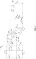
- Fig. 1 shows an example implementation of a buck converter 10 having a PSFB topology that may be controlled to operate as a boost converter.
- Converter 10 includes a low voltage side 11 and a high voltage side 12.
- the low voltage side is so named because it receives and/or outputs a low voltage and the high voltage side is so named because it receives and/or outputs a high voltage.
- "High” and “low” have no specific numerical connotations, but rather are meant only to indicate that the voltage on the high voltage side is greater than the voltage on the low voltage side.
- the high voltage side is referred to as the primary side and the low voltage side is referred to as the secondary side.
- a transformer 14 operates as the electrical interface between the low voltage side 11 and the high voltage side 12.
- transformer 14 includes a primary winding 15 and two secondary windings 16 and 17.
- Converter 10 also include transistors 19 and 21.
- the transistors are power metal oxide field-effect (MOSFET) transistors, which are controllable to operate as synchronous rectification switches to control the operation of converter 10. As shown, drain 22 of transistor 19 is connected to terminal 24 of secondary winding 17 and drain 25 of transistor 21 is connected to terminal 26 of secondary winding 16.
- MOSFET power metal oxide field-effect
- inductor 31 is connected to the center tap of transformer 14 between secondary windings 16 and 17. As also shown, inductor 31 is connected in series with capacitor bank 32 and the output terminal 40 of converter 10. A load (not shown) - for example, a device to be driven by the voltage output of the buck converter - may be connected to the output terminal. Depending on how the transistors are switched, a square wave voltage is generated and applied through inductor 31. Capacitor bank 32 is connected in parallel between the load and electrical ground 37. Inductor 31, in combination with capacitor bank 32, filters that square wave voltage to limit ripple in the voltage provided to the load. Sources 34 and 35 of respective transistors 19 and 21 are also connected to electrical ground in this example.
- an input voltage - PWM control signals are applied to the gates of transistors 19 and 21 (and also to transistors 41, 42, 43, and 44 discussed below) to charge the capacitor bank to produce a stepped-down output voltage.
- a high voltage input is provided to primary winding 15 and is stepped-down to produce a lower voltage at secondary windings 16 and 17.
- transistor 19 conducts.
- no control signal e.g., zero volts
- transistor 21 does not conduct during this time.
- a PWM signal is applied to the gate of transistor 21, thereby causing transistor 21 to conduct.
- no control signal is applied to transistor 19.
- transistor 19 does not conduct during this time.
- the current through inductor 31 discharges to maintain the voltage across the load. This cycle repeats to maintain the stepped-down voltage across the load.
- the high voltage side 12 of converter 10 includes transistors 41, 42, 43, and 44.
- Transistors 41, 42, 43, and 44 form the PSFB, which is configured and controllable to switch a DC input voltage at voltage rails 47 and 48 to produce an alternating DC voltage or square wave DC voltage at primary winding 15 of transformer 14.
- Capacitor 50 is a blocking capacitor that is used to ensure that transformer 14 does not become unbalanced. For example, when the voltages on either side of transformer 14 are reversed, excessive flux can develop in one direction that may cause the transformer to saturate and not operate normally.
- Capacitor 50 limits the passage of unbalanced DC current to the transformer and prevents or reduces saturation of the transformer.
- Resistor 51 is sized to ensure that capacitor 50 balances and discharges within an acceptable timeframe.
- the high voltage side also includes clamp diodes 52, 53. In some implementations, clamp diodes 52, 53 are not included. Clamp diodes 52 and 53 clamp the high-frequency ringing voltage at node 55 between primary winding 15 (a leakage inductance of transformer 14), the capacitance of transistors 19 and 21 on the low voltage side, and the resonant inductor 57 to the input voltage rails 47 and 48. This reduces the current through the transformer windings and resonant inductor 57, which may alleviate or prevent voltage ringing on the low voltage side of the transformer on the drains of transistors 19 and 21. Resonant inductor 57 provides energy storage for the PSFB to operate in a zero voltage switched (ZVS) mode of operation.
- ZVS zero voltage switched
- converter 10 is controllable to operate in a boost mode - for example, to discharge capacitor bank 32 through transformer 14.
- boost mode power flows in the direction of arrow 60
- boost mode power flows in the direction of arrow 61.
- the charge stored in capacitor bank 32 is used to produce a voltage output at the primary winding 15 of transformer 14.
- transistors 41, 42, 43, and 44 include MOSFETs. When zero volts is applied to their gates, the MOSFETs operate as diodes due to their internal body diodes. Accordingly, during boost mode, converter 10 may be modeled as shown in Fig. 2 . That is, transistors 41, 42, 43, and 44 are modeled as respective diodes 64, 65, 66, and 67. The remaining features of Fig. 2 are the same as those of Fig. 1 , except that an additional resistor 70 may be added to measure inductor current.
- transistors 19 and 21 are controlled by applying PWM signals to their respective gates.
- Transistors 19 and 21 are controlled to connect the capacitor bank along a current path to the transformer that runs through at least one of the transistors to enable the capacitor bank to discharge through the transformer.
- the PWM signals are generated based, at least in part, on current from the low voltage side 11 to the high voltage side 12.
- the PWM signals are generated to regulate that current so that the current does not exceed the current limit of the converter and thereby cause damage to the buck converter circuitry.
- an example of a traditional operation of synchronous rectification transistors in a voltage converter includes applying, to the gates of the synchronous rectification transistors, signals that have the same period and that are out-of-phase.
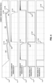
- Fig. 3 includes timing diagrams 71, 72, 73, 74, and 75 that illustrate an example operation of converter 10 in boost mode.
- the X-axis includes time and the Y-axis includes current or voltage as indicated below.
- Timing diagram 71 shows the current through inductor 31. The current is depicted as negative (less than zero amperes ("0 A" in the figure)), since the current is flowing in the direction of arrow 61 in Fig. 1 . That is, negative current is designated as current flowing away from the capacitor bank or load and towards transformer 14, whereas positive current is designated as current flowing away from transformer 14 and towards the capacitor bank or load.
- Timing diagram 72 shows the voltage on the drain 22 of transistor 19, and timing diagram 73 shows the voltage on the drain 25 of transistor 21.
- Timing diagram 74 shows the PWM control signal applied to the gate of transistor 19; and timing diagram 75 shows the PWM control signal applied to the gate of transistor 21.
- a positive peak in the negative current through inductor 31 coincides with a change in voltage at the drain of the synchronous rectification transistor that is not conducting.
- a positive peak 78 indicates a change in slope - that is, a decrease followed by an increase - in current through inductor 31.
- positive peak 78 coincides with a decrease in voltage 79 at the drain of non-conducting transistor 21.
- each positive peak represents a local minimum current through the inductor.
- the minimum is characterized as local because it may fluctuate from cycle-to-cycle.
- the current begins to circulate internally within the high voltage side of the transformer or on the primary winding of the transformer and is not transferred out to the input at nodes 47 and 48. That current, if unchecked, can cause damage to the converter. Accordingly, when a decrease in voltage 79 is detected at the drain of non-conducting transistor 21, transistor 21 is driven to conduction by applying a non-zero voltage 80 to its gate 23. This produces a controlled increase 84 in current through inductor 31.
- the drain voltages on the synchronous rectification transistors provide information about how current is transferring on the primary side of the transformer. Accordingly, use of the drain voltages on the synchronous rectification transistors enables control over the converter based on the current in the primary winding and how power flows into the input at 47 and 48 without directly measuring that current. As explained above, that control causes a synchronous rectification transistor to switch once the current stops flowing out of the converter into the input.
- transistor 19 remains conductive temporarily 85 while transistor 21 is driven to conduction.
- use of a center-tapped secondary winding may require that transistors 19 and 21 always have some temporary conduction overlap in order to keep secondary voltage spikes down.
- overlap 85 in operation between transistors 19 and 21.
- both of transistors 19 and 21 are non-conductive at the same time, all of the energy from the transformer may instantly transfer to those transistors as a high voltage spike. This could damage the transistors.
- the temporary overlap in conduction between transistors 19 and 21 may reduce the chances that this type of damage will occur.
- a maximum negative current through the transformer is detected.
- This maximum negative current is represented by negative peak 88 in timing diagram 71.
- the maximum negative current may have a predefined magnitude that is based on operational characteristics of the transformer and other circuitry used to implement the buck converter. Exceeding the maximum negative current could result in damage to the circuitry. Accordingly, at that time, transistor 19, which is already conducting as shown in timing diagram 74, is made non-conductive by applying a zero voltage 90 to its gate 33. This produces a controlled decrease 92 in current through the inductor, as shown in timing diagram 71.
- the system may be able automatically to adjust for variations in input and output voltage, temperature, and component value variations.
- the controlled decrease 92 in current continues until another positive peak 95 occurs.
- the voltage 97 on the drain 22 of transistor 19 decreases, as shown in timing diagram 72.
- transistor 19 - the previously non-conductive transistor - is driven to conduction by applying a non-zero voltage 99 to its gate 33.
- transistor 21 remains temporarily conductive 101 while transistor 19 is driven to conduction.
- a maximum negative current through the inductor is detected.
- This maximum negative current is represented by negative peak 103 in timing diagram 71.
- transistor 21, which is already conducting as shown in timing diagram 75 is made non-conductive by applying a zero voltage 104 to its gate 23. This produces a controlled decrease 106 in current through the inductor, as shown in timing diagram 71.
- the foregoing process repeats to provide controlled current flow from the low voltage side of the buck converter to the high voltage side of the buck converter. In the examples described herein, the foregoing process repeats until the capacitor bank is discharged to zero volts or substantially zero volts.
- the example circuitry of Figs. 1 and 2 also includes components (not shown) to detect voltages on the drains of transistors 19 and 21 and negative peaks of the inductor current.
- the circuitry may include multiple analog comparators.
- One or more comparators may be used to detect voltages on the drains of transistors 19 and 21.
- a first comparator may be used to detect the voltage on the drain 22 of transistor 19 and a second, different comparator may be used to detect the voltage on the drain 25 of transistor 21.
- a single comparator may be used to detect the voltage on the drain 22 of transistor 19 and to detect the voltage on the drain 25 of transistor 21. In this example, detection of drain voltage on a single transistor, such as transistor 19, is performed every other clock cycle.
- components to detect the negative peak of the inductor current include one or more of the analog comparators.
- an analog comparator compares the inductor current to a predefined threshold. When that threshold is reached, the maximum negative current is detected.
- Resistor 70 may also be included to detect the current through inductor 31.
- the detected drain voltages and the time at which the maximum negative current (the negative peak) is detected may be digitized and transmitted to the control system.
- the control system uses the resulting data to control the gates of transistors 19 and 21 in the manner described with respect to timing diagrams 74 and 75.
- Fig. 4 includes timing diagrams 110, 111, 112, 113, and 114 that illustrate another example operation of converter 10 in boost mode. Comparing Fig. 4 to Fig. 3 , it is evident that the decreasing inductor current - for example, decreases 92 and 116 - occurs at a lower rate in Fig. 4 than in Fig. 3 . This is due to characteristics of the transformer and converter operating point such as input and output voltage at an instant in time. In the example of Fig. 3 , the turns ratio of the transformer can support an input voltage that is greater than the voltage that can be generated by the low voltage side of the converter. In the example of Fig.
- the turns ratio of the transformer can support an input voltage that is greater than the voltage that can be generated by the low voltage side of the converter, but not as great as the voltage that can be supported by the transformer turns ratio in the example of Fig. 3 .
- the transformer turns ratio is configured to support a higher voltage than a combined voltage of the first secondary winding and the second secondary winding taking into account a turns ratio of the transformer.
- a transformer having appropriate numbers of windings and ratios may be selected.
- the primary winding may be configured to support a higher voltage than a combined voltage of the first secondary winding and the second secondary winding multiplied by a turns ratio of the transformer.
- timing diagram 110 shows the current through inductor 31 of Figs. 1 and 2 .
- the current is depicted as negative, since it is flowing in the direction of arrow 61 in Fig. 1 .
- Timing diagram 111 shows the voltage on the drain 22 of transistor 19, and timing diagram 112 shows the voltage on the drain 25 of transistor 21.
- Timing diagram 113 shows the PWM control signal applied to the gate of transistor 19; and timing diagram 14 shows the PWM control signal applied to the gate of transistor 21.
- a positive peak in the negative current through inductor 31 coincides with a change in voltage at the drain of the synchronous rectification transistor that is not conducting.
- positive peak 118 coincides with a decrease in voltage 119 at drain 25 of transistor 21, as shown in timing diagram 112.
- transistor 21 is driven to conduction by applying a non-zero voltage 121 to its gate 23. This produces a controlled increase 122 in current through inductor 31. As shown in timing diagram 113, transistor 19 remains conductive for a time 124 while transistor 21 is driven to conduction.
- transistor 19 which is already conducting as shown in timing diagram 113, is made non-conductive by applying a zero voltage 127 to its gate 33. This produces a controlled decrease 128 in current through the inductor, as shown in timing diagram 110.
- the controlled decrease 128 continues until positive peak 130 is detected.
- the voltage 131 on the drain 22 of transformer 19 decreases, as shown in timing diagram 111.
- transistor 19 - the previously non-conductive transistor - is driven to conduction by applying a non-zero voltage 133 to its gate 33.
- transistor 21 remains conductive while transistor 19 is driven to conduction.
- a maximum negative current through the transformer is detected.
- This maximum negative current is represented by negative peak 135 in timing diagram 110.
- transistor 21, which is already conducting as shown in timing diagram 113 is made non-conductive by applying a zero voltage 137 to its gate 23. This produces a controlled decrease in current through the inductor, as shown in timing diagram 110.
- the foregoing process repeats to provide controlled current from the low voltage side of the converter to the high voltage side of the converter. In the examples described herein, the foregoing process repeats until the capacitor bank is discharged to zero volts or substantially zero volts.
- the example systems and processes described herein may be used in any appropriate electronic system.
- the systems and processes may be used in DC/DC converters within radar systems, antenna systems, or radar and antenna systems.
- the systems and processes may be used in power supply systems in any appropriate technological context.
- All or part of the systems and processes described in this specification and their various modifications may be configured or controlled at least in part by a control system that includes one or more computers executing one or more computer programs tangibly embodied in one or more information carriers, such as in one or more non-transitory machine-readable storage media.
- the PWM signals may be generated by one or more computers using one or more computer programs based on voltages detected on the synchronous rectification transistors' drains and the maximum negative current detected in the inductor.
- a computer program can be written in any form of programming language, including compiled or interpreted languages, and it can be deployed in any form, including as a stand-alone program or as a module, part, subroutine, or other unit suitable for use in a computing environment.
- a computer program can be deployed to be executed on one computer or on multiple computers at one site or distributed across multiple sites and interconnected by a network.
- Actions associated with configuring or controlling the systems and processes can be performed by one or more programmable processors executing one or more computer programs to control all or some of the well formation operations described previously. All or part of the systems and processes can be configured or controlled by special purpose logic circuitry, such as, an FPGA (field programmable gate array) and/or an ASIC (application-specific integrated circuit).
- special purpose logic circuitry such as, an FPGA (field programmable gate array) and/or an ASIC (application-specific integrated circuit).
- processors suitable for the execution of a computer program include, by way of example, both general and special purpose microprocessors, and any one or more processors of any kind of digital computer.
- a processor will receive instructions and data from a read-only storage area or a random access storage area or both.
- Elements of a computer include one or more processors for executing instructions and one or more storage area devices for storing instructions and data.
- a computer will also include, or be operatively coupled to receive data from, or transfer data to, or both, one or more machine-readable storage media, such as mass storage devices for storing data, such as magnetic, magneto-optical disks, or optical disks.
- Non-transitory machine-readable storage media suitable for embodying computer program instructions and data include all forms of non-volatile storage area, including by way of example, semiconductor storage area devices, such as EPROM (erasable programmable read-only memory), EEPROM (electrically erasable programmable read-only memory), and flash storage area devices; magnetic disks, such as internal hard disks or removable disks; magneto-optical disks; and CD-ROM (compact disc read-only memory) and DVD-ROM (digital versatile disc read-only memory).
- semiconductor storage area devices such as EPROM (erasable programmable read-only memory), EEPROM (electrically erasable programmable read-only memory), and flash storage area devices
- magnetic disks such as internal hard disks or removable disks
- magneto-optical disks magneto-optical disks
- CD-ROM compact disc read-only memory
- DVD-ROM digital versatile disc read-only memory
Landscapes
- Engineering & Computer Science (AREA)
- Power Engineering (AREA)
- Physics & Mathematics (AREA)
- Electromagnetism (AREA)
- General Physics & Mathematics (AREA)
- Radar, Positioning & Navigation (AREA)
- Automation & Control Theory (AREA)
- Dc-Dc Converters (AREA)
Claims (15)
- Convertisseur de tension (10) comprenant :un transformateur (14) comprenant un enroulement primaire (15), un premier enroulement secondaire (16) et un second enroulement secondaire (17) ;un premier transistor (21) connecté entre une première borne du premier enroulement secondaire (16) et la masse électrique, le premier transistor comprenant un premier drain (25) ;un second transistor (19) connecté entre une seconde borne du second enroulement secondaire (17) et la masse électrique, le second transistor comprenant un second drain (22) ;un condensateur (32) qui peut être connecté le long d'un trajet de courant au transformateur (14) via au moins l'un du premier transistor (21) ou du second transistor (19) ;un système de contrôle configuré pour détecter une première tension au niveau du premier drain (25) et une seconde tension au niveau du second drain (22), et pour générer des signaux de contrôle modulés en largeur d'impulsion sur la base au moins de la première tension et de la seconde tension, les signaux de contrôle modulés en largeur d'impulsion étant configurés pour contrôler le fonctionnement du premier transistor (21) et du second transistor (19) afin de produire une tension au niveau de l'enroulement primaire (15) sur la base d'une tension aux bornes du condensateur (32) ; etune borne de sortie (40) configurée pour être connectée à une charge ;le convertisseur de tension étant caractérisé par :un inducteur (31) connecté en série avec le condensateur (32) et la borne de sortie (41) et connecté au niveau d'une prise centrale du transformateur (14) entre le premier enroulement secondaire (16) et le second enroulement secondaire (17) ;dans lequel les signaux de contrôle modulés en largeur d'impulsion sont également basés sur le courant traversant l'inducteur (31) jusqu'au transformateur (14).
- Convertisseur de tension selon la revendication 1, dans lequel les signaux de contrôle modulés en largeur d'impulsion sont configurés pour contrôler le fonctionnement du premier transistor (21) et du second transistor (19) pour permettre la décharge du condensateur (32) via l'inducteur (31).
- Convertisseur de tension selon la revendication 1, dans lequel le premier transistor (21) comprend une première grille et le second transistor (19) comprend une seconde grille ; et dans lequel le système de contrôle est configuré pour appliquer les signaux de contrôle modulés en largeur d'impulsion à la première grille et à la seconde grille.
- Convertisseur de tension selon la revendication 3, dans lequel le système de contrôle est configuré pour détecter le moment où la première tension diminue ; et
dans lequel le système de contrôle est configuré pour générer un premier signal de contrôle modulé en largeur d'impulsion à appliquer à la première grille en réponse à la première diminution de tension, le premier signal de contrôle modulé en largeur d'impulsion ayant une largeur d'impulsion qui est également basée sur le courant traversant l'inducteur (31). - Convertisseur de tension selon la revendication 4, dans lequel le système de contrôle est configuré pour identifier le moment où la seconde tension diminue ; et
dans lequel le système de contrôle est configuré pour générer un second signal de contrôle modulé en largeur d'impulsion à appliquer à la seconde grille en réponse à la seconde diminution de tension, le second signal de contrôle modulé en largeur d'impulsion ayant une largeur d'impulsion qui est également basée sur le courant traversant l'inducteur (31). - Convertisseur de tension selon la revendication 4, dans lequel un instant où la première tension diminue correspond à un courant minimal traversant le transformateur (14).
- Convertisseur de tension selon la revendication 6, dans lequel le courant minimal traversant le transformateur (14) correspond à la circulation de courant sur un côté tension primaire ou l'enroulement primaire du transformateur (14).
- Convertisseur de tension selon la revendication 1, comprenant en outre :des transistors d'entrée connectés électriquement à l'enroulement primaire (15) ;dans lequel le système de contrôle est configuré pour appliquer des signaux de contrôle aux grilles des transistors d'entrée afin de faire fonctionner les transistors d'entrée comme des diodes.
- Convertisseur de tension selon la revendication 1, comprenant en outre :
des diodes de serrage connectées entre des rails de tension sur un côté enroulement primaire (15) du transformateur (14), les diodes de serrage étant configurées pour réduire une oscillation de tension sur un côté tension secondaire du transformateur (14) . - Convertisseur de tension selon la revendication 1, dans lequel le système de contrôle comprend des comparateurs configurés pour comparer la première tension et la seconde tension à des tensions de référence.
- Convertisseur de tension selon la revendication 1, comprenant en outre :
un second inducteur (57) connecté en série avec l'enroulement primaire (15), le second inducteur (57) étant configuré pour fournir un stockage pour un pont complet déphasé afin de fonctionner dans un mode de fonctionnement à commutation de tension nulle (ZVS). - Convertisseur de tension selon la revendication 1, dans lequel le convertisseur de tension comprend un convertisseur abaisseur ; et
dans lequel, pour contrôler le fonctionnement du premier transistor (21) et du second transistor (19) pour produire la tension au niveau de l'enroulement primaire (15) sur la base de la tension aux bornes du condensateur (32), le système de contrôle est configuré pour contrôler le convertisseur abaisseur pour fonctionner comme un convertisseur élévateur. - Convertisseur de tension selon la revendication 1, dans lequel l'enroulement primaire (15) est configuré pour supporter une tension supérieure à une tension combinée du premier enroulement secondaire (16) et du second enroulement secondaire (17) multipliée par un rapport de rotation du transformateur (14) .
- Convertisseur de tension selon la revendication 1, comprenant en outre :un circuit configuré pour détecter le courant traversant l'inducteur (31) jusqu'au transformateur (14) ;dans lequel chaque signal de contrôle modulé en largeur d'impulsion a un front montant qui correspond à une diminution de la première tension ou de la seconde tension et a un front descendant qui correspond à un courant prédéfini traversant l'inducteur (31).
- Procédé de contrôle d'un convertisseur de tension (10) comprenant :la fourniture d'un transformateur (14) comprenant un enroulement primaire (15), un premier enroulement secondaire (16) et un second enroulement secondaire (17) ;la fourniture d'un premier transistor (21) connecté entre une première borne du premier enroulement secondaire (16) et la masse électrique, le premier transistor comprenant un premier drain (25) ;la fourniture d'un second transistor (19) connecté entre une seconde borne du second enroulement secondaire (17) et la masse électrique, le second transistor comprenant un second drain (22) ;la connexion d'un condensateur (32) le long d'un trajet de courant au transformateur (14) via au moins l'un du premier transistor (21) ou du second transistor (19) ;la fourniture d'un système de contrôle configuré pour détecter une première tension au niveau du premier drain (25) et une seconde tension au niveau du second drain (22) ;la génération de signaux de contrôle modulés en largeur d'impulsion sur la base au moins de la première tension et de la seconde tension, les signaux de contrôle modulés en largeur d'impulsion étant configurés pour contrôler le fonctionnement du premier transistor (21) et du second transistor (19) pour produire une tension au niveau de l'enroulement primaire (15) sur la base d'une tension aux bornes du condensateur (32) ;la connexion d'une borne de sortie (41) à une charge ;la connexion d'un inducteur (31) en série avec le condensateur (32) et la borne de sortie (41) ; etla connexion de l'inducteur (31) à une prise centrale du transformateur (14) entre le premier enroulement secondaire (16) et le second enroulement secondaire (17) ;dans lequel les signaux de contrôle modulés en largeur d'impulsion sont également basés sur le courant traversant l'inducteur (31) jusqu'au transformateur (14).
Applications Claiming Priority (2)
| Application Number | Priority Date | Filing Date | Title |
|---|---|---|---|
| US16/657,353 US10985664B1 (en) | 2019-10-18 | 2019-10-18 | Controlling operation of a voltage converter based on transistor drain voltages |
| PCT/US2020/031578 WO2021076189A1 (fr) | 2019-10-18 | 2020-05-06 | Commande de fonctionnement d'un convertisseur de tension sur la base de tensions de drain de transistor |
Publications (2)
| Publication Number | Publication Date |
|---|---|
| EP3977609A1 EP3977609A1 (fr) | 2022-04-06 |
| EP3977609B1 true EP3977609B1 (fr) | 2024-08-07 |
Family
ID=70847552
Family Applications (1)
| Application Number | Title | Priority Date | Filing Date |
|---|---|---|---|
| EP20728323.5A Active EP3977609B1 (fr) | 2019-10-18 | 2020-05-06 | Contrôle du fonctionnement d'un convertisseur de tension basé sur les tensions de drain des transistors. |
Country Status (5)
| Country | Link |
|---|---|
| US (1) | US10985664B1 (fr) |
| EP (1) | EP3977609B1 (fr) |
| AU (1) | AU2020366256B2 (fr) |
| FI (1) | FI3977609T3 (fr) |
| WO (1) | WO2021076189A1 (fr) |
Families Citing this family (1)
| Publication number | Priority date | Publication date | Assignee | Title |
|---|---|---|---|---|
| US11804782B2 (en) * | 2022-01-28 | 2023-10-31 | Analog Devices, Inc. | Active-clamp current-fed push-pull converter for bidirectional power transfer |
Family Cites Families (29)
| Publication number | Priority date | Publication date | Assignee | Title |
|---|---|---|---|---|
| US6111769A (en) | 1999-09-24 | 2000-08-29 | Ericsson, Inc. | External driving circuit for bridge type synchronous rectification |
| US6426884B1 (en) | 2000-11-06 | 2002-07-30 | Ericsson, Inc. | Reducing reverse currents in a synchronous rectifier circuit |
| US6618274B2 (en) | 2001-10-09 | 2003-09-09 | Innoveta Technologies | Synchronous rectifier controller to eliminate reverse current flow in a DC/DC converter output |
| US7548435B2 (en) * | 2006-03-31 | 2009-06-16 | Astec International Limited | Zero-voltage-switching DC-DC converters with synchronous rectifiers |
| US8373403B1 (en) | 2008-08-08 | 2013-02-12 | Power-One, Inc. | Circuit for controlling synchronous rectifiers during start-up into pre-biased output voltage |
| US8929106B2 (en) | 2011-05-20 | 2015-01-06 | General Electric Company | Monotonic pre-bias start-up of a DC-DC converter |
| US20120320633A1 (en) | 2011-06-16 | 2012-12-20 | Chang-Hsing Chen | Variable frequency pwm synchronous rectifier power supply |
| US8749217B2 (en) | 2011-06-29 | 2014-06-10 | Texas Instruments Incorporated | Primary voltage sensing and control for converter |
| US20140009970A1 (en) | 2012-07-06 | 2014-01-09 | Power Systems Technologies, Ltd. | Controller for a Power Converter and Method of Operating the Same |
| US9190898B2 (en) | 2012-07-06 | 2015-11-17 | Power Systems Technologies, Ltd | Controller for a power converter and method of operating the same |
| US9083255B2 (en) | 2012-11-19 | 2015-07-14 | Analog Devices, Inc. | Adaptive dead time control scheme for switch mode power converter with synchronous rectifiers topology |
| US9099932B2 (en) | 2013-01-07 | 2015-08-04 | Analog Devices Global | Duty cycle balance module for switch mode power converter |
| US9438127B2 (en) | 2013-03-11 | 2016-09-06 | Analog Devices Global | Reverse current control for an isolated power supply having synchronous rectifiers |
| US9859803B2 (en) | 2013-04-23 | 2018-01-02 | Analog Devices Global | Transformer-based isolated bi-directional DC-DC power converter, and method and controller for using same |
| US9350259B2 (en) | 2013-07-31 | 2016-05-24 | Analog Devices Global | Synchronous rectifier control for a double-ended isolated power converter |
| US9252672B2 (en) | 2013-10-04 | 2016-02-02 | Chicony Power Technology Co., Ltd. | Method of controlling phase-shift full-bridge converter in light load operation |
| US20150098254A1 (en) | 2013-10-09 | 2015-04-09 | Power Systems Technologies Ltd. | Controller for use with a power converter and method of operating the same |
| US20150194900A1 (en) | 2014-01-06 | 2015-07-09 | Bel Fuse (Macao Commercial Offshore) Limited | Power converter with modulated secondary-side synchronous rectification |
| US9337741B2 (en) | 2014-02-17 | 2016-05-10 | Huawei Technologies Co., Ltd. | DC-DC conversion circuit and method |
| US9831790B2 (en) | 2014-09-17 | 2017-11-28 | Alps Electric Co., Ltd. | DC-to-DC converter |
| US9379621B1 (en) | 2015-01-28 | 2016-06-28 | Microchip Technology Incorporated | Digital slope compensation for peak current controlled converters |
| US10277130B2 (en) | 2015-06-01 | 2019-04-30 | Microchip Technolgoy Incorporated | Primary-side start-up method and circuit arrangement for a series-parallel resonant power converter |
| KR102485478B1 (ko) | 2015-12-14 | 2023-01-06 | 현대모비스 주식회사 | 차량의 dc-dc 컨버터의 역전류 방지 장치 및 그 동작 방법 |
| US9825546B2 (en) | 2016-03-30 | 2017-11-21 | Infineon Technologies Austria Ag | Circuits and methods for auxiliary secondary supply generation with self-starting primary side driver in isolated power converters |
| US10284099B2 (en) | 2016-06-07 | 2019-05-07 | Linear Technology Corporation | Hybrid power converters combining switched-capacitor and transformer-based stages |
| US9812971B1 (en) | 2016-08-12 | 2017-11-07 | Infineon Technologies Austria Ag | Transformer flux estimation and limiting in isolated DC-DC voltage converters |
| JP6932633B2 (ja) | 2017-12-25 | 2021-09-08 | Fdk株式会社 | スイッチング電源装置 |
| JP7048326B2 (ja) * | 2018-01-17 | 2022-04-05 | ローム株式会社 | 絶縁同期整流型dc/dcコンバータ |
| US10601333B2 (en) | 2018-08-22 | 2020-03-24 | Infineon Technologies Austria Ag | Feedforward enhanced feedback control in isolated switched-mode power converters with secondary-side rectified voltage sensing |
-
2019
- 2019-10-18 US US16/657,353 patent/US10985664B1/en active Active
-
2020
- 2020-05-06 AU AU2020366256A patent/AU2020366256B2/en active Active
- 2020-05-06 WO PCT/US2020/031578 patent/WO2021076189A1/fr not_active Ceased
- 2020-05-06 EP EP20728323.5A patent/EP3977609B1/fr active Active
- 2020-05-06 FI FIEP20728323.5T patent/FI3977609T3/fi active
Also Published As
| Publication number | Publication date |
|---|---|
| WO2021076189A1 (fr) | 2021-04-22 |
| US20210119545A1 (en) | 2021-04-22 |
| US10985664B1 (en) | 2021-04-20 |
| FI3977609T3 (fi) | 2024-08-22 |
| AU2020366256B2 (en) | 2024-11-28 |
| EP3977609A1 (fr) | 2022-04-06 |
| AU2020366256A1 (en) | 2021-12-23 |
Similar Documents
| Publication | Publication Date | Title |
|---|---|---|
| US11824453B2 (en) | Secondary controller for use in synchronous flyback converter | |
| EP3977610B1 (fr) | Contrôle du fonctionnement d'un convertisseur de tension basé sur le courant inducteur | |
| EP3664295B1 (fr) | Commande de commutateur à deux niveaux pour empêcher un effet d'avalanche pour un commutateur de redressement synchrone dans un convertisseur de puissance fonctionnant en mode rafale à faible puissance | |
| US6396250B1 (en) | Control method to reduce body diode conduction and reverse recovery losses | |
| US10211719B2 (en) | Power converter | |
| US9407156B2 (en) | Managing leakage inductance in a power supply | |
| US9531250B2 (en) | Power conversion device and refrigeration/air-conditioning system | |
| US9825521B2 (en) | Method and apparatus for inductive-kick protection clamp during discontinuous conduction mode operation | |
| EP3731393A1 (fr) | Convertisseur cc-cc à amortissement lc à commutation séquentielle et circuit régénératif | |
| CN114793068A (zh) | 电源转换器以及用于操作电源转换器的方法和控制器 | |
| US8503195B1 (en) | System and method for zero volt switching of half bridge converters during startup and short circuit conditions | |
| US11843320B2 (en) | Method of operating isolated resonant converter with synchronous rectifier | |
| EP3977609B1 (fr) | Contrôle du fonctionnement d'un convertisseur de tension basé sur les tensions de drain des transistors. | |
| US20060187692A1 (en) | Output voltage control of a synchronous rectifier | |
| EP4005079B1 (fr) | Circuit de commande de prédémarrage d'un convertisseur de puissance de commutation comprenant un commutateur redresseur synchrone sur le côté secondaire d'une section de stockage d'énergie | |
| JP4383946B2 (ja) | 電源装置 | |
| JP2005304165A (ja) | 電源装置 | |
| JP2016134951A (ja) | 逆電流保護付きスイッチング電源装置 |
Legal Events
| Date | Code | Title | Description |
|---|---|---|---|
| STAA | Information on the status of an ep patent application or granted ep patent |
Free format text: STATUS: UNKNOWN |
|
| STAA | Information on the status of an ep patent application or granted ep patent |
Free format text: STATUS: THE INTERNATIONAL PUBLICATION HAS BEEN MADE |
|
| PUAI | Public reference made under article 153(3) epc to a published international application that has entered the european phase |
Free format text: ORIGINAL CODE: 0009012 |
|
| STAA | Information on the status of an ep patent application or granted ep patent |
Free format text: STATUS: REQUEST FOR EXAMINATION WAS MADE |
|
| 17P | Request for examination filed |
Effective date: 20211228 |
|
| AK | Designated contracting states |
Kind code of ref document: A1 Designated state(s): AL AT BE BG CH CY CZ DE DK EE ES FI FR GB GR HR HU IE IS IT LI LT LU LV MC MK MT NL NO PL PT RO RS SE SI SK SM TR |
|
| DAV | Request for validation of the european patent (deleted) | ||
| DAX | Request for extension of the european patent (deleted) | ||
| REG | Reference to a national code |
Ref legal event code: R079 Free format text: PREVIOUS MAIN CLASS: H02M0003335000 Ipc: H02M0003156000 Ref country code: DE Ref legal event code: R079 Ref document number: 602020035298 Country of ref document: DE Free format text: PREVIOUS MAIN CLASS: H02M0003335000 Ipc: H02M0003156000 |
|
| GRAP | Despatch of communication of intention to grant a patent |
Free format text: ORIGINAL CODE: EPIDOSNIGR1 |
|
| RIC1 | Information provided on ipc code assigned before grant |
Ipc: H02M 3/335 20060101ALI20230929BHEP Ipc: H02M 3/156 20060101AFI20230929BHEP |
|
| STAA | Information on the status of an ep patent application or granted ep patent |
Free format text: STATUS: GRANT OF PATENT IS INTENDED |
|
| INTG | Intention to grant announced |
Effective date: 20231109 |
|
| GRAJ | Information related to disapproval of communication of intention to grant by the applicant or resumption of examination proceedings by the epo deleted |
Free format text: ORIGINAL CODE: EPIDOSDIGR1 |
|
| STAA | Information on the status of an ep patent application or granted ep patent |
Free format text: STATUS: REQUEST FOR EXAMINATION WAS MADE |
|
| GRAP | Despatch of communication of intention to grant a patent |
Free format text: ORIGINAL CODE: EPIDOSNIGR1 |
|
| STAA | Information on the status of an ep patent application or granted ep patent |
Free format text: STATUS: GRANT OF PATENT IS INTENDED |
|
| INTC | Intention to grant announced (deleted) | ||
| INTG | Intention to grant announced |
Effective date: 20240318 |
|
| GRAS | Grant fee paid |
Free format text: ORIGINAL CODE: EPIDOSNIGR3 |
|
| GRAA | (expected) grant |
Free format text: ORIGINAL CODE: 0009210 |
|
| STAA | Information on the status of an ep patent application or granted ep patent |
Free format text: STATUS: THE PATENT HAS BEEN GRANTED |
|
| AK | Designated contracting states |
Kind code of ref document: B1 Designated state(s): AL AT BE BG CH CY CZ DE DK EE ES FI FR GB GR HR HU IE IS IT LI LT LU LV MC MK MT NL NO PL PT RO RS SE SI SK SM TR |
|
| REG | Reference to a national code |
Ref country code: GB Ref legal event code: FG4D |
|
| REG | Reference to a national code |
Ref country code: CH Ref legal event code: EP |
|
| REG | Reference to a national code |
Ref country code: FI Ref legal event code: FGE |
|
| REG | Reference to a national code |
Ref country code: IE Ref legal event code: FG4D |
|
| REG | Reference to a national code |
Ref country code: DE Ref legal event code: R096 Ref document number: 602020035298 Country of ref document: DE |
|
| REG | Reference to a national code |
Ref country code: LT Ref legal event code: MG9D |
|
| REG | Reference to a national code |
Ref country code: NL Ref legal event code: MP Effective date: 20240807 |
|
| PG25 | Lapsed in a contracting state [announced via postgrant information from national office to epo] |
Ref country code: NO Free format text: LAPSE BECAUSE OF FAILURE TO SUBMIT A TRANSLATION OF THE DESCRIPTION OR TO PAY THE FEE WITHIN THE PRESCRIBED TIME-LIMIT Effective date: 20241107 |
|
| REG | Reference to a national code |
Ref country code: AT Ref legal event code: MK05 Ref document number: 1712029 Country of ref document: AT Kind code of ref document: T Effective date: 20240807 |
|
| PG25 | Lapsed in a contracting state [announced via postgrant information from national office to epo] |
Ref country code: NL Free format text: LAPSE BECAUSE OF FAILURE TO SUBMIT A TRANSLATION OF THE DESCRIPTION OR TO PAY THE FEE WITHIN THE PRESCRIBED TIME-LIMIT Effective date: 20240807 Ref country code: PL Free format text: LAPSE BECAUSE OF FAILURE TO SUBMIT A TRANSLATION OF THE DESCRIPTION OR TO PAY THE FEE WITHIN THE PRESCRIBED TIME-LIMIT Effective date: 20240807 Ref country code: PT Free format text: LAPSE BECAUSE OF FAILURE TO SUBMIT A TRANSLATION OF THE DESCRIPTION OR TO PAY THE FEE WITHIN THE PRESCRIBED TIME-LIMIT Effective date: 20241209 Ref country code: GR Free format text: LAPSE BECAUSE OF FAILURE TO SUBMIT A TRANSLATION OF THE DESCRIPTION OR TO PAY THE FEE WITHIN THE PRESCRIBED TIME-LIMIT Effective date: 20241108 |
|
| PG25 | Lapsed in a contracting state [announced via postgrant information from national office to epo] |
Ref country code: BG Free format text: LAPSE BECAUSE OF FAILURE TO SUBMIT A TRANSLATION OF THE DESCRIPTION OR TO PAY THE FEE WITHIN THE PRESCRIBED TIME-LIMIT Effective date: 20240807 |
|
| PG25 | Lapsed in a contracting state [announced via postgrant information from national office to epo] |
Ref country code: LV Free format text: LAPSE BECAUSE OF FAILURE TO SUBMIT A TRANSLATION OF THE DESCRIPTION OR TO PAY THE FEE WITHIN THE PRESCRIBED TIME-LIMIT Effective date: 20240807 |
|
| PG25 | Lapsed in a contracting state [announced via postgrant information from national office to epo] |
Ref country code: IS Free format text: LAPSE BECAUSE OF FAILURE TO SUBMIT A TRANSLATION OF THE DESCRIPTION OR TO PAY THE FEE WITHIN THE PRESCRIBED TIME-LIMIT Effective date: 20241207 Ref country code: AT Free format text: LAPSE BECAUSE OF FAILURE TO SUBMIT A TRANSLATION OF THE DESCRIPTION OR TO PAY THE FEE WITHIN THE PRESCRIBED TIME-LIMIT Effective date: 20240807 |
|
| PG25 | Lapsed in a contracting state [announced via postgrant information from national office to epo] |
Ref country code: HR Free format text: LAPSE BECAUSE OF FAILURE TO SUBMIT A TRANSLATION OF THE DESCRIPTION OR TO PAY THE FEE WITHIN THE PRESCRIBED TIME-LIMIT Effective date: 20240807 |
|
| PG25 | Lapsed in a contracting state [announced via postgrant information from national office to epo] |
Ref country code: ES Free format text: LAPSE BECAUSE OF FAILURE TO SUBMIT A TRANSLATION OF THE DESCRIPTION OR TO PAY THE FEE WITHIN THE PRESCRIBED TIME-LIMIT Effective date: 20240807 Ref country code: RS Free format text: LAPSE BECAUSE OF FAILURE TO SUBMIT A TRANSLATION OF THE DESCRIPTION OR TO PAY THE FEE WITHIN THE PRESCRIBED TIME-LIMIT Effective date: 20241107 |
|
| PG25 | Lapsed in a contracting state [announced via postgrant information from national office to epo] |
Ref country code: RS Free format text: LAPSE BECAUSE OF FAILURE TO SUBMIT A TRANSLATION OF THE DESCRIPTION OR TO PAY THE FEE WITHIN THE PRESCRIBED TIME-LIMIT Effective date: 20241107 Ref country code: PT Free format text: LAPSE BECAUSE OF FAILURE TO SUBMIT A TRANSLATION OF THE DESCRIPTION OR TO PAY THE FEE WITHIN THE PRESCRIBED TIME-LIMIT Effective date: 20241209 Ref country code: PL Free format text: LAPSE BECAUSE OF FAILURE TO SUBMIT A TRANSLATION OF THE DESCRIPTION OR TO PAY THE FEE WITHIN THE PRESCRIBED TIME-LIMIT Effective date: 20240807 Ref country code: NO Free format text: LAPSE BECAUSE OF FAILURE TO SUBMIT A TRANSLATION OF THE DESCRIPTION OR TO PAY THE FEE WITHIN THE PRESCRIBED TIME-LIMIT Effective date: 20241107 Ref country code: NL Free format text: LAPSE BECAUSE OF FAILURE TO SUBMIT A TRANSLATION OF THE DESCRIPTION OR TO PAY THE FEE WITHIN THE PRESCRIBED TIME-LIMIT Effective date: 20240807 Ref country code: LV Free format text: LAPSE BECAUSE OF FAILURE TO SUBMIT A TRANSLATION OF THE DESCRIPTION OR TO PAY THE FEE WITHIN THE PRESCRIBED TIME-LIMIT Effective date: 20240807 Ref country code: IS Free format text: LAPSE BECAUSE OF FAILURE TO SUBMIT A TRANSLATION OF THE DESCRIPTION OR TO PAY THE FEE WITHIN THE PRESCRIBED TIME-LIMIT Effective date: 20241207 Ref country code: HR Free format text: LAPSE BECAUSE OF FAILURE TO SUBMIT A TRANSLATION OF THE DESCRIPTION OR TO PAY THE FEE WITHIN THE PRESCRIBED TIME-LIMIT Effective date: 20240807 Ref country code: GR Free format text: LAPSE BECAUSE OF FAILURE TO SUBMIT A TRANSLATION OF THE DESCRIPTION OR TO PAY THE FEE WITHIN THE PRESCRIBED TIME-LIMIT Effective date: 20241108 Ref country code: ES Free format text: LAPSE BECAUSE OF FAILURE TO SUBMIT A TRANSLATION OF THE DESCRIPTION OR TO PAY THE FEE WITHIN THE PRESCRIBED TIME-LIMIT Effective date: 20240807 Ref country code: BG Free format text: LAPSE BECAUSE OF FAILURE TO SUBMIT A TRANSLATION OF THE DESCRIPTION OR TO PAY THE FEE WITHIN THE PRESCRIBED TIME-LIMIT Effective date: 20240807 Ref country code: AT Free format text: LAPSE BECAUSE OF FAILURE TO SUBMIT A TRANSLATION OF THE DESCRIPTION OR TO PAY THE FEE WITHIN THE PRESCRIBED TIME-LIMIT Effective date: 20240807 |
|
| PG25 | Lapsed in a contracting state [announced via postgrant information from national office to epo] |
Ref country code: SM Free format text: LAPSE BECAUSE OF FAILURE TO SUBMIT A TRANSLATION OF THE DESCRIPTION OR TO PAY THE FEE WITHIN THE PRESCRIBED TIME-LIMIT Effective date: 20240807 Ref country code: DK Free format text: LAPSE BECAUSE OF FAILURE TO SUBMIT A TRANSLATION OF THE DESCRIPTION OR TO PAY THE FEE WITHIN THE PRESCRIBED TIME-LIMIT Effective date: 20240807 |
|
| PG25 | Lapsed in a contracting state [announced via postgrant information from national office to epo] |
Ref country code: EE Free format text: LAPSE BECAUSE OF FAILURE TO SUBMIT A TRANSLATION OF THE DESCRIPTION OR TO PAY THE FEE WITHIN THE PRESCRIBED TIME-LIMIT Effective date: 20240807 |
|
| PG25 | Lapsed in a contracting state [announced via postgrant information from national office to epo] |
Ref country code: CZ Free format text: LAPSE BECAUSE OF FAILURE TO SUBMIT A TRANSLATION OF THE DESCRIPTION OR TO PAY THE FEE WITHIN THE PRESCRIBED TIME-LIMIT Effective date: 20240807 |
|
| PG25 | Lapsed in a contracting state [announced via postgrant information from national office to epo] |
Ref country code: SK Free format text: LAPSE BECAUSE OF FAILURE TO SUBMIT A TRANSLATION OF THE DESCRIPTION OR TO PAY THE FEE WITHIN THE PRESCRIBED TIME-LIMIT Effective date: 20240807 |
|
| REG | Reference to a national code |
Ref country code: DE Ref legal event code: R097 Ref document number: 602020035298 Country of ref document: DE |
|
| PLBE | No opposition filed within time limit |
Free format text: ORIGINAL CODE: 0009261 |
|
| STAA | Information on the status of an ep patent application or granted ep patent |
Free format text: STATUS: NO OPPOSITION FILED WITHIN TIME LIMIT |
|
| PGFP | Annual fee paid to national office [announced via postgrant information from national office to epo] |
Ref country code: FI Payment date: 20250423 Year of fee payment: 6 |
|
| PGFP | Annual fee paid to national office [announced via postgrant information from national office to epo] |
Ref country code: DE Payment date: 20250423 Year of fee payment: 6 |
|
| 26N | No opposition filed |
Effective date: 20250508 |
|
| PG25 | Lapsed in a contracting state [announced via postgrant information from national office to epo] |
Ref country code: SE Free format text: LAPSE BECAUSE OF FAILURE TO SUBMIT A TRANSLATION OF THE DESCRIPTION OR TO PAY THE FEE WITHIN THE PRESCRIBED TIME-LIMIT Effective date: 20240807 |
|
| REG | Reference to a national code |
Ref country code: CH Ref legal event code: H13 Free format text: ST27 STATUS EVENT CODE: U-0-0-H10-H13 (AS PROVIDED BY THE NATIONAL OFFICE) Effective date: 20251223 |
|
| PG25 | Lapsed in a contracting state [announced via postgrant information from national office to epo] |
Ref country code: LU Free format text: LAPSE BECAUSE OF NON-PAYMENT OF DUE FEES Effective date: 20250506 |
|
| PG25 | Lapsed in a contracting state [announced via postgrant information from national office to epo] |
Ref country code: CH Free format text: LAPSE BECAUSE OF NON-PAYMENT OF DUE FEES Effective date: 20250531 |
|
| GBPC | Gb: european patent ceased through non-payment of renewal fee |
Effective date: 20250506 |
|
| PG25 | Lapsed in a contracting state [announced via postgrant information from national office to epo] |
Ref country code: IT Free format text: LAPSE BECAUSE OF FAILURE TO SUBMIT A TRANSLATION OF THE DESCRIPTION OR TO PAY THE FEE WITHIN THE PRESCRIBED TIME-LIMIT Effective date: 20240807 |
|
| REG | Reference to a national code |
Ref country code: BE Ref legal event code: MM Effective date: 20250531 |
|
| PG25 | Lapsed in a contracting state [announced via postgrant information from national office to epo] |
Ref country code: MC Free format text: LAPSE BECAUSE OF FAILURE TO SUBMIT A TRANSLATION OF THE DESCRIPTION OR TO PAY THE FEE WITHIN THE PRESCRIBED TIME-LIMIT Effective date: 20240807 |
|
| PG25 | Lapsed in a contracting state [announced via postgrant information from national office to epo] |
Ref country code: GB Free format text: LAPSE BECAUSE OF NON-PAYMENT OF DUE FEES Effective date: 20250506 |
|
| PG25 | Lapsed in a contracting state [announced via postgrant information from national office to epo] |
Ref country code: IE Free format text: LAPSE BECAUSE OF NON-PAYMENT OF DUE FEES Effective date: 20250506 |
|
| PG25 | Lapsed in a contracting state [announced via postgrant information from national office to epo] |
Ref country code: RO Free format text: LAPSE BECAUSE OF FAILURE TO SUBMIT A TRANSLATION OF THE DESCRIPTION OR TO PAY THE FEE WITHIN THE PRESCRIBED TIME-LIMIT Effective date: 20240807 Ref country code: BE Free format text: LAPSE BECAUSE OF NON-PAYMENT OF DUE FEES Effective date: 20250531 |
|
| PG25 | Lapsed in a contracting state [announced via postgrant information from national office to epo] |
Ref country code: FR Free format text: LAPSE BECAUSE OF NON-PAYMENT OF DUE FEES Effective date: 20250531 |