EP3978908B1 - Device with reduced fluorescence range noise and method - Google Patents
Device with reduced fluorescence range noise and method Download PDFInfo
- Publication number
- EP3978908B1 EP3978908B1 EP21208877.7A EP21208877A EP3978908B1 EP 3978908 B1 EP3978908 B1 EP 3978908B1 EP 21208877 A EP21208877 A EP 21208877A EP 3978908 B1 EP3978908 B1 EP 3978908B1
- Authority
- EP
- European Patent Office
- Prior art keywords
- light
- detector surface
- detector
- refraction
- index
- Prior art date
- Legal status (The legal status is an assumption and is not a legal conclusion. Google has not performed a legal analysis and makes no representation as to the accuracy of the status listed.)
- Active
Links
Images




Classifications
-
- G—PHYSICS
- G01—MEASURING; TESTING
- G01N—INVESTIGATING OR ANALYSING MATERIALS BY DETERMINING THEIR CHEMICAL OR PHYSICAL PROPERTIES
- G01N21/00—Investigating or analysing materials by the use of optical means, i.e. using sub-millimetre waves, infrared, visible or ultraviolet light
- G01N21/01—Arrangements or apparatus for facilitating the optical investigation
-
- G—PHYSICS
- G01—MEASURING; TESTING
- G01N—INVESTIGATING OR ANALYSING MATERIALS BY DETERMINING THEIR CHEMICAL OR PHYSICAL PROPERTIES
- G01N21/00—Investigating or analysing materials by the use of optical means, i.e. using sub-millimetre waves, infrared, visible or ultraviolet light
- G01N21/62—Systems in which the material investigated is excited whereby it emits light or causes a change in wavelength of the incident light
- G01N21/63—Systems in which the material investigated is excited whereby it emits light or causes a change in wavelength of the incident light optically excited
- G01N21/64—Fluorescence; Phosphorescence
- G01N21/6402—Atomic fluorescence; Laser induced fluorescence
-
- G—PHYSICS
- G01—MEASURING; TESTING
- G01N—INVESTIGATING OR ANALYSING MATERIALS BY DETERMINING THEIR CHEMICAL OR PHYSICAL PROPERTIES
- G01N21/00—Investigating or analysing materials by the use of optical means, i.e. using sub-millimetre waves, infrared, visible or ultraviolet light
- G01N21/62—Systems in which the material investigated is excited whereby it emits light or causes a change in wavelength of the incident light
- G01N21/63—Systems in which the material investigated is excited whereby it emits light or causes a change in wavelength of the incident light optically excited
- G01N21/64—Fluorescence; Phosphorescence
- G01N21/6428—Measuring fluorescence of fluorescent products of reactions or of fluorochrome labelled reactive substances, e.g. measuring quenching effects, using measuring "optrodes"
-
- G—PHYSICS
- G01—MEASURING; TESTING
- G01N—INVESTIGATING OR ANALYSING MATERIALS BY DETERMINING THEIR CHEMICAL OR PHYSICAL PROPERTIES
- G01N21/00—Investigating or analysing materials by the use of optical means, i.e. using sub-millimetre waves, infrared, visible or ultraviolet light
- G01N21/62—Systems in which the material investigated is excited whereby it emits light or causes a change in wavelength of the incident light
- G01N21/63—Systems in which the material investigated is excited whereby it emits light or causes a change in wavelength of the incident light optically excited
- G01N21/64—Fluorescence; Phosphorescence
- G01N21/645—Specially adapted constructive features of fluorimeters
- G01N21/6452—Individual samples arranged in a regular 2D-array, e.g. multiwell plates
- G01N21/6454—Individual samples arranged in a regular 2D-array, e.g. multiwell plates using an integrated detector array
-
- G—PHYSICS
- G01—MEASURING; TESTING
- G01N—INVESTIGATING OR ANALYSING MATERIALS BY DETERMINING THEIR CHEMICAL OR PHYSICAL PROPERTIES
- G01N21/00—Investigating or analysing materials by the use of optical means, i.e. using sub-millimetre waves, infrared, visible or ultraviolet light
- G01N21/62—Systems in which the material investigated is excited whereby it emits light or causes a change in wavelength of the incident light
- G01N21/63—Systems in which the material investigated is excited whereby it emits light or causes a change in wavelength of the incident light optically excited
- G01N21/64—Fluorescence; Phosphorescence
- G01N21/6486—Measuring fluorescence of biological material, e.g. DNA, RNA, cells
-
- G—PHYSICS
- G01—MEASURING; TESTING
- G01N—INVESTIGATING OR ANALYSING MATERIALS BY DETERMINING THEIR CHEMICAL OR PHYSICAL PROPERTIES
- G01N33/00—Investigating or analysing materials by specific methods not covered by groups G01N1/00 - G01N31/00
- G01N33/48—Biological material, e.g. blood, urine; Haemocytometers
- G01N33/50—Chemical analysis of biological material, e.g. blood, urine; Testing involving biospecific ligand binding methods; Immunological testing
- G01N33/53—Immunoassay; Biospecific binding assay; Materials therefor
-
- G—PHYSICS
- G02—OPTICS
- G02B—OPTICAL ELEMENTS, SYSTEMS OR APPARATUS
- G02B19/00—Condensers, e.g. light collectors or similar non-imaging optics
- G02B19/0004—Condensers, e.g. light collectors or similar non-imaging optics characterised by the optical means employed
- G02B19/0019—Condensers, e.g. light collectors or similar non-imaging optics characterised by the optical means employed having reflective surfaces only (e.g. louvre systems, systems with multiple planar reflectors)
-
- G—PHYSICS
- G02—OPTICS
- G02B—OPTICAL ELEMENTS, SYSTEMS OR APPARATUS
- G02B19/00—Condensers, e.g. light collectors or similar non-imaging optics
- G02B19/0033—Condensers, e.g. light collectors or similar non-imaging optics characterised by the use
- G02B19/0076—Condensers, e.g. light collectors or similar non-imaging optics characterised by the use for use with a detector
-
- G—PHYSICS
- G02—OPTICS
- G02B—OPTICAL ELEMENTS, SYSTEMS OR APPARATUS
- G02B5/00—Optical elements other than lenses
- G02B5/20—Filters
- G02B5/22—Absorbing filters
- G02B5/223—Absorbing filters containing organic substances, e.g. dyes, inks or pigments
-
- H—ELECTRICITY
- H10—SEMICONDUCTOR DEVICES; ELECTRIC SOLID-STATE DEVICES NOT OTHERWISE PROVIDED FOR
- H10F—INORGANIC SEMICONDUCTOR DEVICES SENSITIVE TO INFRARED RADIATION, LIGHT, ELECTROMAGNETIC RADIATION OF SHORTER WAVELENGTH OR CORPUSCULAR RADIATION
- H10F39/00—Integrated devices, or assemblies of multiple devices, comprising at least one element covered by group H10F30/00, e.g. radiation detectors comprising photodiode arrays
- H10F39/10—Integrated devices
- H10F39/12—Image sensors
- H10F39/18—Complementary metal-oxide-semiconductor [CMOS] image sensors; Photodiode array image sensors
-
- H—ELECTRICITY
- H10—SEMICONDUCTOR DEVICES; ELECTRIC SOLID-STATE DEVICES NOT OTHERWISE PROVIDED FOR
- H10F—INORGANIC SEMICONDUCTOR DEVICES SENSITIVE TO INFRARED RADIATION, LIGHT, ELECTROMAGNETIC RADIATION OF SHORTER WAVELENGTH OR CORPUSCULAR RADIATION
- H10F39/00—Integrated devices, or assemblies of multiple devices, comprising at least one element covered by group H10F30/00, e.g. radiation detectors comprising photodiode arrays
- H10F39/80—Constructional details of image sensors
- H10F39/805—Coatings
- H10F39/8053—Colour filters
-
- H—ELECTRICITY
- H10—SEMICONDUCTOR DEVICES; ELECTRIC SOLID-STATE DEVICES NOT OTHERWISE PROVIDED FOR
- H10F—INORGANIC SEMICONDUCTOR DEVICES SENSITIVE TO INFRARED RADIATION, LIGHT, ELECTROMAGNETIC RADIATION OF SHORTER WAVELENGTH OR CORPUSCULAR RADIATION
- H10F39/00—Integrated devices, or assemblies of multiple devices, comprising at least one element covered by group H10F30/00, e.g. radiation detectors comprising photodiode arrays
- H10F39/80—Constructional details of image sensors
- H10F39/806—Optical elements or arrangements associated with the image sensors
-
- G—PHYSICS
- G01—MEASURING; TESTING
- G01N—INVESTIGATING OR ANALYSING MATERIALS BY DETERMINING THEIR CHEMICAL OR PHYSICAL PROPERTIES
- G01N21/00—Investigating or analysing materials by the use of optical means, i.e. using sub-millimetre waves, infrared, visible or ultraviolet light
- G01N21/62—Systems in which the material investigated is excited whereby it emits light or causes a change in wavelength of the incident light
- G01N21/63—Systems in which the material investigated is excited whereby it emits light or causes a change in wavelength of the incident light optically excited
- G01N21/64—Fluorescence; Phosphorescence
- G01N21/645—Specially adapted constructive features of fluorimeters
- G01N2021/6463—Optics
-
- G—PHYSICS
- G01—MEASURING; TESTING
- G01N—INVESTIGATING OR ANALYSING MATERIALS BY DETERMINING THEIR CHEMICAL OR PHYSICAL PROPERTIES
- G01N21/00—Investigating or analysing materials by the use of optical means, i.e. using sub-millimetre waves, infrared, visible or ultraviolet light
- G01N21/62—Systems in which the material investigated is excited whereby it emits light or causes a change in wavelength of the incident light
- G01N21/63—Systems in which the material investigated is excited whereby it emits light or causes a change in wavelength of the incident light optically excited
- G01N21/64—Fluorescence; Phosphorescence
- G01N21/645—Specially adapted constructive features of fluorimeters
- G01N2021/6463—Optics
- G01N2021/6471—Special filters, filter wheel
-
- G—PHYSICS
- G01—MEASURING; TESTING
- G01N—INVESTIGATING OR ANALYSING MATERIALS BY DETERMINING THEIR CHEMICAL OR PHYSICAL PROPERTIES
- G01N2201/00—Features of devices classified in G01N21/00
- G01N2201/08—Optical fibres; light guides
Definitions
- an unknown analyte having an identifiable label can be exposed to thousands of known probes under controlled conditions.
- Each known probe can be deposited into a corresponding well of a microplate. Observing any chemical reactions that occur between the known probes and the unknown analyte within the wells can help identify or reveal properties of the analyte.
- Other examples of such protocols include known DNA sequencing processes, such as sequencing-by-synthesis (SBS) or cyclic-array sequencing.
- an optical system is used to direct excitation light onto fluorophores, e.g. fluorescently-labeled analytes and to also detect the fluorescent emissions signal light that can emit from the analytes having attached fluorophores.
- fluorophores e.g. fluorescently-labeled analytes
- the optical system can be relatively expensive and require a larger benchtop footprint.
- the optical system can include an arrangement of lenses, filters, and light sources.
- the controlled reactions in a flow cell define by a solid-state light sensor array (e.g. a complementary metal oxide semiconductor (CMOS) detector or a charge coupled device (CCD) detector). These systems do not involve a large optical assembly to detect the fluorescent emissions.
- CMOS complementary metal oxide semiconductor
- CCD charge coupled device
- US 2009/111207 A1 refers to a method of fabricating an integrated detection biosensor comprising an assembly of photodetectors of CCD or CMOS type.
- US 2017/016830 A1 describes a known bio-sensor including a substrate having a light-sensing region thereon.
- US 2010/0065726 A1 refers to substrates for use in various applications, including single-molecule analytical reactions and methods for propagating optical energy within a substrate.
- US 2017/0107562 A1 discloses methods of sequencing molecules based on luminescence lifetimes and/or intensities.
- methods of sequencing nucleic acids involve determining the luminescence lifetimes, and optionally luminescence intensities, of a series of luminescently labeled nucleotides incorporated during a nucleic acid sequencing reaction.
- JP 2002 022935 A refers to the problem to obtain an optical filter which prevents the malfunction of a remote control due to IR rays and provides an optical filter having a transparent support and a filter layer.
- a device as defined in appended claim 1, amongst other features comprising: structure defining a detector surface configured for supporting biological or chemical substances, and a sensor array comprising light sensors and circuitry to transmit data signals using photons detected by the light sensors.
- the device and method according to the independent claims include one or more feature sufficient to cancel background light energy incident on the detector surface in a detection band of the sensor array. Further advantageous features are disclosed in the dependent claims.
- System 100 can include light energy exciter 10 and a detector assembly 20.
- Detector assembly 20 can include detector 200 and a flow cell 282.
- Detector 200 can include a plurality of light sensors 202 and detector surface 206 for supporting samples 502 such as biological or chemical samples subject to test.
- Detector 200 can also include a plurality of light guides that guide light from detector surface 206 to light sensors 202.
- Detector surface 206, sidewalls 284, and flow cover 288 can define and delimit flow cell 282.
- Detector surface 206 can have an associated detector surface plane 130.
- detector surface 206 can be recessed to include reaction recesses 210 (nanowells).
- each light sensor 202 can be aligned to one light guide 214 and one reaction recess 210.
- Each reaction recess 210 can define therein one or more reaction sites and samples 502 can be supported on such reaction sites according to one example.
- detector 200 can include dielectric stack areas 218, intermediate of the light guides 214.
- Dielectric stack areas 218 can have formed therein circuitry, e.g. for read out of signals from light sensors 202 digitization storage and processing.
- detector 200 can be provided by a solid-state integrated circuit detector, such as complementary metal oxide semiconductor (CMOS) integrated circuit detector or a charge coupled device (CCD) integrated circuit detector.
- CMOS complementary metal oxide semiconductor
- CCD charge coupled device
- system 100 can be used for performance of biological or chemical testing with use of fluorophores.
- a fluid having one or more fluorophores can be caused to flow into and out of flow cell 282 through inlet port using inlet port 289 and outlet port 290.
- Fluorophores can attract to various samples 502 and thus, by their detection fluorophores can act as markers for the samples 502 e.g. biological or chemical analytes to which they attract.
- light energy exciter 10 can be energized so that excitation light 101 in an excitation wavelength range is emitted by light energy exciter 10.
- fluorophores attached to samples 502 radiate emissions signal light 501, which is the signal of interest for detection by light sensors 202.
- Emissions signal light 501 owing to fluorescence of a fluorophore attached to a sample 502 will have a wavelength range red shifted relative to a wavelength range of excitation light 101.
- Light energy exciter 10 can include at least one light source and at least one optical components to illuminate samples 502.
- light sources can include e.g. lasers, arc lamps, LEDs, or laser diodes.
- the optical components can be, for example, reflectors, dichroics, beam splitters, collimators, lenses, filters, wedges, prisms, mirrors, detectors, and the like.
- the light energy exciter 10 can be configured to direct excitation light 101 to reaction sites.
- fluorophores can be excited by light in the green wavelength range, e.g. can be excited using excitation light 101 having a center (peak) wavelength of about 523 nm.
- Excitation is unwanted excitation light reaching the light sensors 202
- AF is the autofluorescence noise radiation of one or more autofluorescence sources within detector 200
- Background is unwanted light energy transmitted into detector 200 from a source external to detector 200
- Dark Current is current flow is noise associated to random electron-hole pair generation in the absence of light
- Read Noise is noise associated to analog-to-digital electronics.
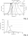
- Fig. 2 is a spectral profile coordination diagram illustrating targeted coordination between a wavelength range of excitation light, a wavelength range of signal light and a detection wavelength range.
- spectral profile 1202 is the spectral profile of excitation light 101 as emitted by light energy exciter 10.
- Spectral profile 1204 is the spectrum of absorption of a fluorophore being detected with use of excitation light 101 having a spectral profile 1202 and spectral profile 1214 is the spectral profile of the emissions signal light 501 caused by the fluorescence of a fluorophore on being excited by excitation light 101.
- Spectral profile 1220 is the transmission profile (detection band) of detector 200 and light sensors 202 according to one example.
- Detector 200 can be configured to detect light in the wavelength range indicated by spectral profile 1220.
- detector 200 is able to detect emissions signal light 501 in the range of wavelengths wherein the spectral profile 1214 of the emissions signal light 501 and the detection band spectral profile 1220 of detector 200 and light sensors 202 intersect.
- Detector 200 can include one or more filters that block excitation light 101 so that detector 200 having light sensors 202 does not detect excitation light 101.
- light guides 214 that guide light from detector surface 206 can comprise filter material so that light guides 214 block light in the wavelength range of excitation light 101.
- Light sensors 202 accordingly can receive emissions signal light 501 radiating from an excited fluorophore but not excitation light 101.
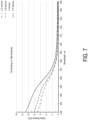
- spectral profile 1304 is a spectral profile of a filter material having a dye that is without (absent) a photon emission quencher commonly used in optical systems under test by excitation illumination in an expected wavelength range of excitation light 101 of system 100.
- spectral profile 1304 illustrates a spectral profile of a filter material under illumination by green excitation light, e.g. according to the excitation light spectral profile 1202 depicted in the spectral profile coordination diagram of Fig. 2 , having a center (peak) wavelength of about 523 nm.
- the filter material having spectral profile characteristics depicted by spectral profile 1304 red shifts with respect to the emission band of excitation light 101 depicted by spectral profile 1202 of the spectral profile coordination diagram of Fig. 2 , meaning that the material exhibits autofluorescence.
- light guides 214 can comprise material having a photon emission quencher.
- a filter material can include dye molecules to provide absorption in a wavelength band of excitation light 101.
- the energy state transition diagram of Fig. 4 depicts energy state transition of a dye without a photon emission quencher. On excitation and after an excitation state relaxation period the dye having the energy state transition characteristics as depicted in the energy state transition diagram of Fig. 4 emits photons on return to a ground state.
- Fig. 5 is an energy state transition diagram depicting energy state transitions of a dye having a photon emission quencher. Referring to the energy state transition diagram of Fig. 5 , the dye having a photon emission quencher on excitation returns to a ground state after an excitation state relaxation period. However, by operation of the photon emission quencher, photons are not released on return to the ground state. Rather phonons are emitted on return to the ground state. The return to ground state is accompanied by the release of thermal energy rather than photons.
- Dyes having the energy state transition characteristics as shown in the energy state transition diagram of Fig. 4 are radiant dyes and dyes having energy state transition characteristics as shown in the energy state transition diagram of Fig. 5 are non-radiant dyes.
- a chemical structure diagram of a dye, according to one example, having a suitable photon emission quencher that quenches photon emissions is shown in (2).
- the chemical structural diagram of (2) illustrates structural characteristics of a metal complex dye that functions as a photon emission quencher to quench photon emissions.
- a metal complex dye can be provided by an octahedral transition metal complex dye as shown in (2).
- the specific metal complex dye shown in (2) includes two dye molecules + chromium ion, and some complexes can include one dye molecule + one chromium (Cr) ion or other metal ion.
- the structure depicted in (2) includes six ligand bonds: O, N and a standard crystal field. According to the structure depicted in (2), there is a photon emission quencher provided by a trivalent Cr transition metal ion. According to one example Cr3 + can provide photon emission quenching functionality.
- Transition metals for use in a metal complex dye herein can include e.g. Scandium, Titanium, Vanadium, Chromium, Manganese, Iron, Cobalt, Nickel, Copper.
- energy levels can be overlapping between the metal ion and a dye molecule.
- a transition metal for use in a metal complex dye can be selected to have an absorption spectral profile overlapping a fluorescence emissions profile of the selected dye so that the transition metal can provide photon emission quenching functionality through the fluorescence emission spectral profile of the selected dye.
- the metal complex dye has an associated proton depicted.
- the counter ion associated to the metal complex dye is formed by absorbing the positive (+) charge specified by the proton of the metal complex dye depicted in the structural diagram of (2) and can be selected according to one example for hydrophobicity performance and UV absorption performance.
- an alkyl amine, a primary amine, a secondary amine, or a tertiary amine may associate with the metal complex dye forming a counter ion, which can include an alkylammonium when associated with the metal complex dye.
- the metal complex dye according to one example may not be particularly soluble in a solution on its own, and so the counter ion can be chosen to increase solubility.
- the counter ion can be selected for hydrophobicity performance in order to promote transparency and visibility of the polymer and/or solvent, and for reducing scattering. For instance, the counter ion can allow for the metal complex dye to be more evenly distributed, enhancing the visibility and transparency, and reducing scattering.
- the counter ion can be selected for UV absorption performance e.g. so that the counter ion does not undesirably contribute to fluorescence.
- absorption of the counter ion can affect the fluorescence characteristics by interfering with the spectrum of the metal dye complex, and can be chosen so as not to have an interfering spectrum.
- a hydrophobic amine can be used as a counter ion.
- a metal complex dye may have no charge, a net positive charge, or may have a net negative charge as well.
- a counter ion associated to the metal complex dye depicted in the structural diagram of (2) can be provided by an alkyl amine.
- a counter ion associated to the metal complex dye depicted in the structural diagram of (2) can be provided by a tertiary amine.
- a nitrogen has three organic substituents.
- a counter ion associated to the metal complex dye depicted in the structural diagram of (2) can be provided by a tertiary alkyl amine.
- a counter ion of appropriate charge can be selected to be associated to the metal complex dye.
- a negatively or positively charged ion can be selected to counteract the net charge of the metal complex dye molecule, and/or adding to the hydrophobicity in some embodiments to allow for the metal complex dye to be incorporated into a solution.
- no counter ion may be necessary in some embodiments.
- the counter ion may include any charged particles, and in some embodiments includes primary, secondary, or tertiary amines. In further embodiments, a quaternary ammonium ion can be selected.
- the counter ion associated to the metal complex dye as depicted in (2) can include an amine, for instance an NR'R"R"', where at least one of the R groups is a chain, straight or branched, with at least four atoms. In some embodiments, there can be at least 10 atoms in the chain.
- the chain can include a long chain, and can include a polymer.
- the chain may be a mostly hydrocarbon group, or could include other moieties, such that the dye can possibly be soluble in any solvent necessary, and the polymer can be soluble in a solvent depending on the functional groups of the polymer.
- the other R groups can be the same or hydrogen, or can comprise a different chain.
- the chain can be according to one example a C4 to C20, including cyclic, chains or rings.
- the counter ion can include more than one type of counter ion. Examples herein recognize that some mixtures of counter ions are convenient for use in solutions where more than one polymer material can be used. That is, some alkyl groups can be different, and the counter ion can include a plurality of counter ions.
- Fig. 6 is an energy state transition diagram illustrating properties of metal complex dyes.
- Fig. 6 is an energy state transition diagram for Cr (CN tBu Ar 3 NC) 3 .
- metal complexes can lead to ultrafast non-radiative (non-autofluorescence) relaxation due to metal centered states being below the metal-2-ligand charge-transfer (MLCT) complex.
- MLCT metal-2-ligand charge-transfer
- the ligand field can be sufficiently weak that metal centered 3d-d excited states can be energetically below the MLCT complex leading to ultrafast excited state.
- Metal complex dyes can exhibit ultrafast excited state depopulation via non-radiative relaxation.
- a metal complex functioning as a photon emission quencher quenches photons so that a return to ground state is accompanied by phonon emission and release of thermal energy rather than photon emission.
- dye molecules in powder form e.g. having photon emission quencher, and according to one example provided by a metal complex dye
- a solvent e.g. having photon emission quencher
- a metal complex dye e.g., a solvent for a solvent
- the liquid can be deposited into a dielectric stack cavity of detector 200 and evaporated to form a filter material comprising a solid dye and polymer matrix wherein dye molecules are suspended within a matrix of polymer binder molecules.
- a filter material for forming light guide 214 can include metal complex dye molecules suspended in a polymer binder matrix as set forth herein.
- a formed filter material including metal complex dye molecules suspended in a polymer binder matrix can exhibit spectral profile characteristics under illumination with excitation light 101 having a center wavelength of about 523 nm as set forth with reference to spectral profile 1404 as shown in the spectral profile diagram of Fig. 3 .
- Providing a matrix of dye molecules with a polymer binder molecule facilitates processability with a range of semiconductor processes e.g. chemical vapor deposition (CVD), spin coating, etching, planarizing, and the like.
- CVD chemical vapor deposition
- spin coating etching
- planarizing planarizing
- a filter material can include a dye having a photon emission quencher and the dye can be a non-radiant dye.
- the photon emission quencher can include chromium (Cr).
- the dye can be a metal complex dye having a photon emission quencher provided by a trivalent Cr transition metal ion.
- the filter material can be provided by matrix having a dye and polymer binder, wherein the dye has a photon emission quencher.
- the filter material can be provided by matrix having a dye and polymer binder, wherein the dye is a metal complex dye.
- the filter material can be provided by a dye suspended in a polymer matrix, wherein the dye has a photon emission quencher.
- the filter material can be provided by a dye suspended in a polymer matrix, wherein the dye is a metal complex dye.
- Fig. 8 there are set forth additional features for increasing a signal to noise ratio of detector 200.
- Fig. 8 there are described features for cancellation (e.g. partial or entire cancellation) of fluorescence range background noise radiation that without the described features would be received into detector 200.
- Cancellation features herein can reduce fluorescence range wavelengths sensed by light sensors 202 not attributable to emissions signal light 501.
- the filter material features set forth in reference to Figs. 3-7 reduce fluorescence range noise by reduction of internal autofluorescence within detector 200.
- detector surface 206 as set forth in connection with Fig. 8 reduce undesirable fluorescence range background noise by cancellation (e.g. partial or entire) fluorescence range light energy incident on detector surface 206.
- the features described with reference to Fig. 3-7 can be implemented independently of the features of Fig. 8 or according to one example in combination with the features of Fig. 8 to address the problem of fluorescence range noise with use of a combination of detector internal ( Figs. 3-7 ) and detector surface ( Fig. 8 ) features.
- detector 200 can be configured so that light energy incident on detector surface 206 can induce electromagnetic fields radiating from detector surface 206 that cancel (e.g. partially or entirely) incoming light energy which would otherwise be transmitted through reaction recess 210. Examples herein recognize that behavior of induced fields radiating from detector surface 206 induced from light rays incident on detector surface 206 can become more controllable and predictable as an index of refraction ratio between a detector surface 206 and fluid within flow cell 282 increases.
- An index of refraction of detector surface 206 can be defined by the index of refraction of the material of passivation layer 258 adjacent flow cell 282 forming the detector surface 206.
- reaction recess 210 can include a dimension "D" provided by the diameter of the reaction recess 210 at a top elevation of reaction recess 210. Examples herein recognize that electromagnetic fields induced by incident light energy incident on reaction recess 210 can cancel incoming light energy in dependence on the dimension "D", where an index of refraction ratio between detector surface 206 and fluid within flow cell 282 is sufficiently high.
- Detector 200 as shown in Fig. 8 can be an integrated circuit detector having structure 260 defining detector surface 206 which can include passivation layer 256 and passivation layer 258.
- passivation layer 258 having detector surface 206 is formed of tantalum pentoxide (Ta2O5) having an index of refraction ⁇ 206 of about 1206 ⁇ 2.13 and where fluid of flow cell 282 is water based and has an index of refraction ⁇ 282 of about ⁇ 282 ⁇ 1.33 the index of refraction ratio ⁇ 206/ ⁇ 282 between a material forming detector surface 206 and a fluid of flow cell 282 is about ⁇ 206/ 1282 ⁇ 1.60.
- Ta2O5 tantalum pentoxide
- passivation layer 258 having detector surface 206 is formed of silicon nitride (SiN) having an index of refraction ⁇ 206 of about ⁇ 206 ⁇ 2.02 and where fluid of flow cell 282 is water based and has an index of refraction ⁇ 282 of about ⁇ 282 ⁇ 1.33 the index of refraction ratio ⁇ 206/ ⁇ 282 between a material forming detector surface 206 and a fluid of flow cell 282 is about ⁇ 206/ 1282 ⁇ 1.52.
- a three-dimensional shape of reaction recess 210 can be cylindrical or frustro-conical in some examples such that a cross-section taken along a horizontal plane that extends into the page of Fig. 8 is substantially circular.
- a longitudinal axis 268 can extend through a geometric center of the cross-section.
- Examples herein recognize that for a detector surface 206 as set forth in Fig. 8 having a reaction recess 210 (nanowell) with the dimension D and with an index of refraction ratio ⁇ 206/ ⁇ 282 suitably high there is a critical wavelength ⁇ c wherein wavelengths shorter than the critical wavelength ⁇ c are transmitted into an interior of reaction recess 210 and detector 200 and wherein wavelengths longer than the critical wavelength ⁇ c are cancelled (e.g. partially cancelled or entirely cancelled) by detector surface 206 having reaction recess 210. Examples herein further recognize that the described critical wavelength ⁇ c is in dependence of the dimension D so that the dimension D can be controlled to tune the critical dimension ⁇ c to a desired value.
- the critical wavelength ⁇ c can be increased by increasing the dimension D and the critical wavelength ⁇ c can be decreased by decreasing the dimension D.
- light rays incident on detector surface 206 may induce electromagnetic fields radiating from detector surface 206 that cancel (e.g. partially or entirely) incoming light energy which would otherwise be transmitted through reaction recess 210.
- Light energy cancellation features can be advantageously incorporated into the design of detector surface 206.
- the dimension D can be selected to establish the critical wavelength ⁇ c so that wavelengths at about the center (peak) wavelength ⁇ a of excitation light 101 and shorter are transmitted through reaction recess 210 and into detector 200 and further so that wavelengths of about the shortest detection band wavelength ⁇ b and longer are cancelled by detector surface 206.
- Transmission of wavelengths at about the center (peak) wavelength ⁇ a of excitation light 101 and shorter can assure that fluorophores are properly excited according to the design of system 100 and cancellation of wavelengths of about the shortest detection band wavelength ⁇ b and longer can increase a signal to noise ratio of detector 200.
- ⁇ c can be tuned in dependence on D
- the precise relationship between D and cancellation effects in dependence thereon can vary depending on materials, configuration (including light energy exciter 10 configuration), and process control parameters of a particularly fabricated system 100. Notwithstanding, information of the relationship between the dimension D and a cancellation effect in dependence thereon for a particular design of detector 200 can be determined by experimentation.
- one or more test sample detectors according to detector 200 can be fabricated and subject to test.
- the test can include testing for transmission of excitation light 101 by reaction recess 210.
- the one or more transmission criterion can be e.g. that a threshold amount (e.g. 90 percent, 100 percent) of maximum energy excitation light 100 is transmitted through reaction recess 210.
- detector 200 according to a production design can be provided.
- the dimension D can be provided to establish a critical wavelength ⁇ c so that ⁇ c is within a range of wavelengths of between about ⁇ a and about ⁇ b, wherein wavelengths shorter than ⁇ c are transmitted by reaction recess 210 and wherein wavelengths longer than ⁇ c are cancelled by reaction recess 210, wherein ⁇ a is the center wavelength of excitation light 101 and wherein ⁇ b is the shortest detection band wavelength of the sensor array 201.
- excitation light 101 can have a center (peak) wavelength of about 523 nm ( ⁇ a), and detector 200 with light sensors 202 can have a detection band commencing at about 580 nm (shortest detection band wavelength ⁇ b).
- reaction recess 210 configured to have a suitable index of refraction, can be dimensioned to permit entry of incident light energy at wavelengths of about 523 nm and shorter and can be dimensioned to cancel incident light energy at wavelengths of about 580 nm and longer.
- the detector surface 206 can be dimensioned to permit entry of incident light energy at wavelengths of about 523 nm and shorter and can be dimensioned to cancel incident light energy at wavelengths of about 580 nm and longer.
- a method including subjecting a test sample detector according to detector 200 (having a structure 260 defining detector surface 206) to determine information that specifies a relationship between a dimension e.g. D of detector surface 206 and an electromagnetic field cancellation effect (e.g. including information such dc, de and/or other information relating D to ⁇ c ) and wherein the fabricating the structure 260 defining a detector surface 206 includes dimensioning, using the determined information, a reaction recess 210 of the detector surface 206 to transmit excitation light 101 in an excitation wavelength band of excitation light 101 (including at the center (peak) wavelength ⁇ a) and to cancel light energy incident on the detector surface 206 in a detection band of the light sensor array 201.
- a three-dimensional shape of reaction recess 210 can be cylindrical or frustro-conical in some examples such that a cross-section taken along a horizontal plane that extends into the page of Fig. 8 is circular.
- a longitudinal axis 268 can extend through a geometric center of the cross-section.
- the cross-section can be square-shaped or octagonal.
- shield structure 250 can have a thickness of from about 100 nm to about 600 nm
- passivation layer 256 can have a thickness of from about 100 nm to about 600 nm
- passivation layer 256 can have a thickness of from about 50 nm to about 500 nm
- aperture 252 can have a diameter of from about 700 nm to about 1.5 ⁇ m
- reaction recess 210 if present can have a height H of from about 50 nm to about 500 nm.
- Figs. 9 and 10 illustrate further details of an example of detector 200 having one or more fluorescence range noise reducing features as set forth herein.
- a detector surface 206 for supporting biological or chemical substances; a sensor array 201 comprising light sensors 202, and circuitry 246 to transmit data signals based on photons detected by the light sensors 202; a guide array 213 comprising light guides 214; wherein light guides 214 of the guide array 213 receive excitation light 101 and emissions signal light 501 from the detector surface 206, wherein the light guides 214 extend toward respective light sensors 202 of the sensor array 201 and comprise filter material that blocks the excitation light 101 and permits emissions signal light 501 radiating from fluorescing fluorophores to propagate toward the respective light sensors 202, wherein the detector surface includes a reaction recess 210, the reaction recess comprising an index of refraction and a dimension to cancel background light energy incident on the detector surface in a detection band of the sensor array 201.
- Detector 200 can include a sensor array 201 of light sensors 202, a guide array 213 of light guides 214, and a reaction array 209 of reaction recesses 210.
- the components are arranged such that each light sensor 202 aligns with a single light guide 214 and a single reaction recess 210.
- a single light sensor 202 can receive photons through more than one light guide 214.
- array does not necessarily include each and every item of a certain type that the detector can have.
- the sensor array of light source may not include each and every light sensor of detector 200.
- the guide array 213 may not include each and every light guide of detector 200.
- the reaction array 209 may not include each and every reaction recess 210 of detector 200.
- the term "array" may or may not include all such items of detector 200.
- flow cell 282 is defined by sidewall 284 and a flow cover 288 that is supported by the sidewall 284 and other sidewalls (not shown).
- the sidewalls are coupled to the detector surface 206 and extend between the flow cover 288 and the detector surface 206.
- the sidewalls are formed from a curable adhesive layer that bonds the flow cover 288 to detector 200.
- the flow cell 282 can include a height H1.
- the height H1 can be between about 50-400 ⁇ m or, more particularly, about 80-200 ⁇ m.
- the flow cover 288 can include a material that is light transmissive to excitation light 101 propagating from an exterior of the detector assembly 20 into the flow cell 282.
- the flow cover 288 can define inlet and outlet ports 289, 290 that are configured to fluidically engage other ports (not shown).
- the other ports can be from a cartridge (not shown) or a workstation (not shown).
- Detector 200 has a detector surface 206 that can be functionalized (e.g. chemically or physically modified in a suitable manner for conducting designated reactions).
- the detector surface 206 can be functionalized and can include a plurality of reaction sites having one or more biomolecules immobilized thereto.
- the detector surface 206 can have a reaction array 209 of reaction recesses 210.
- Each of the reaction recesses 210 can include one or more of the reaction sites.
- the reaction recesses 210 can be defined by, for example, an indent or change in depth along the detector surface 206. In other examples, the detector surface 206 can be planar.
- Fig. 10 is an enlarged cross-section of detector 200 showing various features in greater detail. More specifically, Fig. 10 shows a single light sensor 202, a single light guide 214 for directing emissions signal light 501 toward the light sensor 202, and associated circuitry 246 for transmitting signals based on emissions signal light 501 (e.g. photons) detected by the light sensor 202. It is understood that the other light sensors 202 of the sensor array 201 ( Fig. 9 ) and associated components can be configured in an identical or similar manner. It is also understood, however, the detector 200 is not required to be manufactured identically or uniformly throughout. Instead, one or more light sensors 202 and/or associated components can be manufactured differently or have different relationships with respect to one another.
- the circuitry 246 can include interconnected conductive elements (e.g. conductors, traces, vias, interconnects, etc.) that are capable of conducting electrical current, such as the transmission of data signals that are based on detected photons.
- Detector 200 comprises an integrated circuit having a planar array of the light sensors 202.
- the circuitry 246 formed within detector 200 can be configured for at least one of read out signals from light sensors 202 after an exposure period (integration period) in which charge accumulates on light sensor 202, signal amplification, digitization, storage, and processing.
- the circuitry 246 can collect and analyze the detected emissions signal light 501 and generate data signals for communicating detection data to a bioassay system.
- the circuitry 246 can also perform additional analog and/or digital signal processing in detector 200.
- Light sensors 202 can be electrically coupled to circuitry 246 through gates 241-243.
- Detector 200 can be provided by a solid-state integrated circuit detector such as a CMOS integrated circuit detector or a CCD integrated circuit detector.
- Detector 200 according to one example can be an integrated circuit chip manufactured using integrated circuit manufacturing processes such as complementary metal oxide semiconductor (CMOS) fabrication processes.
- CMOS complementary metal oxide semiconductor
- the resolution of the sensor array 201 defined by light sensors 202 can be greater than about 0.5 megapixels (Mpixels). In more specific examples, the resolution can be greater than about 5 Mpixels and, more particularly, greater than about 14 Mpixels.
- Detector 200 can include a plurality of stacked layers 231-237 including a sensor layer 231, which can be a silicon layer.
- the stacked layers can include a plurality of dielectric layers 232-237.
- each of the dielectric layers 232-237 includes metallic elements (e.g. W (tungsten), Cu (copper), or Al (aluminum)) and dielectric material, e.g. SiO2.
- metallic elements and dielectric material can be used, such as those suitable for integrated circuit manufacturing.
- one or more of the dielectric layers 232-237 can include only dielectric material, such as one or more layers of SiO2.
- the dielectric layers 232-237 can include metallization layers that are labeled as layers M1-M5 in Fig. 10 .
- the metallization layers, M1-M5 can be configured to form at least a portion of the circuitry 246.
- detector 200 includes a shield structure 250 having one or more layers that extend throughout an area above metallization layer M5.
- the shield structure 250 can include a material that is configured to block, reflect, and/or significantly attenuate the light signals that are propagating from the flow cell 282.
- the light signals can be the excitation light 101 and/or emissions signal light 501.
- the shield structure 250 can comprise tungsten (W).
- the excitation light 101 may have a center (peak) wavelength of about 523 nm and emissions signal light 501 can include wavelengths of about 570 nm and longer ( Fig. 2 ).
- shield structure 250 can include an aperture 252 therethrough.
- the shield structure 250 can include an array of such apertures 252.
- Aperture 252 is dimensioned to allow signal emission light to propagate to light guide 214.
- Detector 200 can also include a passivation layer 256 that extends along the shield structure 250 and across the apertures 252.
- Detector 200 can also include a passivation layer 258 comprising detector surface 206 that extends along passivation layer 256 and across the apertures 252.
- Shield structure 250 can extend over the apertures 252 thereby directly or indirectly covering the apertures 252.
- Passivation layer 256 and passivation layer 258 can be configured to protect lower elevation layers and the shield structure 250 from the fluidic environment of the flow cell 282.
- passivation layer 256 is formed of SiN or similar.
- passivation layer 258 is formed of tantalum pentoxide (Ta2O5) or similar.
- Structure 260 having passivation layer 256 and passivation layer 258 can define detector surface 206 having reaction recesses 210.
- Structure 260 defining detector surface 206 can have any number of layers such as one to N layer.
- Structure 260 can define a solid surface (i.e., the detector surface 206) that permits biomolecules or other analytes-of-interest to be immobilized thereon.
- each of the reaction sites of a reaction recess 210 can include a cluster of biomolecules that are immobilized to the detector surface 206 of the passivation layer 258.
- the passivation layer 258 can be formed from a material that permits the reaction sites of reaction recesses 210 to be immobilized thereto.
- the passivation layer 258 can also comprise a material that is at least transparent to a desired fluorescent light. Passivation layer 258 can be physically or chemically modified to facilitate immobilizing the biomolecules and/or to facilitate detection of the emissions signal light 501.
- reaction recess 210 can be aligned with and formed directly over light guide 214. According to one example each of reaction recess 210 and light guide 214 can have geometric centers centered on longitudinal axis 268.
- shield structure 250 can have a thickness of from about 100 nm to about 600 nm
- passivation layer 256 can have a thickness of from about 100 nm to about 600 nm
- passivation layer 256 can have a thickness of from about 50 nm to about 500 nm
- aperture 252 can have a diameter of from about 700 nm to about 1.5 um
- reaction recess 210 if present can have a height of from about 50 nm to about 500 nm.
- a cavity defined by sidewalls 254 can be formed the dielectric stack defined by dielectric layers 232-237 prior to the passivation layer 256 being deposited along the shield structure 250, and prior to a depositing of shield structure 250 a cavity defined by sidewalls 254 can be formed the dielectric stack defined by dielectric layers 232-237.
- the dielectric stack defined by dielectric layers 232-237 can be etched to form an array of the cavities defined by sidewalls 254, wherein one cavity is formed for each light sensor 202 of light sensor array 201.
- a cavity defined by sidewalls 254 is a vertically elongated space that extends from proximate the aperture 252 toward the light sensor 202.
- the cavity can extend vertically along longitudinal axis 268.
- a three-dimensional shape of cavity defined by sidewalls 254 can be cylindrical or frustro-conical in some examples such that a cross-section taken along a horizontal plane that extends into the page of Fig. 10 is circular.
- the longitudinal axis 268 can extend through a geometric center of the cross-section.
- the cross-section can be square-shaped or octagonal.
- the longitudinal axis 268 which is the longitudinal axis of light guide 214 can extend through a geometric center of light sensor 202 and reaction recess 210.
- the filter material defining light guide 214 can be deposited within the cavity defined by sidewalls 254 after the cavity defined by sidewalls 254 is formed.
- dye molecules in powder form e.g. having photon emission quencher
- a solvent e.g., ethanol
- the dye molecules in powder form can be metal complex dye particles.
- the homogeneous liquid matrix can be deposited into a dielectric stack cavity of detector 200 and evaporated to form a filter material comprising a solid dye and polymer matrix wherein dye molecules are suspended within a matrix of polymer binder molecules.
- the homogeneous polymer binder and dye matrix filter material can be deposited into the cavity defined by sidewalls 254, using e.g. chemical vapor deposition (CVD) physical vapor deposition (PVD).
- the depositing can be performed to overfill the cavity defined by sidewalls 254 with filter material and then subject to patterning such as by planarization or etching to reduce the elevation of the filter material defining light guide 214.
- a filter material for forming light guide 214 can include metal complex dye molecules suspended in a polymer binder molecule matrix.
- the filter material can form (e.g. after curing) a light guide 214.
- the light guide 214 can be configured to block the excitation light 101 and permit emissions signal light 501 ( Fig. 1 ) to propagate therethrough toward the corresponding light sensor 202.
- the light guide 214 can be formed of filter material described in reference to Figs. 2-7 herein.
- the filter material can include a homogeneous matrix of dye and polymer binder, wherein the dye can include a photon emission quencher and according to one example is provided by a metal complex dye.
- the dye and polymer matrix according to one example can include a weight concentration in the range of from about 70:30 dye to polymer to about 90:10 dye to polymer.
- the filter material mixture can have a molecule ratio of about 1 dye molecule to about 100 polymer molecules.
- the light guide 214 can be configured relative to surrounding material of the dielectric stack defined by dielectric layers 231-237 to form a light-guiding structure.
- the light guide 214 can have a refractive index of at least about 2.0 so that light energy propagating through light guide is reflected at an interface between light guide 214 and the surrounding dielectric stack defined by dielectric layers 231-237.
- the light guide 214 is configured such that the optical density (OD) or absorbance of the excitation light 101 is at least about 4 OD.
- the filter material can be selected and the light guide 214 can be dimensioned to achieve at least 4 OD.
- the light guide 214 can be configured to achieve at least about 5 OD or at least about 6 OD.
- the light guide 214 can be configured to achieve at least about 5 OD or at least about 6 OD.
- Other features of the detector 200 can be configured to reduce electrical and optical crosstalk.
Landscapes
- Health & Medical Sciences (AREA)
- Physics & Mathematics (AREA)
- Life Sciences & Earth Sciences (AREA)
- Immunology (AREA)
- Chemical & Material Sciences (AREA)
- General Physics & Mathematics (AREA)
- Pathology (AREA)
- Analytical Chemistry (AREA)
- Biochemistry (AREA)
- General Health & Medical Sciences (AREA)
- Nuclear Medicine, Radiotherapy & Molecular Imaging (AREA)
- Engineering & Computer Science (AREA)
- Optics & Photonics (AREA)
- Biomedical Technology (AREA)
- Molecular Biology (AREA)
- Hematology (AREA)
- Urology & Nephrology (AREA)
- Cell Biology (AREA)
- Microbiology (AREA)
- Biotechnology (AREA)
- Food Science & Technology (AREA)
- Medicinal Chemistry (AREA)
- Chemical Kinetics & Catalysis (AREA)
- Investigating, Analyzing Materials By Fluorescence Or Luminescence (AREA)
- Investigating Or Analysing Materials By The Use Of Chemical Reactions (AREA)
- Measurement Of The Respiration, Hearing Ability, Form, And Blood Characteristics Of Living Organisms (AREA)
- Optical Measuring Cells (AREA)
- Optical Filters (AREA)
Applications Claiming Priority (4)
| Application Number | Priority Date | Filing Date | Title |
|---|---|---|---|
| US201762611464P | 2017-12-28 | 2017-12-28 | |
| US201862644804P | 2018-03-19 | 2018-03-19 | |
| EP18896064.5A EP3732468B1 (en) | 2017-12-28 | 2018-11-30 | Device with reduced fluorescence range noise and method |
| PCT/US2018/063395 WO2019133182A1 (en) | 2017-12-28 | 2018-11-30 | Detector with reduced fluorescence range noise |
Related Parent Applications (1)
| Application Number | Title | Priority Date | Filing Date |
|---|---|---|---|
| EP18896064.5A Division EP3732468B1 (en) | 2017-12-28 | 2018-11-30 | Device with reduced fluorescence range noise and method |
Publications (3)
| Publication Number | Publication Date |
|---|---|
| EP3978908A1 EP3978908A1 (en) | 2022-04-06 |
| EP3978908B1 true EP3978908B1 (en) | 2025-05-07 |
| EP3978908C0 EP3978908C0 (en) | 2025-05-07 |
Family
ID=67058128
Family Applications (2)
| Application Number | Title | Priority Date | Filing Date |
|---|---|---|---|
| EP21208877.7A Active EP3978908B1 (en) | 2017-12-28 | 2018-11-30 | Device with reduced fluorescence range noise and method |
| EP18896064.5A Active EP3732468B1 (en) | 2017-12-28 | 2018-11-30 | Device with reduced fluorescence range noise and method |
Family Applications After (1)
| Application Number | Title | Priority Date | Filing Date |
|---|---|---|---|
| EP18896064.5A Active EP3732468B1 (en) | 2017-12-28 | 2018-11-30 | Device with reduced fluorescence range noise and method |
Country Status (25)
| Country | Link |
|---|---|
| US (6) | US10551317B2 (da) |
| EP (2) | EP3978908B1 (da) |
| JP (1) | JP6827570B2 (da) |
| KR (2) | KR102261632B1 (da) |
| CN (3) | CN109975255B (da) |
| AU (2) | AU2018397465A1 (da) |
| BR (1) | BR112019028286B1 (da) |
| CA (2) | CA3191105C (da) |
| CL (1) | CL2019003784A1 (da) |
| CO (1) | CO2019014476A2 (da) |
| CR (1) | CR20190584A (da) |
| DK (1) | DK3732468T3 (da) |
| ES (1) | ES2906809T3 (da) |
| IL (1) | IL271293B (da) |
| MX (1) | MX381250B (da) |
| MY (1) | MY194752A (da) |
| NZ (1) | NZ778619A (da) |
| PE (1) | PE20200893A1 (da) |
| PH (1) | PH12019502900A1 (da) |
| RU (1) | RU2738311C1 (da) |
| SA (1) | SA519410862B1 (da) |
| SG (1) | SG11201912255RA (da) |
| TW (1) | TWI698638B (da) |
| WO (1) | WO2019133182A1 (da) |
| ZA (1) | ZA201908274B (da) |
Families Citing this family (13)
| Publication number | Priority date | Publication date | Assignee | Title |
|---|---|---|---|---|
| US8906320B1 (en) | 2012-04-16 | 2014-12-09 | Illumina, Inc. | Biosensors for biological or chemical analysis and systems and methods for same |
| NL2020625B1 (en) * | 2017-12-22 | 2019-07-02 | Illumina Inc | Two-filter light detection devices and methods of manufacturing same |
| US10861829B2 (en) | 2017-12-26 | 2020-12-08 | Illumina, Inc. | Sensor system |
| TWI698638B (zh) * | 2017-12-28 | 2020-07-11 | 美商伊路米納有限公司 | 具有降低的螢光範圍雜訊的檢測器以及用於降低螢光範圍雜訊的方法 |
| EP3850336A4 (en) | 2018-09-14 | 2022-02-09 | Illumina, Inc. | FLOW CELLS AND RELATED PROCEDURES |
| TWI688088B (zh) * | 2019-07-24 | 2020-03-11 | 晶相光電股份有限公司 | 影像感測裝置及影像感測系統 |
| US11105745B2 (en) * | 2019-10-10 | 2021-08-31 | Visera Technologies Company Limited | Biosensor |
| US11557625B2 (en) * | 2020-04-20 | 2023-01-17 | Omnivision Technologies, Inc. | Image sensors with embedded wells for accommodating light emitters |
| US20210379578A1 (en) * | 2020-06-04 | 2021-12-09 | Illumina, Inc. | Apparatus with a sensor having an active surface |
| CN112924427B (zh) * | 2021-02-02 | 2022-07-08 | 中国农业科学院特产研究所 | 一种消除植物组织自体荧光的方法 |
| GB2607603A (en) * | 2021-06-08 | 2022-12-14 | Spectrum Logic Ltd | Imaging apparatus |
| CN118339481A (zh) * | 2021-11-15 | 2024-07-12 | 深圳帧观德芯科技有限公司 | 用于x射线荧光成像的装置和方法 |
| CN118215861A (zh) * | 2021-11-16 | 2024-06-18 | 深圳帧观德芯科技有限公司 | 具有屏蔽电子器件层的图像传感器 |
Family Cites Families (32)
| Publication number | Priority date | Publication date | Assignee | Title |
|---|---|---|---|---|
| JP3463867B2 (ja) | 1999-09-24 | 2003-11-05 | 富士電機株式会社 | 蛍光色変換膜、それを用いた蛍光色変換フィルターおよび該蛍光色変換フィルターを具備した有機発光素子 |
| JP2002022935A (ja) * | 2000-07-06 | 2002-01-23 | Fuji Photo Film Co Ltd | 光学フィルター |
| US7081991B2 (en) * | 2003-03-14 | 2006-07-25 | Rockwell Collins, Inc. | Dye-based filter |
| US7245079B2 (en) * | 2003-05-28 | 2007-07-17 | Solutia Incorporated | Plasma display panel filters comprising multiple layers |
| CN101393362B (zh) | 2003-07-14 | 2012-04-11 | 株式会社日立显示器 | 显示装置 |
| JP4701739B2 (ja) * | 2005-02-17 | 2011-06-15 | パナソニック株式会社 | 蛍光測定装置 |
| FR2892196B1 (fr) * | 2005-10-18 | 2008-06-20 | Genewave Soc Par Actions Simpl | Procede de fabrication d'un biocapteur a detection integree |
| US7226831B1 (en) | 2005-12-27 | 2007-06-05 | Intel Corporation | Device with scavenging spacer layer |
| US8637436B2 (en) * | 2006-08-24 | 2014-01-28 | California Institute Of Technology | Integrated semiconductor bioarray |
| WO2007143669A2 (en) | 2006-06-05 | 2007-12-13 | California Institute Of Technology | Real time micro arrays |
| JP4909656B2 (ja) * | 2006-06-26 | 2012-04-04 | 富士フイルム株式会社 | Dna解析用デバイス、dna解析装置 |
| JP5376963B2 (ja) * | 2008-01-25 | 2013-12-25 | 富士フイルム株式会社 | 光電変換素子及び撮像素子 |
| EP2331934B1 (en) * | 2008-09-16 | 2020-01-01 | Pacific Biosciences of California, Inc. | Analytic device including a zero mode waveguide substrate |
| US9382450B2 (en) * | 2009-01-20 | 2016-07-05 | Cabot Corporation | Compositions comprising silane modified metal oxides |
| EP2221606A3 (en) * | 2009-02-11 | 2012-06-06 | Samsung Electronics Co., Ltd. | Integrated bio-chip and method of fabricating the integrated bio-chip |
| EP3460458B1 (en) | 2010-02-19 | 2021-08-11 | Pacific Biosciences of California, Inc. | A method for nucleic acid sequencing |
| CN102906239B (zh) * | 2010-05-18 | 2015-09-09 | 美利肯公司 | 荧光增白剂及含有其的组合物 |
| KR102130856B1 (ko) * | 2011-09-30 | 2020-07-08 | 라이프 테크놀로지스 코포레이션 | 생물학적 분석을 위한 광학 시스템 및 방법 |
| KR101359379B1 (ko) | 2012-03-28 | 2014-02-07 | 광주과학기술원 | Cmos 이미지 센서의 픽셀 분석을 이용한 고감도 바이오센서 |
| US8906320B1 (en) | 2012-04-16 | 2014-12-09 | Illumina, Inc. | Biosensors for biological or chemical analysis and systems and methods for same |
| EP2728343A1 (en) * | 2012-11-06 | 2014-05-07 | Technische Universität Graz | Optical probe for quantitatively determining an analyte |
| KR102074945B1 (ko) * | 2013-03-14 | 2020-02-07 | 삼성전자 주식회사 | 광 바이오센서 및 바이오 센싱 시스템 |
| RU133932U1 (ru) * | 2013-03-15 | 2013-10-27 | Федеральное государственное унитарное предприятие Государственный научно-исследовательский институт биологического приборостроения (ФГУП "ГосНИИБП)" | Устройство для считывания люминесцентных сигналов с поверхности биочипов |
| CA2932916C (en) * | 2013-12-10 | 2021-12-07 | Illumina, Inc. | Biosensors for biological or chemical analysis and methods of manufacturing the same |
| US10174363B2 (en) * | 2015-05-20 | 2019-01-08 | Quantum-Si Incorporated | Methods for nucleic acid sequencing |
| TWI692633B (zh) | 2014-08-27 | 2020-05-01 | 美商加州太平洋生物科學公司 | 整合式分析裝置之陣列 |
| TWI571626B (zh) | 2015-07-15 | 2017-02-21 | 力晶科技股份有限公司 | 具有奈米腔的集成生物感測器及其製作方法 |
| US10488639B2 (en) | 2015-10-08 | 2019-11-26 | Visera Technologies Company Limited | Detection device for specimens |
| WO2017188441A1 (ja) * | 2016-04-28 | 2017-11-02 | 凸版印刷株式会社 | 解析デバイス、解析キット、及び解析システム |
| JP2018093052A (ja) * | 2016-12-02 | 2018-06-14 | ソニーセミコンダクタソリューションズ株式会社 | 固体撮像素子およびその製造方法、並びに電子機器 |
| CN109425591B (zh) * | 2017-08-31 | 2021-06-25 | 清华大学 | 一种一维纳米材料的观测方法 |
| TWI698638B (zh) * | 2017-12-28 | 2020-07-11 | 美商伊路米納有限公司 | 具有降低的螢光範圍雜訊的檢測器以及用於降低螢光範圍雜訊的方法 |
-
2018
- 2018-11-08 TW TW107139669A patent/TWI698638B/zh active
- 2018-11-30 NZ NZ778619A patent/NZ778619A/en unknown
- 2018-11-30 WO PCT/US2018/063395 patent/WO2019133182A1/en not_active Ceased
- 2018-11-30 PE PE2019002657A patent/PE20200893A1/es unknown
- 2018-11-30 SG SG11201912255RA patent/SG11201912255RA/en unknown
- 2018-11-30 KR KR1020197038418A patent/KR102261632B1/ko active Active
- 2018-11-30 ES ES18896064T patent/ES2906809T3/es active Active
- 2018-11-30 CA CA3191105A patent/CA3191105C/en active Active
- 2018-11-30 EP EP21208877.7A patent/EP3978908B1/en active Active
- 2018-11-30 CR CR20190584A patent/CR20190584A/es unknown
- 2018-11-30 MY MYPI2019007724A patent/MY194752A/en unknown
- 2018-11-30 CA CA3067249A patent/CA3067249C/en active Active
- 2018-11-30 RU RU2019141067A patent/RU2738311C1/ru active
- 2018-11-30 BR BR112019028286-6A patent/BR112019028286B1/pt active IP Right Grant
- 2018-11-30 AU AU2018397465A patent/AU2018397465A1/en not_active Abandoned
- 2018-11-30 KR KR1020217016363A patent/KR102583715B1/ko active Active
- 2018-11-30 JP JP2019571670A patent/JP6827570B2/ja active Active
- 2018-11-30 DK DK18896064.5T patent/DK3732468T3/da active
- 2018-11-30 EP EP18896064.5A patent/EP3732468B1/en active Active
- 2018-11-30 MX MX2019015855A patent/MX381250B/es unknown
- 2018-11-30 US US16/206,564 patent/US10551317B2/en active Active
- 2018-12-18 CN CN201811549746.2A patent/CN109975255B/zh active Active
- 2018-12-18 CN CN202210468525.2A patent/CN115078317B/zh active Active
- 2018-12-18 CN CN201822132123.7U patent/CN209624391U/zh not_active Expired - Fee Related
-
2019
- 2019-12-10 IL IL271293A patent/IL271293B/en active IP Right Grant
- 2019-12-11 ZA ZA2019/08274A patent/ZA201908274B/en unknown
- 2019-12-19 SA SA519410862A patent/SA519410862B1/ar unknown
- 2019-12-20 CO CONC2019/0014476A patent/CO2019014476A2/es unknown
- 2019-12-20 PH PH12019502900A patent/PH12019502900A1/en unknown
- 2019-12-20 CL CL2019003784A patent/CL2019003784A1/es unknown
-
2020
- 2020-01-31 US US16/778,935 patent/US10883937B2/en active Active
- 2020-09-22 US US16/948,524 patent/US11333604B2/en active Active
-
2021
- 2021-05-21 AU AU2021203297A patent/AU2021203297B2/en active Active
-
2022
- 2022-05-02 US US17/734,953 patent/US11852586B2/en active Active
-
2023
- 2023-11-17 US US18/512,284 patent/US12123833B2/en active Active
-
2024
- 2024-10-18 US US18/919,506 patent/US20250044228A1/en active Pending
Also Published As
Similar Documents
| Publication | Publication Date | Title |
|---|---|---|
| US12123833B2 (en) | Detector with reduced fluorescence range noise | |
| EP3133386B1 (en) | Sensing module and sensing method | |
| HK40080478A (en) | Detector with reduced fluorescence range noise | |
| NZ759983B2 (en) | Detector with reduced fluorescence range noise | |
| HK40007477A (en) | Detector with reduced fluorescence range noise | |
| HK40007477B (en) | Detector with reduced fluorescence range noise | |
| RU2819048C1 (ru) | Детектор с уменьшенным шумом в диапазоне флуоресценции |
Legal Events
| Date | Code | Title | Description |
|---|---|---|---|
| PUAI | Public reference made under article 153(3) epc to a published international application that has entered the european phase |
Free format text: ORIGINAL CODE: 0009012 |
|
| STAA | Information on the status of an ep patent application or granted ep patent |
Free format text: STATUS: THE APPLICATION HAS BEEN PUBLISHED |
|
| AC | Divisional application: reference to earlier application |
Ref document number: 3732468 Country of ref document: EP Kind code of ref document: P |
|
| AK | Designated contracting states |
Kind code of ref document: A1 Designated state(s): AL AT BE BG CH CY CZ DE DK EE ES FI FR GB GR HR HU IE IS IT LI LT LU LV MC MK MT NL NO PL PT RO RS SE SI SK SM TR |
|
| STAA | Information on the status of an ep patent application or granted ep patent |
Free format text: STATUS: REQUEST FOR EXAMINATION WAS MADE |
|
| 17P | Request for examination filed |
Effective date: 20221004 |
|
| RBV | Designated contracting states (corrected) |
Designated state(s): AL AT BE BG CH CY CZ DE DK EE ES FI FR GB GR HR HU IE IS IT LI LT LU LV MC MK MT NL NO PL PT RO RS SE SI SK SM TR |
|
| GRAP | Despatch of communication of intention to grant a patent |
Free format text: ORIGINAL CODE: EPIDOSNIGR1 |
|
| STAA | Information on the status of an ep patent application or granted ep patent |
Free format text: STATUS: GRANT OF PATENT IS INTENDED |
|
| RIC1 | Information provided on ipc code assigned before grant |
Ipc: G02B 19/00 20060101ALN20241114BHEP Ipc: H01L 27/146 20060101ALI20241114BHEP Ipc: G02B 5/22 20060101ALI20241114BHEP Ipc: G01N 21/64 20060101AFI20241114BHEP |
|
| RIC1 | Information provided on ipc code assigned before grant |
Ipc: G02B 19/00 20060101ALN20241120BHEP Ipc: H01L 27/146 20060101ALI20241120BHEP Ipc: G02B 5/22 20060101ALI20241120BHEP Ipc: G01N 21/64 20060101AFI20241120BHEP |
|
| INTG | Intention to grant announced |
Effective date: 20241205 |
|
| GRAS | Grant fee paid |
Free format text: ORIGINAL CODE: EPIDOSNIGR3 |
|
| GRAA | (expected) grant |
Free format text: ORIGINAL CODE: 0009210 |
|
| STAA | Information on the status of an ep patent application or granted ep patent |
Free format text: STATUS: THE PATENT HAS BEEN GRANTED |
|
| AC | Divisional application: reference to earlier application |
Ref document number: 3732468 Country of ref document: EP Kind code of ref document: P |
|
| AK | Designated contracting states |
Kind code of ref document: B1 Designated state(s): AL AT BE BG CH CY CZ DE DK EE ES FI FR GB GR HR HU IE IS IT LI LT LU LV MC MK MT NL NO PL PT RO RS SE SI SK SM TR |
|
| REG | Reference to a national code |
Ref country code: GB Ref legal event code: FG4D |
|
| REG | Reference to a national code |
Ref country code: CH Ref legal event code: EP |
|
| REG | Reference to a national code |
Ref country code: DE Ref legal event code: R096 Ref document number: 602018081847 Country of ref document: DE |
|
| REG | Reference to a national code |
Ref country code: IE Ref legal event code: FG4D |
|
| U01 | Request for unitary effect filed |
Effective date: 20250519 |
|
| U07 | Unitary effect registered |
Designated state(s): AT BE BG DE DK EE FI FR IT LT LU LV MT NL PT RO SE SI Effective date: 20250523 |
|
| PG25 | Lapsed in a contracting state [announced via postgrant information from national office to epo] |
Ref country code: ES Free format text: LAPSE BECAUSE OF FAILURE TO SUBMIT A TRANSLATION OF THE DESCRIPTION OR TO PAY THE FEE WITHIN THE PRESCRIBED TIME-LIMIT Effective date: 20250507 |
|
| PG25 | Lapsed in a contracting state [announced via postgrant information from national office to epo] |
Ref country code: NO Free format text: LAPSE BECAUSE OF FAILURE TO SUBMIT A TRANSLATION OF THE DESCRIPTION OR TO PAY THE FEE WITHIN THE PRESCRIBED TIME-LIMIT Effective date: 20250807 Ref country code: GR Free format text: LAPSE BECAUSE OF FAILURE TO SUBMIT A TRANSLATION OF THE DESCRIPTION OR TO PAY THE FEE WITHIN THE PRESCRIBED TIME-LIMIT Effective date: 20250808 |
|
| PG25 | Lapsed in a contracting state [announced via postgrant information from national office to epo] |
Ref country code: PL Free format text: LAPSE BECAUSE OF FAILURE TO SUBMIT A TRANSLATION OF THE DESCRIPTION OR TO PAY THE FEE WITHIN THE PRESCRIBED TIME-LIMIT Effective date: 20250507 |
|
| PG25 | Lapsed in a contracting state [announced via postgrant information from national office to epo] |
Ref country code: HR Free format text: LAPSE BECAUSE OF FAILURE TO SUBMIT A TRANSLATION OF THE DESCRIPTION OR TO PAY THE FEE WITHIN THE PRESCRIBED TIME-LIMIT Effective date: 20250507 |
|
| PG25 | Lapsed in a contracting state [announced via postgrant information from national office to epo] |
Ref country code: RS Free format text: LAPSE BECAUSE OF FAILURE TO SUBMIT A TRANSLATION OF THE DESCRIPTION OR TO PAY THE FEE WITHIN THE PRESCRIBED TIME-LIMIT Effective date: 20250807 |
|
| PG25 | Lapsed in a contracting state [announced via postgrant information from national office to epo] |
Ref country code: IS Free format text: LAPSE BECAUSE OF FAILURE TO SUBMIT A TRANSLATION OF THE DESCRIPTION OR TO PAY THE FEE WITHIN THE PRESCRIBED TIME-LIMIT Effective date: 20250907 |
|
| U20 | Renewal fee for the european patent with unitary effect paid |
Year of fee payment: 8 Effective date: 20251126 |
|
| PGFP | Annual fee paid to national office [announced via postgrant information from national office to epo] |
Ref country code: GB Payment date: 20251125 Year of fee payment: 8 |
|
| PG25 | Lapsed in a contracting state [announced via postgrant information from national office to epo] |
Ref country code: SM Free format text: LAPSE BECAUSE OF FAILURE TO SUBMIT A TRANSLATION OF THE DESCRIPTION OR TO PAY THE FEE WITHIN THE PRESCRIBED TIME-LIMIT Effective date: 20250507 |
|
| PG25 | Lapsed in a contracting state [announced via postgrant information from national office to epo] |
Ref country code: CZ Free format text: LAPSE BECAUSE OF FAILURE TO SUBMIT A TRANSLATION OF THE DESCRIPTION OR TO PAY THE FEE WITHIN THE PRESCRIBED TIME-LIMIT Effective date: 20250507 |
|
| PG25 | Lapsed in a contracting state [announced via postgrant information from national office to epo] |
Ref country code: SK Free format text: LAPSE BECAUSE OF FAILURE TO SUBMIT A TRANSLATION OF THE DESCRIPTION OR TO PAY THE FEE WITHIN THE PRESCRIBED TIME-LIMIT Effective date: 20250507 |
|
| PLBE | No opposition filed within time limit |
Free format text: ORIGINAL CODE: 0009261 |
|
| STAA | Information on the status of an ep patent application or granted ep patent |
Free format text: STATUS: NO OPPOSITION FILED WITHIN TIME LIMIT |
|
| REG | Reference to a national code |
Ref country code: CH Ref legal event code: L10 Free format text: ST27 STATUS EVENT CODE: U-0-0-L10-L00 (AS PROVIDED BY THE NATIONAL OFFICE) Effective date: 20260318 |
|
| 26N | No opposition filed |
Effective date: 20260210 |