EP4000129B1 - Appareil d'antenne à réseau antennaire intégré et interposeur multicouche à faible perte - Google Patents
Appareil d'antenne à réseau antennaire intégré et interposeur multicouche à faible perte Download PDFInfo
- Publication number
- EP4000129B1 EP4000129B1 EP20833991.1A EP20833991A EP4000129B1 EP 4000129 B1 EP4000129 B1 EP 4000129B1 EP 20833991 A EP20833991 A EP 20833991A EP 4000129 B1 EP4000129 B1 EP 4000129B1
- Authority
- EP
- European Patent Office
- Prior art keywords
- wafer
- combiner
- interposer
- signal
- antenna apparatus
- Prior art date
- Legal status (The legal status is an assumption and is not a legal conclusion. Google has not performed a legal analysis and makes no representation as to the accuracy of the status listed.)
- Active
Links
Images



Classifications
-
- H—ELECTRICITY
- H01—ELECTRIC ELEMENTS
- H01Q—ANTENNAS, i.e. RADIO AERIALS
- H01Q1/00—Details of, or arrangements associated with, antennas
- H01Q1/12—Supports; Mounting means
- H01Q1/22—Supports; Mounting means by structural association with other equipment or articles
- H01Q1/2283—Supports; Mounting means by structural association with other equipment or articles mounted in or on the surface of a semiconductor substrate as a chip-type antenna or integrated with other components into an IC package
-
- H—ELECTRICITY
- H01—ELECTRIC ELEMENTS
- H01Q—ANTENNAS, i.e. RADIO AERIALS
- H01Q1/00—Details of, or arrangements associated with, antennas
- H01Q1/36—Structural form of radiating elements, e.g. cone, spiral, umbrella; Particular materials used therewith
- H01Q1/38—Structural form of radiating elements, e.g. cone, spiral, umbrella; Particular materials used therewith formed by a conductive layer on an insulating support
-
- H—ELECTRICITY
- H01—ELECTRIC ELEMENTS
- H01Q—ANTENNAS, i.e. RADIO AERIALS
- H01Q1/00—Details of, or arrangements associated with, antennas
- H01Q1/48—Earthing means; Earth screens; Counterpoises
-
- H—ELECTRICITY
- H01—ELECTRIC ELEMENTS
- H01Q—ANTENNAS, i.e. RADIO AERIALS
- H01Q21/00—Antenna arrays or systems
- H01Q21/0087—Apparatus or processes specially adapted for manufacturing antenna arrays
-
- H—ELECTRICITY
- H01—ELECTRIC ELEMENTS
- H01Q—ANTENNAS, i.e. RADIO AERIALS
- H01Q21/00—Antenna arrays or systems
- H01Q21/06—Arrays of individually energised antenna units similarly polarised and spaced apart
- H01Q21/061—Two dimensional planar arrays
- H01Q21/065—Patch antenna array
-
- H—ELECTRICITY
- H01—ELECTRIC ELEMENTS
- H01Q—ANTENNAS, i.e. RADIO AERIALS
- H01Q3/00—Arrangements for changing or varying the orientation or the shape of the directional pattern of the waves radiated from an antenna or antenna system
- H01Q3/26—Arrangements for changing or varying the orientation or the shape of the directional pattern of the waves radiated from an antenna or antenna system varying the relative phase or relative amplitude of energisation between two or more active radiating elements; varying the distribution of energy across a radiating aperture
-
- H—ELECTRICITY
- H10—SEMICONDUCTOR DEVICES; ELECTRIC SOLID-STATE DEVICES NOT OTHERWISE PROVIDED FOR
- H10W—GENERIC PACKAGES, INTERCONNECTIONS, CONNECTORS OR OTHER CONSTRUCTIONAL DETAILS OF DEVICES COVERED BY CLASS H10
- H10W44/00—Electrical arrangements for controlling or matching impedance
- H10W44/20—Electrical arrangements for controlling or matching impedance at high-frequency [HF] or radio frequency [RF]
-
- H—ELECTRICITY
- H10—SEMICONDUCTOR DEVICES; ELECTRIC SOLID-STATE DEVICES NOT OTHERWISE PROVIDED FOR
- H10W—GENERIC PACKAGES, INTERCONNECTIONS, CONNECTORS OR OTHER CONSTRUCTIONAL DETAILS OF DEVICES COVERED BY CLASS H10
- H10W70/00—Package substrates; Interposers; Redistribution layers [RDL]
- H10W70/60—Insulating or insulated package substrates; Interposers; Redistribution layers
- H10W70/67—Insulating or insulated package substrates; Interposers; Redistribution layers characterised by their insulating layers or insulating parts
- H10W70/68—Shapes or dispositions thereof
- H10W70/685—Shapes or dispositions thereof comprising multiple insulating layers
-
- H—ELECTRICITY
- H10—SEMICONDUCTOR DEVICES; ELECTRIC SOLID-STATE DEVICES NOT OTHERWISE PROVIDED FOR
- H10W—GENERIC PACKAGES, INTERCONNECTIONS, CONNECTORS OR OTHER CONSTRUCTIONAL DETAILS OF DEVICES COVERED BY CLASS H10
- H10W44/00—Electrical arrangements for controlling or matching impedance
- H10W44/20—Electrical arrangements for controlling or matching impedance at high-frequency [HF] or radio frequency [RF]
- H10W44/203—Electrical connections
- H10W44/209—Vertical interconnections, e.g. vias
-
- H—ELECTRICITY
- H10—SEMICONDUCTOR DEVICES; ELECTRIC SOLID-STATE DEVICES NOT OTHERWISE PROVIDED FOR
- H10W—GENERIC PACKAGES, INTERCONNECTIONS, CONNECTORS OR OTHER CONSTRUCTIONAL DETAILS OF DEVICES COVERED BY CLASS H10
- H10W44/00—Electrical arrangements for controlling or matching impedance
- H10W44/20—Electrical arrangements for controlling or matching impedance at high-frequency [HF] or radio frequency [RF]
- H10W44/203—Electrical connections
- H10W44/216—Waveguides, e.g. strip lines
- H10W44/219—Waveguides, e.g. strip lines characterised by transitions between different types of waveguides
-
- H—ELECTRICITY
- H10—SEMICONDUCTOR DEVICES; ELECTRIC SOLID-STATE DEVICES NOT OTHERWISE PROVIDED FOR
- H10W—GENERIC PACKAGES, INTERCONNECTIONS, CONNECTORS OR OTHER CONSTRUCTIONAL DETAILS OF DEVICES COVERED BY CLASS H10
- H10W44/00—Electrical arrangements for controlling or matching impedance
- H10W44/20—Electrical arrangements for controlling or matching impedance at high-frequency [HF] or radio frequency [RF]
- H10W44/241—Electrical arrangements for controlling or matching impedance at high-frequency [HF] or radio frequency [RF] for passive devices or passive elements
- H10W44/248—Electrical arrangements for controlling or matching impedance at high-frequency [HF] or radio frequency [RF] for passive devices or passive elements for antennas
Definitions
- This disclosure relates generally to antennas and more particularly to compact configurations of antenna arrays integrated with beam forming circuitry.
- Antenna arrays are currently deployed in a variety of applications at microwave and millimeter wave frequencies, including aircraft, satellites, vehicles, and base stations for general land-based communications.
- Such antenna arrays typically include patch radiating elements driven with phase shifting beamforming circuitry to generate a phased array for beam steering.
- phase shifting beamforming circuitry to generate a phased array for beam steering.
- US 2018/0175476 A1 discloses an active electronically scanned array tile that includes a radiator structure and oxide-bonded semiconductor wafers attached to the radiator structure and comprising a radio frequency (RF) manifold and a beamformer.
- An RF signal path through the oxide-bonded wafers comprises a first portion that propagates toward the beamformer and a second portion that propagates parallel to the beamformer.
- US 2008/0079652 A1 discloses an integrated circuit antenna array that includes: a low-voltage substrate; a high-voltage substrate; a digital-to-analog converter (DAC) integrated with the low-voltage substrate, the DAC being operable to receive a digital command and convert it into an analog voltage; a voltage-controlled oscillator (VCO) integrated with the low-voltage substrate, the VCO providing an RF signal having an output frequency responsive to the analog voltage; a plurality of switching power amplifiers integrated with the high-voltage substrate, each switching power amplifier receiving an RF signal from the low-voltage substrate and providing an amplified RF output signal; and a plurality of antennas adjacent the high-power substrate, each antenna associating with a corresponding one of the switching power amplifier so as to transmit the amplified RF output signal from the corresponding switching power amplifier.
- DAC digital-to-analog converter
- US 2016/0352023 A1 discloses package structures for integrally packaging antennas with semiconductor RFIC (radio frequency integrated circuit) chips to form compact integrated radio/wireless communications systems that operate in the millimeter-wave and terahertz frequency ranges.
- RFIC radio frequency integrated circuit
- an antenna apparatus includes a radiating layer including a plurality of antenna elements forming an antenna array; a semiconductor wafer including multiple tiles each having beamforming circuits; and a multi-layer interposer.
- the multi-layer interposer may include: a lower dielectric layer adjacent to the wafer; an upper dielectric layer adjacent to the radiating layer; a metal layer between the lower and upper dielectric layers and including a plurality of conductive traces; a plurality of first vias extending through both the upper and lower dielectric layers and electrically coupling the beamforming circuits to the plurality of antenna elements; and a plurality of second vias extending between the beamforming circuits and the conductive traces to interconnect the tiles, wherein each of the plurality of tiles has an identical circuit configuration formed through an identical reticle-generated image.
- a substrate may be said to "include” circuitry, or “include circuitry formed therein”, or the like, even though the circuitry may be only partially formed within the substrate (e.g., as doped regions of transistors or embedded conductors).
- a substrate that is said to include circuitry may also have conductive elements partially formed on a surface of the substrate.
- a "beamforming circuit” may be any circuitry that contributes to forming an antenna beam.
- a beamforming circuit may be composed of one or more active components and/or one or more passive components. Examples of active components include an amplifier, a phase shifter, and a switch; examples of passive components include a filter, and a section of transmission line.
- a plurality of interconnected beamforming circuits may together form an RF front end that is coupled to an antenna array.
- via transition denotes a set of two or more connections that includes at least one via, where the set of connections collectively make a transition from one transmission line or transmission mechanism to another transmission line or mechanism.
- a via transition may be a set of three vias of a ground-signal-ground (GSG) connection between coplanar waveguide (CPW), microstrip or stripline to a probe feed connected to an antenna element.
- GSG ground-signal-ground
- CPW coplanar waveguide
- microstrip or stripline to a probe feed connected to an antenna element.
- a via transition may also be a GSG connection between CPW or microstrip to stripline, in which case the GSG connection comprises two vias and a ground-ground connection.
- a via transition that connects microstrip or CPW in one layer to microstrip in another layer can have just one via and one direct connection.
- FIG. 1 is an exploded perspective view of an antenna apparatus, 10, according to an embodiment.
- Antenna apparatus 10 includes a radiating layer 20, a wafer 40 and a multi-layer interposer 30 between radiating layer 20 and wafer 40.
- Antenna elements 22 of radiating layer 20 are coupled through interposer 30 to beamforming circuitry within wafer 40.
- Wafer 40 composed of a semiconductor material such as silicon, silicon germanium (SiGe), silicon carbide (SiC), gallium arsenide (GaAs), gallium nitride (GaN), or indium phosphide (InP).
- Interposer 30 may be composed of a material with a lower loss tangent than wafer 40, such as quartz or fused silica.
- Interposer 30 provides low loss routing and dividing/combining of RF signals between connections points within wafer 40, and also between wafer 40 and antenna elements 22.
- antenna apparatus 10 is configured for operation over a millimeter (mm) wave frequency band, generally defined as a band within the 30 GHz to 300 GHz range.
- antenna apparatus 10 operates in a microwave range from about 1 GHz to 30 GHz, or in a sub-microwave range below 1 GHz.
- a radio frequency (RF) signal denotes a signal with a frequency anywhere from below 1 GHz to 300 GHz.
- Radiating layer 20 may include "n" antenna elements 22-1 to 22-n defining an antenna array 23, which are formed on an upper surface of a dielectric 25.
- the number n of antenna elements 22, their type, sizes, shapes, inter-element spacing, and the manner in which they are fed from the beamforming circuitry may be varied by design to achieve targeted performance metrics. Examples of such performance metrics include beamwidth, pointing direction, polarization, sidelobes, power loss, beam shape, etc., over a requisite frequency band.
- Antenna elements 22 may be microstrip patch antenna elements as illustrated in FIG. 1 , or other radiator types such as printed dipoles or slotted elements. Depending on the application, antenna elements 22 may be connected to beamforming components for transmitting and/or or receiving RF signals.
- Dielectric 25 may be a low loss material such as an air / honeycomb material that may be grown atomically layer by layer over interposer 30.
- other materials such as liquid crystal polymer or quartz may be used.
- Interposer 30 may comprise a low loss dielectric material such as quartz or fused silica.
- interposer 30 has a stripline construction, in which case interposer 30 includes: an upper metal layer 36 formed on a top surface of an upper dielectric layer 33 and serving as both an upper ground plane for the stripline and a ground plane for antenna elements 22; a lower metal layer (lower ground plane) 39 formed on a bottom surface of a lower dielectric layer 31; and a metal (conductive) layer 37 between upper and lower dielectric layers 33, 31 to form a central conductor of the stripline construction.
- Each of the metal layers 39, 37 and 36 may be thin film metal layers.
- Upper metal layer 36 has openings therein through which probe feeds 27 connect to upper ends of vias 72s and are isolated from the ground plane.
- Lower metal layer 39 also has openings through which lower ends of vias 72s and 82s penetrate.
- Vias 72s connect the probe feeds 27 to connection points on wafer 40.
- Vias 72s are each part of a respective GSG via transition 72 discussed below.
- Vias 82s are blind vias that connect points of the central conductor of layer 37 to other connection points on wafer 40.
- Vias 82s are each part of a respective via transition 82 also described later.
- Metal layer 37 is patterned to form a combiner/divider network 35 having a plurality of interconnected conductive traces each routing an RF signal.
- Combiner/divider network 35 combines and/or divides RF signals propagating between an input/output (I/O) connection point p4 and connection points on wafer 40 for further routing from/to antenna elements 22.
- combiner/divider network 35 functions as a divider to divide an input transmit signal at I/O point p4 among a plurality of divided signal paths, so that a corresponding plurality of divided transmit signals are provided at network end points 35e such as 35e1 and 35e2.
- combiner/divider network 35 functions as a combiner to combine receive signals received at the end points 35e into a composite receive signal which is output at I/O point p4.
- interposer 30 has a microstrip construction, in which case lower ground plane 39 may be substituted with a patterned metal layer forming the conductor of the microstrip transmission line.
- central metal layer 37 may be omitted and upper ground plane 36 may serve as both the microstrip ground plane and a ground plane for antenna elements 22.
- a coplanar waveguide (CPW) transmission line is used within interposer 30, in which case lower ground plane 39 is substituted with CPW conductors, central metal layer 37 may be omitted, and upper ground plane 36 remains.
- CPW coplanar waveguide
- central metal layer 37 is patterned to form a conductor of a microstrip transmission line of interposer 30, and the lower ground plane 39 is the ground of the microstrip transmission line.
- vias 82s would connect the microstrip conductor to a signal line within wafer 40, and a direct ground-ground connection would be made between ground plane 39 and a ground of wafer 40.
- central metal layer 37 is CPW, and three vias are used in a GSG connection between the CPW and CPW or microstrip within wafer 40.
- Wafer 40 is an example of a semiconductor substrate within which all active beamforming circuitry between a single RF input/output port (e.g., p4) and antenna array 23 is contained. This approach is contrary to conventional configurations in which individual chips with beamforming circuitry are attached to a substrate.
- wafer 40 is said to be an "array sized" substrate by having a form factor approximately equaling that of antenna array 23.
- antenna array 23 may be comprised of tens, hundreds or over a thousand antenna elements 22, all coupled to beam forming circuitry of a single wafer 40 through interposer 30.
- Wafer 40 may include a number "k” of “tiles” 42-1 to 42-k formed therein, where each tile 42 includes one or more sub-circuits 48 (interchangeably, “beamforming circuits") such as “w” sub-circuits 48-1 to 48-w included within tile 42-1.
- a tile denotes circuitry formed within a wafer using a reticle-based image applied to a single region (hereafter, a "tile region"). (An example of tile formation using a reticle is described below in connection with FIG. 5 .)
- all tiles 42 have an identical design, with the same overall circuit configuration, numbers of sub-circuits 48 and physical layout. In other embodiments, some of the tiles 42 differ from one another.
- a "saw street" 55 exists between adjacent tiles 42, which is an isolation region on the wafer 40 without metallization.
- Interconnects may be provided within interposer 30 to connect adjacent tiles 42 across saw streets 55.
- conductive traces of combiner/divider 35 in conjunction with via transitions 82, may serve as such interconnects, which effectively interconnect sub-circuits 48 of different tiles of wafer 40.
- a large number of beamforming circuits 48 can be integrally formed within a single wafer 40 without dicing and re-attaching individual chips, thereby facilitating the manufacturing process.
- wafer real estate otherwise allocated for a combiner/divider network can be freed up for other circuitry or purposes.
- multiple wafers 40 are arranged side by side to form a multi-wafer subassembly, and a single interposer 30 is bonded to the multiple wafers 40 to interconnect the large numbers of antenna elements to the beam forming circuitry distributed over the multi-wafer subassembly.
- Any sub-circuit 48 may include beamforming circuitry with ion implanted transistor regions internally formed within wafer 40.
- the beamforming circuitry includes front-end beamforming components such as a transmit path amplifier, a transmit path phase shifter, bandpass filters, a receive path low noise amplifier (LNA), a receive path phase shifter, transmit / receive (T/R) switches, and/or an "on-wafer" combiner/divider or portions thereof.
- Any sub-circuit 48 may be referred to as a "chip-unit” with beamforming circuitry that would be traditionally incorporated into an individual chip diced from a wafer and re-attached to a substrate.
- any sub-circuit 48 may electrically connect to one or more antenna elements 22 through a respective one or more vias 72s.
- sub-circuit 48-1 of tile 42-1 may have a connection point p1 that connects, through a via 72s (part of a via transition 72), to a connection point p2 of probe feed 27-1 for antenna element 22-1.
- some or all end points 35e of combiner/divider 35 connect through a respective via 82s to an "on-wafer" combiner/divider 49, which in turn routes signals to/from two or more sub-circuits 48.
- end point 35e1 connects through a first via 82s to a connection point p3 of combiner/divider 49, whereas end point 35e2 connects to a second via 82s to another combiner/divider 49 (not shown).
- combiner/divider 49 receives the transmit signal at an input path and divides it among multiple output paths, each connected to a respective sub-circuit 48.
- a reciprocal combining operation may be performed for receive path signals.
- combiner/dividers 49 are omitted and every end point 35e is connected directly to a respective sub-circuit 48 through a via 82s.
- some or all tiles 42 include at least one sub-circuit 65 that functions as an intermediate amplifier.
- Sub-circuit 65 amplifies a transmit signal or a receive signal routed through a via 82s from/to an intermediate point of combiner/divider 35 (other than an end point 35e) and then outputs / reroutes the amplified signal back to combiner/divider 35 at another intermediate point through another via 82s.
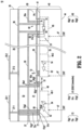
- FIG. 2 illustrates an exemplary configuration of a portion of antenna apparatus 10 in an assembled state, depicted in a cross-sectional view.
- wafer 40 electrically and mechanically connects to interposer 30 through a large number of solder balls (or copper pillars) 59 connected between lower metal layer 39 of interposer 30 and top surface 41 of wafer 40.
- solder balls 59 may number in the thousands.
- Interposer 30 further includes thin film metal layer 36 that may have been formed by electroplating on a top surface of upper layer 33.
- Radiating layer 20 may have been bonded to metal layer 36 by atomically growing multiple layers of an air / honeycomb dielectric material of dielectric 25 atop metal layer 36.
- a pre-cut slab of dielectric 25 is fused to metal layer 36 through direct bond interconnect (DBI) bonding, thermal compression bonding or other suitable process.
- DBI direct bond interconnect
- metal layer 36 may alternatively be formed first on the lower surface of dielectric 25 instead of the upper surface of interposer 30.
- FIG. 2 depicts two sub-circuits, 48-1 and 48-2 which are part of the same tile 42, and a sub-circuit 65 which may be part of the same tile or a different tile 42.
- Radiating layer 20 includes antenna elements 22-1, 22-2 connected to probe feeds 27-1, 27-2, each in turn connecting to a via 72s.
- This example illustrates via transition 72 embodied as a set of three vias that form part of a GSG connection: a "signal via" 72s, a first "ground via” 72g1, and a second ground via 72g2.
- Signal via 72s is connected on one end to probe feed 27-1 and on an opposite end to a "signal contact" 51s of sub-circuit 48-1 through a solder ball 59.
- Signal contact 51s in conjunction with a first ground contact 51g1 and a second ground contact 51g2 on opposite sides thereof, forms a set of GSG contacts 51.
- First and second ground vias 72g1, 72g2 connect on one end through a respective solder ball 59 to first and second ground contacts 51g1, 51g2, respectively, and on an opposite end to ground plane 36.
- a via transition 82 may serve as a stripline to CPW, stripline to microstrip or stripline to stripline transition, depending on the type of transmission line interface within wafer 40.
- each via transition 82 may include a signal via 82s (a blind via) connected between the central conductor within layer 37 and a signal contact 51s; a ground via 82g1 connected between ground plane 36 and a ground contact 51g1; and an adjacent connection (through a solder ball 59) between ground contact 51g2 and lower ground plane 39.
- signal vias 72s are examples of “first vias”
- signal vias 82s are examples of "second vias”.
- Each sub-circuit 48 includes one or more beamforming components such as an amplifier 52 and a phase shifter 54.
- Sub-circuits 48 of different tiles 42 are effectively interconnected by vias 82s connecting to combiner / divider 35.
- Any sub-circuit 48 may receive control signals or bias signals CNT on a control line(s) 47, to control one or more active components therein.
- Control lines 47 may connect to an external component through an input terminal on a bottom surface 44 of wafer 40.
- the beamforming components of a sub-circuit 48 may modify (e.g., amplify, phase shift, and/or filter) a transmit signal received from combiner/divider 35 through on-wafer combiner/divider 49, and output the modified transmit signal to a respective antenna element 22.
- a reciprocal operation may occur in the receive path direction with the use of T/R switches (not shown) and/or circuitry to implement a full-duplex or other transmit-receive isolation scheme.
- T/R switches not shown
- circuitry to implement a full-duplex or other transmit-receive isolation scheme.
- combiner/divider 49 is implemented as CPW
- the conductors of the CPW or the microstrip conductor may have been formed on surface 41 of wafer 40 as illustrated. Since solder balls 59 have a diameter large enough to create a gap 77 between the opposing surfaces of wafer 40 and interposer 30, the gap 77 may be sufficient to prevent ground plane 39 from shorting or adversely affecting the signals carried by the CPW or microstrip conductors.
- a sub-circuit 48 may further include a divider (not shown) that divides the modified transmit signal (e.g., output by amplifier 52) to feed two or more antenna elements 22. Such a divider may perform a reciprocal combining operation in the receive direction.
- combiner/divider 35 has an input signal path 35a that is broken at the metal layer 37 level and routed down through a via transition 82 to a transmit amplifier 62 of a sub-circuit 65.
- the amplified transmit signal output by amplifier 62 is then routed back to combiner/divider 35 through another via transition 82.
- amplifier 62 may restore the magnitude of the transmit signal to a desirable level.
- a receive path amplifier (not shown) may be similarly deployed within sub-circuit 65. In this case, T/R switches or other isolation circuitry may be included within sub-circuit 65 to isolate the transmit and receive signals.
- I/O point p4 may receive the input transmit signal and/or output the receive signal through a connector (not shown) attached at a side surface of interposer 30.
- an I/O connector (not shown) is attached at the bottom surface 44 of wafer 40.
- I/O point p4 may connect to the I/O connector through another via transition 82.
- the latter via transition 82 would connect to wafer 40 at a connection point corresponding to a top end of a via in wafer 40, or a coaxial feed-through in wafer 40.
- the bottom end of the via or feed-through in wafer 40 would connect to the I/O connector at the bottom surface 44.
- sub-circuits 48 of the same or different tiles may be connected to each other for RF signal and/or control signal routing through interconnect paths of interposer 30.
- An interconnect path between sub-circuits 48 may be formed at the metal layer 37 by using blind vias such as 82s, and/or another metal layer at a different level (not shown) within interposer 30.
- sub-circuits 48-1 and 48-2 of FIG. 2 are alternatively sub-circuits of different tiles 42, a saw street region 55 exists between the tiles 42. Since no metallization is applied to the top surface 41 of wafer 40 in saw street region 55, "inter-tile" connections between sub-circuits 48 may be made through interposer 30 in this manner through layer 37.
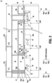
- FIG. 3 illustrates another exemplary configuration of antenna apparatus 10 in an assembled state.
- This configuration differs from that of FIG. 2 by omitting solder balls 59 and instead forming a direct bond between interposer 30 and wafer 40, e.g., through a DBI bonding method.
- this approach eliminates thousands of solder balls 59, thereby improving reliability of antenna apparatus 10.
- an isolation layer may have been deposited atop any conductor on or near wafer surface 41.
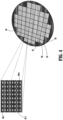
- FIG. 4 illustrates an exemplary tile arrangement on a wafer and an exemplary tile configuration of antenna apparatus 10.
- a tile denotes circuitry formed within a wafer with the use of a reticle-based image applied to a specific physical surface, herein referred to as a "tile region".
- a disc-shaped wafer 40 may have tiles 42 formed in rows and columns, with saw streets 55 between adjacent tiles 42. The tiles 42, however, are not cut from wafer along the saw streets 55, contrary to conventional designs.
- a tile such as 42-1 may include a grid layout of sub-circuits 48-1 to 48-w (of which one or more may be a sub-circuit 65 discussed earlier). In some examples, only complete rectangular or square tiles 42 are formed as part of wafer 40, leaving some peripheral surface area of wafer 40 unused. In other examples, additional sub-circuits may be formed at the circular perimeter of the wafer.
- FIG. 5 schematically illustrates how tiles of wafer 40 may be formed using a reticle.
- a reticle 90 is a tool that produces a photolithographic image 91 that patterns a film or mask (already deposited on the wafer) to expose regions for processing and ultimately form a complete circuit after many process steps.
- Image 91 has a span "d" that is typically limited in extent to only a portion of a wafer 40's diameter. Typically, the span d is less than half the wafer 40's diameter in order to generate a circuit image at the wafer 40 surface with a target resolution.
- An identical image is generated in tile regions across wafer 40. The identical image may be generated by stepping reticle 90 laterally and repeating the illumination with the same image 91.
- FIG. 1 schematically illustrates how tiles of wafer 40 may be formed using a reticle.
- reticle 90 initially produces a first image 91 to generate a first exposure for tile 42-i.
- Reticle 90 is then laterally translated as illustrated by path 93 and produces a second image 91 which is the same as the first image, to produce a first exposure for second tile 42-(i+1).
- the process may be repeated for all tile regions of wafer 40.
- a first processing step such as ion implantation for doping transistor regions, or electroplating to deposit a first metallization layer, may be performed simultaneously on wafer 40 for all tile regions.
- reticle 90 may be again controlled to begin a second round of tile region to tile region exposures corresponding to a second processing step, and so on, until all processing steps are completed.
- saw streets 55 between the adjacent tiles are formed, which are isolation regions without metal, traditionally used to dice tiles or individual chips from the wafer.
- no dicing between tiles 42 is performed, thereby producing wafer 40 as a continuous substrate with many tiles 42 formed therein.
- FIG. 6 depicts an exemplary layout of consecutive tiles on a wafer 40 of antenna apparatus 10 according to an example.
- Tiles 42-i, 42-(i+1) and 42-(i+2) are arranged in a given row of wafer 40, with saw streets 55 between adjacent tiles.
- Each tile 42 may have a plurality of interconnected sub-circuits 48-1 to 48-w, which, to form conventional devices, would be diced from the wafer along regions 66 (and also along saw streets 55) to form individual chips that would be re-attached to a substrate.
- no chips are diced and each tile such as 42-i may have a plurality of on-wafer combiner/dividers such as 49-1 and 49-2.
- FIG. 7A schematically illustrates an exemplary connection and signal flow among sub-circuits 48 within the same tile such as 42-i of FIG. 6 , interconnected using interposer 30.
- FIG. 7B is a functional block diagram for this example.
- an RF signal output from sub-circuit 48-j is divided between paths 35c and 35d of combiner/divider 35 within interposer 30.
- the divided signals are re-routed back to wafer 40 through respective paths 722, 724 (e.g., via transitions 82), which connect to on-wafer dividers 49-1, 49-2 at points p6 and p7, respectively.
- On-wafer dividers 49-1, 49-2 each divide the signals again among multiple paths, and these divided signals are provided to adjacent sub-circuit pairs (48-(j-2), 48-(j-1)) and (48-(j+1), 48-(j+2), respectively.
- Each sub-circuit 48 may modify the input signal and output the modified signal through interposer 30 to an antenna element 22 as depicted by paths 713. Reciprocal signal flow may occur in the receive direction.
- FIG. 8 schematically illustrates an exemplary connection configuration between sub-circuits of different tiles and signal routing across tiles in antenna apparatus 10 according to an embodiment.
- an RF signal originating from a sub-circuit 48-P of a tile 42-(i+1) is output through interposer 30 and split among paths 35f and 35g of combiner/divider 35.
- Path 35f traverses over saw street 55 and connects through a via transition 82 to an on-wafer divider 49-u of an adjacent tile 42-i.
- Path 35g traverses over tile 42-(i+1) and connects through another via transition 82 to an on-wafer divider 49-v.
- the on-wafer dividers 49-u, 49-v split the signals again between adjacent sub-circuits 48 for modification and outputting to antenna array 23. Reciprocal signal flow may occur in the receive direction.
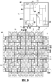
- FIG. 9 illustrates an exemplary tile layout along with a signal routing example according to an embodiment of antenna apparatus 10.
- a wafer 40 includes a grid layout of sixty tiles 42-1 to 42-60, with one tile omitted from each corner of a square profile.
- Each sub-circuit 48 may include a set of contacts 51 as described above to connect to a respective antenna element 22 through a via transition 72.
- FIGS. 9 represent paths of an exemplary combiner / divider 35 within interposer 30.
- An RF I/O connection point p4 located within interposer 30 near a centralized edge of wafer 40 connects to an input path 35a.
- Input path 35a extends to a centralized point p8 of interposer 30, where it divides to feed left side and right side tiles 42.
- a transmit signal is re-routed by a via transition 82 from combiner/divider 35 to an amplifier 65-1 of a tile 42 on each side. There, it is amplified and routed back to combiner/divider 35 by another via transition 82 for further division at a point p9 towards tiles in upper and lower quadrants. Downstream, further division by combiner/divider 35 and amplification by amplifiers such as 65-2 may occur as necessary or desired to restore the divided transmit signals to a suitable level.
- a transmit signal destined for tile 42-j may be routed from interposer 30 to an intermediate amplifier 65 through a via transition 82 and amplified.
- the amplified output may be routed back up to combiner/divider 35 where it may divide into two paths, one of which may terminate at an end point 35ej.
- another via transition 82 may route the signal back to on-wafer combiner/divider 49-j.
- combiner/divider 49-j is a 1:16 power divider/combiner with 16 termination points connected to respective sub-circuits 48-1 to 48-16 for transmission through antenna elements 22. Reciprocal operations may occur in the receive paths from antenna elements 22.
- amplifiers 65 may be provided in each tile 42, some amplifiers 65 may be actively used whereas others are unused (unconnected and/or turned off).
- a selection of which amplifiers 65 to use, and how to bias them for variable amplification, may depend on the overall layout of the tiles 42 and a target electric field (antenna current) distribution across the aperture of antenna array 23. For example, instead of designing for a uniform electric field distribution, outer antenna elements may be fed with less RF power to achieve a target antenna pattern with lower sidelobes.
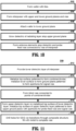
- FIG. 10 is a flow diagram of an exemplary method of forming antenna apparatus 10 having an interposer with stripline construction.
- the order of the various process steps of the method may be changed as desired.
- a wafer 40 is formed with multiple tiles (S102) using a reticle as described above with respect to FIG. 5 .
- An interposer 30 with a stripline construction is formed (S104), where the interposer includes upper and lower ground planes and vias (e.g. blind vias 82s and "complete vias" 82g1, 72s, 72g1, 72g2 extending completely between lower and upper surfaces of the interposer).
- the wafer is attached to the interposer's lower ground plane (S106) using either the solder ball connection scheme ( FIG. 2 ) or the direct attachment method ( FIG. 3 ) described earlier.
- a dielectric layer of radiating layer 20 may be grown (S108) atop the upper ground plane.
- the material of the dielectric layer may be an air / honeycomb material grown atomically layer by layer.
- antenna elements may be formed atop the dielectric layer and probe feed vias may be formed through the dielectric layer (S110), thereby completing the antenna apparatus 10 fabrication.
- the probe feed vias connect on one end to the antenna element metallization and on the opposite end to the top metallization of the interposer signal vias 72s.
- FIG. 11 is a flow diagram of exemplary process steps for forming the interposer of the method of FIG. 10 , representing an example for process S104.
- the order of the various process steps of this method may be changed as desired.
- a lower dielectric layer of the interposer is provided (S112).
- the top surface of the lower dielectric layer is metallized (S114) in a pattern to form combiner/divider 35; and the bottom surface of the lower dielectric layer is metallized with a pattern to form the lower ground plane 39 with apertures for signal vias 72s and 82s.
- the apertures prevent the signal vias from shorting to the lower ground plane.
- a metallized pattern may be formed with a centralized metal disc or square for a via pad, surrounded by an isolation ring with metal removed, which is in turn surrounded by ground plane metal.
- Blind vias 82s of via transitions 82, connected to points of the combiner/divider 35, may be formed (S116).
- the upper dielectric layer of the stripline may then be formed or attached on the metallized top surface of the lower substrate (S118).
- the top surface of the dielectric layer may be metallized in a pattern to form the upper ground plane with similar apertures to allow an isolated connection between the probe feed vias and the signal vias 72s. Holes may then be drilled for the via transitions 72 and the complete vias 82g1 of via transitions 82; and the holes are filled with metal to complete the formation of the vias (S120), thereby completing the interposer 30 fabrication.
- Embodiments of antenna apparatus as described above may be formed with a low profile and achieve superior performance (e.g., lower loss and higher frequency operation) as compared to conventional designs. Further, the construction is amenable to a facilitated manufacturing process.
- an interposer with vias to interconnect reticle-image-based tiles across saw street isolation regions, a large number of beamforming circuits can be internally formed within a single wafer.
- An array-sized wafer with beamforming circuits may thereby be fabricated without the need to dice and re-attach individual chips to a substrate. Furthermore, regions within the wafer otherwise allocated for a combiner/divider network can be freed up for other purposes.
Landscapes
- Engineering & Computer Science (AREA)
- Microelectronics & Electronic Packaging (AREA)
- Manufacturing & Machinery (AREA)
- Variable-Direction Aerials And Aerial Arrays (AREA)
- Semiconductor Integrated Circuits (AREA)
Claims (15)
- Appareil d'antenne (10) comprenant :une couche rayonnante (20) comprenant une pluralité d'éléments d'antenne (22) formant un réseau antennaire ;une tranche de semi-conducteur (40) comprenant une pluralité de tuiles (42) possédant chacune des circuits de formation de faisceaux (48) ; etun interposeur multicouche (30) comprenant :une couche diélectrique inférieure (31) adjacente à la tranche ;une couche diélectrique supérieure (33) adjacente à la couche rayonnante ;une couche métallique (37) entre les couches diélectriques inférieure et supérieure et comprenant une pluralité de traces conductrices (35) ;une pluralité de premiers vias (72) s'étendant à travers à la fois les couches diélectriques supérieure et inférieure et couplant électriquement les circuits de formation de faisceaux à la pluralité d'éléments d'antenne ; etune pluralité de seconds vias (82) s'étendant entre les circuits de formation de faisceau et les traces conductrices pour interconnecter la pluralité de tuiles, chacune de la pluralité de tuiles possédant une configuration de circuit identique formée par une image générée par réticule identique (91).
- Appareil d'antenne (10) de la revendication 1, ladite tranche comprenant en outre des chemins de scie (55) séparant la pluralité de tuiles les unes des autres.
- Appareil d'antenne (10) de la revendication 1, lesdits premiers vias étant chacun un via de signal (72s) d'une transition de via masse-signal-masse, GSG,
qui comprend en outre un premier via de masse (72g1) sur un côté du via de signal et un second via de masse (72g2) sur un autre côté du via de signal. - Appareil d'antenne (10) de la revendication 3,ledit interposeur multicouche (30) possédant une construction à ligne ruban comprenant la première couche diélectrique, la seconde couche diélectrique, un plan de masse inférieur (39) entre la tranche et la couche diélectrique inférieure, et un plan de masse supérieur (36) entre la couche diélectrique supérieure et la couche rayonnante, le plan de masse supérieur servant de plan de masse aux éléments d'antenne ;lesdits premier et second vias de masse sont respectivement connectés sur une extrémité aux premier et deuxième contacts de masse respectifs (51g1, 51g2) sur la tranche et sont chacun connectés sur une extrémité opposée au plan de masse supérieur.
- Appareil d'antenne (10) de la revendication 4, lesdits seconds vias (82s) étant chacun un via de signal d'une transition de via qui comprend en outre un via de masse (82g1) connectant un troisième contact de masse de la tranche au plan de masse supérieur et une connexion masse-masse connectant un quatrième contact de masse de la tranche au plan de masse inférieur.
- Appareil d'antenne (10) de la revendication 1, lesdites traces conductrices de la couche métallique faisant partie d'un réseau combineur/diviseur (35) qui diviseun signal d'émission radiofréquence, RF, reçu au niveau d'un point de connexion d'entrée/sortie, E/S (P4) del'interposeur en une pluralité de signaux d'émission RF divisés, chacun acheminé vers un ou plusieurs des circuits de formation de faisceaux à l'aide de l'un respectif des seconds vias au niveau d'un point d'extrémité respectif (35e) du réseau combineur/diviseur.
- Appareil d'antenne (10) de la revendication 6, ledit signal d'émission RF étant reçu au niveau du point de connexion E/S en provenance d'un point de connexion sur la tranche, à l'aide d'un via supplémentaire (82) à l'intérieur de l'interposeur.
- Appareil d'antenne (10) de la revendication 6,chacun des signaux d'émission divisés étant acheminé vers une tuile respective de la pluralité de tuiles au niveau du point d'extrémité respectif du réseau combineur/diviseur ; etladite tuile respective comprenant en outre un combineur/diviseur sur tranche, connecté électriquement au point d'extrémité respectif, qui divise en outre le signal divisé en au moins deux autres signaux divisés et achemine chaque signal divisé en outre vers l'un respectif des circuits de formation de faisceaux de la tuile respective.
- Appareil d'antenne (10) de la revendication 1, ladite pluralité de traces conductrices formant un réseau combineur/diviseur (35), et au moins l'une de la pluralité de tuiles comprenant un amplificateur intermédiaire qui amplifie un signal d'émission ou un signal de réception acheminé par le réseau combineur/diviseur, par un autre via à l'intérieur de l'interposeur, en provenance/vers un point intermédiaire du réseau combineur/diviseur et renvoie le signal d'émission ou de réception amplifié vers le réseau combineur/diviseur par un via supplémentaire (82).
- Appareil d'antenne (10) de la revendication 1, ladite pluralité de traces conductrices formant un réseau combineur/diviseur (35), et chacune de la pluralité de tuiles comprenant un amplificateur intermédiaire (65) pouvant être connecté sur un côté entrée par un autre via (82) à l'intérieur de l'interposeur à un point intermédiaire respectif du combineur/diviseur et un côté sortie pouvant être connecté par un autre via à un autre point intermédiaire respectif du combineur/diviseur, chaque amplificateur intermédiaire étant configuré pour amplifier sélectivement un signal d'émission ou un signal de réception acheminé par le réseau combineur/diviseur.
- Appareil d'antenne (10) de la revendication 1, ladite pluralité de traces conductrices formant un réseau combineur/diviseur (35) qui combine une pluralité de signaux de réception radiofréquence (RF) reçus par les éléments d'antenne et réglés par les circuits de formation de faisceaux en un signal de réception RF combiné délivré en sortie à l'aide d'un via supplémentaire à l'intérieur de l'interposeur à un point de connexion sur la tranche.
- Appareil d'antenne (10) de la revendication 1, comprenant en outre une pluralité de bosses de soudure (59) connectant chacune électriquement l'un respectif des premiers vias ou des seconds vias à la tranche.
- Appareil d'antenne (10) de la revendication 1, ladite tranche étant directement liée à l'interposeur multicouche.
- Appareil d'antenne (10) de la revendication 1, ladite couche rayonnante comprenant un matériau air-diélectrique développé sur l'interposeur et supportant les éléments d'antenne.
- Appareil d'antenne de la revendication 1, lesdits éléments d'antenne étant des éléments d'antenne planaire pilotés chacun par une alimentation de sonde (27) couplée électriquement à l'un des premiers vias.
Applications Claiming Priority (2)
| Application Number | Priority Date | Filing Date | Title |
|---|---|---|---|
| US16/655,523 US11049824B2 (en) | 2019-10-17 | 2019-10-17 | Antenna apparatus with integrated antenna array and low loss multi-layer interposer |
| PCT/US2020/055294 WO2021076459A1 (fr) | 2019-10-17 | 2020-10-12 | Appareil d'antenne à réseau antennaire intégré et interposeur multicouche à faible perte |
Publications (3)
| Publication Number | Publication Date |
|---|---|
| EP4000129A1 EP4000129A1 (fr) | 2022-05-25 |
| EP4000129B1 true EP4000129B1 (fr) | 2023-07-19 |
| EP4000129C0 EP4000129C0 (fr) | 2023-07-19 |
Family
ID=74106104
Family Applications (1)
| Application Number | Title | Priority Date | Filing Date |
|---|---|---|---|
| EP20833991.1A Active EP4000129B1 (fr) | 2019-10-17 | 2020-10-12 | Appareil d'antenne à réseau antennaire intégré et interposeur multicouche à faible perte |
Country Status (9)
| Country | Link |
|---|---|
| US (1) | US11049824B2 (fr) |
| EP (1) | EP4000129B1 (fr) |
| JP (1) | JP7714531B2 (fr) |
| KR (1) | KR102802028B1 (fr) |
| CN (1) | CN114424402B (fr) |
| AU (1) | AU2020366303B2 (fr) |
| BR (1) | BR112022004755A2 (fr) |
| IL (1) | IL291376B2 (fr) |
| WO (1) | WO2021076459A1 (fr) |
Families Citing this family (11)
| Publication number | Priority date | Publication date | Assignee | Title |
|---|---|---|---|---|
| US9825597B2 (en) | 2015-12-30 | 2017-11-21 | Skyworks Solutions, Inc. | Impedance transformation circuit for amplifier |
| US10297913B2 (en) * | 2016-05-04 | 2019-05-21 | Skyworks Solutions, Inc. | Shielded radio frequency component with integrated antenna |
| TWI907080B (zh) | 2016-12-29 | 2025-12-01 | 美商天工方案公司 | 封裝模組、無線通信裝置及射頻信號傳輸方法 |
| US10515924B2 (en) | 2017-03-10 | 2019-12-24 | Skyworks Solutions, Inc. | Radio frequency modules |
| US12003031B2 (en) * | 2019-11-21 | 2024-06-04 | The Board Of Regents Of The University Of Oklahoma | Dual-polarized microstrip patch antenna and array |
| CN111146579A (zh) * | 2020-01-17 | 2020-05-12 | 惠州Tcl移动通信有限公司 | 天线装置及终端设备 |
| WO2021179160A1 (fr) | 2020-03-10 | 2021-09-16 | 京东方科技集团股份有限公司 | Antenne et son procédé de fabrication, et système d'antenne |
| US11450954B2 (en) | 2020-04-01 | 2022-09-20 | Elwha, Llc | Beamforming via sparse activation of antenna elements connected to phase advance waveguides |
| US12407087B2 (en) * | 2021-04-09 | 2025-09-02 | Taiwan Semiconductor Manufacturing Company, Ltd. | Semiconductor structures and method of forming the same |
| US20230140738A1 (en) * | 2021-10-30 | 2023-05-04 | Raymond Won Bae | Microelectronic test and package interface substrates, devices, and methods of manufacture thereof alignment improvement of interconnect on buildup redistribution layers |
| CN119517903B (zh) * | 2024-11-20 | 2025-11-18 | 中国电子科技集团公司第五十五研究所 | 一种刚柔混合三维晶圆架构毫米波晶上阵列 |
Family Cites Families (12)
| Publication number | Priority date | Publication date | Assignee | Title |
|---|---|---|---|---|
| JPH11274029A (ja) * | 1998-03-19 | 1999-10-08 | Asahi Kasei Micro Syst Co Ltd | スキャニングステッパー |
| US6421012B1 (en) * | 2000-07-19 | 2002-07-16 | Harris Corporation | Phased array antenna having patch antenna elements with enhanced parasitic antenna element performance at millimeter wavelength radio frequency signals |
| US7423607B2 (en) | 2006-09-28 | 2008-09-09 | Farrokh Mohamadi | Switching power amplifier and DAC for an electronically-scanned array |
| US8232920B2 (en) * | 2008-08-07 | 2012-07-31 | International Business Machines Corporation | Integrated millimeter wave antenna and transceiver on a substrate |
| FR2969397B1 (fr) | 2010-12-20 | 2013-09-06 | St Microelectronics Crolles 2 | Emetteur-recepteur integre en ondes millimetriques |
| US8648454B2 (en) * | 2012-02-14 | 2014-02-11 | International Business Machines Corporation | Wafer-scale package structures with integrated antennas |
| US9472859B2 (en) | 2014-05-20 | 2016-10-18 | International Business Machines Corporation | Integration of area efficient antennas for phased array or wafer scale array antenna applications |
| US10541461B2 (en) * | 2016-12-16 | 2020-01-21 | Ratheon Company | Tile for an active electronically scanned array (AESA) |
| US20180197829A1 (en) * | 2017-01-09 | 2018-07-12 | Qorvo Us, Inc. | Three-dimensional integrated circuit assembly with active interposer |
| US10367256B2 (en) * | 2017-06-26 | 2019-07-30 | Avl Technologies, Inc. | Active electronically steered array for satellite communications |
| US10784563B2 (en) | 2018-02-21 | 2020-09-22 | International Business Machines Corporation | Scalable phased array package |
| US10916854B2 (en) * | 2018-03-29 | 2021-02-09 | Mediatek Inc. | Antenna structure with integrated coupling element and semiconductor package using the same |
-
2019
- 2019-10-17 US US16/655,523 patent/US11049824B2/en active Active
-
2020
- 2020-10-12 KR KR1020227016014A patent/KR102802028B1/ko active Active
- 2020-10-12 WO PCT/US2020/055294 patent/WO2021076459A1/fr not_active Ceased
- 2020-10-12 EP EP20833991.1A patent/EP4000129B1/fr active Active
- 2020-10-12 IL IL291376A patent/IL291376B2/en unknown
- 2020-10-12 BR BR112022004755A patent/BR112022004755A2/pt unknown
- 2020-10-12 AU AU2020366303A patent/AU2020366303B2/en active Active
- 2020-10-12 CN CN202080065514.9A patent/CN114424402B/zh active Active
- 2020-10-12 JP JP2022518630A patent/JP7714531B2/ja active Active
Also Published As
| Publication number | Publication date |
|---|---|
| JP2023502559A (ja) | 2023-01-25 |
| IL291376B2 (en) | 2024-09-01 |
| JP7714531B2 (ja) | 2025-07-29 |
| US11049824B2 (en) | 2021-06-29 |
| US20210118828A1 (en) | 2021-04-22 |
| CN114424402B (zh) | 2025-08-15 |
| WO2021076459A1 (fr) | 2021-04-22 |
| EP4000129A1 (fr) | 2022-05-25 |
| CN114424402A (zh) | 2022-04-29 |
| BR112022004755A2 (pt) | 2022-06-21 |
| IL291376B1 (en) | 2024-05-01 |
| AU2020366303A1 (en) | 2022-03-03 |
| KR20220071979A (ko) | 2022-05-31 |
| IL291376A (en) | 2022-05-01 |
| KR102802028B1 (ko) | 2025-04-30 |
| EP4000129C0 (fr) | 2023-07-19 |
| AU2020366303B2 (en) | 2026-03-26 |
Similar Documents
| Publication | Publication Date | Title |
|---|---|---|
| EP4000129B1 (fr) | Appareil d'antenne à réseau antennaire intégré et interposeur multicouche à faible perte | |
| US11757203B2 (en) | Low profile antenna apparatus | |
| US20260051648A1 (en) | Antenna array architecture with electrically conductive columns between substrates | |
| KR102873900B1 (ko) | 다수의 표면 인터페이스를 갖는 빔포머 ic 칩을 갖는 집적 안테나 어레이 | |
| US12444858B2 (en) | Antenna apparatus employing coplanar waveguide interconnect between RF components | |
| WO2024206457A1 (fr) | Antennes réseau à commande de phase utilisant un système d'élément d'antenne dans un boîtier |
Legal Events
| Date | Code | Title | Description |
|---|---|---|---|
| STAA | Information on the status of an ep patent application or granted ep patent |
Free format text: STATUS: UNKNOWN |
|
| STAA | Information on the status of an ep patent application or granted ep patent |
Free format text: STATUS: THE INTERNATIONAL PUBLICATION HAS BEEN MADE |
|
| PUAI | Public reference made under article 153(3) epc to a published international application that has entered the european phase |
Free format text: ORIGINAL CODE: 0009012 |
|
| STAA | Information on the status of an ep patent application or granted ep patent |
Free format text: STATUS: REQUEST FOR EXAMINATION WAS MADE |
|
| 17P | Request for examination filed |
Effective date: 20220218 |
|
| AK | Designated contracting states |
Kind code of ref document: A1 Designated state(s): AL AT BE BG CH CY CZ DE DK EE ES FI FR GB GR HR HU IE IS IT LI LT LU LV MC MK MT NL NO PL PT RO RS SE SI SK SM TR |
|
| DAV | Request for validation of the european patent (deleted) | ||
| DAX | Request for extension of the european patent (deleted) | ||
| GRAP | Despatch of communication of intention to grant a patent |
Free format text: ORIGINAL CODE: EPIDOSNIGR1 |
|
| STAA | Information on the status of an ep patent application or granted ep patent |
Free format text: STATUS: GRANT OF PATENT IS INTENDED |
|
| INTG | Intention to grant announced |
Effective date: 20230210 |
|
| GRAS | Grant fee paid |
Free format text: ORIGINAL CODE: EPIDOSNIGR3 |
|
| GRAA | (expected) grant |
Free format text: ORIGINAL CODE: 0009210 |
|
| STAA | Information on the status of an ep patent application or granted ep patent |
Free format text: STATUS: THE PATENT HAS BEEN GRANTED |
|
| P01 | Opt-out of the competence of the unified patent court (upc) registered |
Effective date: 20230525 |
|
| AK | Designated contracting states |
Kind code of ref document: B1 Designated state(s): AL AT BE BG CH CY CZ DE DK EE ES FI FR GB GR HR HU IE IS IT LI LT LU LV MC MK MT NL NO PL PT RO RS SE SI SK SM TR |
|
| REG | Reference to a national code |
Ref country code: GB Ref legal event code: FG4D |
|
| REG | Reference to a national code |
Ref country code: CH Ref legal event code: EP |
|
| REG | Reference to a national code |
Ref country code: DE Ref legal event code: R096 Ref document number: 602020014214 Country of ref document: DE |
|
| REG | Reference to a national code |
Ref country code: IE Ref legal event code: FG4D |
|
| U01 | Request for unitary effect filed |
Effective date: 20230816 |
|
| U07 | Unitary effect registered |
Designated state(s): AT BE BG DE DK EE FI FR IT LT LU LV MT NL PT SE SI Effective date: 20230821 |
|
| P04 | Withdrawal of opt-out of the competence of the unified patent court (upc) registered |
Effective date: 20230817 |
|
| REG | Reference to a national code |
Ref country code: LT Ref legal event code: MG9D |
|
| U20 | Renewal fee for the european patent with unitary effect paid |
Year of fee payment: 4 Effective date: 20231027 |
|
| PG25 | Lapsed in a contracting state [announced via postgrant information from national office to epo] |
Ref country code: GR Free format text: LAPSE BECAUSE OF FAILURE TO SUBMIT A TRANSLATION OF THE DESCRIPTION OR TO PAY THE FEE WITHIN THE PRESCRIBED TIME-LIMIT Effective date: 20231020 |
|
| PG25 | Lapsed in a contracting state [announced via postgrant information from national office to epo] |
Ref country code: IS Free format text: LAPSE BECAUSE OF FAILURE TO SUBMIT A TRANSLATION OF THE DESCRIPTION OR TO PAY THE FEE WITHIN THE PRESCRIBED TIME-LIMIT Effective date: 20231119 |
|
| PG25 | Lapsed in a contracting state [announced via postgrant information from national office to epo] |
Ref country code: RS Free format text: LAPSE BECAUSE OF FAILURE TO SUBMIT A TRANSLATION OF THE DESCRIPTION OR TO PAY THE FEE WITHIN THE PRESCRIBED TIME-LIMIT Effective date: 20230719 Ref country code: NO Free format text: LAPSE BECAUSE OF FAILURE TO SUBMIT A TRANSLATION OF THE DESCRIPTION OR TO PAY THE FEE WITHIN THE PRESCRIBED TIME-LIMIT Effective date: 20231019 Ref country code: IS Free format text: LAPSE BECAUSE OF FAILURE TO SUBMIT A TRANSLATION OF THE DESCRIPTION OR TO PAY THE FEE WITHIN THE PRESCRIBED TIME-LIMIT Effective date: 20231119 Ref country code: HR Free format text: LAPSE BECAUSE OF FAILURE TO SUBMIT A TRANSLATION OF THE DESCRIPTION OR TO PAY THE FEE WITHIN THE PRESCRIBED TIME-LIMIT Effective date: 20230719 Ref country code: GR Free format text: LAPSE BECAUSE OF FAILURE TO SUBMIT A TRANSLATION OF THE DESCRIPTION OR TO PAY THE FEE WITHIN THE PRESCRIBED TIME-LIMIT Effective date: 20231020 |
|
| PG25 | Lapsed in a contracting state [announced via postgrant information from national office to epo] |
Ref country code: PL Free format text: LAPSE BECAUSE OF FAILURE TO SUBMIT A TRANSLATION OF THE DESCRIPTION OR TO PAY THE FEE WITHIN THE PRESCRIBED TIME-LIMIT Effective date: 20230719 |
|
| REG | Reference to a national code |
Ref country code: DE Ref legal event code: R097 Ref document number: 602020014214 Country of ref document: DE |
|
| PG25 | Lapsed in a contracting state [announced via postgrant information from national office to epo] |
Ref country code: ES Free format text: LAPSE BECAUSE OF FAILURE TO SUBMIT A TRANSLATION OF THE DESCRIPTION OR TO PAY THE FEE WITHIN THE PRESCRIBED TIME-LIMIT Effective date: 20230719 |
|
| PG25 | Lapsed in a contracting state [announced via postgrant information from national office to epo] |
Ref country code: SM Free format text: LAPSE BECAUSE OF FAILURE TO SUBMIT A TRANSLATION OF THE DESCRIPTION OR TO PAY THE FEE WITHIN THE PRESCRIBED TIME-LIMIT Effective date: 20230719 Ref country code: RO Free format text: LAPSE BECAUSE OF FAILURE TO SUBMIT A TRANSLATION OF THE DESCRIPTION OR TO PAY THE FEE WITHIN THE PRESCRIBED TIME-LIMIT Effective date: 20230719 Ref country code: ES Free format text: LAPSE BECAUSE OF FAILURE TO SUBMIT A TRANSLATION OF THE DESCRIPTION OR TO PAY THE FEE WITHIN THE PRESCRIBED TIME-LIMIT Effective date: 20230719 Ref country code: CZ Free format text: LAPSE BECAUSE OF FAILURE TO SUBMIT A TRANSLATION OF THE DESCRIPTION OR TO PAY THE FEE WITHIN THE PRESCRIBED TIME-LIMIT Effective date: 20230719 Ref country code: SK Free format text: LAPSE BECAUSE OF FAILURE TO SUBMIT A TRANSLATION OF THE DESCRIPTION OR TO PAY THE FEE WITHIN THE PRESCRIBED TIME-LIMIT Effective date: 20230719 |
|
| PLBE | No opposition filed within time limit |
Free format text: ORIGINAL CODE: 0009261 |
|
| STAA | Information on the status of an ep patent application or granted ep patent |
Free format text: STATUS: NO OPPOSITION FILED WITHIN TIME LIMIT |
|
| PG25 | Lapsed in a contracting state [announced via postgrant information from national office to epo] |
Ref country code: MC Free format text: LAPSE BECAUSE OF FAILURE TO SUBMIT A TRANSLATION OF THE DESCRIPTION OR TO PAY THE FEE WITHIN THE PRESCRIBED TIME-LIMIT Effective date: 20230719 |
|
| REG | Reference to a national code |
Ref country code: CH Ref legal event code: PL |
|
| 26N | No opposition filed |
Effective date: 20240422 |
|
| PG25 | Lapsed in a contracting state [announced via postgrant information from national office to epo] |
Ref country code: CH Free format text: LAPSE BECAUSE OF NON-PAYMENT OF DUE FEES Effective date: 20231031 |
|
| PG25 | Lapsed in a contracting state [announced via postgrant information from national office to epo] |
Ref country code: CH Free format text: LAPSE BECAUSE OF NON-PAYMENT OF DUE FEES Effective date: 20231031 |
|
| PG25 | Lapsed in a contracting state [announced via postgrant information from national office to epo] |
Ref country code: IE Free format text: LAPSE BECAUSE OF NON-PAYMENT OF DUE FEES Effective date: 20231012 |
|
| PG25 | Lapsed in a contracting state [announced via postgrant information from national office to epo] |
Ref country code: IE Free format text: LAPSE BECAUSE OF NON-PAYMENT OF DUE FEES Effective date: 20231012 |
|
| U20 | Renewal fee for the european patent with unitary effect paid |
Year of fee payment: 5 Effective date: 20241028 |
|
| P05 | Withdrawal of opt-out of the competence of the unified patent court (upc) changed |
Free format text: CASE NUMBER: APP_562412/2023 Effective date: 20230821 |
|
| PG25 | Lapsed in a contracting state [announced via postgrant information from national office to epo] |
Ref country code: CY Free format text: LAPSE BECAUSE OF FAILURE TO SUBMIT A TRANSLATION OF THE DESCRIPTION OR TO PAY THE FEE WITHIN THE PRESCRIBED TIME-LIMIT; INVALID AB INITIO Effective date: 20201012 |
|
| PG25 | Lapsed in a contracting state [announced via postgrant information from national office to epo] |
Ref country code: HU Free format text: LAPSE BECAUSE OF FAILURE TO SUBMIT A TRANSLATION OF THE DESCRIPTION OR TO PAY THE FEE WITHIN THE PRESCRIBED TIME-LIMIT; INVALID AB INITIO Effective date: 20201012 |
|
| U20 | Renewal fee for the european patent with unitary effect paid |
Year of fee payment: 6 Effective date: 20251027 |
|
| PG25 | Lapsed in a contracting state [announced via postgrant information from national office to epo] |
Ref country code: TR Free format text: LAPSE BECAUSE OF FAILURE TO SUBMIT A TRANSLATION OF THE DESCRIPTION OR TO PAY THE FEE WITHIN THE PRESCRIBED TIME-LIMIT Effective date: 20230719 |
|
| PGFP | Annual fee paid to national office [announced via postgrant information from national office to epo] |
Ref country code: GB Payment date: 20251027 Year of fee payment: 6 |