EP4002440B1 - Modul zur entfernung eines falsch montierten lichtemittierenden elements und verfahren zur entfernung eines falsch montierten lichtemittierenden elements damit - Google Patents
Modul zur entfernung eines falsch montierten lichtemittierenden elements und verfahren zur entfernung eines falsch montierten lichtemittierenden elements damit Download PDFInfo
- Publication number
- EP4002440B1 EP4002440B1 EP19938073.4A EP19938073A EP4002440B1 EP 4002440 B1 EP4002440 B1 EP 4002440B1 EP 19938073 A EP19938073 A EP 19938073A EP 4002440 B1 EP4002440 B1 EP 4002440B1
- Authority
- EP
- European Patent Office
- Prior art keywords
- semiconductor light
- mis
- emitting elements
- assembled
- emitting element
- Prior art date
- Legal status (The legal status is an assumption and is not a legal conclusion. Google has not performed a legal analysis and makes no representation as to the accuracy of the status listed.)
- Active
Links
Images


Classifications
-
- H—ELECTRICITY
- H10—SEMICONDUCTOR DEVICES; ELECTRIC SOLID-STATE DEVICES NOT OTHERWISE PROVIDED FOR
- H10H—INORGANIC LIGHT-EMITTING SEMICONDUCTOR DEVICES HAVING POTENTIAL BARRIERS
- H10H20/00—Individual inorganic light-emitting semiconductor devices having potential barriers, e.g. light-emitting diodes [LED]
- H10H20/01—Manufacture or treatment
-
- H—ELECTRICITY
- H10—SEMICONDUCTOR DEVICES; ELECTRIC SOLID-STATE DEVICES NOT OTHERWISE PROVIDED FOR
- H10P—GENERIC PROCESSES OR APPARATUS FOR THE MANUFACTURE OR TREATMENT OF DEVICES COVERED BY CLASS H10
- H10P72/00—Handling or holding of wafers, substrates or devices during manufacture or treatment thereof
- H10P72/04—Apparatus for manufacture or treatment
- H10P72/0402—Apparatus for fluid treatment
-
- H—ELECTRICITY
- H10—SEMICONDUCTOR DEVICES; ELECTRIC SOLID-STATE DEVICES NOT OTHERWISE PROVIDED FOR
- H10P—GENERIC PROCESSES OR APPARATUS FOR THE MANUFACTURE OR TREATMENT OF DEVICES COVERED BY CLASS H10
- H10P72/00—Handling or holding of wafers, substrates or devices during manufacture or treatment thereof
- H10P72/70—Handling or holding of wafers, substrates or devices during manufacture or treatment thereof for supporting or gripping
- H10P72/74—Handling or holding of wafers, substrates or devices during manufacture or treatment thereof for supporting or gripping using temporarily an auxiliary support
-
- H—ELECTRICITY
- H10—SEMICONDUCTOR DEVICES; ELECTRIC SOLID-STATE DEVICES NOT OTHERWISE PROVIDED FOR
- H10P—GENERIC PROCESSES OR APPARATUS FOR THE MANUFACTURE OR TREATMENT OF DEVICES COVERED BY CLASS H10
- H10P74/00—Testing or measuring during manufacture or treatment of wafers, substrates or devices
- H10P74/23—Testing or measuring during manufacture or treatment of wafers, substrates or devices characterised by multiple measurements, corrections, marking or sorting processes
- H10P74/232—Testing or measuring during manufacture or treatment of wafers, substrates or devices characterised by multiple measurements, corrections, marking or sorting processes comprising connection or disconnection of parts of a device in response to a measurement
-
- H—ELECTRICITY
- H10—SEMICONDUCTOR DEVICES; ELECTRIC SOLID-STATE DEVICES NOT OTHERWISE PROVIDED FOR
- H10W—GENERIC PACKAGES, INTERCONNECTIONS, CONNECTORS OR OTHER CONSTRUCTIONAL DETAILS OF DEVICES COVERED BY CLASS H10
- H10W90/00—Package configurations
-
- H—ELECTRICITY
- H10—SEMICONDUCTOR DEVICES; ELECTRIC SOLID-STATE DEVICES NOT OTHERWISE PROVIDED FOR
- H10H—INORGANIC LIGHT-EMITTING SEMICONDUCTOR DEVICES HAVING POTENTIAL BARRIERS
- H10H20/00—Individual inorganic light-emitting semiconductor devices having potential barriers, e.g. light-emitting diodes [LED]
- H10H20/01—Manufacture or treatment
- H10H20/011—Manufacture or treatment of bodies, e.g. forming semiconductor layers
- H10H20/013—Manufacture or treatment of bodies, e.g. forming semiconductor layers having light-emitting regions comprising only Group III-V materials
- H10H20/0133—Manufacture or treatment of bodies, e.g. forming semiconductor layers having light-emitting regions comprising only Group III-V materials with a substrate not being Group III-V materials
- H10H20/01335—Manufacture or treatment of bodies, e.g. forming semiconductor layers having light-emitting regions comprising only Group III-V materials with a substrate not being Group III-V materials the light-emitting regions comprising nitride materials
-
- H—ELECTRICITY
- H10—SEMICONDUCTOR DEVICES; ELECTRIC SOLID-STATE DEVICES NOT OTHERWISE PROVIDED FOR
- H10H—INORGANIC LIGHT-EMITTING SEMICONDUCTOR DEVICES HAVING POTENTIAL BARRIERS
- H10H20/00—Individual inorganic light-emitting semiconductor devices having potential barriers, e.g. light-emitting diodes [LED]
- H10H20/01—Manufacture or treatment
- H10H20/011—Manufacture or treatment of bodies, e.g. forming semiconductor layers
- H10H20/013—Manufacture or treatment of bodies, e.g. forming semiconductor layers having light-emitting regions comprising only Group III-V materials
- H10H20/0137—Manufacture or treatment of bodies, e.g. forming semiconductor layers having light-emitting regions comprising only Group III-V materials the light-emitting regions comprising nitride materials
-
- H—ELECTRICITY
- H10—SEMICONDUCTOR DEVICES; ELECTRIC SOLID-STATE DEVICES NOT OTHERWISE PROVIDED FOR
- H10H—INORGANIC LIGHT-EMITTING SEMICONDUCTOR DEVICES HAVING POTENTIAL BARRIERS
- H10H20/00—Individual inorganic light-emitting semiconductor devices having potential barriers, e.g. light-emitting diodes [LED]
- H10H20/01—Manufacture or treatment
- H10H20/011—Manufacture or treatment of bodies, e.g. forming semiconductor layers
- H10H20/018—Bonding of wafers
-
- H—ELECTRICITY
- H10—SEMICONDUCTOR DEVICES; ELECTRIC SOLID-STATE DEVICES NOT OTHERWISE PROVIDED FOR
- H10H—INORGANIC LIGHT-EMITTING SEMICONDUCTOR DEVICES HAVING POTENTIAL BARRIERS
- H10H20/00—Individual inorganic light-emitting semiconductor devices having potential barriers, e.g. light-emitting diodes [LED]
- H10H20/01—Manufacture or treatment
- H10H20/036—Manufacture or treatment of packages
- H10H20/0364—Manufacture or treatment of packages of interconnections
-
- H—ELECTRICITY
- H10—SEMICONDUCTOR DEVICES; ELECTRIC SOLID-STATE DEVICES NOT OTHERWISE PROVIDED FOR
- H10P—GENERIC PROCESSES OR APPARATUS FOR THE MANUFACTURE OR TREATMENT OF DEVICES COVERED BY CLASS H10
- H10P72/00—Handling or holding of wafers, substrates or devices during manufacture or treatment thereof
- H10P72/06—Apparatus for monitoring, sorting, marking, testing or measuring
- H10P72/0606—Position monitoring, e.g. misposition detection or presence detection
-
- H—ELECTRICITY
- H10—SEMICONDUCTOR DEVICES; ELECTRIC SOLID-STATE DEVICES NOT OTHERWISE PROVIDED FOR
- H10P—GENERIC PROCESSES OR APPARATUS FOR THE MANUFACTURE OR TREATMENT OF DEVICES COVERED BY CLASS H10
- H10P72/00—Handling or holding of wafers, substrates or devices during manufacture or treatment thereof
- H10P72/50—Handling or holding of wafers, substrates or devices during manufacture or treatment thereof for positioning, orientation or alignment
- H10P72/53—Handling or holding of wafers, substrates or devices during manufacture or treatment thereof for positioning, orientation or alignment using optical controlling means
-
- H—ELECTRICITY
- H10—SEMICONDUCTOR DEVICES; ELECTRIC SOLID-STATE DEVICES NOT OTHERWISE PROVIDED FOR
- H10P—GENERIC PROCESSES OR APPARATUS FOR THE MANUFACTURE OR TREATMENT OF DEVICES COVERED BY CLASS H10
- H10P72/00—Handling or holding of wafers, substrates or devices during manufacture or treatment thereof
- H10P72/70—Handling or holding of wafers, substrates or devices during manufacture or treatment thereof for supporting or gripping
- H10P72/74—Handling or holding of wafers, substrates or devices during manufacture or treatment thereof for supporting or gripping using temporarily an auxiliary support
- H10P72/7408—Handling or holding of wafers, substrates or devices during manufacture or treatment thereof for supporting or gripping using temporarily an auxiliary support the auxiliary support including alignment aids
-
- H—ELECTRICITY
- H10—SEMICONDUCTOR DEVICES; ELECTRIC SOLID-STATE DEVICES NOT OTHERWISE PROVIDED FOR
- H10P—GENERIC PROCESSES OR APPARATUS FOR THE MANUFACTURE OR TREATMENT OF DEVICES COVERED BY CLASS H10
- H10P72/00—Handling or holding of wafers, substrates or devices during manufacture or treatment thereof
- H10P72/70—Handling or holding of wafers, substrates or devices during manufacture or treatment thereof for supporting or gripping
- H10P72/74—Handling or holding of wafers, substrates or devices during manufacture or treatment thereof for supporting or gripping using temporarily an auxiliary support
- H10P72/7434—Handling or holding of wafers, substrates or devices during manufacture or treatment thereof for supporting or gripping using temporarily an auxiliary support used in a transfer process involving at least two transfer steps, i.e. including an intermediate handle substrate
-
- H—ELECTRICITY
- H10—SEMICONDUCTOR DEVICES; ELECTRIC SOLID-STATE DEVICES NOT OTHERWISE PROVIDED FOR
- H10W—GENERIC PACKAGES, INTERCONNECTIONS, CONNECTORS OR OTHER CONSTRUCTIONAL DETAILS OF DEVICES COVERED BY CLASS H10
- H10W72/00—Interconnections or connectors in packages
- H10W72/01—Manufacture or treatment
- H10W72/0198—Manufacture or treatment batch processes
Definitions
- This specification relates to a module for removing a mis-assembled semiconductor light-emitting element that is used for manufacturing a display device using semiconductor light-emitting elements having sizes of several to several tens of ⁇ m, and a method for removing a mis-assembled semiconductor light-emitting element using the same.
- LCDs liquid-crystal displays
- OLED organic light-emitting diodes
- microLED displays microLED displays
- LCDs have problems such as slow response time and low efficiency of light produced by a backlight
- OLEDs have disadvantages such as short lifetime, low mass-production yield, and low efficiency.
- semiconductor light-emitting diodes with a diameter or cross-sectional area less than 100 ⁇ m, when used in displays, may offer very high efficiency because the displays do not need a polarizer to absorb light.
- large-scale displays require several millions of semiconductor light-emitting diodes, which makes it difficult to transfer the devices compared to other technologies.
- Some of the technologies currently in development for the transfer process include pick & place, laser lift-off (LLO), and self-assembly.
- the self-assembly approach is a method that allows semiconductor light-emitting diodes to find their positions on their own in a fluid, which is most advantageous in realizing large-screen display devices.
- a method is required to solve the problem of mis-assembly of the semiconductor light-emitting elements having the sizes of micro meters.
- a method for removing a mis-assembled semiconductor light-emitting element is required.
- the present disclosure describes a module for selectively removing a semiconductor light-emitting element having a size of several to several tens of ⁇ m that is mis-assembled to an assembly substrate in a fluid, and a method for removing a semiconductor light-emitting element mis-assembled to an assembly substrate using the same.
- the upper plate may include a nozzle hole allowing communication between an inner space of the housing and an inner space of the chamber to inject the fluid supplied from the fluid supply unit to a site in which the semiconductor light-emitting element is mis-assembled on the assembly substrate, and a pair of partition parts facing each other with the nozzle hole as a center thereof.
- the partition parts may include a pair of first partition parts extending in a row direction of the semiconductor light-emitting elements arranged on the assembly substrate, and a pair of second partition parts extending in a column direction of the semiconductor light-emitting elements arranged on the assembly substrate.
- the first partition parts may have an interval equal to or narrower than an interval between the semiconductor light-emitting elements in the column direction
- the second partition parts may have an interval equal to or narrower than an interval between the semiconductor light-emitting elements in the row direction.
- the first partition parts may extend longer than at least a length of the cells in the row direction, and the second partition parts may extend longer than at least a length of the cells in the column direction.
- the upper plate may include a first surface facing the assembly substrate, and a second surface facing the inner space of the housing and convex toward the first surface.
- the nozzle hole may allow the communication between the inner space of the housing and the inner space of the chamber through a highest point of the second surface.
- the upper plate may further include a color filter having a fine hole formed at a position corresponding to the nozzle hole.
- the upper plate may further include a metal thin film layer formed along a circumference of the nozzle hole.
- the module may further include a transfer unit to transfer the housing to correspond to a position of the semiconductor light-emitting element mis-assembled on the assembly substrate.
- the present disclosure further describes a method for removing a mis-assembled semiconductor light-emitting element that is performed after placing semiconductor light-emitting elements introduced into a fluid in preset positions of an assembly substrate using an electric field and a magnetic field.
- the method may include capturing an image or video of one surface of the assembly substrate on which the semiconductor light-emitting elements are placed, identifying from the captured image or video whether the semiconductor light-emitting elements are mis-assembled and coordinates of a position of a mis-assembled semiconductor light-emitting element, aligning the removal module below a point corresponding to the identified coordinates, and removing the mis-assembled semiconductor light-emitting elements from the assembly substrate by injecting a fluid toward the position where the semiconductor light-emitting element is mis-assembled.
- the aligning the removal module below the point corresponding to the identified coordinates may include horizontally moving the removal module so that the identified coordinates correspond to the nozzle hole for injecting the fluid, and vertically moving the removal module such that one end of each partition part becomes close to one surface of the assembly substrate.
- the removal module may calculate a shortest path based on coordinates of each of the mis-assembled semiconductor light-emitting elements and move along the calculated shortest path.
- the removal module when there are a plurality of mis-assembled semiconductor light-emitting elements, the removal module may be provided in plurality to be aligned below points corresponding to respectively confirmed coordinates, so as to simultaneously remove the mis-assembled semiconductor light-emitting elements.
- a module for removing a mis-assembled semiconductor light-emitting element can be disposed within a fluid chamber to selectively remove a mis-assembled semiconductor light-emitting element by injecting a fluid onto a specific site of an assembly substrate on which semiconductor light-emitting elements having a size of several to several tens of ⁇ m are self-assembled at intervals of several tens to several hundreds of ⁇ m.
- a display device disclosed herein may include a mobile phone, a smart phone, a laptop computer, a digital broadcast terminal, a personal digital assistant (PDA), a portable multimedia player (PMP), a navigator, a slate PC, a tablet PC, an ultrabook, a digital TV, a desktop computer, and the like.
- PDA personal digital assistant
- PMP portable multimedia player
- navigator a navigator
- slate PC a slate PC
- tablet PC an ultrabook
- a digital TV a desktop computer
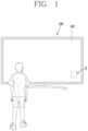
- FIG. 1 is a conceptual view illustrating one implementation of a display device using semiconductor light-emitting elements
- FIG. 2 is a partial enlarged view of the portion A in the display device of FIG. 1
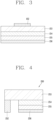
- FIG. 3 is an enlarged view of the semiconductor light-emitting element of FIG. 2
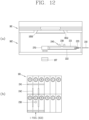
- FIG. 4 is an enlarged view illustrating another implementation of the semiconductor light-emitting element of FIG. 2 .
- information processed by a controller of a display device 100 may be output on a display module 140.
- a closed loop-shaped case that runs around the edge of the display module 140 may define the bezel of the display device.
- the display module 140 may include a panel 141 that displays an image, and the panel 141 may include micro-sized semiconductor light-emitting elements (or diodes) 150 and a wiring substrate 110 where the semiconductor light-emitting elements 150 are mounted.
- the panel 141 may include micro-sized semiconductor light-emitting elements (or diodes) 150 and a wiring substrate 110 where the semiconductor light-emitting elements 150 are mounted.
- the wiring substrate 110 may be provided with wirings, which can be connected to n-type electrodes 152 and p-type electrodes 156 of the semiconductor light-emitting elements 150.
- the semiconductor light-emitting elements 150 may be provided on the wiring substrate 110 as individual pixels that emit light on their own.
- the image displayed on the panel 141 may be visual information, which is rendered by controlling the light emission of unit pixels (sub-pixels) arranged in a matrix configuration independently through the wirings.
- microLEDs light-emitting diodes
- the microLEDs may be light-emitting elements that are small in size less than 100 ⁇ m.
- the semiconductor light-emitting elements 150 may have light-emitting regions of red, green, and blue, and unit pixels may be produced by combinations of these colors. That is, the unit pixels are the smallest units for producing one color.
- Each unit pixel may contain at least three microLEDs.
- the semiconductor light-emitting element 150 may have a vertical structure.
- the semiconductor light-emitting elements 150 may be implemented as high-power light-emitting elements that are composed mostly of gallium nitride (GaN), with some indium (In) and/or aluminum (Al) added to it, and emit light of various colors.
- GaN gallium nitride
- Al aluminum
- Such a vertical semiconductor light-emitting element may include a p-type electrode 156, a p-type semiconductor layer 155 disposed on the p-type semiconductor layer 156, an active layer 154 disposed on the p-type semiconductor layer 155, an n-type semiconductor layer 153 disposed on the active layer 154, and an n-type electrode 152 disposed on the n-type semiconductor layer 153.
- the p-type electrode 156 at the bottom may be electrically connected to a p-electrode of the wiring substrate, and the upper n-type electrode 152 at the top may be electrically connected to an n-electrode above the semiconductor light-emitting element.
- the electrodes can be disposed in an upward/downward direction in the vertical semiconductor light-emitting element 150, thereby providing a great advantage of reducing a chip size.
- the semiconductor light-emitting elements may be flip chip-type light-emitting elements.
- the semiconductor light-emitting element 250 may include a p-type electrode 256, a p-type semiconductor layer 255 disposed on the p-type layer 256, an active layer 254 disposed on the p-type semiconductor layer 255, an n-type semiconductor layer 253 disposed on the active layer 254, and an n-type electrode 252 vertically separated from the p-type electrode 256 on the n-type semiconductor layer 253.
- both the p-type electrode 256 and the n-type electrode 252 may be electrically connected to a p electrode and an n electrode of the wiring substrate, below the semiconductor light-emitting element.
- the vertical semiconductor light-emitting element and a horizontal light-emitting element each may be used as a green semiconductor light-emitting element, blue semiconductor light-emitting element, or red semiconductor light-emitting element.
- the green semiconductor light-emitting element and the blue semiconductor light-emitting element may be implemented as high-power light-emitting elements that are composed mostly of gallium nitride (GaN), with some indium (In) and/or aluminum (Al) added to it, and emit green and blue light, respectively.
- the semiconductor light-emitting elements may be made of gallium nitride thin films which include various layers of n-Gan, p-GaN, AlGaN, InGaN, etc.
- the p-type semiconductor layer may be P-type GaN, and the n-type semiconductor layer may be N-type GaN.
- the p-type semiconductor layer may be P-type GaAs, and the n-type semiconductor layer may be N-type GaAs.
- the p-type semiconductor layer may be P-type GaN doped with Mg on the p electrode
- the n-type semiconductor layer may be N-type GaN doped with Si on the n electrode.
- the above-described semiconductor light-emitting elements may be semiconductor light-emitting elements without the active layer.
- self-emissive, high-definition unit pixels may be arranged on the display panel, and therefore the display device can deliver high picture quality.
- semiconductor light-emitting elements may be grown on a wafer, formed through mesa and isolation, and used as individual pixels.
- the micro-sized semiconductor light-emitting elements 150 should be transferred onto a wafer, at preset positions on a substrate of the display panel.
- One of the transfer technologies available may be pick and place, but it has a low success rate and requires a lot of time.
- a number of diodes may be transferred at a time by using a stamp or roll, which, however, is not suitable for large-screen displays because of limited yields.
- the present disclosure proposes a new method and device for manufacturing a display device that can solve these problems.
- FIGS. 5A to 5E are conceptual views illustrating a new process for manufacturing the semiconductor light-emitting elements (or diodes).
- a first conductive semiconductor layer 153, an active layer 154, and a second conductive semiconductor layer 155 may be grown on a growth substrate 159 ( FIG. 5A ).
- the active layer 154 may be grown on the first conductive semiconductor layer 153 and then the second conductive semiconductor layer 155 may be grown on the active layer 154.
- the first conductive semiconductor layer 153, the active layer 154, and the second conductive semiconductor layer 155 may form a stack structure as illustrated in FIG. 5A .
- the first conductive semiconductor layer 153 may be a p-type semiconductor layer
- the second conductive semiconductor layer 155 may be an n-type semiconductor layer.
- the present disclosure is not necessarily limited to this, and the first conductive type may be n-type and the second conductive type may be p-type.
- the active layer may be omitted, if necessary, as stated above.
- the p-type semiconductor layer may be P-type GaN doped with Mg
- the n-type semiconductor layer may be N-type GaN doped with Si on the n electrode.
- the growth substrate 159 may be formed of, but not limited to, light-transmissive material, for example, one of sapphire (Al2O3), GaN, ZnO, and AlO. Also, the growth substrate 159 may be made of a material suitable for growing semiconductor materials, namely, a carrier wafer.
- the growth substrate 159 may be formed of a high thermal conducting material, and may be a conductive substrate or insulating substrate, for example, may use at least one of SiC, Si, GaAs, GaP, InP, and Ga2O3 substrates which have higher thermal conductivity than sapphire (Al2O3) substrates.
- a plurality of semiconductor light-emitting elements may be formed by removing at least parts of the first conductive semiconductor layer 153, the active layer 154, and the second conductive semiconductor layer 155 ( FIG. 5B ).
- isolation may be performed so that the plurality of light-emitting elements form a light-emitting diode array. That is, a plurality of semiconductor light-emitting elements may be formed by vertically etching the first conductive semiconductor layer 153, the active layer 154, and the second conductive semiconductor layer 155.
- a mesa process may be performed which exposes the first conductive semiconductor layer 153 to the outside by vertically removing part of the active layer 154 and the second conductive semiconductor layer 155, and then isolation may be performed which forms an array of semiconductor light-emitting elements by etching the first conductive semiconductor layer 153.
- a second conductive electrode 156 (or p-type electrode) may be formed on one surface of the second conductive semiconductor layer 155 ( FIG. 5C ).
- the second conductive electrode 156 may be formed by a deposition method such as sputtering, but the present disclosure is not necessarily limited to this.
- the second conductive electrode 156 may serve as an n-type electrode.
- the growth substrate 159 may be removed, thus leaving a plurality of semiconductor light-emitting elements.
- the growth substrate 159 may be removed using laser lift-off (LLO) or chemical lift-off (CLO) ( FIG. 5D ).
- the step of mounting the semiconductor light-emitting elements 150 on a substrate161 in a chamber filled with a fluid may be performed ( FIG. 5E ).
- the semiconductor light-emitting elements 150 and the substrate 161 may be put into a chamber filled with a fluid, and the semiconductor light-emitting elements may be self-assembled onto the substrate 161 using fluidity, gravity, surface tension, etc.
- the substrate may be an assembly substrate 161.
- a wiring substrate instead of the assembly substrate 161, may be put into a fluid chamber, and the semiconductor light-emitting elements 150 may be mounted directly onto the wiring substrate.
- the substrate may be a wiring substrate.
- the present disclosure is illustrated with an example in which the semiconductor light-emitting elements 150 are mounted onto the assembly substrate 161.
- cells into which the semiconductor light-emitting elements 150 are fitted may be provided on the assembly substrate 161.
- cells where the semiconductor light-emitting elements 150 are mounted may be disposed on the assembly substrate 161 at positions where the semiconductor light-emitting elements 150 are aligned with wiring electrodes.
- the semiconductor light-emitting elements 150 may be assembled to the cells as they move within the fluid.
- the semiconductor light-emitting elements 150 may be transferred to the wiring substrate from the assembly substrate 161, thereby enabling a large-area transfer across a large area.
- the assembly substrate 161 may be referred to as a temporary substrate.
- the present disclosure proposes a method and device that minimizes the effects of gravity or friction and avoids non-specific binding, in order to increase the transfer yield.
- a magnetic material may be placed on the semiconductor light-emitting elements so that the semiconductor light-emitting elements are moved by magnetic force, and the semiconductor light-emitting elements may be mounted at preset positions by an electric field in the process of being moved.
- FIG. 6 is a conceptual diagram illustrating an example of a device for self-assembling semiconductor light-emitting elements and FIG. 7 is a block diagram of the self-assembly device of FIG. 6 .
- FIGS. 8A to 8E are conceptual view illustrating a process for self-assembling semiconductor light-emitting elements using the self-assembly device of FIG. 6 and
- FIG. 9 is a conceptual view illustrating the semiconductor light-emitting element of FIGS. 8A to 8E .
- the self-assembly device 160 may include a fluid chamber 162, a magnet 163, and a position controller 164.
- the fluid chamber 162 may define a space for receiving a plurality of semiconductor light-emitting elements.
- the space may be filled with a fluid, and the fluid may be an assembly solution, which includes water or the like.
- the fluid chamber 162 may be a water tank and configured as an open-type.
- the present disclosure is not limited to this, and the fluid chamber 162 may be a closed-type chamber in which the space is in a closed state.
- a substrate 161 may be placed in the fluid chamber 162 so that an assembly surface where the semiconductor light-emitting elements 150 are assembled faces downwards.
- the substrate 161 may be fed to an assembly site by a feed unit (transfer unit), and the transfer unit may include a stage 165 where the substrate is mounted.
- the position of the stage 165 may be adjusted by the controller, whereby the substrate 161 can be fed to the assembly site.
- the assembly surface of the substrate 161 at the assembly site may face the bottom of the fluid chamber 162.
- the assembly surface of the substrate 161 may be placed to be soaked with the fluid in the fluid chamber 162.
- the semiconductor light-emitting elements 150 in the fluid may be moved to the assembly surface.
- the substrate 161 may be an assembly substrate where an electric field can be formed, and may include a base portion 161a, a dielectric layer 161b, and a plurality of electrodes 161c.
- the base portion 161a may be made of an insulating material, and the plurality of electrodes 161c may be thin-film or thick-film bi-planar electrodes that are patterned on one surface of the base portion 161a.
- the electrodes 161c may be formed of a stack of Ti/Cu/Ti, Ag paste, ITO, etc.
- the dielectric layer 161b may be made of an inorganic material such as SiO2, SiNx, SiON, Al2O3, TiO2, HfO2, etc.
- the dielectric layer 161b may be an organic insulator and configured as a single layer or multi-layers.
- the thickness of the dielectric layer 161b may range from several tens of nm to several ⁇ m.
- the substrate 161 may include a plurality of cells 161d that are separated by barrier walls (or partition parts) 161e.
- the cells 161d may be sequentially arranged in one direction and made of polymer material.
- the barrier walls 161e defining the cells 161d may be shared by neighboring cells 161d.
- the barrier walls 161e may protrude from the base portion 161a, and the cells 161d may be sequentially arranged in one direction along the barrier walls 161e. More specifically, the cells 161d may be sequentially arranged in column and row directions and have a matrix configuration.
- the cells 161d may have recesses for receiving the semiconductor light-emitting elements 150, and the recesses may be spaces defined by the barrier walls 161e.
- the recesses may have a shape identical or similar to the shape of the semiconductor light-emitting elements. For example, if the semiconductor light-emitting elements are rectangular, the recesses may be rectangular too.
- the recesses formed in the cells may be circular if the semiconductor light-emitting diodes are circular.
- each cell may be configured to receive one semiconductor light-emitting element. That is, one cell may receive one semiconductor light-emitting element.
- the plurality of electrodes 161c may have a plurality of electrode lines that are placed at the bottom of the cells 161d, and the electrode lines may extend to neighboring cells.
- the plurality of electrodes 161c may be placed beneath the cells 161d, and different polarities may be applied to create an electric field within the cells 161d.
- the dielectric layer 161b may form the bottom of the cells 161d while covering the electrodes 161c.
- the electrodes of the substrate 161 at the assembly site may be electrically connected to a power supply 171.
- the power supply 171 may perform the function of generating the electric field by applying power to the electrodes.
- the self-assembly device may have the magnet 163 for applying magnetic force to the semiconductor light-emitting elements.
- the magnet 163 may be disposed at a distance from the fluid chamber 162 to apply magnetic force to the semiconductor light-emitting elements 150.
- the magnet 163 may be disposed to face an opposite side of the assembly surface of the substrate 161, and the position of the magnet 163 may be controlled by the position controller 164 connected to the magnet 163.
- the semiconductor light-emitting elements 1050 may have a magnetic material so that they can be moved within the fluid by a magnetic field.
- a semiconductor light-emitting element having a magnetic material may include a first conductive electrode 1052, a second conductive electrode 1056, a first conductive semiconductor layer 1053 on which the first conductive electrode 1052 is disposed, a second conductive semiconductor layer 1055 which overlaps the first conductive semiconductor layer 1052 and on which the second conductive electrode 1056 is disposed, and an active layer 1054 disposed between the first and second conductive semiconductor layers 1053 and 1055.
- the first conductive may refer to p-type
- the second conductive type may refer to n-type, or vice versa.
- the semiconductor light-emitting diode may be formed without the active layer.
- the first conductive electrode 1052 may be formed after the semiconductor light-emitting element is assembled onto the wiring substrate by the self-assembling of the semiconductor light-emitting element.
- the second conductive electrode 1056 may include a magnetic material.
- the magnetic material may refer a magnetic metal.
- the magnetic material may be Ni, SmCo, etc.
- the magnetic material may include at least one of Gd-based, La-based, and Mn-based materials.
- the magnetic material may be provided in the form of particles on the second conductive electrode 1056.
- one layer of a conductive electrode including a magnetic material may be made of the magnetic material.
- the second conductive electrode 1056 of the semiconductor light-emitting element 1050 may include a first layer 1056a and a second layer 1056b, as illustrated in FIG. 9 .
- the first layer 1056a may include a magnetic material
- the second layer 1056b may include a metal material other than the magnetic material.
- the first layer 1056a including the magnetic material may be disposed in contact with the second conductive semiconductor layer 1055.
- the first layer 1056a may be disposed between the second layer 1056b and the second conductive semiconductor layer 1055.
- the second layer 1056b may be a contact metal that is connected to the second electrode on the wiring substrate.
- the present disclosure is not necessarily limited to this, and the magnetic material may be disposed on one surface of the first conductive semiconductor layer.
- a magnet handler capable of automatically or manually moving the magnet 163 on the x, y, and z axes or a motor capable of rotating the magnet 163 may be provided.
- the magnet handler and motor may constitute the position controller 164.
- the magnet 163 may rotate in a horizontal, clockwise, or counterclockwise direction with respect to the substrate 161.
- the fluid chamber 162 may be provided with a light-transmissive bottom plate 166, and the semiconductor light-emitting elements may be disposed between the bottom plate 166 and the substrate 161.
- An image sensor 167 may be disposed to face the bottom plate 166 so as to monitor the inside of the fluid chamber 162 through the bottom plate 166.
- the image sensor 167 may be controlled by a controller 172, and may include an inverted-type lens, CCD, etc. so as to observe the assembly surface of the substrate 161.
- the self-assembly device may be configured to use a magnetic field and an electric field in combination.
- the semiconductor light-emitting elements can be mounted at preset positions on the substrate by the electric field while being moved by changes in the position of the magnet.
- the assembly process using the self-assembly device will be described in more detail.
- a plurality of semiconductor light-emitting elements 1050 having a magnetic material may be formed through the process explained with reference to FIGS. 5A to 5C .
- the magnetic material may be deposited onto the semiconductor light-emitting elements in the process of forming the second conductive electrode of FIG. 5C .
- the substrate 161 may be fed to an assembly site, and the semiconductor light-emitting elements 1050 may be put into the fluid chamber 162 ( FIG. 8A ).
- the assembly site on the substrate 161 may be a position at which the substrate 161 is placed in the fluid chamber 162 in such a way that an assembly surface where the semiconductor light-emitting elements 150 are assembled faces downwards.
- some of the semiconductor light-emitting elements 1050 may sink to the bottom of the fluid chamber 162 and some of them may float in the fluid.
- some of the semiconductor light-emitting elements 1050 may sink to the bottom plate 166.
- magnetic force may be applied to the semiconductor light-emitting elements 1050 so that the semiconductor light-emitting elements 1050 in the fluid chamber 162 come up to the surface ( FIG. 8B ).
- the semiconductor light-emitting elements 1050 may float in the fluid towards the substrate 161.
- the original position may refer to s position at which the magnet 163 is outside the fluid chamber 162.
- the magnet 163 may be configured as an electromagnet. In this case, an initial magnetic force may be generated by supplying electricity to the electromagnet.
- the spacing between the assembly surface of the substrate 161 and the semiconductor light-emitting elements 1050 may be controlled by adjusting strength of the magnetic force.
- the spacing may be controlled by using weight, buoyancy, and magnetic force of the semiconductor light-emitting elements 1050.
- the spacing may be several millimeters to several tens of micrometers from the outermost part of the substrate 161.
- magnetic force may be applied to the semiconductor light-emitting elements 1050 so that the semiconductor light-emitting elements 1050 can move in one direction within the fluid chamber 162.
- the magnet 163 may move in a horizontal direction to the substrate, a clockwise direction, or a counterclockwise direction ( FIG. 8C ).
- the semiconductor light-emitting elements 1050 may be moved horizontally with respect to the substrate 161 by the magnetic force, with being spaced apart from the substrate 161.
- the semiconductor light-emitting elements 1050 may be guided to preset positions on the substrate 161 by applying an electric field so that the semiconductor light-emitting elements 1050 are mounted at the preset positions during their movement ( FIG. 8C ).
- the semiconductor light-emitting elements 1050 may be moved vertically with respect to the substrate 161 by the electric field while being moved horizontally with respect to the substrate 161, thereby being placed at the preset positions of the substrate 161.
- an electric field may be generated by supplying power to bi-planar electrodes on the substrate 161, and the semiconductor light-emitting electrodes 1050 may be guided to be assembled only at the preset positions by the electric field. That is, the semiconductor light-emitting elements 1050 may be self-assembled at the assembly site on the substrate 161 by a selectively generated electric field.
- the substrate 161 may be provided with cells into which the semiconductor light-emitting elements 1050 are fitted.
- the substrate 161 is an assembly substrate
- the assembled semiconductor light-emitting elements may be transferred onto a wiring substrate to carry out a subsequent process for realizing the display device, as described previously.
- the magnet 163 may be moved away from the substrate 161 such that the semiconductor light-emitting elements 1050 remaining in the fluid chamber 162 fall to the bottom of the fluid chamber 162 ( FIG. 8D ).
- the semiconductor light-emitting elements 1050 remaining in the fluid chamber 162 may fall to the bottom of the fluid chamber 162.
- the semiconductor light-emitting elements 1050 on the bottom of the fluid chamber 162 may be collected, and the collected semiconductor light-emitting elements 1050 may be re-used.
- parts at far distances may be concentrated near a preset assembly site by using a magnetic field in order to increase assembly yields in a fluidic assembly, and guided to be selectively assembled only at the assembly site by applying an electric field to the assembly site.
- the assembly substrate may be positioned on top of a water tank, with its assembly surface facing downward, thereby minimizing the effect of gravity from the weights of the parts and avoiding non-specific binding and eliminating defects. That is, the assembly substrate may be placed on the top to increase transfer yields, thus minimizing the effect of gravity or friction and avoiding non-specific binding.
- a large number of semiconductor light-emitting elements can be pixelated on a small-sized wafer and then transferred onto a large-area substrate. This enables the manufacture of a large-area display device at a low cost.
- FIG. 10 is a view illustrating mis-assembly types upon self-assembly.
- the semiconductor light-emitting elements 1050 are normally assembled by being placed at preset positions of the assembly substrate 161, i.e., in the cells 161d, by the self-assembly process described above ((d) of FIG. 10 ). However, some semiconductor light-emitting elements 1050 have failed to be accurately fitted in the cells 161d due to being caught on the barrier walls 161e surrounding the cells 161d in the process of being placed in the cells 161d ((a) of FIG.
- the semiconductor light-emitting elements 1050 for the self-assembly have a structure in which selectivity of an assembling direction is secured by a difference in surface area. A surface with a wide surface area is generally placed in contact with the bottom surface of the cell 161d, but in some cases, the semiconductor light-emitting element 1050 may be assembled in an opposite direction ((d) of FIG. 10 ).
- the present disclosure proposes a module for removing mis-assembled semiconductor light-emitting elements (hereinafter, referred to as a removal module) considering specificity of self-assembly in a fluid, and a method for removing a mis-assembled semiconductor light-emitting element using the same.
- a removal module a module for removing mis-assembled semiconductor light-emitting elements (hereinafter, referred to as a removal module) considering specificity of self-assembly in a fluid, and a method for removing a mis-assembled semiconductor light-emitting element using the same.
- FIG. 11 is a view illustrating a removal module in accordance with one implementation
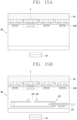
- FIG. 12 is a view illustrating a removal module applied to a self-assembly device (fluid chamber)
- FIG. 13 is a view illustrating a removal module in accordance with an exemplary variation
- FIG. 14 is a view illustrating a removal module to which a color filter or a metal thin film layer is applied.
- a removal module 200 may be used to remove the semiconductor light-emitting element 1050, which is mis-assembled on the assembly substrate 161, as illustrated in FIG. 10 , after the semiconductor light-emitting elements 1050 introduced into a fluid filled in the chamber 162 are self-assembled into the cells 161d arranged in the matrix form on the assembly substrate 161 by using an electric field and a magnetic field.
- the removal module 200 may be disposed in the fluid chamber 162 to remove the mis-assembled semiconductor light-emitting element 1050 from the assembly substrate 161 in a manner of spraying (injecting) a fluid on a position of the mis-assembled semiconductor light-emitting element 1050.
- the removal module 200 may include a fluid supply unit 210 for supplying a fluid and a housing 220.
- the fluid supply unit 210 may be connected to one side of the housing 220 to supply a fluid to an inner space 224 of the housing 220.
- the fluid supply unit 210 may be a fluid supply tube, and one end may be connected to the housing 220 through a joint portion 223 disposed at the one side of the housing 220 and another end may be connected to a fluid pump so as to receive a fluid to supply to the housing 220.
- the housing 220 may include an inner space 224 in which the fluid supplied from the fluid supply unit 210 can temporarily stay, an upper plate 221 disposed at a side adjacent to the assembly substrate 161, and a lower plate 222 disposed at a side adjacent to a bottom surface of the fluid chamber 162.
- the housing 220 may have an integral form or may be formed by coupling detachable components.
- the upper plate 221 and the lower plate 222 may be made of a transparent material such as glass or silicon, such that an alignment of the removal module 200 and a removal of a mis-assembled semiconductor light-emitting element 1050 can be monitored in real time through the image sensor 167 disposed below the fluid chamber 162, as illustrated in FIG. 6 .
- a separate sensor may be additionally disposed to monitor the alignment of the removal module 200 and the mis-assembled state of the semiconductor light-emitting element 1050.
- a nozzle hole 230 through which the inner space 224 of the housing 220 and an inner space of the chamber 162 communicate with each other may be formed through the upper plate 221.
- the nozzle hole 230 may spray (inject) the fluid supplied from the fluid supply unit 210 to a mis-assembly site of the semiconductor light-emitting element 1050 on the assembly substrate 161, so that the mis-assembled semiconductor light-emitting element 1050 can be removed from the assembly substrate 161.
- the nozzle hole 230 may not be limited to any shape like a circular hole, a slit hole, etc., but may have a shape with its width that is uniform or getting narrow in an upward direction, as illustrated, depending on a material of the upper plate 221 or a process.
- a pair of barrier walls (or partition parts) 240 facing each other based on the nozzle hole 230 may be disposed on the upper plate 221.
- the barrier walls 240 may be disposed near the nozzle hole 230, to block the fluid sprayed through the nozzle hole 230 from sputtering to regions adjacent to the mis-assembly site and thus prevent the affection of the fluid to the normally-assembled semiconductor light-emitting elements 1050.
- the barrier walls 240 may include first barrier walls 241 and second barrier walls 242. Specifically, the barrier walls 240 may include a pair of first barrier walls 241 extending in a row direction of the semiconductor light-emitting elements 1050 arranged in the matrix configuration on the assembly substrate 161, and a pair of second barrier walls 242 extending in a column direction.
- the semiconductor light-emitting elements 1050 may be arranged in a plurality of rows and columns on the assembly substrate 161, and may be arranged at intervals of several tens to several hundreds of ⁇ m along the plurality of rows and columns.
- the semiconductor light-emitting elements 1050 may be arranged in the row direction at intervals of several tens of ⁇ m, and may be arranged in the column direction at intervals of several hundreds of ⁇ m.
- the first barrier walls 241 may have an interval which is equal to or narrower than an interval between the semiconductor light-emitting elements 1050 in the column direction and the second barrier walls 242 may have an interval equal to or narrower than an interval between the semiconductor light-emitting elements 1050 in the row direction.
- the interval between the semiconductor light-emitting elements 1050 in the column or row direction may refer to a distance between centers of two adjacent semiconductor light-emitting elements 1050 in the column or row direction. That is, the first barrier walls 241 and the second barrier walls 242 may isolate the mis-assembly site from regions adjacent to the semiconductor light-emitting elements 1050 arranged in the row or column direction. Accordingly, a region, which is affected by the fluid sprayed through the nozzle hole 230 surrounded by the first barrier walls 241 and the second barrier walls 242, can be limited to the mis-assembly site.
- first barrier walls 241 extending along the row direction of the semiconductor light-emitting element 1050 may extend longer than at least a length of the cell 161d in the row direction in which the semiconductor light-emitting element 1050 is fitted.
- the second barrier walls 242 extending along the column direction of the semiconductor light-emitting element 1050 may extend longer than at least a length of the cell 161d in the column direction in which the semiconductor light-emitting element 161d is fitted. This can prevent the fluid sprayed through the nozzle hole 230 from sputtering to the semiconductor light-emitting elements 1050 normally assembled in the adjacent cells 161d.
- the removal module 200 may include a transfer unit 270 for position alignment.
- the transfer unit 270 may move the housing 220 in horizontal and vertical directions so that the removal module 200 correspond to a position of the semiconductor light-emitting element 1050 which is mis-assembled on the assembly substrate 161.
- the transfer unit 270 may be a general configuration used to align positions of equipment, and may include, for example, a transfer rail, a motor, and the like.
- the housing 220 may be horizontally moved on a virtual plane parallel to the assembly substrate 161 by the transfer unit 270 to be first aligned below the mis-assembly site and vertically moved close to the assembly substrate 161 to be finally aligned. Details regarding the alignment of the removal module 200 will be described later.
- air bubbles may be introduced into the inner space 224 of the housing 220 in the process of initially setting the removal module 220 in the chamber 162 and in the process of receiving the fluid.
- the introduced air bubbles may interfere with a smooth process of removing the mis-assembled semiconductor light-emitting element 1050 using the removal module 200.
- the upper plate 221 may have a modified structure as illustrated in FIG. 13 to remove air bubbles introduced into the housing 220.
- the upper plate 221 may include a first surface 221a facing the assembly substrate 161 and a second surface 221b facing the inner space 224 of the housing 220.
- the second surface 221b may have a convex shape toward the first surface 221a. That is, one surface of the upper plate 221 facing the inner space 224 of the housing 220 may be curved.
- the nozzle hole 230 may allow the inner space 224 of the housing 220 and the inner space of the fluid chamber 162 to communicate with each other through the highest point of the second surface 221b.
- the structure may guide the air bubbles distributed in the housing 220 toward the highest point of the second surface 221b, so that the air bubbles can be removed together when the fluid is sprayed through the nozzle hole 230.
- the nozzle hole 230 may be formed in a size smaller than a size of the semiconductor light-emitting element 1050 which is several to several tens of ⁇ m, which causes a limit to accurately arranging the nozzle hole 230 at the mis-assembly site. In particular, it is more difficult to accurately align the nozzle hole 230 when the upper plate 221 is formed of a transparent material.
- the upper plate 221 may further include a color filter 250 or a metal thin film layer 260.
- the color filter 250 may be disposed on the upper plate 221 and a fine hole (not shown) may be formed at a position corresponding to the nozzle hole 230.
- the color filter 250 may be disposed on the upper plate 221 such that the fine hole (not shown) formed through the color filter 250 and the nozzle hole 230 formed through the upper plate 221 overlap each other.
- the nozzle hole 230 can be distinguished from a peripheral region, which is identified by a specific color, by the fine hole (not shown), and the fluid sprayed through the nozzle hole 230 can spray onto the mis-assembly site via the fine hole (not shown) of the color filter 250.
- the metal thin film layer 260 may be formed in a sputtering manner along a circumference of the nozzle hole 230 formed through the upper plate 221.
- the nozzle hole 230 may be easily identified by the colored metal thin film layer 260.
- the upper plate 221 may include both the color filter 250 and the metal thin film layer 260.
- the color filter 250 and the metal thin film layer 260 may be formed at either a surface of the upper plate 221 facing the assembly substrate 161 or a surface facing the inner space 224 of the housing 220.
- the color filter 250 and the metal thin film layer 260 may preferably be formed at the surface facing the assembly plate 161.
- the removal module 200 can be disposed in the fluid chamber 162 to selectively remove the mis-assembled semiconductor light-emitting element 1050 by spraying a fluid onto a specific site of the assembly substrate 161, on which the semiconductor light-emitting elements 1050 having a size of several to several tens of ⁇ m are arranged at intervals of several tens to several hundreds of ⁇ m by the self-assembly.
- the semiconductor light-emitting elements 1050 normally assembled at the adjacent regions can be prevented from being separated by the fluid sprayed through the nozzle hole 230.
- the upper plate 221 has the convex surface, air bubbles generated in the housing 220 can also be removed through the nozzle hole 230 when spraying the fluid.
- the color filter 250 or the metal thin film layer 260 can be provided to facilitate identification of the fine nozzle hole 230, such that the nozzle hole 230 can be aligned at an accurate position.
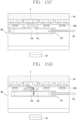
- FIGS. 15A to 15E are conceptual diagrams illustrating a method for removing a mis-assembled semiconductor light-emitting element using a removal module according to an implementation.
- a process for removing a mis-assembled semiconductor light-emitting element is a process performed after self-assembly is completed.
- the self-assembly means placing the semiconductor light-emitting elements 1050 introduced into the fluid in preset positions of the assembly substrate 161, namely, in the cells 161d using an electric field and a magnetic field.
- the semiconductor light-emitting elements 1050 floating in the fluid may be moved into the cells 161d by an electric field and a magnetic field applied from the assembly substrate 161 and the upper side of the assembly substrate 161. In this process, some semiconductor light-emitting elements 1050 may not be assembled normally as illustrated in FIG. 10 .
- the present disclosure relates to a method for removing a semiconductor light-emitting element 1050 mis-assembled on the assembly substrate 161 using the removal module 200.
- a method for removing a semiconductor light-emitting element 1050 mis-assembled on the assembly substrate 161 using the removal module 200 will be described in detail.
- an image or a video of one surface of the completely self-assembled assembly substrate 161 (a surface facing the bottom surface of the fluid chamber 162 and having the semiconductor light-emitting element 1050 placed thereon) may be captured using the image sensor 167 disposed outside the fluid chamber 162. Whether there is a mis-assembled semiconductor light-emitting element and coordinates of a position of the mis-assembled semiconductor light-emitting element 1050 may be checked from the image or video.
- mis-assembly site X For example, in the case of FIG. 15A , presence of a semiconductor light-emitting element 1050 that has been placed in a different direction may be identified on the captured image or video, and coordinates of the corresponding cell (hereinafter, mis-assembly site X) can also be identified.
- the cells 161d on which the semiconductor light-emitting elements 1050 are placed may be formed in the matrix configuration on the assembly substrate 161, and the semiconductor light-emitting elements 1050 may be arranged in the matrix configuration on the assembly substrate 161. Therefore, the coordinates of the position of the mis-assembly site X can be indicated by coordinates (x, y) of row and column.
- the removal module 200 may be put into the fluid chamber 162, to be located below a point corresponding to the identified coordinates of the position, as illustrated in FIGS. 15B and 15C .
- the removal module 200 may be moved horizontally and vertically to be aligned at a position for spraying the fluid.
- the removal module 200 may be horizontally moved so that the position coordinates (x, y) of the nozzle hole 230 of the removal module 200 for spraying the fluid and the mis-assembly site X correspond to each other.
- Horizontal movement may mean movement on a virtual horizontal plane (xy plane) parallel to the assembly substrate 161, and horizontal movement may correspond to movement for aligning the position of the mis-assembly site X and the position of the removal module 200.
- the vertical movement of the removal module 200 may be made.
- the vertical movement may be movement to make one end of each barrier wall 240 of the removal module 200 closer to one surface of the assembly substrate 161, and may be continued until the one end of each barrier wall 240 is in contact with or adjacent to the assembly substrate 161.
- the mis-assembly site X may be isolated from adjacent regions by the barrier walls 240, and a region affected by the fluid injected through the nozzle hole 230 may be limited to a region surrounded by the barrier walls 240.
- the fluid may be sprayed on the mis-assembled position of the semiconductor light-emitting element 1050, namely, the mis-assembly site X, to remove the mis-assembled semiconductor light-emitting element 1050 from the assembly substrate 161.
- the fluid can be sprayed through the nozzle hole 230 toward an arbitrary region within the mis-assembly site X, for example, on a gap defined between the semiconductor light-emitting element 1050 and the cell 161d.
- the semiconductor light-emitting element 1050 When the mis-assembled semiconductor light-emitting element 1050 is removed from the assembly substrate 161 through those steps ( FIG. 15E ), the semiconductor light-emitting element 1050 may be re-assembled to the corresponding position.
- a single or two or more removal modules 200 may be used to remove the mis-assembled semiconductor light-emitting elements 1050.
- the removal module 200 may identify coordinates of positions of a plurality of mis-assembly sites X obtained from a captured image or video, calculate a shortest path based on the respective coordinates, and move along the calculated shortest path.
- the removal modules 200 may be located below the plurality of mis-assembly sites X, respectively, spray the fluid simultaneously onto the mis-assembly sites X, and remove the mis-assembled semiconductor light-emitting elements 1050.
- the plurality of removal modules 200 may be provided in the same number as the number of mis-assembly sites X.
- those removal modules 200 may be arranged below arbitrary mis-assembly sites X in consideration of a shortest path calculated from coordinates of the mis-assembly sites X.
- the step of removing the semiconductor light-emitting elements 1050 mis-assembled on the assembly substrate 161 can be performed, thereby securing a process yield for manufacturing a display device.
Landscapes
- Led Device Packages (AREA)
- Led Devices (AREA)
Claims (12)
- Modul zum Entfernen eines fehlmontierten lichtausstrahlenden Halbleiterelements (1050) aus einem Montagesubstrat (161), wobei das fehlmontierte lichtausstrahlende Halbleiterelement (1050) in ein in einer Kammer (162) aufgenommenes Fluid eingesetzt wurde und auf dem Montagesubstrat (161) unter Verwendung eines elektrischen Felds und eines Magnetfelds selbst-montiert wurde, wobei das Modul aufweist:eine Fluidzuleitungseinheit (210), die eingerichtet ist, Fluid zuzuleiten; undein Gehäuse, das einen Innenraum (224) hat, der eingerichtet ist, das von der Fluidzuleitungseinheit (210) zugeleitete Fluid aufzubewahren, wobei das Gehäuse eine obere Platte (221) aufweist, die eingerichtet ist, dem Montagesubstrat (161) zugewandt zu sein und aufweist:eine Düsenöffnung (230), die eingerichtet ist, das von der Fluidzuleitungseinheit (210) zugeleitete Fluid in Richtung des fehlmontierten lichtausstrahlenden Halbleiterelements (1050) auf dem Montagesubstrat zu sprühen; unddas Modul dadurch gekennzeichnet ist, dass es weiterhin aufweistwenigstens ein Paar von Trennteilen oder Sperrwänden (420), wobei die Düsenöffnung (230) dazwischen angeordnet ist.
- Modul nach Anspruch 1, wobei das wenigstens eine Paar von Trennteilen (240) aufweist:ein Paar von ersten Trennteilen (241), die parallel zu einer Zeilenrichtung von lichtausstrahlenden Halbleiterelementen (1050) verlaufen, die auf dem Montagesubstrat (161) angeordnet sind; undein Paar von zweiten Trennteilen (242), die parallel zu einer Spaltenrichtung der lichtausstrahlenden Halbleiterelemente (1050) verlaufen, die auf dem Montagesubstrat (161) angeordnet sind.
- Modul nach Anspruch 2, wobei ein erster Trennabstand des Paars der ersten Trennteile (241) kleiner oder gleich einem Intervallabstand zwischen den entlang der Spaltenrichtung angeordneten lichtausstrahlenden Halbleiterelementen (1050) ist und ein zweiter Trennabstand des Paars von zweiten Trennteilen (242) kleiner oder gleich einem Intervallabstand zwischen den entlang der Zeilenrichtung angeordneten lichtausstrahlenden Halbleiterelementen (1050) ist.
- Modul nach Anspruch 2, wobei ein jedes von dem Paar von ersten Trennteilen (241) länger als wenigstens eine Länge einer Zelle des Montagesubstrats (161) in der Zeilenrichtung verläuft, und ein jedes von dem Paar von zweiten Trennteilen (242) länger als wenigstens eine Länge der Zelle (161d) des Montagesubstrats (161) in der Spaltenrichtung verläuft.
- Modul nach Anspruch 1, wobei die obere Platte (221) weiterhin aufweist:eine Innenfläche, die dem Innenraum (224) des Gehäuses (220) zugewandt ist und eine konkave Fläche hat,wobei die Düsenöffnung (230) am höchsten Punkt der konkaven Fläche positioniert ist.
- Modul nach Anspruch 1, wobei die obere Platte (221) weiterhin einen Farbfilter (250) aufweist, der eine feine Öffnung hat, die an einer Position entsprechend der Düsenöffnung ausgebildet ist.
- Modul nach Anspruch 1, wobei die obere Platte (221) weiterhin eine dünne Metallfolienschicht (260) aufweist, die entlang einem Umfang der Düsenöffnung (230) ausgebildet ist.
- Modul nach Anspruch 1, das weiterhin eine Übertragungseinheit (270) aufweist, die eingerichtet ist, das Gehäuse (220) zu übertragen, um einer Position des falsch montierten lichtausstrahlenden Halbleiterelements (1050) zu entsprechen.
- Verfahren zum Entfernen eines fehlmontierten lichtausstrahlenden Halbleiterelements (1050) aus einem Montagesubstrat (161), wobei das fehlmontierte lichtausstrahlende Halbleiterelement (1050) in ein in einer Kammer (162) aufgenommenes Fluid eingesetzt wurde und auf dem Montagesubstrat (161) unter Verwendung eines elektrischen Felds und eines Magnetfelds selbst-montiert wurde, wobei das Verfahren aufweist:Erfassen eines Bilds oder eines Videos des Montagesubstrats (161), auf dem die lichtausstrahlenden Halbleiterelemente (1050) montiert sind;Identifizieren der Koordinaten eines fehlmontierten lichtausstrahlenden Halbleiterelements (1050) basierend auf dem erfassten Bild oder Video;Ausrichten eines Entfernungsmoduls (200) an einer Position, die den identifizierten Koordinaten entspricht, wobei das Entfernungsmodul (200) eine Flüssigkeitszuleitungseinheit (210) aufweist, die ausgestaltet ist, Fluid zuzuleiten, einen Innenraum (224), der mit der Fluidzuleitungseinheit (210) verbunden ist, und eine obere Platte (221), die eingerichtet ist, dem Montagemodul zugewandt zu sein, wobei die obere Platte (221) aufweist: eine Düsenöffnung (230), die eingerichtet ist, das von der Fluidzuleitungseinheit (210) zugeleitete Fluid in Richtung des Montagesubstrats (161) zu sprühen, und wenigstens ein Paar von Trennteilen (420), wobei die Düsenöffnung (320) dazwischen angeordnet ist; undEntfernen des fehlmontierten lichtausstrahlenden Halbleiterelements (1050) aus dem Montagesubstrat (161) unter Verwendung des Entfernungsmoduls (200) durch Sprühen des Fluids in Richtung des fehlmontierten lichtausstrahlenden Halbleiterelements (1050).
- Verfahren nach Anspruch 9, wobei das Ausrichten des Entfernungsmoduls (200) an der Position entsprechend den identifizierten Koordinaten aufweist:seitliches Verschieben des Entfernungsmoduls (200), sodass die Düsenöffnung (230) sich an den identifizierten Koordinaten befindet; undVerschieben des Entfernungsmoduls (200) in Richtung des Montagesubstrats (161), sodass das wenigstens eine Paar von Trennelementen (240) nahe einer Fläche des Montagesubstrats (161) positioniert ist, um zu verhindern, dass das Fluid auf benachbarte lichtausstrahlende Halbleiterelemente (1050) gesprüht wird.
- Verfahren nach Anspruch 9, wobei basierend auf der Identifikation von mehreren Koordinaten, die einer Vielzahl von fehlmontierten lichtausstrahlenden Halbleiterelementen (1050) entsprechen, das Verfahren weiterhin das Berechnen eines kürzesten Wegs basierend auf Koordinaten von einem jeden von der Vielzahl der fehlmontierten lichtausstrahlenden Halbleiterelemente (1050) und das Verschieben des Entfernungsmoduls (200) entlang dem berechneten kürzesten Pfad aufweist.
- Verfahren nach Anspruch 9, wobei basierend auf der Identifikation von mehreren Koordinaten, die einer Vielzahl von fehlmontierten lichtausstrahlenden Halbleiterelementen (1050) entsprechen, das Verfahren weiterhin aufweist das Verschieben einer Vielzahl von Entfernungsmodulen (200), um an Positionen ausgerichtet zu sein, die jeweils den mehreren identifizierten Koordinaten entsprechen, um so gleichzeitig die Vielzahl der fehlmontierten lichtausstrahlenden Halbleiterelemente (1050) zu entfernen.
Applications Claiming Priority (1)
| Application Number | Priority Date | Filing Date | Title |
|---|---|---|---|
| PCT/KR2019/008798 WO2021010521A1 (ko) | 2019-07-16 | 2019-07-16 | 오조립된 반도체 발광소자의 제거 모듈 및 이를 이용한 오조립된 반도체 발광소자의 제거방법 |
Publications (3)
| Publication Number | Publication Date |
|---|---|
| EP4002440A1 EP4002440A1 (de) | 2022-05-25 |
| EP4002440A4 EP4002440A4 (de) | 2023-04-19 |
| EP4002440B1 true EP4002440B1 (de) | 2024-02-21 |
Family
ID=74210406
Family Applications (1)
| Application Number | Title | Priority Date | Filing Date |
|---|---|---|---|
| EP19938073.4A Active EP4002440B1 (de) | 2019-07-16 | 2019-07-16 | Modul zur entfernung eines falsch montierten lichtemittierenden elements und verfahren zur entfernung eines falsch montierten lichtemittierenden elements damit |
Country Status (3)
| Country | Link |
|---|---|
| US (1) | US12046484B2 (de) |
| EP (1) | EP4002440B1 (de) |
| WO (1) | WO2021010521A1 (de) |
Families Citing this family (4)
| Publication number | Priority date | Publication date | Assignee | Title |
|---|---|---|---|---|
| EP3817036A4 (de) | 2018-06-27 | 2022-03-23 | Samsung Display Co., Ltd. | Vorrichtung zur herstellung einer lichtemittierenden anzeigevorrichtung |
| KR102630588B1 (ko) * | 2018-09-21 | 2024-01-31 | 삼성디스플레이 주식회사 | 발광 표시 장치의 제조 장치 및 제조 방법 |
| US12368130B2 (en) | 2019-08-05 | 2025-07-22 | Lg Electronics Inc. | Module for removing misassembled semiconductor light-emitting element, and method using same to remove misassembled semiconductor light-emitting element |
| CN114725148A (zh) * | 2021-01-05 | 2022-07-08 | 群创光电股份有限公司 | 显示装置的制作方法 |
Family Cites Families (10)
| Publication number | Priority date | Publication date | Assignee | Title |
|---|---|---|---|---|
| US5355577A (en) | 1992-06-23 | 1994-10-18 | Cohn Michael B | Method and apparatus for the assembly of microfabricated devices |
| JP4396285B2 (ja) | 2004-01-21 | 2010-01-13 | ソニー株式会社 | 素子配列基板および素子配列方法 |
| US10446728B2 (en) * | 2014-10-31 | 2019-10-15 | eLux, Inc. | Pick-and remove system and method for emissive display repair |
| US9892944B2 (en) | 2016-06-23 | 2018-02-13 | Sharp Kabushiki Kaisha | Diodes offering asymmetric stability during fluidic assembly |
| US10543486B2 (en) * | 2014-10-31 | 2020-01-28 | eLux Inc. | Microperturbation assembly system and method |
| US10418527B2 (en) * | 2014-10-31 | 2019-09-17 | eLux, Inc. | System and method for the fluidic assembly of emissive displays |
| KR102568252B1 (ko) * | 2016-07-21 | 2023-08-22 | 삼성디스플레이 주식회사 | 발광 장치 및 그의 제조방법 |
| JP2018041876A (ja) | 2016-09-08 | 2018-03-15 | スタンレー電気株式会社 | 発光装置の製造方法及び発光装置 |
| KR102268048B1 (ko) | 2019-07-11 | 2021-06-22 | 엘지전자 주식회사 | 오조립된 반도체 발광소자의 제거 모듈 및 이를 이용한 오조립된 반도체 발광소자의 제거방법 |
| US12368130B2 (en) * | 2019-08-05 | 2025-07-22 | Lg Electronics Inc. | Module for removing misassembled semiconductor light-emitting element, and method using same to remove misassembled semiconductor light-emitting element |
-
2019
- 2019-07-16 WO PCT/KR2019/008798 patent/WO2021010521A1/ko not_active Ceased
- 2019-07-16 EP EP19938073.4A patent/EP4002440B1/de active Active
- 2019-07-16 US US17/627,110 patent/US12046484B2/en active Active
Also Published As
| Publication number | Publication date |
|---|---|
| US12046484B2 (en) | 2024-07-23 |
| WO2021010521A1 (ko) | 2021-01-21 |
| EP4002440A1 (de) | 2022-05-25 |
| US20220254657A1 (en) | 2022-08-11 |
| EP4002440A4 (de) | 2023-04-19 |
Similar Documents
| Publication | Publication Date | Title |
|---|---|---|
| EP3731276B1 (de) | Vorrichtung und verfahren zur selbstmontage eines lichtemittierenden halbleiterbauelements | |
| KR102888284B1 (ko) | 반도체 발광소자를 이용한 디스플레이 장치 | |
| KR102726299B1 (ko) | 반도체 발광소자를 이용한 디스플레이 장치 및 이의 제조방법 | |
| US20230119947A1 (en) | A substrate for manufacturing display device and a manufacturing method using the same | |
| US12324292B2 (en) | Apparatus and method for self-assembly of semiconductor light-emitting element | |
| KR102145192B1 (ko) | 반도체 발광 소자를 이용한 디스플레이 장치 및 이의 제조방법 | |
| KR102162739B1 (ko) | 반도체 발광소자의 자가조립 장치 및 방법 | |
| US11869871B2 (en) | Apparatus and method for self-assembling semiconductor light-emitting device | |
| EP4030481B1 (de) | Anzeigevorrichtung mit lichtemittierender halbleiterdiode | |
| EP4002440B1 (de) | Modul zur entfernung eines falsch montierten lichtemittierenden elements und verfahren zur entfernung eines falsch montierten lichtemittierenden elements damit | |
| KR102268048B1 (ko) | 오조립된 반도체 발광소자의 제거 모듈 및 이를 이용한 오조립된 반도체 발광소자의 제거방법 | |
| EP4105970A1 (de) | Vorrichtung und verfahren zur selbstmontage einer lichtemittierenden halbleitervorrichtung | |
| EP4024440A1 (de) | Vorrichtung und verfahren zum sammeln von lichtemittierenden halbleiterdioden | |
| US12080689B2 (en) | Display device using semiconductor light-emitting elements and manufacturing method therefor | |
| US20230031398A1 (en) | Display device using semiconductor light-emitting element, and manufacturing method therefor | |
| US20230005888A1 (en) | Semiconductor light-emitting element supply device and supply method | |
| EP3975228B1 (de) | Modul zum entfernen eines falsch montierten lichtemittierenden halbleiterelements und verfahren zum entfernen eines falsch montierten lichtemittierenden halbleiterelements damit | |
| KR20220120642A (ko) | 반도체 발광소자를 이용한 디스플레이 장치의 제조방법 | |
| US20230317491A1 (en) | Apparatus and method for self-assembling semiconductor light emitting diodes | |
| US20230138887A1 (en) | Semiconductor light-emitting element collecting method and semiconductor light-emitting element collecting method using same | |
| US12469731B2 (en) | Method for manufacturing display device | |
| EP4105995B1 (de) | Anzeigevorrichtung mit verwendung von lichtemittierenden halbleiterelementen und verfahren zur herstellung davon | |
| US12080825B2 (en) | Method for manufacturing display device using semiconductor light emitting device | |
| US20230299055A1 (en) | Substrate for manufacturing display device, and method for manufacturing display device by using same |
Legal Events
| Date | Code | Title | Description |
|---|---|---|---|
| STAA | Information on the status of an ep patent application or granted ep patent |
Free format text: STATUS: THE INTERNATIONAL PUBLICATION HAS BEEN MADE |
|
| PUAI | Public reference made under article 153(3) epc to a published international application that has entered the european phase |
Free format text: ORIGINAL CODE: 0009012 |
|
| STAA | Information on the status of an ep patent application or granted ep patent |
Free format text: STATUS: REQUEST FOR EXAMINATION WAS MADE |
|
| 17P | Request for examination filed |
Effective date: 20220214 |
|
| AK | Designated contracting states |
Kind code of ref document: A1 Designated state(s): AL AT BE BG CH CY CZ DE DK EE ES FI FR GB GR HR HU IE IS IT LI LT LU LV MC MK MT NL NO PL PT RO RS SE SI SK SM TR |
|
| DAV | Request for validation of the european patent (deleted) | ||
| DAX | Request for extension of the european patent (deleted) | ||
| A4 | Supplementary search report drawn up and despatched |
Effective date: 20230317 |
|
| RIC1 | Information provided on ipc code assigned before grant |
Ipc: H01L 25/16 20060101ALI20230313BHEP Ipc: H01L 33/00 20100101ALI20230313BHEP Ipc: H01L 21/683 20060101ALI20230313BHEP Ipc: H01L 21/68 20060101ALI20230313BHEP Ipc: H01L 21/67 20060101ALI20230313BHEP Ipc: H01L 25/075 20060101ALI20230313BHEP Ipc: H01L 23/00 20060101AFI20230313BHEP |
|
| GRAP | Despatch of communication of intention to grant a patent |
Free format text: ORIGINAL CODE: EPIDOSNIGR1 |
|
| STAA | Information on the status of an ep patent application or granted ep patent |
Free format text: STATUS: GRANT OF PATENT IS INTENDED |
|
| RIC1 | Information provided on ipc code assigned before grant |
Ipc: H01L 25/16 20060101ALI20230825BHEP Ipc: H01L 33/00 20100101ALI20230825BHEP Ipc: H01L 21/683 20060101ALI20230825BHEP Ipc: H01L 21/68 20060101ALI20230825BHEP Ipc: H01L 21/67 20060101ALI20230825BHEP Ipc: H01L 25/075 20060101ALI20230825BHEP Ipc: H01L 23/00 20060101AFI20230825BHEP |
|
| RAP3 | Party data changed (applicant data changed or rights of an application transferred) |
Owner name: LG ELECTRONICS INC. |
|
| INTG | Intention to grant announced |
Effective date: 20230919 |
|
| GRAS | Grant fee paid |
Free format text: ORIGINAL CODE: EPIDOSNIGR3 |
|
| GRAA | (expected) grant |
Free format text: ORIGINAL CODE: 0009210 |
|
| STAA | Information on the status of an ep patent application or granted ep patent |
Free format text: STATUS: THE PATENT HAS BEEN GRANTED |
|
| AK | Designated contracting states |
Kind code of ref document: B1 Designated state(s): AL AT BE BG CH CY CZ DE DK EE ES FI FR GB GR HR HU IE IS IT LI LT LU LV MC MK MT NL NO PL PT RO RS SE SI SK SM TR |
|
| REG | Reference to a national code |
Ref country code: GB Ref legal event code: FG4D |
|
| REG | Reference to a national code |
Ref country code: CH Ref legal event code: EP |
|
| REG | Reference to a national code |
Ref country code: DE Ref legal event code: R096 Ref document number: 602019047148 Country of ref document: DE |
|
| REG | Reference to a national code |
Ref country code: IE Ref legal event code: FG4D |
|
| REG | Reference to a national code |
Ref country code: LT Ref legal event code: MG9D |
|
| REG | Reference to a national code |
Ref country code: NL Ref legal event code: MP Effective date: 20240221 |
|
| PG25 | Lapsed in a contracting state [announced via postgrant information from national office to epo] |
Ref country code: IS Free format text: LAPSE BECAUSE OF FAILURE TO SUBMIT A TRANSLATION OF THE DESCRIPTION OR TO PAY THE FEE WITHIN THE PRESCRIBED TIME-LIMIT Effective date: 20240621 |
|
| PG25 | Lapsed in a contracting state [announced via postgrant information from national office to epo] |
Ref country code: LT Free format text: LAPSE BECAUSE OF FAILURE TO SUBMIT A TRANSLATION OF THE DESCRIPTION OR TO PAY THE FEE WITHIN THE PRESCRIBED TIME-LIMIT Effective date: 20240221 |
|
| PG25 | Lapsed in a contracting state [announced via postgrant information from national office to epo] |
Ref country code: GR Free format text: LAPSE BECAUSE OF FAILURE TO SUBMIT A TRANSLATION OF THE DESCRIPTION OR TO PAY THE FEE WITHIN THE PRESCRIBED TIME-LIMIT Effective date: 20240522 |
|
| REG | Reference to a national code |
Ref country code: AT Ref legal event code: MK05 Ref document number: 1659863 Country of ref document: AT Kind code of ref document: T Effective date: 20240221 |
|
| PG25 | Lapsed in a contracting state [announced via postgrant information from national office to epo] |
Ref country code: NL Free format text: LAPSE BECAUSE OF FAILURE TO SUBMIT A TRANSLATION OF THE DESCRIPTION OR TO PAY THE FEE WITHIN THE PRESCRIBED TIME-LIMIT Effective date: 20240221 Ref country code: RS Free format text: LAPSE BECAUSE OF FAILURE TO SUBMIT A TRANSLATION OF THE DESCRIPTION OR TO PAY THE FEE WITHIN THE PRESCRIBED TIME-LIMIT Effective date: 20240521 Ref country code: HR Free format text: LAPSE BECAUSE OF FAILURE TO SUBMIT A TRANSLATION OF THE DESCRIPTION OR TO PAY THE FEE WITHIN THE PRESCRIBED TIME-LIMIT Effective date: 20240221 |
|
| PG25 | Lapsed in a contracting state [announced via postgrant information from national office to epo] |
Ref country code: ES Free format text: LAPSE BECAUSE OF FAILURE TO SUBMIT A TRANSLATION OF THE DESCRIPTION OR TO PAY THE FEE WITHIN THE PRESCRIBED TIME-LIMIT Effective date: 20240221 |
|
| PG25 | Lapsed in a contracting state [announced via postgrant information from national office to epo] |
Ref country code: AT Free format text: LAPSE BECAUSE OF FAILURE TO SUBMIT A TRANSLATION OF THE DESCRIPTION OR TO PAY THE FEE WITHIN THE PRESCRIBED TIME-LIMIT Effective date: 20240221 |
|
| PG25 | Lapsed in a contracting state [announced via postgrant information from national office to epo] |
Ref country code: RS Free format text: LAPSE BECAUSE OF FAILURE TO SUBMIT A TRANSLATION OF THE DESCRIPTION OR TO PAY THE FEE WITHIN THE PRESCRIBED TIME-LIMIT Effective date: 20240521 Ref country code: NO Free format text: LAPSE BECAUSE OF FAILURE TO SUBMIT A TRANSLATION OF THE DESCRIPTION OR TO PAY THE FEE WITHIN THE PRESCRIBED TIME-LIMIT Effective date: 20240521 Ref country code: NL Free format text: LAPSE BECAUSE OF FAILURE TO SUBMIT A TRANSLATION OF THE DESCRIPTION OR TO PAY THE FEE WITHIN THE PRESCRIBED TIME-LIMIT Effective date: 20240221 Ref country code: LT Free format text: LAPSE BECAUSE OF FAILURE TO SUBMIT A TRANSLATION OF THE DESCRIPTION OR TO PAY THE FEE WITHIN THE PRESCRIBED TIME-LIMIT Effective date: 20240221 Ref country code: IS Free format text: LAPSE BECAUSE OF FAILURE TO SUBMIT A TRANSLATION OF THE DESCRIPTION OR TO PAY THE FEE WITHIN THE PRESCRIBED TIME-LIMIT Effective date: 20240621 Ref country code: HR Free format text: LAPSE BECAUSE OF FAILURE TO SUBMIT A TRANSLATION OF THE DESCRIPTION OR TO PAY THE FEE WITHIN THE PRESCRIBED TIME-LIMIT Effective date: 20240221 Ref country code: GR Free format text: LAPSE BECAUSE OF FAILURE TO SUBMIT A TRANSLATION OF THE DESCRIPTION OR TO PAY THE FEE WITHIN THE PRESCRIBED TIME-LIMIT Effective date: 20240522 Ref country code: FI Free format text: LAPSE BECAUSE OF FAILURE TO SUBMIT A TRANSLATION OF THE DESCRIPTION OR TO PAY THE FEE WITHIN THE PRESCRIBED TIME-LIMIT Effective date: 20240221 Ref country code: ES Free format text: LAPSE BECAUSE OF FAILURE TO SUBMIT A TRANSLATION OF THE DESCRIPTION OR TO PAY THE FEE WITHIN THE PRESCRIBED TIME-LIMIT Effective date: 20240221 Ref country code: BG Free format text: LAPSE BECAUSE OF FAILURE TO SUBMIT A TRANSLATION OF THE DESCRIPTION OR TO PAY THE FEE WITHIN THE PRESCRIBED TIME-LIMIT Effective date: 20240221 Ref country code: AT Free format text: LAPSE BECAUSE OF FAILURE TO SUBMIT A TRANSLATION OF THE DESCRIPTION OR TO PAY THE FEE WITHIN THE PRESCRIBED TIME-LIMIT Effective date: 20240221 |
|
| PG25 | Lapsed in a contracting state [announced via postgrant information from national office to epo] |
Ref country code: PT Free format text: LAPSE BECAUSE OF FAILURE TO SUBMIT A TRANSLATION OF THE DESCRIPTION OR TO PAY THE FEE WITHIN THE PRESCRIBED TIME-LIMIT Effective date: 20240621 Ref country code: PL Free format text: LAPSE BECAUSE OF FAILURE TO SUBMIT A TRANSLATION OF THE DESCRIPTION OR TO PAY THE FEE WITHIN THE PRESCRIBED TIME-LIMIT Effective date: 20240221 |
|
| PG25 | Lapsed in a contracting state [announced via postgrant information from national office to epo] |
Ref country code: SE Free format text: LAPSE BECAUSE OF FAILURE TO SUBMIT A TRANSLATION OF THE DESCRIPTION OR TO PAY THE FEE WITHIN THE PRESCRIBED TIME-LIMIT Effective date: 20240221 Ref country code: PT Free format text: LAPSE BECAUSE OF FAILURE TO SUBMIT A TRANSLATION OF THE DESCRIPTION OR TO PAY THE FEE WITHIN THE PRESCRIBED TIME-LIMIT Effective date: 20240621 Ref country code: PL Free format text: LAPSE BECAUSE OF FAILURE TO SUBMIT A TRANSLATION OF THE DESCRIPTION OR TO PAY THE FEE WITHIN THE PRESCRIBED TIME-LIMIT Effective date: 20240221 Ref country code: LV Free format text: LAPSE BECAUSE OF FAILURE TO SUBMIT A TRANSLATION OF THE DESCRIPTION OR TO PAY THE FEE WITHIN THE PRESCRIBED TIME-LIMIT Effective date: 20240221 |
|
| PG25 | Lapsed in a contracting state [announced via postgrant information from national office to epo] |
Ref country code: DK Free format text: LAPSE BECAUSE OF FAILURE TO SUBMIT A TRANSLATION OF THE DESCRIPTION OR TO PAY THE FEE WITHIN THE PRESCRIBED TIME-LIMIT Effective date: 20240221 |
|
| PG25 | Lapsed in a contracting state [announced via postgrant information from national office to epo] |
Ref country code: SM Free format text: LAPSE BECAUSE OF FAILURE TO SUBMIT A TRANSLATION OF THE DESCRIPTION OR TO PAY THE FEE WITHIN THE PRESCRIBED TIME-LIMIT Effective date: 20240221 |
|
| PG25 | Lapsed in a contracting state [announced via postgrant information from national office to epo] |
Ref country code: CZ Free format text: LAPSE BECAUSE OF FAILURE TO SUBMIT A TRANSLATION OF THE DESCRIPTION OR TO PAY THE FEE WITHIN THE PRESCRIBED TIME-LIMIT Effective date: 20240221 Ref country code: EE Free format text: LAPSE BECAUSE OF FAILURE TO SUBMIT A TRANSLATION OF THE DESCRIPTION OR TO PAY THE FEE WITHIN THE PRESCRIBED TIME-LIMIT Effective date: 20240221 |
|
| PG25 | Lapsed in a contracting state [announced via postgrant information from national office to epo] |
Ref country code: SK Free format text: LAPSE BECAUSE OF FAILURE TO SUBMIT A TRANSLATION OF THE DESCRIPTION OR TO PAY THE FEE WITHIN THE PRESCRIBED TIME-LIMIT Effective date: 20240221 |
|
| PG25 | Lapsed in a contracting state [announced via postgrant information from national office to epo] |
Ref country code: SM Free format text: LAPSE BECAUSE OF FAILURE TO SUBMIT A TRANSLATION OF THE DESCRIPTION OR TO PAY THE FEE WITHIN THE PRESCRIBED TIME-LIMIT Effective date: 20240221 Ref country code: SK Free format text: LAPSE BECAUSE OF FAILURE TO SUBMIT A TRANSLATION OF THE DESCRIPTION OR TO PAY THE FEE WITHIN THE PRESCRIBED TIME-LIMIT Effective date: 20240221 Ref country code: RO Free format text: LAPSE BECAUSE OF FAILURE TO SUBMIT A TRANSLATION OF THE DESCRIPTION OR TO PAY THE FEE WITHIN THE PRESCRIBED TIME-LIMIT Effective date: 20240221 Ref country code: EE Free format text: LAPSE BECAUSE OF FAILURE TO SUBMIT A TRANSLATION OF THE DESCRIPTION OR TO PAY THE FEE WITHIN THE PRESCRIBED TIME-LIMIT Effective date: 20240221 Ref country code: DK Free format text: LAPSE BECAUSE OF FAILURE TO SUBMIT A TRANSLATION OF THE DESCRIPTION OR TO PAY THE FEE WITHIN THE PRESCRIBED TIME-LIMIT Effective date: 20240221 Ref country code: CZ Free format text: LAPSE BECAUSE OF FAILURE TO SUBMIT A TRANSLATION OF THE DESCRIPTION OR TO PAY THE FEE WITHIN THE PRESCRIBED TIME-LIMIT Effective date: 20240221 |
|
| REG | Reference to a national code |
Ref country code: DE Ref legal event code: R097 Ref document number: 602019047148 Country of ref document: DE |
|
| PG25 | Lapsed in a contracting state [announced via postgrant information from national office to epo] |
Ref country code: IT Free format text: LAPSE BECAUSE OF FAILURE TO SUBMIT A TRANSLATION OF THE DESCRIPTION OR TO PAY THE FEE WITHIN THE PRESCRIBED TIME-LIMIT Effective date: 20240221 |
|
| PLBE | No opposition filed within time limit |
Free format text: ORIGINAL CODE: 0009261 |
|
| STAA | Information on the status of an ep patent application or granted ep patent |
Free format text: STATUS: NO OPPOSITION FILED WITHIN TIME LIMIT |
|
| PG25 | Lapsed in a contracting state [announced via postgrant information from national office to epo] |
Ref country code: IT Free format text: LAPSE BECAUSE OF FAILURE TO SUBMIT A TRANSLATION OF THE DESCRIPTION OR TO PAY THE FEE WITHIN THE PRESCRIBED TIME-LIMIT Effective date: 20240221 |
|
| 26N | No opposition filed |
Effective date: 20241122 |
|
| PG25 | Lapsed in a contracting state [announced via postgrant information from national office to epo] |
Ref country code: MC Free format text: LAPSE BECAUSE OF FAILURE TO SUBMIT A TRANSLATION OF THE DESCRIPTION OR TO PAY THE FEE WITHIN THE PRESCRIBED TIME-LIMIT Effective date: 20240221 |
|
| REG | Reference to a national code |
Ref country code: CH Ref legal event code: PL |
|
| PG25 | Lapsed in a contracting state [announced via postgrant information from national office to epo] |
Ref country code: LU Free format text: LAPSE BECAUSE OF NON-PAYMENT OF DUE FEES Effective date: 20240716 |
|
| GBPC | Gb: european patent ceased through non-payment of renewal fee |
Effective date: 20240716 |
|
| PG25 | Lapsed in a contracting state [announced via postgrant information from national office to epo] |
Ref country code: LU Free format text: LAPSE BECAUSE OF NON-PAYMENT OF DUE FEES Effective date: 20240716 |
|
| PG25 | Lapsed in a contracting state [announced via postgrant information from national office to epo] |
Ref country code: SI Free format text: LAPSE BECAUSE OF FAILURE TO SUBMIT A TRANSLATION OF THE DESCRIPTION OR TO PAY THE FEE WITHIN THE PRESCRIBED TIME-LIMIT Effective date: 20240221 Ref country code: CH Free format text: LAPSE BECAUSE OF NON-PAYMENT OF DUE FEES Effective date: 20240731 Ref country code: BE Free format text: LAPSE BECAUSE OF NON-PAYMENT OF DUE FEES Effective date: 20240731 |
|
| PG25 | Lapsed in a contracting state [announced via postgrant information from national office to epo] |
Ref country code: GB Free format text: LAPSE BECAUSE OF NON-PAYMENT OF DUE FEES Effective date: 20240716 |
|
| REG | Reference to a national code |
Ref country code: BE Ref legal event code: MM Effective date: 20240731 |
|
| PGFP | Annual fee paid to national office [announced via postgrant information from national office to epo] |
Ref country code: FR Payment date: 20250611 Year of fee payment: 7 |
|
| PG25 | Lapsed in a contracting state [announced via postgrant information from national office to epo] |
Ref country code: IE Free format text: LAPSE BECAUSE OF NON-PAYMENT OF DUE FEES Effective date: 20240716 |
|
| PGFP | Annual fee paid to national office [announced via postgrant information from national office to epo] |
Ref country code: DE Payment date: 20250609 Year of fee payment: 7 |
|
| PG25 | Lapsed in a contracting state [announced via postgrant information from national office to epo] |
Ref country code: CY Free format text: LAPSE BECAUSE OF FAILURE TO SUBMIT A TRANSLATION OF THE DESCRIPTION OR TO PAY THE FEE WITHIN THE PRESCRIBED TIME-LIMIT; INVALID AB INITIO Effective date: 20190716 |
|
| REG | Reference to a national code |
Ref country code: DE Ref legal event code: R079 Ref document number: 602019047148 Country of ref document: DE Free format text: PREVIOUS MAIN CLASS: H01L0023000000 Ipc: H10W0099000000 |
|
| PG25 | Lapsed in a contracting state [announced via postgrant information from national office to epo] |
Ref country code: HU Free format text: LAPSE BECAUSE OF FAILURE TO SUBMIT A TRANSLATION OF THE DESCRIPTION OR TO PAY THE FEE WITHIN THE PRESCRIBED TIME-LIMIT; INVALID AB INITIO Effective date: 20190716 |