EP4004513B1 - Ein elastischer dreiachsiger kraftsensor und verfahren zur herstellung des gleichen - Google Patents
Ein elastischer dreiachsiger kraftsensor und verfahren zur herstellung des gleichen Download PDFInfo
- Publication number
- EP4004513B1 EP4004513B1 EP20746593.1A EP20746593A EP4004513B1 EP 4004513 B1 EP4004513 B1 EP 4004513B1 EP 20746593 A EP20746593 A EP 20746593A EP 4004513 B1 EP4004513 B1 EP 4004513B1
- Authority
- EP
- European Patent Office
- Prior art keywords
- sensor
- layer
- electrode layer
- force
- column electrodes
- Prior art date
- Legal status (The legal status is an assumption and is not a legal conclusion. Google has not performed a legal analysis and makes no representation as to the accuracy of the status listed.)
- Active
Links
Images




Classifications
-
- G—PHYSICS
- G01—MEASURING; TESTING
- G01L—MEASURING FORCE, STRESS, TORQUE, WORK, MECHANICAL POWER, MECHANICAL EFFICIENCY, OR FLUID PRESSURE
- G01L5/00—Apparatus for, or methods of, measuring force, work, mechanical power, or torque, specially adapted for specific purposes
- G01L5/16—Apparatus for, or methods of, measuring force, work, mechanical power, or torque, specially adapted for specific purposes for measuring several components of force
- G01L5/161—Apparatus for, or methods of, measuring force, work, mechanical power, or torque, specially adapted for specific purposes for measuring several components of force using variations in ohmic resistance
- G01L5/162—Apparatus for, or methods of, measuring force, work, mechanical power, or torque, specially adapted for specific purposes for measuring several components of force using variations in ohmic resistance of piezoresistors
-
- G—PHYSICS
- G01—MEASURING; TESTING
- G01L—MEASURING FORCE, STRESS, TORQUE, WORK, MECHANICAL POWER, MECHANICAL EFFICIENCY, OR FLUID PRESSURE
- G01L1/00—Measuring force or stress, in general
- G01L1/18—Measuring force or stress, in general using properties of piezo-resistive materials, i.e. materials of which the ohmic resistance varies according to changes in magnitude or direction of force applied to the material
-
- G—PHYSICS
- G01—MEASURING; TESTING
- G01L—MEASURING FORCE, STRESS, TORQUE, WORK, MECHANICAL POWER, MECHANICAL EFFICIENCY, OR FLUID PRESSURE
- G01L5/00—Apparatus for, or methods of, measuring force, work, mechanical power, or torque, specially adapted for specific purposes
- G01L5/0061—Force sensors associated with industrial machines or actuators
- G01L5/0076—Force sensors associated with manufacturing machines
- G01L5/009—Force sensors associated with material gripping devices
-
- G—PHYSICS
- G01—MEASURING; TESTING
- G01L—MEASURING FORCE, STRESS, TORQUE, WORK, MECHANICAL POWER, MECHANICAL EFFICIENCY, OR FLUID PRESSURE
- G01L5/00—Apparatus for, or methods of, measuring force, work, mechanical power, or torque, specially adapted for specific purposes
- G01L5/16—Apparatus for, or methods of, measuring force, work, mechanical power, or torque, specially adapted for specific purposes for measuring several components of force
-
- G—PHYSICS
- G01—MEASURING; TESTING
- G01L—MEASURING FORCE, STRESS, TORQUE, WORK, MECHANICAL POWER, MECHANICAL EFFICIENCY, OR FLUID PRESSURE
- G01L5/00—Apparatus for, or methods of, measuring force, work, mechanical power, or torque, specially adapted for specific purposes
- G01L5/22—Apparatus for, or methods of, measuring force, work, mechanical power, or torque, specially adapted for specific purposes for measuring the force applied to control members, e.g. control members of vehicles, triggers
- G01L5/226—Apparatus for, or methods of, measuring force, work, mechanical power, or torque, specially adapted for specific purposes for measuring the force applied to control members, e.g. control members of vehicles, triggers to manipulators, e.g. the force due to gripping
- G01L5/228—Apparatus for, or methods of, measuring force, work, mechanical power, or torque, specially adapted for specific purposes for measuring the force applied to control members, e.g. control members of vehicles, triggers to manipulators, e.g. the force due to gripping using tactile array force sensors
-
- A—HUMAN NECESSITIES
- A61—MEDICAL OR VETERINARY SCIENCE; HYGIENE
- A61B—DIAGNOSIS; SURGERY; IDENTIFICATION
- A61B2562/00—Details of sensors; Constructional details of sensor housings or probes; Accessories for sensors
- A61B2562/02—Details of sensors specially adapted for in-vivo measurements
- A61B2562/0252—Load cells
-
- A—HUMAN NECESSITIES
- A61—MEDICAL OR VETERINARY SCIENCE; HYGIENE
- A61B—DIAGNOSIS; SURGERY; IDENTIFICATION
- A61B2562/00—Details of sensors; Constructional details of sensor housings or probes; Accessories for sensors
- A61B2562/02—Details of sensors specially adapted for in-vivo measurements
- A61B2562/0285—Nanoscale sensors
-
- A—HUMAN NECESSITIES
- A61—MEDICAL OR VETERINARY SCIENCE; HYGIENE
- A61B—DIAGNOSIS; SURGERY; IDENTIFICATION
- A61B2562/00—Details of sensors; Constructional details of sensor housings or probes; Accessories for sensors
- A61B2562/04—Arrangements of multiple sensors of the same type
- A61B2562/046—Arrangements of multiple sensors of the same type in a matrix array
Definitions
- the present invention relates to a compliant tri-axial force sensor and method of fabricating such a sensor.
- force is a vector with two components, its magnitude as well as direction.
- Directional information/data has been of high interest in improving robotics for many years.
- a sensor that can determine both magnitude and direction is usually referred to as a tri-axial force sensor.
- These force torque (F/T) sensors are largely used as part of a robotic end-effector arm (see reference 1 listed at the end of the description), or more recently to measure the force directional components on robot finger-tips (see reference 2 listed at the end of the description).
- Many attempts have historically been made for such sensors, the more recent ones of which have achieved relatively high densities, however they have been made using solid-state materials and/or micromachining techniques.
- Some recent e-skins and data gloves have been made with the ability to give multiple points or high density tactile information (see references 3 and 4 listed at the end of the description), however most cannot give directional information which is crucial to measuring many phenomena. It can enable robots to grasp objects, detect their mass in a gravitational environment such as the earth, but also, for example, to measure ground reaction force in insoles for gait analysis, among other physical phenomena.
- piezoelectric sensing see reference 9 listed at the end of the description
- detection see reference 10 listed at the end of the description
- EMC electromagnetic compatibility
- magnetic sensing including the hall-effect and inductive methods
- references 11 to 14 listed at the end of the description is also affected by background EMC and surrounding magnetic fields, some of which could be created by the robot's own actuators.
- Quantum tunnelling materials as well as piezoresistive composites have been used before, but none of the systems proposed have been highly integratable or wrappable.
- Often flexible wiring is not flexible or compliant enough, either due to the material being too rigid or compliant in only 1-axis, or the layers not being thin-enough.
- the architecture for such a device usually involves the placement of a 'bump' that translated force into torque being placed directly above 4 orthogonally arranged pressure sensors or pressure sensing pixels (sensels). When the post experiences a force from a given direction at its tip, this gets translated into downwards force as well as a sideways torque. Consequently, the 4 pressure sensors experience different forces/pressures.
- Measuring the quantity of resistance change on each of these sensors can then be used to dissect the force into its 3D Cartesian components ( F x , F y and F z ).
- Various electrode configurations may be used for reading out the signal from the piezoresistive material (see reference 16 listed at the end of the description).
- piezoresistive tri-axial sensor arrays include an interlocked structure with sidewalls embedded in polydimethylsiloxane (PDMS) and a micro-pyramidal array structure (see reference 17 listed at the end of the description).
- PDMS polydimethylsiloxane
- micro-pyramidal array structure see reference 17 listed at the end of the description.
- the former has the advantage of being able to be deployed in relatively dense 3x3 arrays, however only works at very low loads of 0-225Pa.
- the latter has the advantage of having a wide dynamic range from 128Pa to 44kPa.
- it needs a high quantity of wiring as it is not amenable to be deployed as a matrix, while also having an overall structure which is several millimetres thick, meaning it cannot be wrapped around surfaces, and due to its complexity, mass-production would be very difficult.
- Quantum Tunnelling Composite materials were discovered in 1996 by David Lussey. They are composite materials composed essentially of metal particles as well as a non-conducting elastomeric binder or matrix. These materials have a very high resistance to electrical current, and are essentially insulators, when no pressure is applied. Once pressure is applied, their resistance drops exponentially, and this can be measured using the correct electrical circuitry. The reason for this is that the metal particles are dispersed in the material at a particular concentration, but are not in physical contact with one another. Upon the application of pressure, the metal particles approach each together, and despite not being able to touch each other, electrons begin to be able to jump from one particle to another through a phenomenon known as quantum tunnelling.
- particles are usually micrometre or nanometre sized and made up of a conductive material, typically a metal such as silver, gold, or magnetite. They are also often nano-patterned, and for example 'spiky' nanoparticles show better tunnelling behaviour than round ones, as the tips of the microscopic spikes enhance tunnelling current even if particles are at a higher distance from each other. This enhances sensitivity and overall performance.
- QTC ® pills supplied by Peratech have been used in an attempt to make tri-axial sensors but these devices suffer from miniaturization and other issues such as sensor hysteresis.
- QTC ® pills lack the ability to be integrated during a mass manufacturing process and are bulky in both thickness and minimum diameter, making them cumbersome and not particularly sensitive.
- Tri-axial sensors can be created (in research labs) using multiple transduction mechanisms such as: piezoresistive (e.g. using strain gauges or nanocomposites); capacitive; piezoelectric; inductive; optical; or magnetic. Piezoresistive and capacitive sensors dominate due to their excellent performance. However, capacitive sensors can be sensitive to the substrate they are placed on due to capacitive coupling with this surface, and require much more complex readout electronics which is a hindrance due to space requirements and implementation complexity.
- US2019/004651A1 discloses a display device including: a display panel including a plurality of pixels disposed in a display region; a pressure sensor disposed to overlap with the display panel, the pressure sensor including a plurality of sensor electrodes disposed in a touch region; a bump structure disposed on at least one of a first surface and a second surface of the pressure sensor to be separated from the sensor electrodes; and a housing supporting the display panel, the pressure sensor, and the bump structure.
- the bump structure includes a plurality of bumps distributed on respective coordinate points at which the sensor electrodes are disposed.
- a compliant tri-axial force sensor as defined in claim 1.
- embodiments of the invention comprise a compliant tri-axial force sensor which can be made of thin material layers allowing it to be fully compliant and flexible but which includes one or more spacers to maintain a spacing between certain layers such that the bending of the sensor will not itself cause erroneous force readings and the sensor can therefore be robust, reliable and repeatable.
- the sensor can tolerate thousands to millions of cycles without failing, and can therefore effectively operate in an industrial setting.
- a consistent output also eliminates significant time which may otherwise be required to calibrate each sensing element individually.
- the sensing elements per tactel (tactile element), i.e. bump.
- the sensor has a low susceptibility to background noise and can be easily configured for different force sensing ranges depending on the application (i.e. by increasing or decreasing the active layer thickness).
- the senor may be configured to be a thin, stretchable, conformable, nanocomposite-based tactile device which can measure force in three different axes (x, y and z).
- Embodiments of the invention may be compliant-enough to be wrapped around extremely small bending radii or soft robots, and nonetheless have a minimal effect on signal integrity or response allowing an accurate measurement of force magnitude as well as direction. Accordingly, the sensor performance is insensitive to bending.
- Flexible connections and electrical wiring is integrated into the sensor via the layer and electrode structure, and it has a 'bump' layer on top which translates force into torque.
- the senor is amenable to mass-production using any of a number of existing facile volume manufacturing processes such as screen printing and roll-to-roll printing using customizable materials whilst maintaining high yield.
- it can be deployed in large-scale arrays such as may be required for an electronic skin application.
- the sensor is highly integratable into different devices, products or garments and can be retro-fittable onto hard, soft, and stretchable surfaces.
- environmentally friendly materials may be employed.
- Each layer may be printed (e.g. by screen printing or inkjet printing) allowing it to be highly miniaturisable (at least to an ideal 1mm by 1mm tri-axis pixel density desired for a robotic end-effector).
- the first and/or second electrode layer may be formed from a conductive ink deposited on a layer below.
- the active layer may comprise at least one of: a quantum tunneling material, a piezoresistive material or a piezoelectric material.
- the at least one property that may change when the active is subjected to a force is the amount of: quantum tunnelling; conductivity; resistivity or electrical charge.
- embodiments of the invention may employ a composite material that utilises a quantum tunnelling conduction mechanism or piezoresistive conduction mechanism to translate applied force into a sensed signal.
- the active layer is conveniently anisotropic such that it reacts more selectively to normal forces when deposited in a thin layer, due to the material properties.
- the at least one three dimensional bump has a footprint which extends at least partially over at least two column electrodes in the first electrode layer and at least partially over at least two column electrodes in the second electrode layer such that forces applied to the bump are transmittable through the active layer in at least four discrete regions.
- each tactel tactel
- sensels sensing elements
- the strength of the force at each sensel can be used to determine both the magnitude and direction of the applied force (i.e. resulting in a combination of shear and compressive forces).
- the at least one three dimensional bump has a footprint contained within a space between two column electrodes in the first electrode layer and between two column electrodes in the second electrode layer.
- one or more spacers can be employed to redistribute the force applied to the bump to each of the 4 sensels (sensing elements).
- the active layer may comprise a first active layer and a second active layer with a gap there-between.
- the sensor may comprise one or more of: a base layer below the first electrode layer; a top layer above the second electrode layer; a first carbon layer between the first electrode layer and the active layer; a second carbon layer between the second electrode layer and the active layer; and a cover layer over the at least one three dimensional bump.
- the first and/or second carbon layer may be continuous across multiple column electrodes in the first and/or second electrode layer.
- the at least one spacer may be provided within the active layer; between the base layer and the top layer; or on or through the first or second electrode layer.
- the at least one spacer may be in the form of a dot, a column, a post, a cylinder, a tubular, a pyramid or a mesh.
- the at least one spacer may have a solid or hollow transverse cross-section in the form of a circle, square, rectangle, diamond, pentagon, hexagon or honeycomb lattice.
- the sensor may comprise an array of said spacers.
- the spacers in the array may have a plurality of different dimensions.
- the active layer may form a continuous layer across multiple column electrodes in the first and/or second electrode layer.
- the active layer may form a discontinuous layer across the column electrodes in the first and/or second electrode layer.
- the sensor may comprise an insulator between adjacent electrodes in the first and/or second electrode layer.
- the at least one spacer may take the form of a binder provided between the active layer and the first and/or second electrode layer, wherein the binder is provided in gaps between adjacent column electrodes and extends between the active layer and respective edges of said adjacent column electrodes.
- the sensor may comprise an adhesive layer provided between one or more adjacent layers.
- the at least one three dimensional bump may comprise a polymer having a different elasticity to a remainder of the sensor.
- the at least one three dimensional bump may be in the form of a mesa, dome, hemisphere, hemispherical section, cone, cone section, cuboid, cylinder, half-cylinder, pyramid, pyramid section, tetrahedron, tetrahedron section, hexahedron, triangular prism, polyhedron, or other shape.
- the at least one three dimensional bump may have a height that is at least twice a height of a remainder of the sensor.
- the bumps may be significantly taller than the remainder of the sensor (e.g. up to 3mm in height) in order to translate shear forces into a high enough torque, which in turn compresses the active layer material underneath with different pressures.
- Spacing between the tactels and sensels can be very low to increase resolution (e.g. 500 ⁇ m or below), as long as they are not touching and tunnelling cannot occur between them. Separating electrodes in this way helps to reduce cross-talk in the sensor.
- the sensor may comprise an array of said three dimensional bumps.
- embodiments of this aspect of the invention provide a method fabricating a sensor which can easily be mass-produced using a variety of existing techniques.
- Each layer, bump or spacer may be provided by one of: printing; screen-printing, roll-to-roll printing, inkjet printing, 3D printing, electrospinning, depositing, droplet dispensing, casting, coating, moulding, spinning or weaving.
- the method may comprise forming at least the first electrode layer and the second electrode layer on a single substrate; separating the substrate into two parts; and stacking the two parts together.
- the method may comprise forming the at least one spacer on at least one part prior to said separating and/or stacking.
- a compliant tri-axial force sensor 100 including four three dimensional dome-shaped bumps 102 in accordance with a first embodiment of the invention.
- the sensor 100 comprises a base layer 104 in the form of a bottom membrane encapsulation layer; a first (bottom) electrode layer 106 having an array of column electrodes 106a in a first orientation; a second (top) electrode layer 108 having an array of column electrodes 108a in a second orientation, which is orthogonal to the first orientation; a force-dependent active layer 110 in the form of a quantum tunneling material layer, which is configured to change at least one property when subjected to a force and which is provided between the first electrode layer 106 and the second electrode layer 108; and a top layer 112 in the form of a top membrane encapsulation layer.
- the dome-shaped bumps 102 are provided on the top layer and are arranged to transmit externally applied force through the active layer 110.
- at least one spacer is provided which is arranged to maintain a separation between two or more layers in the sensor 100 until an external force is applied. The spacers will be described in more detail below in relation to Fig.'s 4 through 11C.
- each bump 102 has a circular base 102a and curved sidewalls 102b which extend to a flattened top 102c.
- each of the base layer 104, the first electrode layer 106, the active layer 110, the second electrode layer 108 and the top layer 112 are 0.10mm thick forming a sensor body of 0.50mm thick.
- each column electrode 106a, 108a is 1mm wide and each bump 102 is 1mm in height and has a maximum diameter footprint of 3mm. There is a 1mm gap between each adjacent bump 102.
- the sensor body will usually be formed of relatively thin layers to allow the sensor to be compliant and to be capable of being applied to curved or other shaped surfaces.
- the bumps 102 may be significantly taller than the sensor body in order to translate shear forces into a high enough torque, which in turn compresses the active layer 110 underneath with different pressures.
- each three dimensional dome-shaped bump 102 has a footprint which extends at least partially over at least two column electrodes in the first electrode layer 106 and at least partially over at least two column electrodes in the second electrode layer 108 such that forces applied to the bump 102 are transmittable through the active layer 110 in at least four discrete regions.
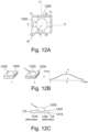
- each bump 102 can be considered as a tactile element (tactel) which is connected to four sensing elements (sensels) or pixels and the strength of the force at each sensel can be used to determine the position, magnitude and direction of the applied force (i.e. resulting in a combination of shear and compressive forces) as will be explained further below, with reference to Fig.'s12A, B and C.
- the column electrodes 106a, 108a are shown in dashed lines as if the layers of the sensor 100 are transparent.
- the sensor 100 is shown with an array of four bumps 102, the sensor body may be extended and may comprise any number of bumps 102 as required for any given application.
- the senor may be formed from any selection of the materials listed below.
- the base layer 104 and top layer 106 may be formed from any suitable substrate material and may comprise one or more of Poly(para-xylelene) polymers (Parylene), 2,8-Dichlorotricyclo[8.2.2.2 4,7 ]hexadeca-1(12),4,6,10,13,15-hexaene (Parylene-C), Polydimethylsiloxane (PDMS), Polyimide (PI), polybutyrate adipate terephthalate (polybutyrate), Poly(methyl methacrylate) (PMMA/Acrylic), prop-2-enoates (acrylate), polyethylene (PE), High-density polyethylene (HDPE), Low-density polyethylene (LDPE), Polyethylene Terephthalate (PET), Thermoplastic Polyurethane (TPU), Polyurethane (PU), Polysiloxanes (Silicone), Polyvinyl Chloride (PVC), Polyethyleneimine (PEI), Polyethylene Naphthalate (PEN), Polypropy
- Low Young's modulus polymers may help to attain higher conformability, such as those polymers having a Young's modulus of up to 1.5 MPa (Mega-Pascals), more preferably up to 1.2 MPa, still more preferably up to 1 MPa and preferably at least 500 kPa, such as in the range 700 kPa to 1 MPa, e.g. 700 to 800 kPa.
- Many more rigid polymers in the list e.g. PEN) are highly flexible at a thickness of e.g. 25 microns. Some example thicknesses for different possible substrates are: Parylene-C, 500-10000nm; PEN, 25-100 microns; PET, 36-125 microns; Silicone, 5-500 microns; and TPU, 50-75 microns
- the column electrodes 106a, 108a of both the first electrode layer 106 and the second electrode layer 108 may be formed of a conductive composite material such as an ink containing metal filler particles (micro or nanoscale). Carbon, silver, gold, and copper are the most commonly used. Metal thin-film (e.g. gold/copper) can be used if the substrate is not stretchable or particularly thin, or if the metal has tortuosity to bend while the substrate is being stretched, instead of stretching the metal itself. All of these need to be highly conductive, and the best metal to be used is gold due to it being the most malleable and ductile of all metals.
- a conductive composite material such as an ink containing metal filler particles (micro or nanoscale). Carbon, silver, gold, and copper are the most commonly used.
- Metal thin-film e.g. gold/copper
- All of these need to be highly conductive, and the best metal to be used is gold due to it being the most malleable and ductile of all metals.
- conductive inks by Engineered Materials Solutions, Inc. (EMS) (e.g. CI-1036 which is a silver conductive ink having a sheet resistivity of ⁇ 0.010 ⁇ /square at 25.4 microns thickness; or CI-2051 which is a carbon-based conductive ink having a sheet resistivity of ⁇ 50 ⁇ /square at 25.4 microns thickness).
- CI-1036 which is a silver conductive ink having a sheet resistivity of ⁇ 0.010 ⁇ /square at 25.4 microns thickness
- CI-2051 which is a carbon-based conductive ink having a sheet resistivity of ⁇ 50 ⁇ /square at 25.4 microns thickness
- Other suitable materials include Asahi TM ink and gold thin-film which has a resistivity of ⁇ 2.44 x 10 -8 ⁇ m at 20 degrees Celsius.
- the active layer 110 may comprise a quantum tunneling material, a piezoresistive material or a piezoelectric material.
- the quantum tunnelling material will exhibit an exponential decrease in resistance due to quantum tunnelling which leads to a massive resistance change up to 10 12 ⁇ , spanning a very large dynamic force range.
- the force range that can be sensed can be as low as 0.003N up to 200N and if more rigid materials are used in the sensor this could be expanded higher.
- An example of a suitable quantum tunneling material is Quantum Tunneling Composite (QTC ® ) which comprises a binder material plus nickel or silicon (semiconductor) filler particles with high aspect ratio tips (e.g. circular, spiky, or needle-like).
- Particles composed of dielectric materials such as titanium dioxide or fumed silica particles may also be used in the material.
- Metal or metal-alloys having a void bearing structure may also be used along with various different binders.
- Another suitable quantum tunneling material is QTSS ® which contains spiky or acicular magnetite and/or nickel particles and polyurethane binder. The particles do not touch each other but current can pass through them by means of the mechanism of quantum tunnelling.
- Zero dimension, one dimension, or two dimension nanoparticle materials may be desirable due to their enhanced dynamic range and sensitivity. Part of the reason for this may be due to local concentration of electric fields at their tips enhancing quantum tunnelling as well as a lower percolation threshold (and hence quantity) of the materials required.
- quantum tunnelling materials are most sensitive to compressive pressure between the electrodes measuring the resistance, which allows significant selectivity not provided by, for example, strain gauges. Quantum tunnelling materials are also less sensitive to temperature and environmental electromagnetic compatibility noise than many other sensors and materials.
- Suitable piezoresistive materials include nanocomposites and electrospun micro or nanofibers. Piezoresistive materials modulate current flow when a potential different is applied across them and pressure is applied to the material. These comprise an active filler (micro/nanoparticle) which may be carbon, carbon nanotube (CNT), multi-walled carbon nanotube (MWCNT), graphene, Borophene, silver, quantum dots, or any other electrically conductive or semiconductor micro/nanoparticles. They may also comprise surfactants which are usually functionalised on the surface of the nanoparticles to increase dispersion and reduce agglomeration due to e.g. Van der Waals forces.
- an active filler micro/nanoparticle
- CNT carbon nanotube
- MWCNT multi-walled carbon nanotube
- surfactants which are usually functionalised on the surface of the nanoparticles to increase dispersion and reduce agglomeration due to e.g. Van der Waals forces.
- a binder is also employed such as PDMS, silicone, tetrafluoroethylene (TFE), Propylene, PVDF (which is not piezoelectric in all its states), other polymers such as the ones contained in the substrate or concrete.
- the polymers can be thermosetting (i.e. undergo a permanent cross-linking reaction due to heat, moisture, light, or air) or non-thermosetting (i.e. melting). They can also be fluoropolymers.
- the piezoresistive materials may also comprise a solvent to control viscosity (e.g. during printing) but which is usually mostly evaporated away in air or while curing.
- the nanoparticles are ideally vertically aligned (and well dispersed) in order to enhance the anisotropic behaviour of the material to sense pressure in the normal direction with minimal pressure readout due to the material flexing and stretching.
- Some particles in the piezoresistive material may be electrically or magnetically aligned (by application of a static or varying electric and/or magnetic field across the materials before and/or during curing and/or deposition). For example, this can be done using dielectrophoretic alignment by varying an AC (alternating current) electric field through the material before curing, DC (Direct-Current) alignment by applying a DC current through the material, or purely by a DC Electric Field where a static field is present in the material without a current travelling through its conductive particles.
- This alignment can be done to make the piezoresistive material more anisotropic or optically transmissive. If the conductive particles in the piezoresistive material themselves do not respond to the applied fields, they may be functionalized with other nanoparticles (e.g. iron-oxide nanoparticles which are ferromagnetic) in order to be aligned. Other potentially suitable piezoresistive materials include thin-films of any of the fillers used in the nanocomposites listed above.
- Suitable piezoelectric materials also include nanocomposites and electrospun micro or nanofibers. These may comprise an active filler (micro-/nanoparticle) that exhibits a charge separation due to an external stress, and which may include but is not limited to Zinc-Oxide (ZnO), Polyvinylidene Fluoride (PVDF), poly[(vinylidenefluoride-co-trifluoroethylene] [P(VDF-TrFE)], Lead Zirconate Titanate (PZT), Barium Titanate (BaTiO 3 ), Lead (II) Titanate (PbTiO 3 ), Lithium Tantalite (LiTaO 3 ), Aluminium Nitride (AIN), Boron-Silicate Mineral with compounded elements (Tourmaline), Lead Magnesium Niobate - Lead Titanate (PMN-PT) or any combination thereof plus a binder such as those listed above.
- Other potentially suitable piezoelectric materials include thin-films of any of the
- the bumps 102 may comprise a polymer such as a dielectric polymer, a polysiloxane, rubber, silicone, or an amorphous crystalline material such as glass.
- Fig.'s 2A, B and C show a compliant tri-axial force sensor 200 including four three dimensional cuboid bumps 202 in accordance with a second embodiment of the invention.
- the sensor 200 comprises a sensor body identical to that described above for sensor 100 but with the four dome-shaped bumps 102 replaced with four cuboid bumps 202.
- the bumps 202 each have a footprint which extends over two column electrodes 106a in the first electrode layer 106 and over two column electrodes in the second electrode layer 108 such that forces applied to the bump 202 are transmittable through the active layer 110 in at least four discrete regions.
- Fig.'s 3A, B and C show a compliant tri-axial force sensor 300 including four three dimensional cylindrical bumps 202 in accordance with a third embodiment of the invention.
- the sensor 300 comprises a sensor body identical to that described above for sensor 100 but with the four dome-shaped bumps 102 replaced with four cylindrical bumps 302.
- the bumps 302 each have a footprint which extends over two column electrodes 106a in the first electrode layer 106 and over two column electrodes in the second electrode layer 108 such that forces applied to the bump 302 are transmittable through the active layer 110 in at least four discrete regions.
- each bump may be in the form of a mesa, dome, hemisphere, hemispherical section, cone, cone section, cuboid, cylinder, half-cylinder, pyramid, pyramid section, tetrahedron, tetrahedron section, hexahedron, triangular prism, polyhedron, or other shape.
- a sensor may comprise bumps of different shapes and/or materials to suit any given application.
- Fig. 4 is a flow chart of a general method 400 of fabricating a sensor such as those described above, according to an embodiment of the invention.
- the method 400 comprises step 402 of providing a first electrode layer 106 having an array of column electrodes 106a in a first orientation; a step 404 of providing a second electrode layer 108 having an array of column electrodes 108a in a second orientation, which is orthogonal to the first orientation; a step 406 of providing a force-dependent active layer 110 which is configured to change at least one property when subjected to a force and which is provided between the first electrode layer 106 and the second electrode layer 108; a step 408 of providing at least one three dimensional bump 102, 202, 302 arranged to transmit externally applied force through the active layer 110; and a step 410 of providing at least one spacer which is arranged to maintain a separation between two or more layers in the sensor until an external force is applied.
- the spacers will be shown and described in more detail below.
- Each layer, bump or spacer may be provided by one of: printing, screen-printing, roll-to-roll printing, inkjet printing, 3D printing, electrospinning, depositing, droplet dispensing, casting, coating, moulding, spinning or weaving.
- the method 400 may comprise forming at least the first electrode layer 106 and the second electrode layer 108 on a single substrate 104; separating the substrate into two parts; and stacking the two parts together as will be explained in further detail below.
- the method 400 may also comprise forming the at least one spacer on at least one part prior to said separating and/or stacking.
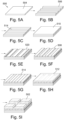
- Fig. 5A to 5I illustrate the steps of a particular method 500 of fabricating a sensor according to an embodiment of the invention.
- a base layer 504 is spin-coated, deposited, cast, or spray-coated into a thin membrane forming a bottom polymer encapsulation layer.
- the base layer 504 is made of an insulating polymer with desired elastic properties, such as PDMS or Parylene-C which may also form part of the binder material of the active layer. If spin-coating, this may be done on a silanized silicon wafer, so that the polymer does not get stuck and the device can be peeled off after production.
- Fig. 5A to 5I illustrate the steps of a particular method 500 of fabricating a sensor according to an embodiment of the invention.
- a base layer 504 is spin-coated, deposited, cast, or spray-coated into a thin membrane forming a bottom polymer encapsulation layer.
- the base layer 504 is made of an insulating polymer with desired
- a first electrode layer 506 is screen-printed, cast, sputter-coated, or spin-coated (e.g. using a photolithographic pattern) into a matrix array of bottom column electrodes.
- the first electrode layer 506 can be composed of conductive adhesives, such as carbon-impregnated elastomers, intrinsically conductive polymers, such as poly(3,4-ethylenedioxythiophene) polystyrene sulfonate (PEDOT:PSS) or a metal, such as gold or silver.
- Fig. 5C shows an optional step of adding an insulation layer 514 between each column electrode in the first electrode layer 506 for additional rigidity or robustness, using screen-printing or photolithographic patterning.
- the insulation layer 514 may be of the same material as the base layer 504.
- Fig. 5D shows the screen printing, casting, spin-coating, spray-coating or attachment of a thin active layer 510, for example, of a quantum tunnelling material such as those described above.
- the thickness of the active layer 510 may determine the sensitivity of the sensor and can vary from tens of microns to millimetres.
- the type of metal as well as the binding matrix material can vary according to the desired application and the composition of the material may be in the form of a liquid or solid.
- the active layer 510 could include gold nanoparticles and PDMS, or alternatively could include magnetite and water based polymeric ink. It may be a known material or a custom formulated material.
- Fig. 5E shows the screen-printing, casting, sputter-coating, or spin-coating (e.g. using a photolithographic pattern) to create a thin layer ( ⁇ 10-100um thick) of binder material to form spacers 520 only in areas between where electrodes are to be deposited, such that the electrode edges sit on top of the spacer edges. These spacers form a small air gap between the electrodes. Standard microfabrication or chemistry techniques such as pattering a layer which is partially dissolvable using e.g. photo-curable polymers may be utilised to create the air gap.
- Fig. 5F shows the screen-printing, casting, sputter-coating, spin-coating or attachment (e.g.
- the second electrode layer 508 can be composed of conductive adhesives, such as carbon-impregnated elastomers, intrinsically conductive polymers, such as PEDOT:PSS or a metal, such as gold or silver.
- a support layer is provided between the spacers 520 on which the top electrodes are formed.
- Fig. 5G shows an optional step of adding an insulation layer 514 between the top electrodes in the second electrode layer 508 for additional rigidity or robustness, using a screen-printing or photolithographic patterning technique.
- the insulation layer 514 may be of the same material as the base layer 504.
- a top layer 512 is spin-coated, deposited, cast, or spray-coated into a thin membrane to form a top polymer encapsulation layer.
- the top layer 512 may be made of an insulating polymer with the desired elastic properties, such as PDMS or Parylene-C and ideally may be formed of the same material as the binder material of the active layer 510.
- four three-dimensional surface bumps 502 are added into the top layer 512 by casting a polymer layer to form bumps 502 over every set of four overlapping electrodes or sensels.
- the bumps 502 may have a different elasticity and rigidity to the rest of the sensor (e.g. the bumps 502 may be more rigid than the sensor body).
- the three-dimensional shape of each bump 502 may be a cube, cone, or mesa/hemisphere, for example, and its corners should overlap to some extent with the four underlying electrodes. This gives each group of 4 electrodes (i.e. sensels) in the array the ability to become a single three-dimensional or tri-axial force sensing tactile element (tactel).
- an optional oxygen plasma layer, thiol layer or other chemical adhesive layer may be added to increase robustness of the sensor. If the base layer 502 has been spin-coated, then a further step may be required to detach the entire assembly from a wafer by peeling it off.
- the binder material for the above method is a stretchable elastomer, then it is possible to also make the entire sensor array stretchable, further increasing its potential applications.
- the substrate or base layer 504 used to create the sensor depends somewhat on the application.
- Traditional flexible electronics substrates that are complaint in only one axis such as PET (Polyethylene Terepthalate) varying in thickness from 25-125 microns and PEN (Polyethylene Naphtalate) varying in thickness from 10-100 micron (usually 25 micron) can be employed. These materials may be required when a high resolution is required, or in the case that the device needs to be resistant to a harsh external environment such as underwater.
- substrates compliant in more than one axis such as TPU (Thermoplastic Polyurethane) or silicone can be used. Or TPU coated silicone in order to reduce shrinkage induced in silicone during thermal curing of nanocomposite inks after deposition.
- a first layer of conductive ink may be printed, which functions as the conductive tracks for the first electrode layer 506 and is highly conductive.
- a stencil film or mask or screen printing mesh with appropriate openings cut out or washed away with solvent may be used, through which the ink can be spread onto the substrate using a squeegee as is common in screen printing or roll-to-roll printing.
- this electrode layer is made of a nanocomposite material and may be either flexible of stretchable. Stretchable inks work with substrates that may allow a percentage of stretch, such as TPU or silicone.
- Such inks contain conductive particles with one dimension often in the order of nanometers and an overall size often in the order of microns, and which are embedded into a polymer matrix usually mixed with solvent chemicals and surfactants that ensure an even dispersion between the particles in the ink.
- the particles typically consist of silver or carbon, but can equally be composed of gold, graphene, copper, tungsten, zinc, etc.
- the thickness of the deposited ink may be of the order of 10-50 microns (sometimes 100) in screen printing, but can also be less if inkjet printing it used.
- the width of some electrodes can be as low as 20 micron up to 1 millimeter.
- the electrode ink After the electrode ink is deposited, it must be cured, usually at a temperature between 80-120 0 C. During the curing process, part of the solvent evaporates while curing the polymer composite material.
- composition of tracks which may be required to connect the sensor to readout electronics and the electrodes themselves may either be the same composition, or made from a different composition.
- a coating with an ink with a different composition may be printed for the electrodes, on top of conductive tracks that extend to a region underneath each electrode.
- One or more layers of sensitive (potentially anisotropic i.e. being only sensitive to the normal direction, by means of the material thickness or its intrinsic properties) active layers is provided in each sensor.
- spacers consisting of a dielectric polymer may be printed or deposited onto the sensor using droplet dispensing methods. These spacers, which may be ⁇ 10-50 microns in height, and 1-200 microns in diameter or width, act to keep the grid layers of the sensor separated from each other until a specific force is applied. They also act to redistributed the force and prevent creasing or wrinkling of the sensor skin when bent, which in turn could create local pressure points or 'bubbles' that could cause a pressure reading on the sensor.
- stiffeners may be added to the ends of the connected electrode traces or tracks in the case of a highly compliant and stretchable material, or one that is extremely thin such as 25 micron or less, so that normal solder tabs or cables can be crimped to them, and the sensor electronics can be connected to a rigid electronic processing circuitry.
- Fig. 6A to 6I illustrate the steps of a method 600 of fabricating another sensor according to a further embodiment of the invention.
- the sensor is shown in both a three-dimensional and two-dimensional view.
- an appropriate substrate material 604 e.g. PEN, PET, TPU, PDMS, TPU coated Silicone, Latex, etc.
- the substrate 604 will form both a base layer and a top layer of the sensor as will be described in more detail below.
- the substrate 604 is PET which is 36 microns in thickness.
- Fig. 6B shows a step of printing (e.g.
- the electrodes are formed from an ink typically containing silver or low resistance carbon.
- the electrodes are made from CI-1036 stretchable silver-based conductive ink with low sheet resistivity of ⁇ 0.010 ⁇ /square at 25.4 microns thickness.
- the electrodes are screen printed at an emulsion thickness and hence have a thickness before curing of 14 to 25 microns.
- Each electrode has a width of 2mm and three electrodes are provided in each of the first and second electrodes layers 606, 608 so as to form a sensor which will be 1cm wide by 1cm long when assembled.
- a gap of 2mm is provided between the first electrode layer 606 and the second electrode layer 608 on the substrate 604 to allow each layer to be easily separated as will be described below.
- Fig. 6C shows an optional step of screen printing a carbon layer 607, 609 on each of the electrodes in the first and second electrode layers 606, 608.
- Fig. 6D shows a step of depositing (e.g. screen printing, inkjet printing, electro-spinning) an active layer 610 on each of the electrodes in the first and second electrode layer 606, 608.
- the active layer may comprise a piezoresistive and/or quantum tunnelling and/or piezoelectric material layer and can be deposited as a single layer or multiple layers on top of one another so as to control the layer thickness.
- the active layer may comprise a continuous sheet or discrete portions, for example, in the form of lines, squares, dots or other shapes.
- the active layer is formed of Quantum Technology SuperSensors (QTSS ® ) C75 piezoresistive ink printed on top of the electrode columns and rows on only the grid regions and with a similar thickness as the previous layers.
- QTSS ® Quantum Technology SuperSensors
- a spacer layer 620 is deposited using dielectric, insulating or conductive material.
- the spacer layer 620 may be deposited, for example, by screen printing, inkjet printing or using droplet dispenser. In this embodiment, the spacer layer 620 is formed on only one side of the substrate 604 in the gaps between the electrodes forming the second set of electrodes 608. In this example, the spacer layer 620 comprises an array of cylindrical posts, each having a diameter of 50 microns and a height of 100 microns, and being provided at a spacing of 1mm across the substrate 604.
- the material used for the spacer layer 620 in this example is a dielectric such as EMS DI-7548 which is stretchable as well as flexible.
- the spacer layer 620 can be printed on one side of the sensor in a single thick layer, multiple layers on top of one another, or both sides of the sensor if the layers are thin (although this requires precision alignment).
- the substrate 604 is cut, for example, with scissors, a laser, a knife plotter or scalpel to separate the first electrode layer 606 and the second electrode layer 608 into two parts. The two parts are then folded inwardly such that the second electrode layer 608 is stacked above the first electrode layer 606 to form a conductive matrix grid as shown in Fig. 6G .
- the substrate 604 attached to the second electrode layer 608 forms the top layer of the sensor.
- the posts of the spacer layer 620 extend between the substrate 604 forming the base layer and the substrate 604 forming the top layer such that there is an air gap 622 between the active layer 610 portions provided on the first electrode layer 606 and the second electrode layer 608.
- the spacer layer 620 serves to distribute force when the sensor is bent, and in this case also serves to maintain the air gap between the active layers 610, making sure an open circuit is present until a given offset force is applied.
- the sides of the sensor may be bonded with an adhesive paste (e.g. silicone PDMS) applied along the edges of the device and around the sensing layers region so as to seal it from the outside environment and laminate for sides of the sensor to each other in a durable manner.
- a vapour deposit of APTES (3-aminopropyl triethoxysilane) linker may be applied onto the top layer for 1h.
- the sensor may be fully coated with a compliant polymer such as latex at this stage. For extremely thin sensors, a dip-coating technique may be used.
- bumps 602 are then applied to the top surface of the sensor for translating fore into torque.
- the bumps In order to sense both the direction as well as the magnitude of the force, the bumps should be placed in the centre of each set of 4 orthogonally arranged electrodes (sensels), which converts any force applied into a torque when pressed. The torque will then compress some of the sensels more than others, and this can be read-out through an attached electronic circuit.
- the bumps can be made by printing multiple dielectric layers using various printing techniques (including 3D printing or silicon etching), or by casting the bumps in a mould (in this case the sensor needs to be placed upside down on the mould while the polymer to be used is in liquid state or partially cured state, then the entire assembly must be cured.
- a master mould is made from PLA for the four cubic bumps 602 which are 2mm in height and 6mm in length and width.
- Liquid PDMS or silicone/latex/TPU/Rubber
- the PDMS is treated with UV-Ozone or oxygen plasma to further increased adhesion before it is bonded to the PET top layer of the substrate 604.
- the assembly may be left to sit overnight to enable strong bonds to form between the PDMS bumps and the PET.
- the bumps 602 may be rigid or compliant themselves, as long as they allow the device to flex at the given thickness. Thinner bumps 602 as well as those made from highly compliant materials will distort measurements less upon bending and thus give better anisotropic selectivity to normal forces while the device is in a bent state.
- a final optional step may comprise laminating or insulating a top of the sensor or edges of the sensor or the entire sensor structure to make a cover layer 624 which is impermeable to outside elements.
- Lamination can be done with e.g. a Parylene coating which is completely conformal (more specifically Parylene-C of 1 nanometer to 1 micron thickness), and insulation may be achieved with a silicone, rubber, polyurethane, or other polymer blend.
- any suitable printer can be employed for any of the layers in the sensor.
- a suitable screen printer is Horizon Dek i3 TM .
- the readout of the sensor can be done using a known zero potential method. This minimizes crosstalk between adjacent sensors within large arrays.
- a large interference current can be generated when the resistance of one sensing element approaches that of others around it.
- the sensing elements begin at a high resistance and reduce in resistance as pressure is applied. This means that in the sensors described, low pressures produce a higher interference as the material has a high resistance at rest. Moe details on the operation of these sensors are provided below in relation to Fig.'s 12A to C.
- Fig. 7A to 7G illustrate the steps of a method of fabricating a sensor according to a yet further embodiment of the invention.
- This sensor can be considered a 4-wire single point sensor which operates differently to the other sensors described above.
- this sensor differs in that it measures the 'centre of mass' of the pressure being applied in a resistive area that is between the 4 wires in the electrode grid.
- the bump for this sensor functions in a similar way to a joystick in that the position of the centre of mass can give us the direction of force.
- Fig. 7A an appropriate substrate 704 material is selected along with its thickness.
- the substrate 704 is formed of PET at 36 microns thickness.
- FIG. 7B shows the screen printing of both the first and second electrode layers 706, 708 on the same substrate 704, with the electrodes in each layer oriented perpendicularly to each other.
- the electrodes are made of EMS CI-1036 TM stretchable silver-based conductive ink with a low sheet resistivity of ⁇ 0.010 ⁇ /square at 25.4 microns thickness.
- the electrodes are screen printed at an emulsion thickness such that the ink thickness before curing is 14 to 25 microns.
- the electrodes are 2mm wide and only two electrodes are provided along the edges of each of the first and second electrode layers 706, 708 to form a 1cm by 1cm footprint sensor.
- Fig. 7C shows the screen printing of a first high resistance carbon layer 707 deposited on top of and extending between the two electrodes in the first electrode layer 706 and a second high resistance carbon layer 709 deposited on top of and extending between the two electrodes in the second electrode layer 709.
- both high resistance carbon layers are blended from two Henkel TM inks called ECI 7004 HR and NCI 7002 Ink (80/20 % by weight blend) to give a sheet resistivity of ⁇ 10,100 ⁇ /square/mil at 10 microns thickness after curing.
- the deposition is performed through a mesh with ⁇ 20-40 microns emulsion thickness.
- the high resistance carbon layers may be formed using EMS TM CI-2050 LR (1,500 - 2,500 ⁇ /square/mil at 25.4 microns) and/or HR (>10M ⁇ /square/mil at 25.4 microns).
- the first and second high resistance carbon layers 707, 709 may be different.
- the high resistance carbon layers 707, 709 are of a much higher resistance than the sum of the lead resistance within the device and the contact resistance for interfacing with the outside world.
- the reason for this is that, when a voltage is applied across the top electrode layer 708 or the bottom electrode layer 706 of the device, it is desirable that most of the voltage drop occurs within the resistive carbon region. This ensures that the position of the centre of pressure of the torque applied to the bump layer may be measured: when a pressure is applied to the device, both active layers 710 contact each other around a given point.
- Fig. 7D shows the screen-printing, inkjet printing or electro-spinning of an active layer 710 on each of the first high resistance carbon layer 707 and the second high resistance carbon layer 709.
- the active layer 710 is formed of Quantum Technology SuperSensors (QTSS ® ) C75 piezoresistive water-based ink.
- QTSS ® Quantum Technology SuperSensors
- a spacer layer 720 comprising a square array of short cylindrical spacer dots is provided on the active layer 710 on one side (the first side) of the substrate. Each spacer dot is 200 microns in height and is spaced 2mm apart from its neighbour.
- the spacer layer 720 is printed using Stratasys' Tango TM (i.e. TangoPlus TM , FLX930) material, which is a PolyJet TM printable material that simulates rubbery thermoplastic elastomers.
- the typical properties of the material are a shore hardness of 26-28 and an elongation at break at 170-220%.
- the spacers can therefore withstand the difference between tensile and compressive stress at the top and bottom of the device while curved, even if applied while the device itself is flat.
- the substrate 704 is then cut, for example, with scissors, a laser, a knife plotter or scalpel to separate the first electrode layer 706 and the second electrode layer 708 into two parts. The two parts are then folded inwardly such that the second electrode layer 708 is stacked above the first electrode layer 706 to form a conductive matrix grid as shown in Fig. 7E . In this configuration the substrate 704 attached to the second electrode layer 708 forms the top layer of the sensor.
- the posts of the spacer layer 720 extend between the active layer 710 on the first electrode layer 706 and the active layer 710 on the second electrode layer 708 such that there is an air gap in the middle of the active layer 710 as shown in Fig. 7F .
- a silicone PDMS adhesive applied around the edges of the device.
- a vapour deposit of APTES (3-aminopropyl triethoxysilane) linker is then applied onto the top surface of the device for 1h in order to facilitate PDMS adhesion described below.
- a bump 702 is provided in the middle of the sensor, spaced from the electrode grid.
- the bump 702 may be cast or printed and many polymers can be used for this, e.g. more compliant PDMS, or less compliant SU8.
- the bump 702 can have various shapes, sizes, and heights depending on the desired application.
- a master mould is made from PLA for the cuboid bump 702 which is 2mm in height and has a length and width of 6mm.
- Liquid PDMS is cast into the mould (10:1 weight ratio of elastomer to curing agent) and cured in an oven for 1h at 80 degrees Celsius. After this, the PDMS is treated with UV-Ozone or oxygen plasma to further increased adhesion before it is bonded to the top layer of the substrate 704. The assembly is left to sit overnight to enable strong bonds to form between the PDMS bumps and the substrate 704.
- the readout consists of three separate readings for each bump 702. One reading is required for the X-location and another for the Y-location as explained below. Each time, a voltage (and current) is applied across the electrodes of one plane (i.e. the first or second electrode layer 706, 708) and one of the electrodes on the opposite plane (i.e. the other of the first or second electrode layer 706, 708) is used to readout a voltage.
- This forms a potential divider circuit where the voltage being read corresponds to the (x or y) position at which both planes touch, which is where the force is being applied. It is important that the high resistance carbon layers are much higher in resistance that the leads and contact resistances connecting the device to the outside world, so that they are essentially negligible. Otherwise, the location readings become restricted as some significant voltage drop will occur in the leads.
- a current must be passed from one plane to the other, with the active layer 710 (i.e. piezoresistive material) in between.
- the active layer 710 i.e. piezoresistive material
- This can be done by applying a potential difference between one electrode on the top plane (i.e. the second electrode layer 708) and another on the bottom plane (i.e. the first electrode layer 706).
- the pressure applied affects the active layer's resistance which in turn changes the current through the device.
- the bump 702 on top of the sensor experiences a force
- its shear component causes a torque on the bump 702 which focuses the centre of the pressure into a particular region of the device. Measuring the location and magnitude of this allows measurement of the average direction and magnitude of the force.
- Fig.'s 8A to 11C show various example spacer arrangements for use in embodiments of the invention. For illustrative purposes only a portion of the sensor is shown in each case.
- Fig.'s 8A and 8B show plan views of a portion of a sensor including different cylindrical spacer arrangements according to embodiments of the invention.
- a substrate 804 is provided with three horizontal electrodes in a first electrode layer 806 and three orthogonal electrodes in a second electrode layer 808.
- An active material 810 is provided between the electrodes in the first electrode layer 806 and the second electrode layer 808.
- the spacers are formed of cylindrical posts, pillars or dots.
- the spacers 820a are printed on both sides of the substrate 804, and are arranged to extend from or through each electrode layer to the substrate 804 between electrode matrix overlaps.
- the spacers 820b are printed on only one side of the substrate 804, and are arranged to extend between the lower and upper portions of the substrate 804 between electrode matrix overlaps.
- the spacers in Fig.'s 8A and 8B may be formed of polymers such as dielectric polymers, polysiloxanes, rubbers or silicones or amorphous crystalline substances such as glass.
- the spacers may be shaped to be cylindrical, cone or cone section, pyramid or pyramid section, cuboid, hemispherical or hemispherical section, half-cylinder, tetrahedron or tetrahedron section, hexahedron, triangular prism, polyhedron, other shapes.
- the spacers may be graded such that they change in height, shape, dimensions or spacing across the sensor.
- the spacers may be cone shaped with a width of 50 microns, a height of 25 microns and a spacing of 1mm.
- Fig.'s 9A and 9B show plan views of a portion of a sensor including different diamond spacer arrangements according to embodiments of the invention.
- a substrate 904 is provided with three horizontal electrodes in a first electrode layer 906 and three orthogonal electrodes in a second electrode layer 908.
- An active material 910 is provided between the electrodes in the first electrode layer 906 and the second electrode layer 908.
- the spacers are formed of a diamond or square mesh.
- the spacers 920a are printed on only one side of the substrate 904, and are arranged to extend from or through each electrode layer between electrode matrix overlaps.
- the spacers 920b are printed on both sides of the substrate 904, and are arranged to extend on and/or between the lower and upper portions of the substrate 904 on and/or between electrode matrix overlaps.
- the spacers in Fig.'s 9A and 9B may be formed of a woven fabric mesh or flexible/rubbery polymer mesh which is, for example, 3D printed using any of various soft polymers.
- Fig.'s 10A and 10B show plan views of a portion of a sensor including different square spacer arrangements according to embodiments of the invention.
- a substrate 1004 is provided with three horizontal electrodes in a first electrode layer 1006 and three orthogonal electrodes in a second electrode layer 1008.
- An active material 1010 is provided between the electrodes in the first electrode layer 1006 and the second electrode layer 1008.
- the spacers are formed of a hollow square post.
- the spacers 1020a are printed on only one side of the substrate 1004, and are arranged to extend around a large sensor area, for example, encompassing nine electrode overlaps with a single square.
- the spacers 1020b are printed on only one side of the substrate 1004, and are arranged to extend around a small sensor area, for example, between each electrode matrix overlap.
- the spacers in Fig.'s 10A and 10B may be formed of similar materials to those described above for the cylindrical or diamond spacers.
- Fig.'s 11A, 11B and 11C show plan views of a portion of a sensor including different hexagonal spacer arrangements according to embodiments of the invention.
- a substrate 1104 is provided with three horizontal electrodes in a first electrode layer 1106 and three orthogonal electrodes in a second electrode layer 1108.
- An active material 1110 is provided between the electrodes in the first electrode layer 1106 and the second electrode layer 1108.
- the spacers are formed of a hollow hexagonal (i.e. honeycomb) mesh of a different size.
- the spacers 1120a are printed on only one side of the substrate 1104, and are arranged to extend between electrode matrix overlaps.
- the spacers 1120b are printed on only one side of the substrate 1104, and are arranged to extend around a small sensor area, on and/or between each electrode matrix overlap.
- the spacers 1120c are printed on only one side of the substrate 1104, and are arranged to extend between electrode matrix overlaps and to bound said electrode matrix overlaps.
- the spacers in Fig.'s 11A, 11B and 11C may be formed of extruded or printed meshes. These may be in the shape of honeycomb, triangular, quadrilateral, diamond, diamond with ferrule, square or plain. A variety of different weaves can be chosen depending on the application and must ensure enough of the sensors active layers can contact one-another.
- the woven mesh has the same purpose as other spacer layers. A plain Dutch weave, twill weave, plain weave, twill Dutch, lock crimp, inter-crimp, twill Dutch double or stranded weave may be employed amongst others.
- the mesh may be made of non-conductive textile thread or electrically conductive thread (e.g. silver or titanium) could be used for enhancing sensitivity while distributing pressure within the sensor.
- a quantum tunnelling active layer material is advantageous as it starts at a very high resistance ( ⁇ 10 9 ⁇ ). Contacts to this material can be made up of multiple different materials, however the electrodes must be compliant and slightly elastic so that the material can be used to wrap around objects. One way to do this is to make stretchable silver electrodes, or alternately use conductive adhesives, even if they vary slightly according to pressure.
- a simple device where not only is the entire device itself compliant, but every cluster of 4 sensels in a grid can be transformed into a 3D force sensing 'tactel' (tactile pixel) by including 'bumps' or shapes which act as a force transmission structure for the top layer of the device.
- the device proposed is made for mass-production using printing such as roll-to-roll printing, screen printing or similar microfabrication techniques.
- the main working mechanism of the sensors described above is the following: changes in the resistance of each of the 4 sensels, as well as their normal distribution, are used to estimate tri-directional forces on the sensor.
- Each bump acts as a force transmission structure.
- a stress is generated by deforming the 'bump'.
- the normal component of the force compresses each sensel underneath it equally (resulting in symmetrical resistive changes), however the shear component generates a torque in the active layer which compresses some sensels more than others (resulting in an asymmetrical resistance change).
- Tuning the sensitivity of this can be done both by varying the thickness and binding material of the active layer as well as the height and rigidity of the 'bump' and the underlying substrate materials.
- Individual grid lines can be made as small as 10um, and the spacing between then as small as necessary provided tunnelling is not established between the layers which would create cross-talk and short-circuits.
- each column and row electrode In order to read-out the signal, each column and row electrode must be connected to appropriate electrical readout circuitry. When reading out the signal, since each electrode is spatially separated from one another, resistive cross-talk noise is significantly reduced. However, to achieve a further reduction in cross-talk or an increase in the signal-to-noise ratio (SNR) of each sensel, one of the following methods may be adopted: i) Pubrick's voltage mirror method, where drive lines that are not under consideration at a measuring point are set at a potential equal to the output voltage, or ii) the simpler zero potential method where the voltage of the scanning electrodes is set to zero. These form an equal potential zone that eliminates the effect of cross-talk. There are multiple ways to configure the above circuits in practice.
- the force ranges that can be measured with such a sensor range from 0.01N up to a theoretically infinite quantity, depending on the formulation of the active layer, its binder, and the overall thickness of the sensor.
- the layers have a preferred thickness, however for the entire device to be compliant it is expected that they be no more than 1mm thick and no less than 10nm thin.
- the bumps on the surface may comprise different shapes to those listed, however the constraint of having 1 bump for every 4 sensels applies in most cases.
- Fig. 12A shows a top perspective view of a single tactile element (tactel) 1200 of a sensor according to an embodiment of the invention.
- This tactel has a dome-shaped bump 1202 provided over 4 sensels C1, C2, C3 and C4 which represent the pixels to be read.
- Table 1 below shows the change in electrical resistance experienced by each of the 4 sensels when subjected to different forces. Thus it can be determined how the electrical readout for such a sensor can be translated into a measurement of the position, size and direction of an applied force.
- Table 1 Sensel change in response to force direction
- Direction of force Change of electrical resistance C1 C2 C3 C4 Shear force +X + + - X + + + +Y + + -Y + + Normal force Z + + + + + + + + +
- Fig. 12B shows a side perspective view of the tactile element 1200 of Fig. 12A before and after an oblique force is applied to the bump 1202, along with a corresponding force v time graph. This illustrates the difference in force experienced in the x, y and z axes when the oblique force is applied.
- Fig. 12C shows a side view of the tactile element 1200 of Fig. 12B when the oblique force is applied to the bump 1202.
- the sensel C3 experiences a small deformation while the sensel C4 experiences a large deformation on application of the force. This is translated into a weaker change in C3 than in C4 which helps to pinpoint the direction of the applied force.
- toys or dolls with real-time performance/feedback and/or adaptive devices pillows that sense movement, hospital beds that monitor bed sores, blood pressure monitoring and detection (e.g. for coronary heart disease (CVD) diagnosis by monitoring blood pressure and flow through e.g. a garment or wearable), muscular force/exertion, fatigue monitoring and detection, tidal or wind turbine monitoring of flow characteristics around a blade to increase lifespan or energy generation capacity, all areas where autonomous robots may be envisaged and require high levels of dexterity and tactile information (e.g.
- CVD coronary heart disease
- aeroplane wings monitoring loads/forces which can help in weight and cost reduction as well as better wing design
- monitoring of forces in construction work environments horse saddle pressure monitoring, muscular force mapping/monitoring, tissue hardness/density monitoring (e.g. diagnosis of breast cancer/ how close a woman is to giving birth), prosthetics (e.g. for amputees but also for tremor compensation for certain diseases such as Parkinson's, ALS, etc.), amongst others.
- piezoresistive and piezoelectric layers could be stacked before applying a bump layer, in order to better imitate high and low frequency mechanoreceptors in the skin.
- the device could be used upside-down (i.e. with the bumps abutting a user's skin and a force being applied through the base layer), which may be especially beneficial if aerodynamic or hydrodynamic properties are to be maintained on the surface of the device.
Landscapes
- Chemical & Material Sciences (AREA)
- Analytical Chemistry (AREA)
- Physics & Mathematics (AREA)
- General Physics & Mathematics (AREA)
- Force Measurement Appropriate To Specific Purposes (AREA)
- Pressure Sensors (AREA)
Claims (15)
- Nachgiebiger dreiachsiger Kraftsensor (100), Folgendes umfassend:eine erste Elektrodenschicht (106) mit einer Anordnung von Säulenelektroden (106a) in einer ersten Ausrichtung;eine zweite Elektrodenschicht (108) mit einer Anordnung von Säulenelektroden (108a) in einer zweiten Ausrichtung, die orthogonal zur ersten Ausrichtung ist;eine kraftabhängige aktive Schicht (110), die konfiguriert ist, um mindestens eine Eigenschaft zu ändern, wenn sie einer Kraft ausgesetzt wird, und die zwischen der ersten Elektrodenschicht (106) und der zweiten Elektrodenschicht (104) bereitgestellt ist;mindestens eine dreidimensionale Erhebung (102), die angeordnet ist, um eine extern angewendete Kraft durch die aktive Schicht (110) zu übertragen;wobei mindestens ein Abstandhalter (620) bereitgestellt ist, der angeordnet ist, um eine Trennung zwischen zwei oder mehr Schichten in dem Sensor (100) aufrechtzuerhalten, bis eine externe Kraft angewendet wird; undwobei die mindestens eine dreidimensionale Erhebung (102) eine Grundfläche aufweist, die entweder:sich mindestens teilweise über mindestens zwei Säulenelektroden (106a) in der ersten Elektrodenschicht (106) und mindestens teilweise über mindestens zwei Säulenelektroden (108a) in der zweiten Elektrodenschicht (108) erstreckt, sodass auf die Erhebung (102) ausgeübte Kräfte durch die aktive Schicht (110) in mindestens vier diskreten Bereichen übertragbar sind; oderinnerhalb eines Raums zwischen zwei Säulenelektroden (106a) in der ersten Elektrodenschicht (106) und zwischen zwei Säulenelektroden (108a) in der zweiten Elektrodenschicht (108) enthalten ist.
- Sensor (100) nach Anspruch 1, wobei die aktive Schicht (110) mindestens eines der folgenden Materialien umfasst: ein Quanten-Tunneleffekt-Material, ein piezoresistives Material oder ein piezoelektrisches Material.
- Sensor (100) nach Anspruch 1 oder 2, wobei die mindestens eine Eigenschaft Folgendes ist: Quanten-Tunneleffekt; Leitfähigkeit; Widerstand oder elektrische Ladung.
- Sensor (100) nach einem der vorhergehenden Ansprüche, wobei die aktive Schicht (110) eine erste aktive Schicht und eine zweite aktive Schicht mit einem Spalt zwischen diesen umfasst.
- Sensor (100) nach einem der vorhergehenden Ansprüche, ferner umfassend eine oder mehrere der folgenden Komponenten: eine Basisschicht (104) unter der ersten Elektrodenschicht (106); eine obere Schicht (112) über der zweiten Elektrodenschicht (108); eine erste Kohlenstoffschicht (607) zwischen der ersten Elektrodenschicht (106) und der aktiven Schicht (110); eine zweite Kohlenstoffschicht (609) zwischen der zweiten Elektrodenschicht (108) und der aktiven Schicht (110); und eine Deckschicht (624) über der mindestens einen dreidimensionalen Erhebung (102); wahlweise, wobei die erste und/oder zweite Kohlenstoffschicht (607; 609) über mehrere Säulenelektroden (106a; 108a) in der ersten und/oder zweiten Elektrodenschicht (106; 108) durchgehend ist.
- Sensor (100) nach einem der vorhergehenden Ansprüche, wobei der mindestens eine Abstandhalter (620) innerhalb der aktiven Schicht (110); zwischen der Basisschicht (104) und der oberen Schicht (112); oder auf oder durch die erste oder zweite Elektrodenschicht (106; 108) bereitgestellt ist; und/oder wobei der mindestens eine Abstandhalter (620) in der Form eines Punktes, einer Säule, eines Pfostens, eines Zylinders, eines Rohrs, einer Pyramide oder eines Netzes vorliegt; und/oderwobei der mindestens eine Abstandhalter (620) einen massiven oder hohlen Querschnitt in der Form eines Kreises, Quadrats, Rechtecks, einer Raute, eines Fünfecks, Sechsecks oder eines Wabenmusters aufweist.
- Sensor (100) nach einem der vorhergehenden Ansprüche, umfassend eine Anordnung der Abstandshalter (620); wahlweise, wobei die Abstandshalter (620) in der Anordnung eine Vielzahl unterschiedlicher Abmessungen aufweisen.
- Sensor (100) nach einem der vorhergehenden Ansprüche, wobei die aktive Schicht (110) eine kontinuierliche Schicht über mehrere Säulenelektroden (106a; 108a) in der ersten und/oder zweiten Elektrodenschicht (106; 108) bildet; oder wobei die aktive Schicht (110) eine diskontinuierliche Schicht über die Säulenelektroden (106a; 108a) in der ersten und/oder zweiten Elektrodenschicht (106; 108) bildet.
- Sensor (100) nach einem der vorhergehenden Ansprüche, wobei ein Isolator (114; 116) zwischen angrenzenden Elektroden (106a; 108a) in der ersten und/oder zweiten Elektrodenschicht (106; 108) bereitgestellt ist.
- Sensor (100) nach einem der vorhergehenden Ansprüche, wobei mindestens ein Abstandhalter (620) die Form eines Bindemittels annimmt, das zwischen der aktiven Schicht (110) und der ersten und/oder zweiten Elektrodenschicht (106; 108) bereitgestellt ist, wobei das Bindemittel in Spalten zwischen angrenzenden Säulenelektroden (106a; 108a) bereitgestellt ist und sich zwischen der aktiven Schicht (110) und jeweiligen Rändern der angrenzenden Säulenelektroden (106a; 108a) erstreckt.
- Sensor (100) nach einem der vorhergehenden Ansprüche, wobei eine Haftschicht zwischen einer oder mehreren angrenzenden Schichten bereitgestellt ist.
- Sensor (100) nach einem der vorhergehenden Ansprüche, wobei die mindestens eine dreidimensionale Erhebung (102) ein Polymer umfasst, das eine Elastizität aufweist, die sich von einem Rest des Sensors (100) unterscheidet; und/oder wobei die mindestens eine dreidimensionale Erhebung (102) in der Form einer Plattform, einer Kuppel, einer Halbkugel, einer halbkugelförmigen Sektion, eines Kegels, einer kegelartigen Sektion, eines Quaders, eines Zylinders, eines Halbzylinders, einer Pyramide, einer pyramidenartigen Sektion, eines Tetraeders, einer tetraederförmigen Sektion, eines Hexaeders, eines dreieckigen Prismas oder eines Polyeders vorliegt; und/oder wobei die mindestens eine dreidimensionale Erhebung (102) eine Höhe aufweist, die mindestens das Doppelte einer Höhe eines Rests des Sensors (100) beträgt.
- Sensor (100) nach einem der vorhergehenden Ansprüche, umfassend eine Anordnung der dreidimensionalen Erhebungen (102).
- Verfahren zum Herstellen eines Sensors (100) nach einem der vorhergehenden Ansprüche, Folgendes umfassend:Bereitstellen einer ersten Elektrodenschicht (106) mit einer Anordnung von Säulenelektroden (106a) in einer ersten Ausrichtung;Bereitstellen einer zweiten Elektrodenschicht (108) mit einer Anordnung von Säulenelektroden (108a) in einer zweiten Ausrichtung, die orthogonal zur ersten Ausrichtung ist;Bereitstellen einer kraftabhängigen aktiven Schicht (110), die konfiguriert ist, um mindestens eine Eigenschaft zu ändern, wenn sie einer Kraft ausgesetzt wird, und die zwischen der ersten Elektrodenschicht (106) und der zweiten Elektrodenschicht (108) bereitgestellt ist;Bereitstellen mindestens einer dreidimensionalen Erhebung (102), die angeordnet ist, um eine extern angewendete Kraft durch die aktive Schicht (110) zu übertragen;Bereitstellen mindestens eines Abstandhalters (620), der angeordnet ist, um eine Trennung zwischen zwei oder mehr Schichten in dem Sensor (100) aufrechtzuerhalten, bis eine externe Kraft angewendet wird; undwobei die mindestens eine dreidimensionale Erhebung (102) eine Grundfläche aufweist, die entweder:sich mindestens teilweise über mindestens zwei Säulenelektroden (106a) in der ersten Elektrodenschicht (106) und mindestens teilweise über mindestens zwei Säulenelektroden (108a) in der zweiten Elektrodenschicht (108) erstreckt, sodass auf die Erhebung (102) ausgeübte Kräfte durch die aktive Schicht (110) in mindestens vier diskreten Bereichen übertragbar sind; oderinnerhalb eines Raums zwischen zwei Säulenelektroden (106a) in der ersten Elektrodenschicht (106) und zwischen zwei Säulenelektroden (108a) in der zweiten Elektrodenschicht (108) enthalten ist.
- Verfahren nach Anspruch 14, wobei jede Schicht (106; 108), jede Erhebung (102) oder jeder Abstandhalter (620) durch eines von Folgenden bereitgestellt wird: Drucken, Siebdruck, Rolle-zu-Rolle-Druck, Tintenstrahldruck, 3D-Druck, Elektrospinnen, Ablagern, Tröpfchenabgabe, Gießen, Beschichten, Formen, Spinnen oder Weben; und/oder umfassend das Bilden mindestens der ersten Elektrodenschicht (106) und der zweiten Elektrodenschicht (108) auf einem einzelnen Substrat; das Trennen des Substrats in zwei Teile; und das Stapeln der beiden Teile gemeinsam; wahlweise umfassend das Bilden des mindestens einen Abstandshalters (620) auf mindestens einem Teil vor dem Trennen und/oder dem Stapeln.
Applications Claiming Priority (2)
| Application Number | Priority Date | Filing Date | Title |
|---|---|---|---|
| GBGB1910563.4A GB201910563D0 (en) | 2019-07-24 | 2019-07-24 | A compliant tri-axial force sensor and method of fabricating the same |
| PCT/EP2020/070636 WO2021013874A1 (en) | 2019-07-24 | 2020-07-22 | A compliant tri-axial force sensor and method of fabricating the same |
Publications (3)
| Publication Number | Publication Date |
|---|---|
| EP4004513A1 EP4004513A1 (de) | 2022-06-01 |
| EP4004513B1 true EP4004513B1 (de) | 2025-05-14 |
| EP4004513C0 EP4004513C0 (de) | 2025-05-14 |
Family
ID=67839729
Family Applications (1)
| Application Number | Title | Priority Date | Filing Date |
|---|---|---|---|
| EP20746593.1A Active EP4004513B1 (de) | 2019-07-24 | 2020-07-22 | Ein elastischer dreiachsiger kraftsensor und verfahren zur herstellung des gleichen |
Country Status (9)
| Country | Link |
|---|---|
| US (1) | US12216017B2 (de) |
| EP (1) | EP4004513B1 (de) |
| JP (1) | JP7602809B2 (de) |
| KR (1) | KR20220039781A (de) |
| CN (1) | CN114521232B (de) |
| ES (1) | ES3031739T3 (de) |
| GB (1) | GB201910563D0 (de) |
| PL (1) | PL4004513T3 (de) |
| WO (1) | WO2021013874A1 (de) |
Families Citing this family (29)
| Publication number | Priority date | Publication date | Assignee | Title |
|---|---|---|---|---|
| US20220175292A1 (en) * | 2017-03-01 | 2022-06-09 | CB Innovations, LLC | Screen Printed Electrodes For An Electrocardiogram Article |
| GB201910563D0 (en) | 2019-07-24 | 2019-09-04 | Hussein Zakareya Elmo | A compliant tri-axial force sensor and method of fabricating the same |
| CN111157151B (zh) * | 2020-03-04 | 2026-03-10 | 桂林智工科技有限责任公司 | 基于压电单元的三维力感知阵列传感器及压力解算方法 |
| US12546672B2 (en) * | 2020-03-16 | 2026-02-10 | New York University | Apparatus for determining shear forces in regard to a pressure imaging array, single point sensor for shear forces, and method |
| US11852546B2 (en) * | 2020-11-25 | 2023-12-26 | Nitto Bend Technologies, Inc. | Systems and methods for foldable multi-mode bend sensors |
| EP4019926A1 (de) * | 2020-12-22 | 2022-06-29 | Max-Planck-Gesellschaft zur Förderung der Wissenschaften e.V. | System und verfahren zur gleichzeitigen erfassung von kontaktkraft und seitlicher belastung |
| JP7560031B2 (ja) * | 2021-01-20 | 2024-10-02 | 本田技研工業株式会社 | 3軸力センサ |
| JP2022187868A (ja) * | 2021-06-08 | 2022-12-20 | 本田技研工業株式会社 | 力検出装置 |
| CN117501082A (zh) * | 2021-06-29 | 2024-02-02 | 新加坡国立大学 | 力传感器和包含力传感器的设备 |
| CN114181565A (zh) * | 2021-10-21 | 2022-03-15 | 嘉兴聚鑫隆科技有限公司 | 用于柔性传感器的压电基材及其制造工艺 |
| US20230160762A1 (en) * | 2021-11-25 | 2023-05-25 | National Taiwan University Of Science And Technology | Pressure Sensing Element with Porous Structure Based Flexible Base |
| WO2023183241A1 (en) * | 2022-03-20 | 2023-09-28 | Massachusetts Institute Of Technology | Resistive sensing arrays and methods of manufacturing the same |
| GB202208480D0 (en) * | 2022-06-09 | 2022-07-27 | Ucl Business Ltd | Force sensing |
| US11561138B1 (en) * | 2022-06-28 | 2023-01-24 | RET Equipment Inc. | Resistive pressure sensor with improved structure design |
| KR102879207B1 (ko) * | 2023-01-05 | 2025-10-30 | 동국대학교 산학협력단 | 다기능 인장센서 및 이의 제조방법 |
| CN116429313B (zh) * | 2023-02-20 | 2026-01-06 | 北京理工大学 | 一种用于测量固液两相流动力学信息的装置及方法 |
| GB2628117B (en) * | 2023-03-14 | 2026-04-01 | Infi Tex Ltd | Flexible pressure sensors, conductive transfers, and methods of manufacture for such |
| CN116698235B (zh) * | 2023-07-04 | 2026-04-07 | 杭州电子科技大学 | 一种双层锥形阵列柔性压力传感器制备方法及应用 |
| WO2025053793A1 (en) * | 2023-09-06 | 2025-03-13 | National University Of Singapore | Oral input device |
| DE102024100266A1 (de) * | 2024-01-05 | 2025-07-10 | Haake Technik Gmbh | Gefalteter Taktiler Sensor |
| US12613151B2 (en) | 2024-01-29 | 2026-04-28 | Nano And Advanced Materials Institute Limited | High sensitivity, wide range and any size printed pressure distribution monitoring ultrathin flexible mat system |
| CN119413322B (zh) * | 2024-09-18 | 2025-10-31 | 西安交通大学 | 嵌入式液态金属微结构电极、柔性压力传感器阵列及制备方法 |
| CN119512375A (zh) * | 2024-11-19 | 2025-02-25 | 北京理工大学 | 一种基于压阻式压力传感器的智能手套 |
| CN119533720A (zh) * | 2024-11-19 | 2025-02-28 | 北京理工大学 | 一种具备刚性触点的阵列式柔性压力传感器及其制备方法 |
| CN119665798B (zh) * | 2024-11-22 | 2026-01-30 | 武汉真友科技有限公司 | 一种柔性应变传感器及其制备方法 |
| CN119594841B (zh) * | 2024-12-04 | 2025-10-03 | 西安电子科技大学杭州研究院 | 一种基于定向pvdf纤维的可拉伸压电式传感器的制备方法 |
| CN119880233B (zh) * | 2025-01-17 | 2025-10-10 | 河北工业大学 | 一种平面型柔性三维力传感系统 |
| CN119563969B (zh) * | 2025-02-08 | 2025-04-25 | 悟通感控(北京)科技有限公司 | 足底多维压力感测装置和系统 |
| CN120820270B (zh) * | 2025-08-26 | 2026-03-03 | 中国科学技术大学 | 一种折纸结构电感式自解耦微型六维力传感器 |
Family Cites Families (34)
| Publication number | Priority date | Publication date | Assignee | Title |
|---|---|---|---|---|
| US4503705A (en) * | 1982-02-24 | 1985-03-12 | The Langer Biomechanics Group, Inc. | Flexible force sensor |
| CN1796955A (zh) * | 2004-12-28 | 2006-07-05 | 中国科学院合肥智能机械研究所 | 一种柔性触觉传感器 |
| JP4364146B2 (ja) | 2005-03-10 | 2009-11-11 | 株式会社東芝 | 触覚センサー |
| HUP0600892A2 (en) * | 2006-11-30 | 2008-06-30 | Pazmany Peter Katolikus Egyete | Elastic cover for tactile sensors and tactile sensing arrangement with elastic cover |
| US7509884B2 (en) * | 2007-02-01 | 2009-03-31 | Nitta Corporation | Sensor sheet |
| JP2008209384A (ja) | 2007-02-01 | 2008-09-11 | Nitta Ind Corp | センサシート |
| US8161826B1 (en) * | 2009-03-05 | 2012-04-24 | Stryker Corporation | Elastically stretchable fabric force sensor arrays and methods of making |
| TWI420086B (zh) * | 2008-10-15 | 2013-12-21 | Ind Tech Res Inst | 軟性電子壓力感測裝置及其製造方法 |
| TWI467601B (zh) * | 2009-08-31 | 2015-01-01 | Universal Cement Corp | 微形變壓阻材料及其製作方法 |
| US9112058B2 (en) * | 2010-09-10 | 2015-08-18 | The Board Of Trustees Of The Leland Stanford Junior University | Interface apparatus and methods |
| US8069735B1 (en) * | 2010-11-10 | 2011-12-06 | Artann Laboratories Inc. | Tactile sensor array for soft tissue elasticity imaging |
| JP2012173079A (ja) | 2011-02-21 | 2012-09-10 | Seiko Epson Corp | センサー素子、センサーデバイス、力検出装置およびロボット |
| US9271665B2 (en) * | 2011-05-20 | 2016-03-01 | The Regents Of The University Of California | Fabric-based pressure sensor arrays and methods for data analysis |
| KR101312550B1 (ko) * | 2011-10-31 | 2013-10-14 | 한국표준과학연구원 | 신축성 촉각센서를 구비한 유연 터치패널, 신축성 촉각센서 및 그 제조방법 |
| KR101312553B1 (ko) * | 2011-12-28 | 2013-10-14 | 한국표준과학연구원 | 촉각 센서의 곡면 부착구조 및 촉각 센서의 곡면 부착방법 |
| WO2014018318A1 (en) * | 2012-07-27 | 2014-01-30 | Tactonic Technologies, Llc | Method for mechanical sensing utilizing controlled current |
| JP6128581B2 (ja) * | 2012-10-26 | 2017-05-17 | 国立大学法人信州大学 | 柔軟接触型4軸荷重測定システム |
| KR101979680B1 (ko) * | 2012-12-05 | 2019-05-20 | 삼성전자주식회사 | 촉각센서 |
| TWI470197B (zh) * | 2012-12-20 | 2015-01-21 | Ind Tech Res Inst | 電容式剪力感測器及其製造方法 |
| KR101452302B1 (ko) * | 2013-07-29 | 2014-10-22 | 주식회사 하이딥 | 터치 센서 패널 |
| CN103954382B (zh) | 2014-05-14 | 2016-02-24 | 合肥工业大学 | 一种变介质式电容柔性三维力触觉传感器 |
| US20170350772A1 (en) * | 2014-12-23 | 2017-12-07 | Haydale Graphene Industries Plc | Piezoresistive Device |
| EP3469323A4 (de) * | 2016-06-08 | 2020-03-18 | The University of British Columbia | Oberflächensensorarrays mit ionisch leitfähigem material |
| JP6322247B2 (ja) * | 2016-09-16 | 2018-05-09 | Nissha株式会社 | 圧力センサ |
| CN108243620B (zh) | 2016-10-25 | 2021-03-19 | 一号工作实验室有限公司 | 用于检测压力的柔性导电装置及系统 |
| KR102361875B1 (ko) * | 2017-04-20 | 2022-02-11 | 엘지이노텍 주식회사 | 압력 감지 센서 및 이를 포함하는 압력 감지 장치 |
| KR102360850B1 (ko) * | 2017-06-30 | 2022-02-10 | 삼성디스플레이 주식회사 | 터치 센서 및 이를 포함하는 표시 장치 |
| GB2565564B (en) | 2017-08-16 | 2020-04-08 | Peratech Holdco Ltd | Detecting force |
| US20190078946A1 (en) * | 2017-09-11 | 2019-03-14 | Regents Of The University Of Minnesota | Supercapacitor-based sensors with flexible electrolytes |
| US10955301B2 (en) | 2017-10-17 | 2021-03-23 | University Of Maryland, College Park | Two-dimensional center of pressure sensor systems, devices, and methods |
| CN109406012B (zh) * | 2018-11-09 | 2024-07-16 | 华南理工大学 | 一种柔性压电式的三维触觉传感器阵列及其制备方法 |
| CN109946000A (zh) | 2019-03-21 | 2019-06-28 | 浙江理工大学 | 一种点阵式柔性压力分布传感装置及其压力定位方法 |
| GB201910563D0 (en) | 2019-07-24 | 2019-09-04 | Hussein Zakareya Elmo | A compliant tri-axial force sensor and method of fabricating the same |
| JP7558054B2 (ja) * | 2020-12-24 | 2024-09-30 | 横河電機株式会社 | 力検出器及び力検出システム |
-
2019
- 2019-07-24 GB GBGB1910563.4A patent/GB201910563D0/en not_active Ceased
-
2020
- 2020-07-22 KR KR1020227006444A patent/KR20220039781A/ko active Pending
- 2020-07-22 ES ES20746593T patent/ES3031739T3/es active Active
- 2020-07-22 JP JP2022504585A patent/JP7602809B2/ja active Active
- 2020-07-22 US US17/629,663 patent/US12216017B2/en active Active
- 2020-07-22 EP EP20746593.1A patent/EP4004513B1/de active Active
- 2020-07-22 PL PL20746593.1T patent/PL4004513T3/pl unknown
- 2020-07-22 WO PCT/EP2020/070636 patent/WO2021013874A1/en not_active Ceased
- 2020-07-22 CN CN202080066771.4A patent/CN114521232B/zh active Active
Also Published As
| Publication number | Publication date |
|---|---|
| KR20220039781A (ko) | 2022-03-29 |
| CN114521232A (zh) | 2022-05-20 |
| EP4004513A1 (de) | 2022-06-01 |
| ES3031739T3 (en) | 2025-07-10 |
| EP4004513C0 (de) | 2025-05-14 |
| JP2022542887A (ja) | 2022-10-07 |
| PL4004513T3 (pl) | 2025-12-01 |
| CN114521232B (zh) | 2025-01-07 |
| WO2021013874A1 (en) | 2021-01-28 |
| GB201910563D0 (en) | 2019-09-04 |
| US20220252475A1 (en) | 2022-08-11 |
| JP7602809B2 (ja) | 2024-12-19 |
| US12216017B2 (en) | 2025-02-04 |
Similar Documents
| Publication | Publication Date | Title |
|---|---|---|
| EP4004513B1 (de) | Ein elastischer dreiachsiger kraftsensor und verfahren zur herstellung des gleichen | |
| Pan et al. | Triboelectric and piezoelectric nanogenerators for future soft robots and machines | |
| Zhu et al. | Technologies toward next generation human machine interfaces: From machine learning enhanced tactile sensing to neuromorphic sensory systems | |
| Mishra et al. | Recent progress on flexible capacitive pressure sensors: From design and materials to applications | |
| Mousavi et al. | Direct 3D printing of highly anisotropic, flexible, constriction-resistive sensors for multidirectional proprioception in soft robots | |
| Guan et al. | Flexible piezoresistive sensors with wide-range pressure measurements based on a graded nest-like architecture | |
| Tang et al. | 3D printing of highly sensitive and large-measurement-range flexible pressure sensors with a positive piezoresistive effect | |
| Gao et al. | Flexible microstructured pressure sensors: design, fabrication and applications | |
| Seesaard et al. | Flexible and stretchable pressure sensors: from basic principles to state-of-the-art applications | |
| Kim et al. | Wearable, ultrawide-range, and bending-insensitive pressure sensor based on carbon nanotube network-coated porous elastomer sponges for human interface and healthcare devices | |
| Jeon et al. | Flexible multimodal sensors for electronic skin: Principle, materials, device, array architecture, and data acquisition method | |
| Goh et al. | 3D printing of soft sensors for soft gripper applications | |
| Yuan et al. | Flexible and stretchable strategies for electronic skins: materials, structure, and integration | |
| Sun et al. | Recent applications of different microstructure designs in high performance tactile sensors: A review | |
| US12196626B2 (en) | Sensor apparatus for normal and shear force differentiation | |
| Su et al. | All-fabric capacitive pressure sensors with piezoelectric nanofibers for wearable electronics and robotic sensing | |
| CN111051834A (zh) | 电容式和触觉传感器及相关感测方法 | |
| Dahiya et al. | Tactile sensing technologies | |
| Saxena et al. | Recent developments in stretchable and flexible tactile sensors towards piezoresistive systems: A review | |
| Fan et al. | Optimization of microstructure design for enhanced sensing performance in flexible piezoresistive sensors | |
| Zhao et al. | Track-etch membranes as tools for template synthesis of highly sensitive pressure sensors | |
| Niu et al. | Advances in advanced solution‐synthesis‐based structural materials for tactile sensors and their intelligent applications | |
| Zhang et al. | Bioinspired crocodile skin-based flexible piezoelectric sensor for three-dimensional force detection | |
| Cho et al. | Stretchable substrate surface-embedded inkjet-printed strain sensors for design customizable on-skin healthcare electronics | |
| Liu et al. | Solvodynamically printed silver nanowire/ethylene-co-vinyl acetate composite films as sensitive piezoresistive pressure sensors |
Legal Events
| Date | Code | Title | Description |
|---|---|---|---|
| STAA | Information on the status of an ep patent application or granted ep patent |
Free format text: STATUS: UNKNOWN |
|
| STAA | Information on the status of an ep patent application or granted ep patent |
Free format text: STATUS: THE INTERNATIONAL PUBLICATION HAS BEEN MADE |
|
| PUAI | Public reference made under article 153(3) epc to a published international application that has entered the european phase |
Free format text: ORIGINAL CODE: 0009012 |
|
| STAA | Information on the status of an ep patent application or granted ep patent |
Free format text: STATUS: REQUEST FOR EXAMINATION WAS MADE |
|
| 17P | Request for examination filed |
Effective date: 20220223 |
|
| AK | Designated contracting states |
Kind code of ref document: A1 Designated state(s): AL AT BE BG CH CY CZ DE DK EE ES FI FR GB GR HR HU IE IS IT LI LT LU LV MC MK MT NL NO PL PT RO RS SE SI SK SM TR |
|
| DAV | Request for validation of the european patent (deleted) | ||
| DAX | Request for extension of the european patent (deleted) | ||
| GRAP | Despatch of communication of intention to grant a patent |
Free format text: ORIGINAL CODE: EPIDOSNIGR1 |
|
| STAA | Information on the status of an ep patent application or granted ep patent |
Free format text: STATUS: GRANT OF PATENT IS INTENDED |
|
| RIC1 | Information provided on ipc code assigned before grant |
Ipc: G01L 5/00 20060101ALI20241118BHEP Ipc: G01L 5/16 20200101ALI20241118BHEP Ipc: G01L 5/22 20060101AFI20241118BHEP |
|
| INTG | Intention to grant announced |
Effective date: 20241213 |
|
| RIN1 | Information on inventor provided before grant (corrected) |
Inventor name: HUSSEIN, ZAKAREYA ELMO |
|
| GRAS | Grant fee paid |
Free format text: ORIGINAL CODE: EPIDOSNIGR3 |
|
| GRAA | (expected) grant |
Free format text: ORIGINAL CODE: 0009210 |
|
| STAA | Information on the status of an ep patent application or granted ep patent |
Free format text: STATUS: THE PATENT HAS BEEN GRANTED |
|
| AK | Designated contracting states |
Kind code of ref document: B1 Designated state(s): AL AT BE BG CH CY CZ DE DK EE ES FI FR GB GR HR HU IE IS IT LI LT LU LV MC MK MT NL NO PL PT RO RS SE SI SK SM TR |
|
| REG | Reference to a national code |
Ref country code: GB Ref legal event code: FG4D |
|
| REG | Reference to a national code |
Ref country code: CH Ref legal event code: EP |
|
| REG | Reference to a national code |
Ref country code: DE Ref legal event code: R096 Ref document number: 602020051274 Country of ref document: DE |
|
| REG | Reference to a national code |
Ref country code: IE Ref legal event code: FG4D |
|
| PGFP | Annual fee paid to national office [announced via postgrant information from national office to epo] |
Ref country code: GB Payment date: 20250529 Year of fee payment: 6 |
|
| REG | Reference to a national code |
Ref country code: ES Ref legal event code: FG2A Ref document number: 3031739 Country of ref document: ES Kind code of ref document: T3 Effective date: 20250710 |
|
| U01 | Request for unitary effect filed |
Effective date: 20250610 |
|
| U07 | Unitary effect registered |
Designated state(s): AT BE BG DE DK EE FI FR IT LT LU LV MT NL PT RO SE SI Effective date: 20250617 |
|
| PGFP | Annual fee paid to national office [announced via postgrant information from national office to epo] |
Ref country code: IE Payment date: 20250523 Year of fee payment: 6 |
|
| U20 | Renewal fee for the european patent with unitary effect paid |
Year of fee payment: 6 Effective date: 20250723 |
|
| PGFP | Annual fee paid to national office [announced via postgrant information from national office to epo] |
Ref country code: ES Payment date: 20250805 Year of fee payment: 6 |
|
| PG25 | Lapsed in a contracting state [announced via postgrant information from national office to epo] |
Ref country code: GR Free format text: LAPSE BECAUSE OF FAILURE TO SUBMIT A TRANSLATION OF THE DESCRIPTION OR TO PAY THE FEE WITHIN THE PRESCRIBED TIME-LIMIT Effective date: 20250815 |
|
| PGFP | Annual fee paid to national office [announced via postgrant information from national office to epo] |
Ref country code: NO Payment date: 20250709 Year of fee payment: 6 |
|
| PG25 | Lapsed in a contracting state [announced via postgrant information from national office to epo] |
Ref country code: HR Free format text: LAPSE BECAUSE OF FAILURE TO SUBMIT A TRANSLATION OF THE DESCRIPTION OR TO PAY THE FEE WITHIN THE PRESCRIBED TIME-LIMIT Effective date: 20250514 |
|
| PGFP | Annual fee paid to national office [announced via postgrant information from national office to epo] |
Ref country code: CH Payment date: 20250801 Year of fee payment: 6 |
|
| PG25 | Lapsed in a contracting state [announced via postgrant information from national office to epo] |
Ref country code: RS Free format text: LAPSE BECAUSE OF FAILURE TO SUBMIT A TRANSLATION OF THE DESCRIPTION OR TO PAY THE FEE WITHIN THE PRESCRIBED TIME-LIMIT Effective date: 20250814 |
|
| PG25 | Lapsed in a contracting state [announced via postgrant information from national office to epo] |
Ref country code: IS Free format text: LAPSE BECAUSE OF FAILURE TO SUBMIT A TRANSLATION OF THE DESCRIPTION OR TO PAY THE FEE WITHIN THE PRESCRIBED TIME-LIMIT Effective date: 20250914 |
|
| PG25 | Lapsed in a contracting state [announced via postgrant information from national office to epo] |
Ref country code: SM Free format text: LAPSE BECAUSE OF FAILURE TO SUBMIT A TRANSLATION OF THE DESCRIPTION OR TO PAY THE FEE WITHIN THE PRESCRIBED TIME-LIMIT Effective date: 20250514 |
|
| PG25 | Lapsed in a contracting state [announced via postgrant information from national office to epo] |
Ref country code: CZ Free format text: LAPSE BECAUSE OF FAILURE TO SUBMIT A TRANSLATION OF THE DESCRIPTION OR TO PAY THE FEE WITHIN THE PRESCRIBED TIME-LIMIT Effective date: 20250514 |
|
| PGFP | Annual fee paid to national office [announced via postgrant information from national office to epo] |
Ref country code: PL Payment date: 20250529 Year of fee payment: 6 |
|
| PG25 | Lapsed in a contracting state [announced via postgrant information from national office to epo] |
Ref country code: SK Free format text: LAPSE BECAUSE OF FAILURE TO SUBMIT A TRANSLATION OF THE DESCRIPTION OR TO PAY THE FEE WITHIN THE PRESCRIBED TIME-LIMIT Effective date: 20250514 |
|
| PLBE | No opposition filed within time limit |
Free format text: ORIGINAL CODE: 0009261 |
|
| STAA | Information on the status of an ep patent application or granted ep patent |
Free format text: STATUS: NO OPPOSITION FILED WITHIN TIME LIMIT |
|
| REG | Reference to a national code |
Ref country code: CH Ref legal event code: L10 Free format text: ST27 STATUS EVENT CODE: U-0-0-L10-L00 (AS PROVIDED BY THE NATIONAL OFFICE) Effective date: 20260325 |
|
| 26N | No opposition filed |
Effective date: 20260217 |
|
| U1N | Appointed representative for the unitary patent procedure changed after the registration of the unitary effect |
Representative=s name: MARKS & CLERK LLP; GB |