EP4005058B1 - Statischer transferschalter mit abschaltkreis - Google Patents
Statischer transferschalter mit abschaltkreis Download PDFInfo
- Publication number
- EP4005058B1 EP4005058B1 EP20843009.0A EP20843009A EP4005058B1 EP 4005058 B1 EP4005058 B1 EP 4005058B1 EP 20843009 A EP20843009 A EP 20843009A EP 4005058 B1 EP4005058 B1 EP 4005058B1
- Authority
- EP
- European Patent Office
- Prior art keywords
- switches
- switch
- coupled
- power
- energy storage
- Prior art date
- Legal status (The legal status is an assumption and is not a legal conclusion. Google has not performed a legal analysis and makes no representation as to the accuracy of the status listed.)
- Active
Links
Images


Classifications
-
- H—ELECTRICITY
- H02—GENERATION; CONVERSION OR DISTRIBUTION OF ELECTRIC POWER
- H02J—ELECTRIC POWER NETWORKS; CIRCUIT ARRANGEMENTS OR SYSTEMS FOR SUPPLYING OR DISTRIBUTING ELECTRIC POWER; SYSTEMS FOR STORING ELECTRIC ENERGY
- H02J3/00—Circuit arrangements for AC mains or AC distribution networks
- H02J3/007—Arrangements for selectively connecting one or more loads to one or more power sources or power lines
-
- H—ELECTRICITY
- H02—GENERATION; CONVERSION OR DISTRIBUTION OF ELECTRIC POWER
- H02J—ELECTRIC POWER NETWORKS; CIRCUIT ARRANGEMENTS OR SYSTEMS FOR SUPPLYING OR DISTRIBUTING ELECTRIC POWER; SYSTEMS FOR STORING ELECTRIC ENERGY
- H02J7/00—Circuit arrangements for charging or discharging batteries or for supplying loads from batteries
- H02J7/34—Parallel operation in networks using both storage and other DC sources, e.g. providing buffering
- H02J7/345—Parallel operation in networks using both storage and other DC sources, e.g. providing buffering using capacitors as storage or buffering devices
-
- H—ELECTRICITY
- H02—GENERATION; CONVERSION OR DISTRIBUTION OF ELECTRIC POWER
- H02J—ELECTRIC POWER NETWORKS; CIRCUIT ARRANGEMENTS OR SYSTEMS FOR SUPPLYING OR DISTRIBUTING ELECTRIC POWER; SYSTEMS FOR STORING ELECTRIC ENERGY
- H02J9/00—Circuit arrangements for emergency or stand-by power supply, e.g. for emergency lighting
- H02J9/04—Circuit arrangements for emergency or stand-by power supply, e.g. for emergency lighting in which the distribution system is disconnected from the normal source and connected to a standby source
- H02J9/06—Circuit arrangements for emergency or stand-by power supply, e.g. for emergency lighting in which the distribution system is disconnected from the normal source and connected to a standby source with automatic change-over, e.g. UPS systems
- H02J9/061—Circuit arrangements for emergency or stand-by power supply, e.g. for emergency lighting in which the distribution system is disconnected from the normal source and connected to a standby source with automatic change-over, e.g. UPS systems for DC powered loads
-
- H—ELECTRICITY
- H02—GENERATION; CONVERSION OR DISTRIBUTION OF ELECTRIC POWER
- H02J—ELECTRIC POWER NETWORKS; CIRCUIT ARRANGEMENTS OR SYSTEMS FOR SUPPLYING OR DISTRIBUTING ELECTRIC POWER; SYSTEMS FOR STORING ELECTRIC ENERGY
- H02J9/00—Circuit arrangements for emergency or stand-by power supply, e.g. for emergency lighting
- H02J9/04—Circuit arrangements for emergency or stand-by power supply, e.g. for emergency lighting in which the distribution system is disconnected from the normal source and connected to a standby source
- H02J9/06—Circuit arrangements for emergency or stand-by power supply, e.g. for emergency lighting in which the distribution system is disconnected from the normal source and connected to a standby source with automatic change-over, e.g. UPS systems
- H02J9/062—Circuit arrangements for emergency or stand-by power supply, e.g. for emergency lighting in which the distribution system is disconnected from the normal source and connected to a standby source with automatic change-over, e.g. UPS systems for AC powered loads
-
- H—ELECTRICITY
- H02—GENERATION; CONVERSION OR DISTRIBUTION OF ELECTRIC POWER
- H02J—ELECTRIC POWER NETWORKS; CIRCUIT ARRANGEMENTS OR SYSTEMS FOR SUPPLYING OR DISTRIBUTING ELECTRIC POWER; SYSTEMS FOR STORING ELECTRIC ENERGY
- H02J9/00—Circuit arrangements for emergency or stand-by power supply, e.g. for emergency lighting
- H02J9/04—Circuit arrangements for emergency or stand-by power supply, e.g. for emergency lighting in which the distribution system is disconnected from the normal source and connected to a standby source
- H02J9/06—Circuit arrangements for emergency or stand-by power supply, e.g. for emergency lighting in which the distribution system is disconnected from the normal source and connected to a standby source with automatic change-over, e.g. UPS systems
- H02J9/068—Electronic means for switching from one power supply to another power supply, e.g. to avoid parallel connection
Definitions
- the present inventions relate generally to a static transfer switch for transferring power from one power source to another power source to supply an electrical load.
- Static transfer switches are used in the industry to control the electrical power supply to critical electrical components.
- static transfer switches are used for electrical loads like data centers where a constant, high-quality electrical supply is required.
- Document US 6,560,128 B1 relates to a static transfer switch for switching a load between multiple power sources in response to a drop in quality of the power delivered from one of the power sources.
- Document US 2006 226 706 A1 relates to power supply apparatus and methods and to apparatus and methods for transferring loads among multiple power sources.
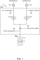
- FIG. 1 An example of a static transfer switch 10 is shown in Figure 1 . As shown, two different electrical power sources 12A, 12B are coupled to the static transfer switch 10. The output of the static transfer switch 10 is coupled to an electrical load 14. Typically, the output is directly connected to a Power Distribution Unit (PDU) 14, which includes a transformer 16. The final electrical load may be racks of computer servers 30 ( Figure 2 ) in a data center. However, it is understood that static transfer switches 10 may also be used to supply power to other types of electrical loads.
- PDU Power Distribution Unit
- the static transfer switch 10 may include a variety of sensors 18A, 18B, 20A, 20B to monitor electrical properties of the first and second power sources 12A, 12B and the power output. For example, it may be desirable to monitor the voltage 18A, 18B of each of the power sources 12A, 12B and to monitor current 20A and voltage 20B of the output.
- the static transfer switch 10 also includes one or more switches 22A, 22B associated with each of the power sources 12A, 12B. This allows the static transfer switch 10 to supply power to the output from either of the power sources 12A, 12B.
- the first power source 12A may be the preferred power source 12A (e.g., the grid)
- the second power source 12B may be a backup power source 12B (e.g., a generator).
- power can be supplied from the first power source 12A to the load 14 by closing the first switch 22A and opening the second switch 22B (to disconnect the second power source 12B).
- the power supply can be transferred to the second power source 12B by opening the first switch 22A and closing the second switch 22B.
- the electrical load 14 is provided with a constant source of power despite the possibility of degraded performance events in one of the power sources 12A, 12B.
- a static transfer switch for increasing the speed of switching from one power source to another power source.
- the system senses degraded performance of the power source supplying power to the load.
- the system turns off a gate signal to a first switch coupled between the power source and the load.
- the system also closes a third switch coupled between an energy storage and the first switch to release a current to the input or output of the first switch The current forces a drop in current conducted through the first switch and causes the first switch to open and stop conducting current.
- the first switch may be opened substantially faster than in conventional static transfer switches.
- FIG. 2 An example of a three-phase static transfer switch 10 is shown in Figure 2 .
- static transfer switches 10 are designed to complete a switching event between the two power sources 12A, 12B within one electrical cycle of the power sources 12A, 12B. This is desirable so that a high-quality, constant power supply is provided with minimal effect on the electrical load 14, 30.
- solid-state switches 22A, 22B first switches 22A and second switches 22B
- the switches 22A, 22B are silicon controlled rectifiers (SCR).
- thyristors may be used for the solid-state switches 22A, 22B, such as integrated gate-commutated thyristors (IGCT), reverse blocking integrated gate-commutated thyristors (RB-IGCT), or gate turn-off thyristors (GTO).
- IGCT integrated gate-commutated thyristors
- RB-IGCT reverse blocking integrated gate-commutated thyristors
- GTO gate turn-off thyristors
- each of the main switches 22A, 22B will be made up of multiple individual switches 26, with at least one switch 26 for each phase A, B, C.
- a pair of anti-parallel thyristors 26 is particularly well-suited for each switch 26 associated with a phase A, B, C.
- each switch 26 typically includes two switches 26A, 26B in an anti-parallel arrangement. However, each pair of anti-parallel thyristors 26A, 26B are often treated as a single switch 26 because they typically turn on and off together.
- the static transfer switch 10 may also include a series of manual switches 28 that are primarily used during maintenance to isolate sections of the circuit.
- first and/or second power sources 12A, 12B prefferably include an uninterruptible power supply (UPS) 32 to provide control over the electrical properties of the original source 12A, 12B and manage power drops or losses in the original source 12A, 12B.
- UPS uninterruptible power supply
- the output is typically coupled to the transformer 16 of a PDU 14, and the final electrical load 30 is often racks of computer servers 30 in a data center.
- An improvement of the invention herein is that it uses a resonant turn off topology adjusted to force commutate a three-phase power system and is operated by an embedded digital processor controlling the signals with software intelligence and algorithms in order to achieve autonomy and make possible a sub-millisecond transfer switch.
- the turn off circuit 40 with RTO topology is shown in Figure 3 .
- the circuit 40 includes a main circuit 42 and a resonant circuit 44.
- the main thyristors 26A, 26B (first switches) are S m1 and S m2 .
- the resonant circuit includes four auxiliary thyristor switches 34 (third switches) S r1 , S r2 , S r3 , S r4 , resonant capacitor C (energy storage) 36, and resonant inductor L 38.
- the capacitor C 36 is pre-charged to provide resonant current to create a zero-current crossing for the main thyristors 26.
- the inductor L 38 limits di/dt for main thyristors 26 during turn-off.
- main thyristors S m1 (or S m2 ) 26A, 26B are conducting and all the auxiliary switches 34 are off.
- the pre-charged resonant capacitor 36 is isolated from the main thyristor switches 26.
- the auxiliary switches 34 S r1,2 (or S r3,4 depending on current direction) are triggered to open by sending a gate signal thereto. As a result, the energy stored in the resonant capacitor 36 is discharged.
- the capacitor 36 voltage provides a negative bias voltage to help the main thyristor 26 turn off (i.e., open and stop conducting).
- the main thyristor 26 current reaches zero, it starts turning off with reverse bias voltage from the resonant capacitor 36.
- resonant capacitance value C pre-charged initial capacitor voltage V c0
- resonant inductance value L there are three possible design choices to control performance: resonant capacitance value C, pre-charged initial capacitor voltage V c0 , and resonant inductance value L. These parameters can be used to determine how much and how fast the main thyristor current can be turned off, as well as the size and cost of the auxiliary resonant circuit.
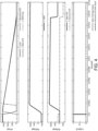
- Figure 4 shows the voltage and current waveforms of resonant turn-off operation for the main thyristors 26 and auxiliary switches 34.
- a gate signal is sent to turn off the main thyristor 26, and a gate signal is sent to turn on the auxiliary thyristors 34. This occurs as a result of degraded performance being identified by a sensor 18, 20.
- the second switches 22B cannot be closed to switch power to the second power source 12B until the first switches 22A have been opened, it would be beneficial to be able to stop current conduction through the first switches 22A faster than in a conventional static transfer switch.
- the resonance starts and the resonant current through L 38 increases fast.
- the main thyristor 26 current decreases to zero and starts turning off.
- the load 14, 16 current is commutated or bypassed to the auxiliary circuit 44 (34, 36, 38).
- the resonant capacitor 36 is re-charged by the load 14, 16 current but in reversed voltage polarity.
- the auxiliary thyristors 34 are turned off. As a result, the RTO has disconnected the first power source 12A and the load 14, 16 is ready to be transferred to the alternative power source 12B.
- the resonant circuits 44 (one for each phase) are shown in Figure 5 .
- a pre-charge circuit 46 is coupled to the resonant circuits 44 with a DC bus 48.
- the DC bus 48 is pre-charged slowly through the single bridge rectifier diodes 50 with resistors 52 to make sure capacitive inrush is prevented.
- a bleeding resistor 54 can be used to adjust that DC level to the desired value.
- a pre-charge relay 56 and bleed relay 58 are used to turn on and off the pre-charging and bleeding.
- a fourth switch 60 is provided between the pre-charge circuit 46 and the capacitors 36 to disconnect the pre-charge circuit 46 from the capacitors. The fourth switch 60 is preferably opened to stop charging of the capacitors in response to the switching event. If desired, fourth switches 60 may be provided for each resonant circuit 44 to disconnect the respective circuit 44 from the DC bus 48.
- a phase locked loop (PLL) 62 (see Figure 9 ) is used to determine the frequency and phase angle of the AC waveform of the power source 12A.
- the PLL 62 can be used in determining the firing sequence for the auxiliary switches 34 because the switches 34 need to be fired at the correct polarity. Since this is a three-phase system, the polarity of phase A, phase B and phase C will not be the same at the same time.
- the firing sequence is determined by the following algorithm:
- auxiliary switches 34 are turned on to release current from the capacitor 36, with one switch 34 being coupled to the input of the main thyristors 26 and the other switch 34 being coupled to the output of the main thyristors 26.
- the two auxiliary switches 34 that are turned on depends on current flow of the AC current through the main switches 26. Thus, when the current is positive, one pair of switches 34 will be turned on (while the other pair remains off), and when the current is negative, the other pair of switches 34 will be turned on (again, with the other pair remaining off).
- all of the main switches 22A, 26 are turned off (i.e., opened) and the auxiliary switches 34 are turned on (i.e., closed) at the same time in the static transfer switch 10. Because some phases A, B, C will have a positive current and some phases A, B, C will have a negative current at the switching instant, the pair of auxiliary switches 34 that is closed in each phase resonant circuit 44 will vary depending on the current of the particular phase A, B, C.
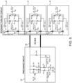
- the main circuits 42 are shown in Figure 6 .
- the table below lists the names of the signals used in the main circuits 42 and the resonant circuits 44 of Figures 5-6 .
- a DSP 64 ( Figures 2 and 8-9 ) may be used to generate the control signals used by the main circuits 42 and resonant circuits 44.
- FIG. 7 shows a flowchart of the method of transferring the power supply for the load 14 from one power source 12A to another power source 12B in a static transfer switch 10.
- the method may be implemented by a controller 64, which may be in the form of a DSP 64.
- steps 66-68 the energy storage (capacitors 36) are precharged by the charging circuit 46.
- the voltage of the DC bus 48 between the charging circuit 46 and the resonant circuits 44 is monitored and controlled to maintain a desired charge on the capacitors 36. That is, the relays 56, 58 are opened and closed as needed to supply voltage and bleed voltage to charge the capacitors 36.
- the quality of the power being supplied by the power source 12A connected to the load 14 is monitored for degraded performance events.
- the main switches 26 for the first power source 12A are opened to disconnect the first power source 12A from the load 14 in steps 72-78. That is, in step 72 turn off gate signals are sent to the main switches 26.
- the auxiliary switches 34 that must be turned on in each resonant circuit 44 are then determined in step 74 by phase locked loops 62 (see OUT_RTO_MINUS, OUT_RTO_PLUS algorithm above).
- the auxiliary switches 34 that have been determined in step 74 are then turned on with gate signals in step 76.
- step 78 the DSP 64 verifies that the preferred power source 12A is completely disconnected by confirming that the net value of the current and voltage passing through the main switches 22A, 26 for each phase of the preferred power source 12A is zero or negligible enough to confirm that the resonant circuits 44 did in fact reverse the bias for each of the main circuits 42.
- the DSP 64 can initiate a turn on command to the alternate power source 12B in step 80. Due to power quality considerations like inrush and soft start and preferred turn on conditions, it is possible to vary the method used to turn on the second power source 12B while still making use of the improved method of turning off the main switches 26 of the first power source 12A. After the main switches 22B, 26 for the alternate power source 12 have been turned on, the power transfer has been completed in step 82.
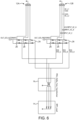
- FIGS 8-9 show a control system that may be used to control the resonant circuits 44, and associated charging circuit 46. It is understood that the control system may also be used to control the main circuits 42 as well.
- the Digital Signal Processor (DSP) 64 may be used to control all the relays, sense the voltages for the PLL synchronization and control the main switches 26, 42 and RTO thyristors 34, 44.
- a scaling processor 84 may be provided to adjust the inputs for use by the DSP 64.
- the DSP 64 may include a PLL element 62 and a phase decoder element 86 to evaluate the current direction of each phase and generate the gate signals for the auxiliary switches 34.
Landscapes
- Engineering & Computer Science (AREA)
- Power Engineering (AREA)
- Business, Economics & Management (AREA)
- Emergency Management (AREA)
- Stand-By Power Supply Arrangements (AREA)
- Electronic Switches (AREA)
Claims (16)
- Statischer Umschalter (10), Folgendes umfassend:eine Menge erster Leistungseingänge, die mit einer ersten dreiphasigen elektrischen Leistungsquelle (12A) verbunden sind, wobei jeder der ersten Leistungseingänge mit einer Phase der ersten dreiphasigen elektrischen Leistungsquelle (12A) verbunden ist;eine Menge zweiter Leistungseingänge, die mit einer zweiten dreiphasigen elektrischen Leistungsquelle (12B) verbunden sind, wobei jeder der zweiten Leistungseingänge mit einer Phase der zweiten dreiphasigen elektrischen Leistungsquelle (12B) verbunden ist;eine Menge von Leistungsausgängen, die mit einer dreiphasigen elektrischen Last (14) verbunden sind, wobei jeder der Leistungsausgänge mit einer Phase der dreiphasigen elektrischen Last (14) verbunden ist;eine Menge erster Schalter (22A), die zwischen der Menge erster Leistungseingänge und der Menge von Leistungsausgängen geschaltet sind;eine Menge zweiter Schalter (22B), die zwischen der Menge zweiter Leistungseingänge und der Menge von Leistungsausgängen geschaltet sind;eine Menge von dritten Thyristorschaltern (34), die zwischen einem Energiespeicher (36) und der Menge von ersten Schaltern (22A) gekoppelt sind, wobei die Menge von dritten Thyristorschaltern (34) eine Gleichrichterbrücke bildet, wobei der Energiespeicher (36) zwischen dem Plus-Anschluss und dem Minus-Anschluss der Brücke angeordnet ist, wobei jeder dritte Thyristorschalter (34) zwischen dem Energiespeicher (36) und einem jeweiligen ersten Schalter (22A, 26) gekoppelt ist;einen Sensor (18A) zur Bestimmung einer elektrischen Eigenschaft der ersten dreiphasigen elektrischen Stromquelle (12A);einen Leistungsübertragungsregler (64), wobei der Sensor (18A) ein Signal an einen Eingang des Leistungsübertragungsreglers (64) liefert und die Mengen der ersten Schalter (22A) und zweiten Schalter (22B) Signale an Ausgänge des Leistungsübertragungsreglers (64) liefern;eine Ladeschaltung (46) zur Aufrechterhaltung einer vorgegebenen Ladung des Energiespeichers (36); undeinen vierten Schalter (60), der zwischen den Energiespeicher (36) und die Ladeschaltung (46) geschaltet ist;wobei während eines normalen Betriebs die Leistungsübertragungssteuerung (64) die Menge erster Schalter (22A) schließt, um die Menge erster Leistungseingänge und die Menge von Leistungsausgängen elektrisch miteinander zu verbinden, und die Menge zweiter Schalter (22B) öffnet, um die Menge zweiter Leistungseingänge und der Menge von Leistungsausgängen elektrisch zu trennen, wobei die erste dreiphasige elektrische Stromquelle (12A) dadurch Strom an die dreiphasige elektrische Last (14) liefert;wobei, wenn der Sensor eine verschlechterte Leistung der ersten dreiphasigen elektrischen Stromquelle (12A) identifiziert, der Leistungsübertragungsregler (64) zum Einleiten eines Schaltvorgangs konfiguriert ist, wobei der Schaltvorgang die folgenden Schritte umfasst:Öffnen des vierten Schalters (60), um das Laden des Energiespeichers (36) zu stoppen, wenn der Sensor eine verschlechterte Leistung der ersten dreiphasigen elektrischen Stromquelle (12A) feststellt;Ausschalten eines Gate-Signals für jeden der ersten Schalter (22A);Schließen jedes der dritten Thyristorschalter (34), nachdem das Gate-Signal des jeweiligen ersten Schalters (22A, 26) ausgeschaltet wurde, wobei der Energiespeicher (36) dadurch einen Strom an den Eingang oder den Ausgang des jeweiligen ersten Schalters (22A, 26) liefert, um einen Stromabfall zu erzwingen, der durch den jeweiligen ersten Schalter (22A, 26) geleitet wird, wobei der Stromabfall bewirkt, dass sich der jeweilige erste Schalter (22A, 26) öffnet und aufhört, Strom zwischen der ersten dreiphasigen elektrischen Energiequelle (12A) und der dreiphasigen elektrischen Last (14) durch ihn zu leiten; undSchließen der Menge von zweiten Schaltern (22B), nachdem die entsprechenden ersten Schalter (22A) geöffnet wurden, wobei die zweite dreiphasige elektrische Stromquelle (12B) dadurch Strom an die dreiphasige elektrische Last (14) liefert.
- Statischer Umschalter (10) nach Anspruch 1,
wobei das Schaltereignis innerhalb eines elektrischen Zyklus der zweiten dreiphasigen elektrischen Stromquelle (12B) auftritt. - Statischer Umschalter (10) nach Anspruch 1,
wobei die Menge von ersten Schaltern (22A) siliziumgesteuerte Gleichrichter umfasst. - Statischer Umschalter (10) nach Anspruch 1,
wobei die Menge von ersten Schaltern (22A) integrierte gate-kommutierte Thyristoren (IGCT), sperrende integrierte gate-kommutierte Thyristoren (IGCT) oder gate-abschaltende Thyristoren (GTO) umfasst. - Statischer Umschalter (10) nach Anspruch 1,
wobei die Menge von Leistungsausgängen mit einem Transformator (16) gekoppelt ist. - Statischer Umschalter (10) nach Anspruch 1,
wobei die dreiphasige elektrische Last (14) ein Rechenzentrum umfasst. - Statischer Umschalter (10) nach Anspruch 1,
wobei eine der ersten und zweiten dreiphasigen Stromquellen (12B) eine unterbrechungsfreie Stromversorgung (USV) umfasst. - Statischer Umschalter (10) nach Anspruch 1,
wobei jeder der dritten Schalter (34) zur gleichen Zeit geschlossen wird. - Statischer Umschalter (10) nach Anspruch 1,
ferner aufweisend zwei der dritten Schalter (34), die mit jedem der ersten Schalter (22A) gekoppelt sind, wobei einer der dritten Schalter (34) mit dem Eingang des jeweiligen ersten Schalters (22A, 26) und der andere der dritten Schalter (34) mit dem Ausgang des jeweiligen ersten Schalters (22A, 26) gekoppelt ist, wobei der Energiespeicher (36) zwischen den beiden dritten Schaltern (34) angeordnet ist. - Statischer Umschalter (10) nach Anspruch 1,ferner aufweisend zwei der dritten Schalter (34), die mit jedem der ersten Schalter (22A) gekoppelt sind, wobei die beiden dritten Schalter (34) beide zwischen dem Energiespeicher (36) und dem Eingang oder dem Ausgang des jeweiligen ersten Schalters (22A, 26) angeordnet sind,wobei einer der beiden dritten Schalter (34) geschlossen ist, wenn ein positiver Strom durch den jeweiligen dritten Schalter (34) geleitet wird, und ein anderer der beiden dritten Schalter (34) geschlossen ist, wenn ein positiver Strom durch den jeweiligen dritten Schalter (34) geleitet wird.
- Statischer Umschalter (10) nach Anspruch 1,ferner aufweisend vier der dritten Schalter (34), die mit jedem der ersten Schalter (22A) gekoppelt sind, wobei zwei der dritten Schalter (34) mit dem Eingang des jeweiligen ersten Schalters (22A, 26) und zwei der dritten Schalter (34) mit dem Ausgang des jeweiligen ersten Schalters (22A, 26) gekoppelt sind, wobei der Energiespeicher (36) zwischen zwei der dritten Schalter (34) auf einer Seite und zwei der dritten Schalter (34) auf einer anderen Seite angeordnet ist,wobei zwei der dritten Schalter (34) auf gegenüberliegenden Seiten des Energiespeichers (36) geschlossen sind, wenn ein positiver Strom durch den jeweiligen dritten Schalter (34) geleitet wird, und zwei andere der dritten Schalter (34) auf gegenüberliegenden Seiten des Energiespeichers (36) geschlossen sind, wenn ein negativer Strom durch den jeweiligen dritten Schalter (34) geleitet wird.
- Statischer Umschalter (10) nach Anspruch 1,
ferner aufweisend eine Induktionsspule, die zwischen den Eingang oder Ausgang jedes ersten Schalters (22A, 26) und den jeweiligen dritten Schalter (34) geschaltet ist. - Statischer Umschalter (10) nach Anspruch 1,
wobei der Energiespeicher (36) ein Kondensator ist. - Statischer Umschalter (10) nach Anspruch 1,
wobei der von dem Energiespeicher (36) abgegebene Strom und der durch den jeweiligen ersten Schalter (22A, 26) geleitete Strom innerhalb von 0,5 ms nach dem Ausschalten des Gatesignals für den jeweiligen ersten Schalter (22A, 26) und dem Schließen des jeweiligen dritten Schalters (34) aufhört, zu der dreiphasigen elektrischen Last (14) zu fließen. - Statischer Umschalter (10) nach Anspruch 1,wobei die Menge von ersten Schaltern (22A) siliziumgesteuerte Gleichrichter umfasst, ferner umfassend vier der dritten Schalter (34), die mit jedem der ersten Schalter (22A) gekoppelt sind, wobei zwei der dritten Schalter (34) mit dem Eingang des jeweiligen ersten Schalters (22A, 26) und zwei der dritten Schalter (34) mit dem Ausgang des jeweiligen ersten Schalters (22A, 26) gekoppelt sind, wobei der Energiespeicher (36) zwischen den zwei der dritten Schalter (34) auf einer Seite und zwei der dritten Schalter (34) auf einer anderen Seite angeordnet ist,wobei zwei der dritten Schalter (34) auf gegenüberliegenden Seiten des Energiespeichers (36) geschlossen sind, wenn ein positiver Strom durch den jeweiligen dritten Schalter (34) geleitet wird, und zwei andere der dritten Schalter (34) auf gegenüberliegenden Seiten des Energiespeichers (36) geschlossen sind, wenn ein negativer Strom durch den jeweiligen dritten Schalter (34) geleitet wird,wobei der Energiespeicher (36) separate Kondensatoren umfasst, die mit jedem der ersten Schalter (22A) verbunden sind.
- Statischer Umschalter (10) nach Anspruch 15,ferner aufweisend einen Induktor, der zwischen den Eingang oder Ausgang jedes ersten Schalters (22A, 26) und den jeweiligen dritten Schalter (34) gekoppelt ist,eine Ladeschaltung (46), um eine vorbestimmte Ladung der getrennten Kondensatoren aufrechtzuerhalten, undeine Menge von vierten Schaltern (60), wobei jeder vierte Schalter (60) zwischen einen der getrennten Kondensatoren und die Ladeschaltung (46) gekoppelt ist, umfasst wobei die Leistungsübertragungssteuerung (64) den jeweiligen vierten Schalter (60) öffnet, um das Laden des jeweiligen separaten Kondensators als Reaktion darauf zu stoppen, dass der Sensor eine verschlechterte Leistung der ersten dreiphasigen elektrischen Stromquelle (12A) identifiziert, wobei jeder der vierten Schalter (60) geöffnet wird, bevor die jeweiligen dritten Schalter (34) geschlossen werden.
Applications Claiming Priority (2)
| Application Number | Priority Date | Filing Date | Title |
|---|---|---|---|
| US16/521,694 US10903649B1 (en) | 2019-07-25 | 2019-07-25 | Static transfer switch with turn off circuit |
| PCT/US2020/041484 WO2021015962A1 (en) | 2019-07-25 | 2020-07-10 | Static transfer switch with turn off circuit |
Publications (3)
| Publication Number | Publication Date |
|---|---|
| EP4005058A1 EP4005058A1 (de) | 2022-06-01 |
| EP4005058A4 EP4005058A4 (de) | 2023-09-06 |
| EP4005058B1 true EP4005058B1 (de) | 2024-11-27 |
Family
ID=74190512
Family Applications (1)
| Application Number | Title | Priority Date | Filing Date |
|---|---|---|---|
| EP20843009.0A Active EP4005058B1 (de) | 2019-07-25 | 2020-07-10 | Statischer transferschalter mit abschaltkreis |
Country Status (4)
| Country | Link |
|---|---|
| US (1) | US10903649B1 (de) |
| EP (1) | EP4005058B1 (de) |
| CN (1) | CN114207983B (de) |
| WO (1) | WO2021015962A1 (de) |
Families Citing this family (9)
| Publication number | Priority date | Publication date | Assignee | Title |
|---|---|---|---|---|
| US11211816B1 (en) * | 2020-11-20 | 2021-12-28 | Abb Schweiz Ag | Delta connected resonant turn off circuits |
| US11683031B1 (en) | 2021-12-23 | 2023-06-20 | Abb Schweiz Ag | Thyristor current interrupter |
| CN117375194A (zh) * | 2022-06-30 | 2024-01-09 | 施耐德电器工业公司 | 混合式快速转换开关及利用其在电源间快速切换的方法 |
| US11923724B2 (en) * | 2022-07-21 | 2024-03-05 | Abb Schweiz Ag | Systems and methods for self-learning of transformer inrush characteristics to optimize transfer times in static transfer switch |
| US12184077B2 (en) * | 2022-10-19 | 2024-12-31 | Abb Schweiz Ag | Convertible transfer switch |
| CN115931024B (zh) * | 2022-12-30 | 2025-12-19 | Abb瑞士股份有限公司 | 传感器设备和电气设备 |
| US20250088029A1 (en) * | 2023-09-08 | 2025-03-13 | Abb Schweiz Ag | Static transfer switches with intelligent bypass |
| US20250330017A1 (en) * | 2024-04-22 | 2025-10-23 | Abb Schweiz Ag | Static transfer switch with automatic startup |
| WO2025245469A1 (en) * | 2024-05-24 | 2025-11-27 | Watlow Electric Manufacturing Company | Method and system for digital real-time communications in thyristor-based power controllers |
Family Cites Families (12)
| Publication number | Priority date | Publication date | Assignee | Title |
|---|---|---|---|---|
| US6118676A (en) * | 1998-11-06 | 2000-09-12 | Soft Switching Technologies Corp. | Dynamic voltage sag correction |
| US6560128B1 (en) * | 1999-02-12 | 2003-05-06 | Satcon Power Systems Canada Ltd. | Ferroresonance-suppressing static transfer switch |
| US7459804B2 (en) | 2004-02-10 | 2008-12-02 | Liebert Corporation | Static transfer switch device and method |
| US7589438B2 (en) | 2004-07-09 | 2009-09-15 | Layerzero Power Systems, Inc. | Source phase sensitive transfer method and apparatus |
| US7265458B2 (en) * | 2005-04-08 | 2007-09-04 | Eaton Power Quality Corporation | Apparatus and methods for coordinated static switch operations for load transfers in uninterruptible power supply systems |
| KR101079900B1 (ko) * | 2007-10-31 | 2011-11-04 | 주식회사 케이티 | 선택스위치 장치, 이를 이용한 전원공급장치 및 그 스위칭 방법 |
| GB0724369D0 (en) * | 2007-12-13 | 2008-01-30 | Univ Aberdeen | Power converter |
| CN101854075B (zh) | 2010-05-27 | 2012-09-05 | Asco电力技术公司 | 一种灭弧混合切换开关及开关切换方法 |
| CN102820699B (zh) * | 2012-08-09 | 2014-06-11 | 常熟瑞特电气股份有限公司 | 一种智能数字式静态开关 |
| JP6953885B2 (ja) * | 2017-08-10 | 2021-10-27 | 富士電機株式会社 | 電源装置および遮断スイッチ回路 |
| CN107786188B (zh) * | 2017-10-25 | 2020-09-08 | 清华大学 | 基于lc振荡强迫换流型复合式开关 |
| CN107769369B (zh) * | 2017-10-25 | 2019-10-25 | 清华大学 | 一种基于耦合负压电路的混合式开关 |
-
2019
- 2019-07-25 US US16/521,694 patent/US10903649B1/en active Active
-
2020
- 2020-07-10 WO PCT/US2020/041484 patent/WO2021015962A1/en not_active Ceased
- 2020-07-10 EP EP20843009.0A patent/EP4005058B1/de active Active
- 2020-07-10 CN CN202080053406.XA patent/CN114207983B/zh active Active
Also Published As
| Publication number | Publication date |
|---|---|
| CN114207983A (zh) | 2022-03-18 |
| EP4005058A4 (de) | 2023-09-06 |
| WO2021015962A1 (en) | 2021-01-28 |
| CN114207983B (zh) | 2024-03-01 |
| EP4005058A1 (de) | 2022-06-01 |
| US20210028621A1 (en) | 2021-01-28 |
| US10903649B1 (en) | 2021-01-26 |
Similar Documents
| Publication | Publication Date | Title |
|---|---|---|
| EP4005058B1 (de) | Statischer transferschalter mit abschaltkreis | |
| US11211816B1 (en) | Delta connected resonant turn off circuits | |
| EP4002693A1 (de) | Resonante kommutierungsschaltung die von mehreren halbleiterschaltern genutzt wird | |
| CA2577524C (en) | Power converter with active discharging for improved auto-restart capability | |
| EP4107860B1 (de) | Thyristorstromunterbrecher und quasi resonante hilfsabschaltungseinheit | |
| US20030227785A1 (en) | On-line uninterruptible power supplies with two-relay bypass circuit and methods of operation thereof | |
| US11171508B2 (en) | System and method for shared hybrid transfer switch | |
| CN106602636A (zh) | 电池系统 | |
| CN116998079A (zh) | 浪涌电流限制变压器通电装置、方法、系统和技术 | |
| CN113544623A (zh) | 具有谐振关断的静态转换开关 | |
| CN114257104B (zh) | 主动换相单元以及强迫换相的混合式换流器拓扑结构 | |
| EP3127232B1 (de) | Hocheffiziente kommutierungsschaltung | |
| CN109983681A (zh) | 用于控制基于晶闸管开关元件的开关模块的方法 | |
| CN117375199A (zh) | 电源转换电路 | |
| US20250112458A1 (en) | Transformer energization with low inrush current | |
| JP4042092B2 (ja) | 電力変換システム | |
| JPS6248232A (ja) | 超電導エネルギ転送回路 | |
| JPH0541354U (ja) | 超電導エネルギ貯蔵装置 |
Legal Events
| Date | Code | Title | Description |
|---|---|---|---|
| STAA | Information on the status of an ep patent application or granted ep patent |
Free format text: STATUS: THE INTERNATIONAL PUBLICATION HAS BEEN MADE |
|
| PUAI | Public reference made under article 153(3) epc to a published international application that has entered the european phase |
Free format text: ORIGINAL CODE: 0009012 |
|
| STAA | Information on the status of an ep patent application or granted ep patent |
Free format text: STATUS: REQUEST FOR EXAMINATION WAS MADE |
|
| 17P | Request for examination filed |
Effective date: 20220125 |
|
| AK | Designated contracting states |
Kind code of ref document: A1 Designated state(s): AL AT BE BG CH CY CZ DE DK EE ES FI FR GB GR HR HU IE IS IT LI LT LU LV MC MK MT NL NO PL PT RO RS SE SI SK SM TR |
|
| DAV | Request for validation of the european patent (deleted) | ||
| DAX | Request for extension of the european patent (deleted) | ||
| A4 | Supplementary search report drawn up and despatched |
Effective date: 20230803 |
|
| RIC1 | Information provided on ipc code assigned before grant |
Ipc: H02J 7/34 20060101ALI20230728BHEP Ipc: H02J 9/08 20060101ALI20230728BHEP Ipc: H02J 9/06 20060101AFI20230728BHEP |
|
| GRAP | Despatch of communication of intention to grant a patent |
Free format text: ORIGINAL CODE: EPIDOSNIGR1 |
|
| STAA | Information on the status of an ep patent application or granted ep patent |
Free format text: STATUS: GRANT OF PATENT IS INTENDED |
|
| INTG | Intention to grant announced |
Effective date: 20240625 |
|
| GRAS | Grant fee paid |
Free format text: ORIGINAL CODE: EPIDOSNIGR3 |
|
| GRAA | (expected) grant |
Free format text: ORIGINAL CODE: 0009210 |
|
| STAA | Information on the status of an ep patent application or granted ep patent |
Free format text: STATUS: THE PATENT HAS BEEN GRANTED |
|
| AK | Designated contracting states |
Kind code of ref document: B1 Designated state(s): AL AT BE BG CH CY CZ DE DK EE ES FI FR GB GR HR HU IE IS IT LI LT LU LV MC MK MT NL NO PL PT RO RS SE SI SK SM TR |
|
| REG | Reference to a national code |
Ref country code: GB Ref legal event code: FG4D |
|
| REG | Reference to a national code |
Ref country code: CH Ref legal event code: EP |
|
| REG | Reference to a national code |
Ref country code: IE Ref legal event code: FG4D |
|
| REG | Reference to a national code |
Ref country code: DE Ref legal event code: R096 Ref document number: 602020042210 Country of ref document: DE |
|
| REG | Reference to a national code |
Ref country code: LT Ref legal event code: MG9D |
|
| REG | Reference to a national code |
Ref country code: NL Ref legal event code: MP Effective date: 20241127 |
|
| PG25 | Lapsed in a contracting state [announced via postgrant information from national office to epo] |
Ref country code: IS Free format text: LAPSE BECAUSE OF FAILURE TO SUBMIT A TRANSLATION OF THE DESCRIPTION OR TO PAY THE FEE WITHIN THE PRESCRIBED TIME-LIMIT Effective date: 20250327 Ref country code: PT Free format text: LAPSE BECAUSE OF FAILURE TO SUBMIT A TRANSLATION OF THE DESCRIPTION OR TO PAY THE FEE WITHIN THE PRESCRIBED TIME-LIMIT Effective date: 20250327 Ref country code: HR Free format text: LAPSE BECAUSE OF FAILURE TO SUBMIT A TRANSLATION OF THE DESCRIPTION OR TO PAY THE FEE WITHIN THE PRESCRIBED TIME-LIMIT Effective date: 20241127 |
|
| PG25 | Lapsed in a contracting state [announced via postgrant information from national office to epo] |
Ref country code: FI Free format text: LAPSE BECAUSE OF FAILURE TO SUBMIT A TRANSLATION OF THE DESCRIPTION OR TO PAY THE FEE WITHIN THE PRESCRIBED TIME-LIMIT Effective date: 20241127 Ref country code: NL Free format text: LAPSE BECAUSE OF FAILURE TO SUBMIT A TRANSLATION OF THE DESCRIPTION OR TO PAY THE FEE WITHIN THE PRESCRIBED TIME-LIMIT Effective date: 20241127 |
|
| REG | Reference to a national code |
Ref country code: AT Ref legal event code: MK05 Ref document number: 1746673 Country of ref document: AT Kind code of ref document: T Effective date: 20241127 |
|
| PG25 | Lapsed in a contracting state [announced via postgrant information from national office to epo] |
Ref country code: BG Free format text: LAPSE BECAUSE OF FAILURE TO SUBMIT A TRANSLATION OF THE DESCRIPTION OR TO PAY THE FEE WITHIN THE PRESCRIBED TIME-LIMIT Effective date: 20241127 |
|
| PG25 | Lapsed in a contracting state [announced via postgrant information from national office to epo] |
Ref country code: ES Free format text: LAPSE BECAUSE OF FAILURE TO SUBMIT A TRANSLATION OF THE DESCRIPTION OR TO PAY THE FEE WITHIN THE PRESCRIBED TIME-LIMIT Effective date: 20241127 |
|
| PG25 | Lapsed in a contracting state [announced via postgrant information from national office to epo] |
Ref country code: NO Free format text: LAPSE BECAUSE OF FAILURE TO SUBMIT A TRANSLATION OF THE DESCRIPTION OR TO PAY THE FEE WITHIN THE PRESCRIBED TIME-LIMIT Effective date: 20250227 |
|
| PG25 | Lapsed in a contracting state [announced via postgrant information from national office to epo] |
Ref country code: GR Free format text: LAPSE BECAUSE OF FAILURE TO SUBMIT A TRANSLATION OF THE DESCRIPTION OR TO PAY THE FEE WITHIN THE PRESCRIBED TIME-LIMIT Effective date: 20250228 Ref country code: AT Free format text: LAPSE BECAUSE OF FAILURE TO SUBMIT A TRANSLATION OF THE DESCRIPTION OR TO PAY THE FEE WITHIN THE PRESCRIBED TIME-LIMIT Effective date: 20241127 Ref country code: LV Free format text: LAPSE BECAUSE OF FAILURE TO SUBMIT A TRANSLATION OF THE DESCRIPTION OR TO PAY THE FEE WITHIN THE PRESCRIBED TIME-LIMIT Effective date: 20241127 |
|
| PG25 | Lapsed in a contracting state [announced via postgrant information from national office to epo] |
Ref country code: PL Free format text: LAPSE BECAUSE OF FAILURE TO SUBMIT A TRANSLATION OF THE DESCRIPTION OR TO PAY THE FEE WITHIN THE PRESCRIBED TIME-LIMIT Effective date: 20241127 |
|
| PG25 | Lapsed in a contracting state [announced via postgrant information from national office to epo] |
Ref country code: RS Free format text: LAPSE BECAUSE OF FAILURE TO SUBMIT A TRANSLATION OF THE DESCRIPTION OR TO PAY THE FEE WITHIN THE PRESCRIBED TIME-LIMIT Effective date: 20250227 |
|
| PG25 | Lapsed in a contracting state [announced via postgrant information from national office to epo] |
Ref country code: SM Free format text: LAPSE BECAUSE OF FAILURE TO SUBMIT A TRANSLATION OF THE DESCRIPTION OR TO PAY THE FEE WITHIN THE PRESCRIBED TIME-LIMIT Effective date: 20241127 |
|
| PG25 | Lapsed in a contracting state [announced via postgrant information from national office to epo] |
Ref country code: DK Free format text: LAPSE BECAUSE OF FAILURE TO SUBMIT A TRANSLATION OF THE DESCRIPTION OR TO PAY THE FEE WITHIN THE PRESCRIBED TIME-LIMIT Effective date: 20241127 |
|
| PG25 | Lapsed in a contracting state [announced via postgrant information from national office to epo] |
Ref country code: EE Free format text: LAPSE BECAUSE OF FAILURE TO SUBMIT A TRANSLATION OF THE DESCRIPTION OR TO PAY THE FEE WITHIN THE PRESCRIBED TIME-LIMIT Effective date: 20241127 |
|
| PG25 | Lapsed in a contracting state [announced via postgrant information from national office to epo] |
Ref country code: RO Free format text: LAPSE BECAUSE OF FAILURE TO SUBMIT A TRANSLATION OF THE DESCRIPTION OR TO PAY THE FEE WITHIN THE PRESCRIBED TIME-LIMIT Effective date: 20241127 |
|
| PG25 | Lapsed in a contracting state [announced via postgrant information from national office to epo] |
Ref country code: SK Free format text: LAPSE BECAUSE OF FAILURE TO SUBMIT A TRANSLATION OF THE DESCRIPTION OR TO PAY THE FEE WITHIN THE PRESCRIBED TIME-LIMIT Effective date: 20241127 |
|
| PG25 | Lapsed in a contracting state [announced via postgrant information from national office to epo] |
Ref country code: CZ Free format text: LAPSE BECAUSE OF FAILURE TO SUBMIT A TRANSLATION OF THE DESCRIPTION OR TO PAY THE FEE WITHIN THE PRESCRIBED TIME-LIMIT Effective date: 20241127 |
|
| PG25 | Lapsed in a contracting state [announced via postgrant information from national office to epo] |
Ref country code: IT Free format text: LAPSE BECAUSE OF FAILURE TO SUBMIT A TRANSLATION OF THE DESCRIPTION OR TO PAY THE FEE WITHIN THE PRESCRIBED TIME-LIMIT Effective date: 20241127 |
|
| REG | Reference to a national code |
Ref country code: DE Ref legal event code: R097 Ref document number: 602020042210 Country of ref document: DE |
|
| PG25 | Lapsed in a contracting state [announced via postgrant information from national office to epo] |
Ref country code: SE Free format text: LAPSE BECAUSE OF FAILURE TO SUBMIT A TRANSLATION OF THE DESCRIPTION OR TO PAY THE FEE WITHIN THE PRESCRIBED TIME-LIMIT Effective date: 20241127 |
|
| PLBE | No opposition filed within time limit |
Free format text: ORIGINAL CODE: 0009261 |
|
| STAA | Information on the status of an ep patent application or granted ep patent |
Free format text: STATUS: NO OPPOSITION FILED WITHIN TIME LIMIT |
|
| REG | Reference to a national code |
Ref country code: CH Ref legal event code: L10 Free format text: ST27 STATUS EVENT CODE: U-0-0-L10-L00 (AS PROVIDED BY THE NATIONAL OFFICE) Effective date: 20251008 |
|
| PGFP | Annual fee paid to national office [announced via postgrant information from national office to epo] |
Ref country code: DE Payment date: 20250722 Year of fee payment: 6 |
|
| PGFP | Annual fee paid to national office [announced via postgrant information from national office to epo] |
Ref country code: GB Payment date: 20250722 Year of fee payment: 6 |
|
| 26N | No opposition filed |
Effective date: 20250828 |
|
| REG | Reference to a national code |
Ref country code: CH Ref legal event code: H13 Free format text: ST27 STATUS EVENT CODE: U-0-0-H10-H13 (AS PROVIDED BY THE NATIONAL OFFICE) Effective date: 20260224 |
|
| PG25 | Lapsed in a contracting state [announced via postgrant information from national office to epo] |
Ref country code: LU Free format text: LAPSE BECAUSE OF NON-PAYMENT OF DUE FEES Effective date: 20250710 |
|
| REG | Reference to a national code |
Ref country code: BE Ref legal event code: MM Effective date: 20250731 |
|
| PG25 | Lapsed in a contracting state [announced via postgrant information from national office to epo] |
Ref country code: BE Free format text: LAPSE BECAUSE OF NON-PAYMENT OF DUE FEES Effective date: 20250731 |
|
| PG25 | Lapsed in a contracting state [announced via postgrant information from national office to epo] |
Ref country code: FR Free format text: LAPSE BECAUSE OF NON-PAYMENT OF DUE FEES Effective date: 20250731 |
|
| PG25 | Lapsed in a contracting state [announced via postgrant information from national office to epo] |
Ref country code: CH Free format text: LAPSE BECAUSE OF NON-PAYMENT OF DUE FEES Effective date: 20250731 |