EP4007000B1 - Halbleiterbauelement - Google Patents
Halbleiterbauelement Download PDFInfo
- Publication number
- EP4007000B1 EP4007000B1 EP21183408.0A EP21183408A EP4007000B1 EP 4007000 B1 EP4007000 B1 EP 4007000B1 EP 21183408 A EP21183408 A EP 21183408A EP 4007000 B1 EP4007000 B1 EP 4007000B1
- Authority
- EP
- European Patent Office
- Prior art keywords
- layer
- phase change
- change material
- selection device
- chalcogen
- Prior art date
- Legal status (The legal status is an assumption and is not a legal conclusion. Google has not performed a legal analysis and makes no representation as to the accuracy of the status listed.)
- Active
Links
Images


Classifications
-
- H—ELECTRICITY
- H10—SEMICONDUCTOR DEVICES; ELECTRIC SOLID-STATE DEVICES NOT OTHERWISE PROVIDED FOR
- H10N—ELECTRIC SOLID-STATE DEVICES NOT OTHERWISE PROVIDED FOR
- H10N70/00—Solid-state devices having no potential barriers, and specially adapted for rectifying, amplifying, oscillating or switching
- H10N70/801—Constructional details of multistable switching devices
- H10N70/881—Switching materials
- H10N70/882—Compounds of sulfur, selenium or tellurium, e.g. chalcogenides
- H10N70/8822—Sulfides, e.g. CuS
-
- H—ELECTRICITY
- H10—SEMICONDUCTOR DEVICES; ELECTRIC SOLID-STATE DEVICES NOT OTHERWISE PROVIDED FOR
- H10B—ELECTRONIC MEMORY DEVICES
- H10B63/00—Resistance change memory devices, e.g. resistive RAM [ReRAM] devices
- H10B63/20—Resistance change memory devices, e.g. resistive RAM [ReRAM] devices comprising selection components having two electrodes, e.g. diodes
- H10B63/24—Resistance change memory devices, e.g. resistive RAM [ReRAM] devices comprising selection components having two electrodes, e.g. diodes of the Ovonic threshold switching type
-
- H—ELECTRICITY
- H10—SEMICONDUCTOR DEVICES; ELECTRIC SOLID-STATE DEVICES NOT OTHERWISE PROVIDED FOR
- H10B—ELECTRONIC MEMORY DEVICES
- H10B63/00—Resistance change memory devices, e.g. resistive RAM [ReRAM] devices
- H10B63/80—Arrangements comprising multiple bistable or multi-stable switching components of the same type on a plane parallel to the substrate, e.g. cross-point arrays
- H10B63/84—Arrangements comprising multiple bistable or multi-stable switching components of the same type on a plane parallel to the substrate, e.g. cross-point arrays arranged in a direction perpendicular to the substrate, e.g. 3D cell arrays
- H10B63/845—Arrangements comprising multiple bistable or multi-stable switching components of the same type on a plane parallel to the substrate, e.g. cross-point arrays arranged in a direction perpendicular to the substrate, e.g. 3D cell arrays the switching components being connected to a common vertical conductor
-
- H—ELECTRICITY
- H10—SEMICONDUCTOR DEVICES; ELECTRIC SOLID-STATE DEVICES NOT OTHERWISE PROVIDED FOR
- H10N—ELECTRIC SOLID-STATE DEVICES NOT OTHERWISE PROVIDED FOR
- H10N70/00—Solid-state devices having no potential barriers, and specially adapted for rectifying, amplifying, oscillating or switching
- H10N70/011—Manufacture or treatment of multistable switching devices
- H10N70/061—Shaping switching materials
- H10N70/066—Shaping switching materials by filling of openings, e.g. damascene method
-
- H—ELECTRICITY
- H10—SEMICONDUCTOR DEVICES; ELECTRIC SOLID-STATE DEVICES NOT OTHERWISE PROVIDED FOR
- H10N—ELECTRIC SOLID-STATE DEVICES NOT OTHERWISE PROVIDED FOR
- H10N70/00—Solid-state devices having no potential barriers, and specially adapted for rectifying, amplifying, oscillating or switching
- H10N70/20—Multistable switching devices, e.g. memristors
- H10N70/231—Multistable switching devices, e.g. memristors based on solid-state phase change, e.g. between amorphous and crystalline phases, Ovshinsky effect
- H10N70/235—Multistable switching devices, e.g. memristors based on solid-state phase change, e.g. between amorphous and crystalline phases, Ovshinsky effect between different crystalline phases, e.g. cubic and hexagonal
-
- H—ELECTRICITY
- H10—SEMICONDUCTOR DEVICES; ELECTRIC SOLID-STATE DEVICES NOT OTHERWISE PROVIDED FOR
- H10N—ELECTRIC SOLID-STATE DEVICES NOT OTHERWISE PROVIDED FOR
- H10N70/00—Solid-state devices having no potential barriers, and specially adapted for rectifying, amplifying, oscillating or switching
- H10N70/801—Constructional details of multistable switching devices
- H10N70/821—Device geometry
- H10N70/823—Device geometry adapted for essentially horizontal current flow, e.g. bridge type devices
-
- H—ELECTRICITY
- H10—SEMICONDUCTOR DEVICES; ELECTRIC SOLID-STATE DEVICES NOT OTHERWISE PROVIDED FOR
- H10N—ELECTRIC SOLID-STATE DEVICES NOT OTHERWISE PROVIDED FOR
- H10N70/00—Solid-state devices having no potential barriers, and specially adapted for rectifying, amplifying, oscillating or switching
- H10N70/801—Constructional details of multistable switching devices
- H10N70/841—Electrodes
- H10N70/8413—Electrodes adapted for resistive heating
-
- H—ELECTRICITY
- H10—SEMICONDUCTOR DEVICES; ELECTRIC SOLID-STATE DEVICES NOT OTHERWISE PROVIDED FOR
- H10N—ELECTRIC SOLID-STATE DEVICES NOT OTHERWISE PROVIDED FOR
- H10N70/00—Solid-state devices having no potential barriers, and specially adapted for rectifying, amplifying, oscillating or switching
- H10N70/801—Constructional details of multistable switching devices
- H10N70/881—Switching materials
- H10N70/882—Compounds of sulfur, selenium or tellurium, e.g. chalcogenides
- H10N70/8828—Tellurides, e.g. GeSbTe
Definitions
- the present disclosure relates to a semiconductor device including a selection device layer and a variable resistance layer, and a semiconductor apparatus including the selection device.
- semiconductor apparatuses configured to be driven with low power and having a high degree of integration.
- a semiconductor apparatus may include a first insulating layer and a second insulating layer that are apart from each other in a direction normal to a substrate; and a semiconductor unit device between the first insulating layer and the second insulating layer.
- the semiconductor unit device may include a selection device layer and a phase change material layer that extend side by side in a direction parallel to the substrate.
- the selection device layer may form a recess portion by covering a portion of a surface of the first insulating layer and a portion of a surface of the second insulating layer such that a sidewall of the sidewall of a selection device layer is recessed relative to a sidewall of the first insulating layer and a sidewall of the second insulating layer.
- the phase change material layer may be arranged along the recess portion to cover the first insulating layer, the selection device layer, and the second insulating layer.
- a length of a surface of the phase change material layer adjacent to the first insulating layer may be equal to or greater than a length of a surface of the phase change material layer adjacent to the selection device layer.
- the phase change material layer includes a first chalcogen layer including Ge x Te 1-x (0.3 ⁇ x ⁇ 0.7) and a second chalcogen layer including Sb y Te 1-y (0.2 ⁇ y ⁇ 0.8).
- the length of the surface of the phase change material layer adjacent to the first insulating layer may be greater than the length of the surface of the phase change material layer adjacent to the selection device layer by a factor of greater than 1.0 to 5.0.
- the phase change material layer may have a superlattice-like structure.
- the first chalcogen layer and the second chalcogen layer may be alternately arranged one or more times in the direction parallel to the substrate.
- the first chalcogen layer and the second chalcogen layer each independently may have a thickness of about 1 nm to about 20 nm in the direction parallel to the substrate.
- the first chalcogen layer, the second chalcogen layer, or both the first chalcogen layer and the second chalcogen layer each independently may include at least one dopant material selected from the group consisting of carbon (C), nitrogen (N), indium (In), zinc (Zn), Scandium (Sc), and tin (Sn).
- the selection device layer and the phase change material layer are electrically connected to each other.
- a heating electrode layer may be between the selection device layer and the phase change material layer.
- the phase change material layer may have a thickness of 30 nm to 100 nm.
- the selection device layer may include a p-n junction, or may include a mixed ion-electron conductor (MIEC) or a Mott transition device.
- MIEC mixed ion-electron conductor
- Mott transition device may include a mixed ion-electron conductor (MIEC) or a Mott transition device.
- the selection device layer may include a material having ovonic threshold switching characteristics.
- the selection device layer may include: a first element including germanium (Ge) and/or tin (Sn); a second element including arsenic (As), antimony (Sb), and/or bismuth (Bi); and a third element including sulfur (S), selenium (Se), and/or tellurium (Te).
- the selection device layer and the phase change material layer may be electrically connected to each other.
- the semiconductor apparatus may further include a first electrode electrically connected to the selection device layer and a second electrode electrically connected to the phase change material layer.
- the first electrode and/or the second electrode may be a common electrode that electrically connect a plurality of semiconductor unit devices to each other.
- the semiconductor apparatus may include a plurality of semiconductor unit devices on the substrate.
- the semiconductor unit device may be one of the plurality of semiconductor unit devices, and the plurality of semiconductor unit devices may include the first electrode or the second electrode as a common electrode.
- the selection device layer may include a material having ovonic threshold switching characteristics.
- the selection device layer may include at least one first element selected from the group consisting of germanium (Ge) and tin (Sn); at least one second element selected from the group consisting of arsenic (As), antimony (Sb), and bismuth (Bi); and at least one third element selected from the group consisting of sulfur (S), selenium (Se), and tellurium (Te).
- a semiconductor apparatus may include a substrate; an insulating layer on the substrate; a first semiconductor device comprising a first selection device layer and a first phase change material layer that extend side by side in a direction parallel to the substrate; and a second semiconductor device comprising a second selection device layer and a second phase change material layer that extend side by side in the direction parallel to the substrate.
- the first semiconductor device and the second semiconductor device may be apart from each other with the insulating layer between the first semiconductor device and the second semiconductor device in a direction normal to the substrate.
- the first phase change material layer and the second phase change material layer each independently includes a first chalcogen layer comprising GexTe1-x (0.3 ⁇ x ⁇ 0.7) and a second chalcogen layer comprising SbyTe1-y (0.2 ⁇ y ⁇ 0.8).
- the first chalcogen layer and the second chalcogen layer may extend in the direction parallel to the substrate.
- the first phase change material layer and the second phase change material layer may be electrically insulated from each other by the insulating layer.
- the insulating layer may have a thickness of 5 nm to 50 nm.
- the first phase change material layer and the second phase change material layer each independently may have a thickness of 30 to 100 nm in the direction parallel to the substrate.
- the first chalcogen layer, the second chalcogen layer, or both the first chalcogen layer and the second chalcogen layer one or both of the first chalcogen layer and the second chalcogen layer each independently may include at least one dopant material selected from the group consisting of carbon (C), nitrogen (N), indium (In), zinc (Zn), Scandium (Sc), and tin (Sn).
- the semiconductor apparatus may further include a first electrode electrically connected to any one of the first selection device layer and the second selection device layer.
- the semiconductor apparatus may further include a second electrode electrically connected to the first phase change material layer and the second phase change material layer.
- the second electrode may extend in the direction normal to the substrate.
- a semiconductor apparatus may include a plurality of first electrodes; a plurality of second electrodes crossing the plurality of first electrodes; and a plurality of semiconductor unit devices spaced apart from each other and respectively arranged at intersections between the plurality of first electrodes and the plurality of second electrodes.
- Each semiconductor unit device among the plurality of semiconductor unit devices, may be electrically connected to a corresponding one of the plurality of first electrodes and a corresponding one of the plurality of second electrodes.
- Each semiconductor unit device may include a selection device layer and at least part of a phase change material layer that may be electrically connected to each other.
- the phase change material layer may include a plurality of first chalcogen layers and a plurality of second chalcogen layers alternately arranged.
- Each of the plurality of first chalcogen layers includes Ge x Te 1-x (0.3 ⁇ x ⁇ 0.7), and each of the plurality of second chalcogen layers includes Sb y Te 1-y (0.2 ⁇ y ⁇ 0.8).
- each semiconductor unit device may further include a heating electrode layer between the selection device layer and the at least part of the phase change material layer.
- the selection device layer may include a material having ovonic threshold switching characteristics.
- the semiconductor apparatus may further include a substrate.
- the plurality of semiconductor unit devices may include a first semiconductor unit device and a second semiconductor unit device spaced apart from each other on the substrate in a direction vertical to an upper surface of the substrate.
- the first semiconductor unit device and the second semiconductor unit device may be connected in common to the phase change material layer such that the first semiconductor unit device may include a first part of the phase change material layer and the second semiconductor unit device may include a second part of the phase change material layer.
- the semiconductor apparatus may further include a substrate.
- the plurality of semiconductor unit devices may include a first semiconductor unit device and a second semiconductor unit device spaced apart from each other on the substrate in a direction vertical to an upper surface of the substrate.
- the phase change material layer may include a first phase change material layer and a second phase change material layer spaced apart from each other in the direction vertical to the upper surface of the substrate.
- the first semiconductor unit device may include the first phase change material layer
- the second semiconductor unit device may include the second phase change material layer.
- At least one of A, B, and C may be construed as covering any one of the following combinations: A; B; A and B; A and C; B and C; and A, B, and C.”
- a semiconductor apparatus may have a three-dimensional structure in which two separate electrode lines have a cross point, and the semiconductor apparatus may include a semiconductor unit device having a variable resistance layer and a selection device layer, which are electrically connected to each other at the cross point.
- Such semiconductor devices and/or semiconductor apparatuses may be memory devices.
- FIG. 1 is an equivalent circuit diagram illustrating a semiconductor apparatus 100 including a plurality of semiconductor unit devices MC according to an embodiment outside the scope of the present invention.
- the semiconductor apparatus 101 may include a plurality of first electrode lines WL1 and WL2 extending parallel to each other in a first direction (X direction).
- the semiconductor apparatus 101 may include second electrode lines BL1, BL2, BL3, and BL4 spaced apart from the first electrode lines WL1 and WL2 in a third direction (Z direction) and extending parallel to each other in a second direction (Y direction).
- the semiconductor unit devices MC may be arranged between the first electrode lines WL1 and WL2 and the second electrode lines BL1, BL2, BL3 and BL4.
- the semiconductor unit devices MC may be respectively arranged at cross points between the first electrode lines WL1 and WL2 and the second electrode lines BL1, BL2, BL3, and BL4 and may be electrically connected to the first electrode lines WL1 and WL2 and the second electrode lines BL1, BL2, BL3, and BL4.
- each of the semiconductor unit devices MC may include a phase change material layer ME and a selection device layer SW that are electrically connected to each other.
- phase change material layer ME and the selection device layer SW may be connected in series to each other in the third direction (Z direction), wherein the selection device layer SW may be electrically connected to the first electrode lines WL1 and WL2 or the second electrode lines BL1, BL2, BL3, and BL4, and the phase change material layer ME may be electrically connected to the other electrode lines.
- the semiconductor apparatus 101 may be driven by applying a voltage to the phase change material layer ME of the semiconductor unit devices MC through the first electrode lines WL1 and WL2 and the second electrode lines BL1, BL2, BL3, and BL4 in order to induce an electrical current flow.
- a certain semiconductor unit device MC may be addressed by selectively choosing the first electrode lines WL1 and WL2 and the second electrode lines BL1, BL2, BL3, and BL4, and the semiconductor unit device MC may be programmed by applying a signal between the chosen electrode lines of the first electrode lines WL1 and WL2 and the second electrode lines BL1, BL2, BL3, and BL4.
- information which depends on the resistance value of the phase change material layer ME of the semiconductor unit device MC, that is, programmed information may be read by measuring a current value through the second electrode lines BL1, BL2, BL3, and BL4.
- the selection device layer SW may have a function of selecting (addressing) a certain semiconductor unit device MC by controlling the flow of current to the semiconductor unit devices MC electrically connected to the selection device layer SW.
- the phase change material layer ME may have a function of storing information.
- the resistance of the phase change material layer ME may vary according to a voltage applied thereto.
- the semiconductor unit device MC may store and erase digital information such as "0" or "1” according to variations in the resistance of the phase change material layer ME.
- the semiconductor unit device MC may write data, for example, by writing a high resistance state of the phase change material layer ME as "0" and a low resistance state of the phase change material layer ME as "1.”
- writing from the high resistance state "0" to the low resistance state “1” may be referred to as a "set operation”
- writing from the low resistance state "1" to the high resistance state "0” may be referred to as a "reset operation.”
- the phase change material layer ME may include a phase change material of which the phase is reversibly changeable according to the temperature thereof.
- the phase change material layer ME may include a phase change material which is reversibly changeable in phase under the influence of Joule heating that occurs when electrical pulses are applied from the outside to the phase change material and thus the phase change material layer ME may have resistance that varies with such a reversible phase change.
- the phase change material layer ME may include a chalcogen compound having a superlattice-like structure.
- a phase change material layer known in the related art is a Ge-Sb-Te (GST) alloy, which is changeable between crystalline and amorphous phases according to the time of heating (the amount of heat applied thereto) and thus has electrical resistance variable with such a phase change.
- the chalcogen compound having a superlattice-like structure may have lower power consumption and/or may be applied for high-speed driving of semiconductor apparatuses.
- chalcogen materials may be phase-changed with less energy and within a shorter time than the Ge-Sb-Te (GST) alloy.
- semiconductor apparatuses such as the semiconductor apparatus 100 shown in FIG. 1 , in which a plurality of semiconductor unit devices MC are apart from each other on the X-Y plane, may require a larger area as the number of semiconductor unit devices increases and may be difficult to cope with the trend of miniaturization due to a limited minimum feature size.
- an embodiment provides a semiconductor apparatus which may be driven with low power at a high speed because a phase change material layer ME includes a chalcogen compound having a superlattice-like structure, and which may be highly integrated because a plurality of semiconductor unit devices MC are separately arranged along a Z axis.
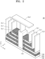
- FIG. 2 is a perspective view illustrating a semiconductor apparatus 20 according to an embodiment.
- a selection device layer 130 and a phase change material layer 110 may be arranged side by side on an X-Y plane to form a semiconductor unit device and such semiconductor unit devices may be arranged while being separated from each other by first insulating layers 200 in a direction (Z direction) perpendicular to a substrate 100.
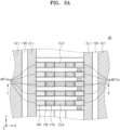
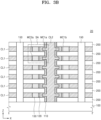
- FIG. 3A is a plan view illustrating a semiconductor apparatus 20 according to an embodiment
- FIG. 3B is a cross-sectional view taken along line I-I' of FIG. 3A
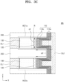
- FIG. 3C is an enlarged view schematically illustrating a region SA of FIG. 3B .
- the semiconductor apparatus 20 may include semiconductor unit devices MC1a, MC1b, and MC2a, wherein the semiconductor unit devices MC1a and MC2a may be apart from each other in a Z direction with a first insulating layer 200 therebetween, the semiconductor unit devices MC1a and MC1b may be apart from each other on an X-Y plane with a second insulating layer 210 therebetween, and each of the semiconductor unit devices MC1a, MC1b, and MC2a may include a selection device layer 130 and a phase change material layer 110, which are arranged in a direction (X direction) parallel to a substrate 100.
- the phase change material layer 110 includes a first chalcogen layer 110a including Ge-Te and a second chalcogen layer 110b including Sb-Te.
- the first chalcogen layer 110a and the second chalcogen layer 110b may form a superlattice-like structure.
- the first chalcogen layer 110a and the second chalcogen layer 110b may be alternately arranged one or more times in a direction (X direction) parallel to the substrate 100.
- the phase change material layer 110 may be expressed as (A m B 1-m ) n .
- A refers to the first chalcogen layer 110a
- B refers to the second chalcogen layer 110b
- n refers to the number of arrangements of the first chalcogen layer 110a and the second chalcogen layer 110b.
- the number (n) of arrangements of the first chalcogen layer 110a and the second chalcogen layer 110b may be 1.5 or more, 2 or more, 2.5 or more, 3 or more, 200 or less, 150 or less, 130 or less, 100 or less, 95 or less, or 90 or less.
- the first chalcogen layer 110a includes a compound represented by Ge x Te 1-x (0.3 ⁇ x ⁇ 0.7), and the second chalcogen layer 110b includes a compound represented by Sb y Te 1-y (0.2 ⁇ y ⁇ 0.8).
- the first chalcogen layer 110a and/or the second chalcogen layer 110b may each independently further include at least one dopant material selected from the group consisting of carbon (C), nitrogen (N), indium (In), zinc (Zn), Scandium (Sc), and tin (Sn).
- the phase change material layer 110 may have a thickness of about 30 nm or more, about 35 nm or more, about 40 nm or more, about 100 nm or less, about 95 nm or less, about 90 nm or less, about 85 nm or less, or about 80 nm or less in the direction (X direction) parallel to the substrate 100.
- the first chalcogen layer 110a and the second chalcogen layer 110b may each independently have a thickness of about 1 nm or more, about 2 nm or more, about 3 nm or more, about 5 nm or more, about 20 nm or less, about 15 nm or less, or about 10 nm or less.
- first chalcogen layer 110a and/or the second chalcogen layer 110b may each have an electron carrier path therein. Therefore, because the semiconductor unit devices MC1a and MC2a arranged adjacent to each other in a vertical direction (Z direction) share the first chalcogen layer 110a and/or the second chalcogen layer 110b, cross-talk may occur between the semiconductor unit devices MC1a and MC2a.
- the semiconductor apparatus 20 is configured such that transfer of electrons in the phase change material layer 110 between the semiconductor unit devices MC1a and MC2a adjacent to each other may be minimized or prevented (and/or limited).
- each selection device layers 130 may be arranged between two first insulating layers 200 to form a recess portion R while covering portions of surfaces of the two first insulating layers 200, and the phase change material layer 110 may be arranged along the recess portion R to cover the two first insulating layers 200 and the selection device layer 130.
- the length d2 of a surface of the phase change material layer 110, which is adjacent to each first insulating layer 200, may be equal to or greater than the length d1 of a surface of the phase change material layer 110, which is adjacent to each selection device layer 130, and thus cross-talk between the semiconductor unit devices MC1a and MC2a adjacent to each other may be minimized.
- the length d2 of the surface of the phase change material layer 110, which is adjacent to each first insulating layer 200, may be greater than the length d1 of the surface of the phase change material layer 110, which is adjacent to each selection device layer 130 by a factor of greater than about 1.0 or more, or by a factor of about 1.5 or more, about 2.0 or more, about 5.0 or less, about 4.5 or less, or about 4.0 or less.
- first and second chalcogen layers may be electrically insulated by a first insulating layer.
- FIG. 4 illustrates a semiconductor apparatus 30 according to another embodiment.
- the semiconductor apparatus 30 may include: a first semiconductor unit device MC1a including a first selection device layer 1301 and a first phase change material layer 1101, which extend side by side in a direction parallel to a substrate 100; and a second semiconductor unit device MC2a including a second selection device layer 1302 and a second phase change material layer 1102, which extend side by side in the direction parallel to the substrate 100, wherein the first semiconductor unit device MC1a and the second semiconductor unit device MC2a may be apart from each other with a first insulating layer 200 therebetween in a direction normal to the substrate 100.
- the first phase change material layer 1101 and the second phase change material layer 1102 may include first chalcogen layers 1101a and 1102a and second chalcogen layers 1101b and 1102b, which extend in the direction parallel to the substrate 100.
- the first phase change material layer 1101 and the second phase change material layer 1102 are physically separated from each other and are electrically insulated from each other by the first insulating layer 200 such that transfer of electrons between the first and second semiconductor unit devices MC1a and MC2a may be prevented.
- the thickness of the first insulating layer 200 may be about 5 nm or more, about 10 nm or more, about 15 nm or more, about 50 nm or less, about 45 nm or less, about 40 nm or less, about 35 nm or less, or about 30 nm or less.
- the selection device layer 130 may include a material of which the resistance is variable according to the magnitude of voltage applied between both ends of the selection device layer 130.
- the selection device layer 130 may include a p-n junction, or may include a mixed ion-electron conductor (MIEC) or a Mott transition device.
- the selection device layer 130 may include a diode.
- the diode may have a junction structure (not shown) in which materials having different conductivity types extend side by side in a direction parallel to the substrate 100.
- the diode may have an N-type and a P-type as conductivity types, wherein one of the N-type and P-type may be arranged adjacent to a first electrode CL1, and the other of the N-type and P-type may be arranged adjacent to the phase change material layer 110 and/or a second electrode CL2.
- the selection device layer 130 may include a silicon diode in which P-Si and N-Si are bonded to each other.
- the selection device layer 130 may include an oxide diode in which P-NiO x and N-TiO x are bonded to each other or P-CuO x and N-TiO x are bonded to each other.
- the selection device layer 130 may have ovonic threshold Switching (OTS) characteristics.
- OTS ovonic threshold Switching
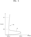
- FIG. 5 is a graph schematically illustrating a voltage-current curve of the selection device layer 130 having ovonic threshold switching characteristics.
- a first curve 61 shows a voltage-current relationship in a state in which little current flows through the selection device layer 130. While voltage gradually increases from a state in which voltage and current are zero, the selection device layer 130 may stay in a high resistance state in which little current flows until the voltage reaches a threshold voltage V T (first voltage level 63). However, as soon as the voltage exceeds the threshold voltage VT, the selection device layer 130 may enter into a low resistance state in which current flowing through the selection device layer 130 increases rapidly, and the voltage applied to the selection device layer 130 may decrease to a saturation voltage V S (second voltage level 64).
- a second curve 62 shows a voltage-current relationship in a state in which current flows smoothly through the selection device layer 130.
- the voltage applied to the selection device layer 130 may slightly increase from the second voltage level 64.
- the voltage applied to the selection device layer 130 may slightly increase from the second voltage level 64.
- the voltage applied to the selection device layer 130 may be maintained at a level substantially equal to the saturation voltage V S .
- the selection device layer 130 When the current decreases below a holding current level (first current level 66), the selection device layer 130 returns to the high resistance state such that current may be effectively blocked until the voltage increases again to the threshold voltage V T . Owing to this, the selection device layer 130 may have switching characteristics with a threshold voltage V T at the first voltage level 63.
- the selection device layer 130 having ovonic threshold switching characteristics may include: a first element including germanium (Ge) and/or tin (Sn); a second element including arsenic (As), antimony (Sb), and/or bismuth (Bi); and a third element including sulfur (S), selenium (Se), and/or tellurium (Te)
- the selection device layer 130 may include the first element in an amount of about 5.0 at% to about 30.0 at% based on a total element amount.
- the selection device layer 130 may include the first element in an amount of about 7.0 at% or more, about 10.0 at% or more, about 25.0 at% or less, about 23.0 at% or less, or about 20.0 at% or less based on a total element amount.
- the selection device layer 130 may include the second element in an amount of about 5.0 at% to about 50.0 at% based on a total element amount.
- the selection device layer 130 may include the second element in an amount of about 7.0 at% or more, about 10.0 at% or more, about 15.0 at% or more, about 20.0 at% or more, about 45.0 at% or less, about 40.0 at% or less, or about 35.0 at% or less based on a total element amount.
- the selection device layer 130 may include the third element in an amount of greater than about 0.0 at% to about 70.0 at% based on a total element amount.
- the selection device layer 130 may include the third element in an amount of about 10.0 at% or more, about 15 at% or more, about 20.0 at% or more, about 25.0 at% or more, about 30.0 at% or more, about 35.0 at% or more, about 40.0 at% or more, about 65.0 at% or less, about 60.0 at% or less, or about 55.0 at% or less based on a total element amount.
- the selection device layer 130 and the phase change material layer 110 may be electrically connected to each other.
- a third electrode 120 may be further included between the selection device layer 130 and the phase change material layer 110.
- the third electrode 120 may include a metal, a conductive metal nitride, a conductive metal oxide, or a combination thereof.
- the third electrode 120 may include at least one selected from the group consisting of carbon (C), titanium nitride (TiN), titanium silicon nitride (TiSiN), titanium carbon nitride (TiCN), titanium carbon silicon nitride (TiCSiN), titanium aluminum nitride (TiAlN), tantalum (Ta), tantalum nitride (TaN), tungsten (W), and tungsten nitride (WN).
- C carbon
- TiN titanium nitride
- TiSiN titanium silicon nitride
- TiCN titanium carbon nitride
- TiCSiN titanium aluminum nitride
- Ta tantalum
- TaN tantalum nitride
- W tungsten
- WN tungsten nitride
- a heating electrode (not shown) may be further included between the third electrode 120 and the phase change material layer 110.
- the heating electrode and the third electrode 120 may be formed in one piece or as separate layers.
- the heating electrode may include a conductive material capable of generating sufficient heat to change the phase of the phase change material layer 110 without reacting with the phase change material layer 110.
- the heating electrode may include a carbon-based conductive material.
- the heating electrode may include TiN, TiSiN, TiAlN, TaSiN, TaAlN, TaN, WSi, WN, TiW, MoN, NbN, TiBN, ZrSiN, WSiN, WBN, ZrAIN, MoAlN, TiAl, TiON, TiAlON, WON, TaON, carbon (C), silicon carbide (SiC), silicon carbon nitride (SiCN), carbon nitride (CN), titanium carbon nitride (TiCN), tantalum carbon nitride (TaCN), or a combination thereof.
- the third electrode 120 may have a thickness such that heat generated by the heating electrode (not shown) may not substantially affect the selection device layer 130.
- the third electrode 120 may further include a thermal barrier layer, and may have a structure in which the thermal barrier layer and an electrode material layer are alternately stacked.
- the third electrode 120 may have a thickness of about 10 nm to about 100 nm.
- the first electrode CL1 and the second electrode CL2 may be arranged on both ends of the semiconductor unit devices MC1a and MC2a.
- the first electrode CL1 may be electrically connected to the selection device layer 130
- the second electrode CL2 may be electrically connected to the phase change material layer 110.
- First electrodes CL1 may extend parallel to each other in the X direction, and each of the first electrodes CL1 may be arranged between two first insulating layers 200.
- second electrodes CL2 may extend parallel to each other in the Z direction, and each of the second electrodes CL2 may be arranged between two second insulating layers 210.
- the first electrode CL1 may be connected to one of a word line and a bit line, and the second electrode CL2 may be connected to the other.
- One or both of the first electrode CL1 and the second electrode CL2 may each be a common electrode of the semiconductor unit devices MC1a, MC1b, and MC2a. For example, referring to FIGS.
- the first electrodes CL1 may extend in the Y direction between the first insulating layers 200, which are apart from each other in the Z direction, and each of the first electrodes CL1 may be commonly connected to a plurality of semiconductor unit devices MC1a or MC1b arranged at the same level.
- the second electrodes CL2 may extend in the Z direction between the second insulating layers 210, which are apart from each other in the Y direction, and each of the second electrodes CL2 may be commonly connected to a plurality of semiconductor unit devices MC1a, MC1b, and MC2a arranged at the same level.
- the substrate 100 may include a semiconductor material such as silicon (Si), germanium (Ge), silicon germanium (SiGe), silicon carbide (SiC), gallium arsenide (GaAs), indium arsenide (InAs), or indium phosphide (InP), and the substrate 100 may include an insulating material such as silicon oxide, silicon nitride, or silicon oxynitride.
- a semiconductor material such as silicon (Si), germanium (Ge), silicon germanium (SiGe), silicon carbide (SiC), gallium arsenide (GaAs), indium arsenide (InAs), or indium phosphide (InP)
- the substrate 100 may include an insulating material such as silicon oxide, silicon nitride, or silicon oxynitride.
- Each of the semiconductor apparatuses 20 and 30 may further include an interlayer insulating layer (not shown) on the substrate 100.
- the interlayer insulating layer (not shown) may be arranged between the substrate 100 and the first electrode CL1 and/or the second electrode CL2 to electrically separate the substrate 100 from the first electrode CL1 and/or the second electrode CL2.
- the interlayer insulating layer (not shown) may include an oxide such as silicon oxide and/or a nitride such as silicon nitride.
- Each of the semiconductor apparatuses 20 and 30 may further include an isolation insulating layer 150.
- the isolation insulating layer 150 may be in contact with an upper surface of the substrate 100 and may extend in the Z direction from the upper surface of the substrate 100.
- the isolation insulating layer 150 may be formed through the first electrodes CL1 and the first insulating layers 200.
- isolation insulating layers 150 may extend along sides of the first electrodes CL1 or in the Y direction at both sides of each of the second insulating layers 210, or each of the isolation insulating layers 150 may be arranged between two first electrodes CL1, which are adjacent to each other in the X direction.
- Each of the semiconductor apparatuses 20 and 30 may further include a driving circuit region (not shown) on the substrate 100.
- the driving circuit region may include circuit units such as a peripheral circuit, a driving circuit, and a core circuit configured to drive the semiconductor unit devices or perform arithmetic processing.
- the circuits may include, for example, a page buffer, a latch circuit, a cache circuit, a column decoder, a sense amplifier, a data in/out circuit, or a row decoder.
- the circuits may be arranged between the substrate 100 and the semiconductor unit devices.
- the driving circuit region and the semiconductor unit devices may be sequentially arranged on the substrate 100, and this arrangement structure may be a cell-on-peri (COP) structure.
- COP cell-on-peri
- the driving circuit region may include one or more transistors and wiring structures, which are electrically connected to the transistors.
- the transistors may be arranged in active regions of the substrate 100, which are defined by a device isolation layer.
- Each of the transistors may include a gate, a gate insulating layer, and a source/drain.
- insulating spacers may be arranged on both sidewalls of the gate, and an etch stop layer may be arranged on the gate and/or the insulating spacers.
- the etch stop layer may include an insulating material such as silicon nitride or silicon oxynitride.
- the number and positions of wiring structures may be determined according to the layout of the driving circuit region and the type and arrangement of the gates.
- the wiring structures may have a multilayer structure having two or more layers.
- each of the wiring structures may include a contact and a wiring layer, which are electrically connected to each other and are sequentially stacked on the substrate 100.
- the contact and the wiring layer may each independently include a metal, a conductive metal nitride, a metal silicide, or a combination thereof, and may include a conductive material such as tungsten, molybdenum, titanium, cobalt, tantalum, nickel, tungsten silicide, titanium silicide, cobalt silicide, tantalum silicide, or nickel silicide.
- the wiring structures may include interlayer insulating layers, which electrically separate components from each other.
- the interlayer insulating layers may be arranged between a plurality of transistors, between a plurality of wiring layers, and/or between a plurality of contacts.
- the interlayer insulating layers may include silicon oxide, silicon nitride, silicon oxynitride, or the like.
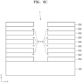
- FIGS. 6A to 6G are cross-sectional views illustrating some processes of manufacturing a semiconductor apparatus according to an embodiment.
- a structure L is formed by alternately stacking a first insulating layer 200 and a sacrificial layer 300 on a substrate 100.
- first insulating layers 200 may be arranged on a surface of the substrate 100 and the uppermost portion of the structure L.
- a vertical trench T is formed through the structure L in the Z direction.
- sub-structures L1 and L2 may be formed on both sides of the vertical trench T.
- sacrificial layers 300 are selectively removed to form a horizontal hole H between every two first insulating layers 200 in an X direction.
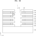
- selection device layers 130 are formed in portions of the horizontal holes H. Each of the selection device layers 130 may form a first recess portion R1 together with two first insulating layers 200.
- third electrodes 120 are formed in the remaining portions of the horizontal holes H.
- Each of the third electrodes 120 may extend in a direction parallel to the selection device layers 130 and the substrate 100 and may form a second recess portion R2 together with two first insulating layers 200.
- the length d2 of a portion of each of the first insulating layers 200, which is exposed in the vertical trench T and horizontal holes H may be greater than the length d1 of each of the second recesses R2 between two first insulating layers 200.
- the length d2 of the portion of the first insulating layer 200 exposed in the vertical trench T and the horizontal holes H may be greater than the length d1 between two first insulating layers 200 by a factor of greater than about 1.0 or more, or by a factor of about 1.5 or more, about 2.0 or more, about 5.0 or less, about 4.5 or less, or about 4.0 or less.
- a phase change material layer 110 is formed along sidewalls of the horizontal holes H and the vertical trench T.
- the phase change material layer 110 may be formed by alternately stacking a first chalcogen layer 110a and a second chalcogen layer 110b.
- a second electrode CL2 is formed in the remaining portions of the horizontal holes H and the trench T.
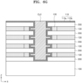
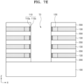
- processes illustrated in FIGS. 7A to 7E may be added between the processes illustrated in FIGS. 6F and 6G for the embodiment illustrated in FIG. 4 .
- the sacrificial layer SL, the first insulating layers 200, and the phase change material layer 110 may be partially removed (etched) until a length at which most of the phase change material layer 110 covering the first insulating layer 200 is removed (refer to FIG. 7B ).
- FIG. 7B After selectively removing portions of the phase change material layer 110 that are not covered by the remaining portion of the sacrificial layer SL between every two first insulating layers 200 (refer to FIG.
- the phase change material layer 110 may be further formed at positions of the removed portions of the phase change material layer 110 up to the height of the remaining phase change material layer 110 (up to a height below which the phase change material layer 110 does not make contact with the sacrificial layer SL) (refer to FIG. 7D ). Thereafter, the remaining portion of the sacrificial layer SL may be removed, and a trench T2, which is wider than the trench T shown in FIG. 6F , may be formed (refer to FIG. 7E ). The trench T2 may be filled with a material of the second electrode CL2 as shown in FIG. 6G .
- components such as the first and second electrodes CL1 and CL2, the first and second insulating layers 200 and 210, the selection device layers 130, the third electrodes 120, and the phase change material layer 110 may be formed by methods known in the art.
- Each of the components may be independently formed to have an intended composition and thickness through a deposition method such as atomic layer deposition (ALD), chemical vapor deposition (CVD), physical vapor deposition (PVD), or sputtering.
- the phase change material layer 110 may be formed by an ALD method in which sources of germanium (Ge), tellurium (Te), antimony (Sb), and tellurium (Te) are sequentially used.
- the components may be independently patterned by methods known in the art.
- a damascene method may also be used in addition to an embossing etching method in which a mask pattern is used.
- FIG. 8 is diagram of an electronic device including a semiconductor apparatus according to an example embodiment.
- an electronic device 1000 may include a controller 500, a memory controller 550, a display device 600 (e.g., OLED display, holographic display), and a semiconductor apparatus 101, which may be connected to each other through a bus (not shown).
- the memory controller 550 may include a read/write circuit 560 and a word line driver circuit 570.
- the read/write circuit 560 and word line driver circuit 570 may be electrically connected to the semiconductor apparatus 101 through first electrode lines (e.g., WL1) and second line lines (e.g., BL1).
- the controller 500 may control operations of the electronic system 1000 and may include processing circuitry 510, a host interface 515, and a power management circuit 520.
- the semiconductor apparatus 101 may be implemented using one of the semiconductor apparatuses 101, 20, and 30 described above.
- the processing circuitry 510 may operate in response to those commands and may control operations of the display device 600, memory controller 550, and/or semiconductor apparatus 101.
- the controller 500 may control the display device 600 by providing commands and information to the display device 600 and by controlling power to the display device 600 using the power management circuit 520.
- the controller 500 may control power provided to the memory controller 550 and semiconductor apparatus 101 using the power management circuit 520.
- the controller 500 may control operations of the semiconductor apparatus 101 by providing commands to the memory controller 550.
- the controller 500 may also provide the memory controller 550 with data to be written in the semiconductor apparatus 101 and/or may receive data read from the semiconductor apparatus 101.
- the memory controller 550 in response to receiving commands from the controller 500 and/or in response to receiving data for a write operation, may control the semiconductor apparatus 101 using the read/write circuit 560 and word line driver circuit 570 to write data, read data, and/or erase data in one or more selected semiconductor unit devices MC of the semiconductor apparatus 101.
- the memory controller 550 in response to receiving commands from the controller 500, may read data from the semiconductor apparatus 101 and provide the data read from the semiconductor apparatus 101 to the controller 500.
- semiconductor apparatuses each including a plurality of semiconductor unit devices may be provided.
- Semiconductor apparatuses each including a phase change material layer having a superlattice-like structure may be provided.
- the semiconductor apparatuses may be driven with low power and may have a high degree of integration such that the semiconductor apparatuses may contribute to miniaturization of electronic apparatuses.
- the semiconductor apparatuses may be implemented in electronic devices using the semiconductor apparatuses.
- processing circuitry such as hardware including logic circuits; a hardware/software combination such as a processor executing software; or a combination thereof.
- the processing circuitry more specifically may include, but is not limited to, a central processing unit (CPU), an arithmetic logic unit (ALU), a digital signal processor, a microcomputer, a field programmable gate array (FPGA), a System-on-Chip (SoC), a programmable logic unit, a microprocessor, application-specific integrated circuit (ASIC), etc.
- CPU central processing unit
- ALU arithmetic logic unit
- FPGA field programmable gate array
- SoC System-on-Chip
- ASIC application-specific integrated circuit
Landscapes
- Engineering & Computer Science (AREA)
- Manufacturing & Machinery (AREA)
- Chemical & Material Sciences (AREA)
- Crystallography & Structural Chemistry (AREA)
- Semiconductor Memories (AREA)
Claims (13)
- Halbleiterbauelement (20), umfassend:ein Substrat (100);eine erste Isolierschicht (200) und eine zweite Isolierschicht (210), die voneinander in einer Richtung normal zu dem Substrat getrennt sind; undeine Halbleitereinheitsvorrichtung (20) zwischen der ersten Isolierschicht und der zweiten Isolierschicht, wobeidie Halbleitereinheitsvorrichtung (MC 1a, MC1b, MC1c) eine Auswahlvorrichtungsschicht (130) und eine Phasenwechselmaterialschicht (110) einschließt, die sich Seite an Seite in einer Richtung parallel zu dem Substrat erstrecken,die Phasenwechselmaterialschicht eine erste Chalkogenschicht einschließt, die GexTe1-x einschließt, wobei 0,3≤x≤0,7,und eine zweite Chalkogenschicht, die SbyTe1-y einschließt, wobei 0,2≤y≤0,8,die Auswahlvorrichtungsschicht (130) einen Vertiefungsabschnitt (R) bildet, indem sie einen Abschnitt einer Oberfläche der ersten Isolierschicht und einen Abschnitt einer Oberfläche der zweiten Isolierschicht derart bedeckt, dass eine Seitenwand der Auswahlvorrichtungsschicht relativ zu einer Seitenwand der ersten Isolierschicht und einer Seitenwand der zweiten Isolierschicht vertieft ist,die Phasenwechselmaterialschicht entlang des Vertiefungsabschnitts angeordnet ist, um die erste Isolierschicht, die Auswahlvorrichtungsschicht und die zweite Isolierschicht zu bedecken, undeine Länge einer Oberfläche der Phasenwechselmaterialschicht benachbart zu der ersten Isolierschicht gleich oder größer als eine Länge einer Oberfläche der Phasenwechselmaterialschicht benachbart zu der Auswahlvorrichtungsschicht ist.
- Halbleiterbauelement nach Anspruch 1, wobei die Länge der Oberfläche der Phasenwechselmaterialschicht benachbart zu der ersten Isolierschicht um einen Faktor von mehr als 1,0 bis 5,0 größer als die Länge der Oberfläche der Phasenwechselmaterialschicht benachbart zu der Auswahlvorrichtungsschicht ist.
- Halbleiterbauelement nach Anspruch 1 oder 2, wobei die erste Chalkogenschicht und die zweite Chalkogenschicht eine übergitterartige Struktur bilden.
- Halbleiterbauelement nach einem vorhergehenden Anspruch, wobei die erste Chalkogenschicht und die zweite Chalkogenschicht abwechselnd einmal oder mehrmals in der Richtung parallel zu dem Substrat angeordnet sind.
- Halbleiterbauelement nach einem vorhergehenden Anspruch, wobei die erste Chalkogenschicht und die zweite Chalkogenschicht jeweils unabhängig voneinander eine Dicke von 1 nm bis 20 nm in der Richtung parallel zu dem Substrat aufweisen.
- Halbleiterbauelement nach einem vorhergehenden Anspruch, wobei die erste Chalkogenschicht, die zweite Chalkogenschicht oder sowohl die erste Chalkogenschicht als auch die zweite Chalkogenschicht jeweils unabhängig voneinander mindestens ein Dotierungsmaterial umfassen, das aus der Gruppe ausgewählt ist, die aus Kohlenstoff (C), Stickstoff (N), Indium (In), Zink (Zn), Scandium (Sc) und Zinn (Sn) besteht.
- Halbleiterbauelement nach einem vorhergehenden Anspruch, wobei die Auswahlvorrichtungsschicht und die Phasenwechselmaterialschicht elektrisch miteinander verbunden sind.
- Halbleiterbauelement nach einem vorhergehenden Anspruch, ferner umfassend:
eine Heizelektrodenschicht zwischen der Auswahlvorrichtungsschicht und der Phasenwechselmaterialschicht. - Halbleiterbauelement nach einem vorhergehenden Anspruch, wobei die Phasenwechselmaterialschicht eine Dicke von 30 nm bis 100 nm aufweist.
- Halbleiterbauelement nach einem vorhergehenden Anspruch, ferner umfassend:eine erste Elektrode (CL1),die elektrisch mit der Auswahlvorrichtungsschicht verbunden ist; undeine zweite Elektrode (CL2),die elektrisch mit der Phasenwechselmaterialschicht verbunden ist.
- Halbleiterbauelement nach Anspruch 10, ferner umfassend:eine Vielzahl von Halbleitereinheitsvorrichtungen auf dem Substrat, wobei die Halbleitereinheitsvorrichtung eine der Vielzahl von Halbleitereinheitsvorrichtungen ist unddie Vielzahl von Halbleitereinheitsvorrichtungen die erste Elektrode oder die zweite Elektrode als eine gemeinsame Elektrode umfasst.
- Halbleiterbauelement nach einem vorhergehenden Anspruch, wobei die Auswahlvorrichtungsschicht ein Material mit ovonischen Schwellenwertschalteigenschaften umfasst.
- Halbleiterbauelement nach Anspruch 12, wobei die Auswahlvorrichtungsschicht Folgendes umfasst:mindestens ein erstes Element, das aus der Gruppe ausgewählt ist, die aus Germanium (Ge) und Zinn (Sn) besteht;mindestens ein zweites Element, das aus der Gruppe ausgewählt ist, die aus Arsen (As), Antimon (Sb) und Bismut (Bi) besteht; undmindestens ein drittes Element, das aus der Gruppe ausgewählt ist, die aus Schwefel (S), Selen (Se) und Tellur (Te) besteht.
Applications Claiming Priority (2)
| Application Number | Priority Date | Filing Date | Title |
|---|---|---|---|
| KR20200163333 | 2020-11-27 | ||
| KR1020200188076A KR102866072B1 (ko) | 2020-11-27 | 2020-12-30 | 반도체 장치 |
Publications (2)
| Publication Number | Publication Date |
|---|---|
| EP4007000A1 EP4007000A1 (de) | 2022-06-01 |
| EP4007000B1 true EP4007000B1 (de) | 2023-04-19 |
Family
ID=76764889
Family Applications (1)
| Application Number | Title | Priority Date | Filing Date |
|---|---|---|---|
| EP21183408.0A Active EP4007000B1 (de) | 2020-11-27 | 2021-07-02 | Halbleiterbauelement |
Country Status (4)
| Country | Link |
|---|---|
| US (3) | US11744167B2 (de) |
| EP (1) | EP4007000B1 (de) |
| JP (1) | JP7849103B2 (de) |
| CN (1) | CN114566591A (de) |
Families Citing this family (5)
| Publication number | Priority date | Publication date | Assignee | Title |
|---|---|---|---|---|
| KR102866070B1 (ko) * | 2020-11-10 | 2025-09-26 | 삼성전자주식회사 | 칼코겐 화합물 및 이를 포함하는 반도체 소자 |
| US12004433B2 (en) * | 2022-07-05 | 2024-06-04 | Toshiba Global Commerce Solutions, Inc. | Multi-bit storage device using phase change material |
| TWI862352B (zh) * | 2023-01-04 | 2024-11-11 | 力晶積成電子製造股份有限公司 | 三維相變化記憶體及其製作方法 |
| US20240276893A1 (en) * | 2023-02-14 | 2024-08-15 | Taiwan Semiconductor Manufacturing Company Limited | Phase change material switch with ovonic threshold switching material selector and methods for forming the same |
| US20240357948A1 (en) * | 2023-04-18 | 2024-10-24 | Taiwan Semiconductor Manufacturing Company, Ltd. | Semiconductor device with phase-change material and method for manufacturing thereof |
Citations (1)
| Publication number | Priority date | Publication date | Assignee | Title |
|---|---|---|---|---|
| US20200105835A1 (en) * | 2018-09-28 | 2020-04-02 | Intel Corporation | 3d memory array with memory cells having a 3d selector and a storage component |
Family Cites Families (20)
| Publication number | Priority date | Publication date | Assignee | Title |
|---|---|---|---|---|
| US8030734B2 (en) | 2008-12-30 | 2011-10-04 | Stmicroelectronics S.R.L. | Forming phase change memories with a breakdown layer sandwiched by phase change memory material |
| US8693241B2 (en) | 2011-07-13 | 2014-04-08 | SK Hynix Inc. | Semiconductor intergrated circuit device, method of manufacturing the same, and method of driving the same |
| KR20140068627A (ko) | 2012-11-28 | 2014-06-09 | 삼성전자주식회사 | 가변저항막을 갖는 저항 메모리 소자 및 그 제조방법 |
| JP5957375B2 (ja) | 2012-11-30 | 2016-07-27 | 株式会社日立製作所 | 相変化メモリ |
| JP5826779B2 (ja) | 2013-02-27 | 2015-12-02 | 株式会社東芝 | 不揮発性半導体記憶装置 |
| US9450023B1 (en) | 2015-04-08 | 2016-09-20 | Sandisk Technologies Llc | Vertical bit line non-volatile memory with recessed word lines |
| KR102465967B1 (ko) * | 2016-02-22 | 2022-11-10 | 삼성전자주식회사 | 메모리 소자 및 그 제조방법 |
| JP6697366B2 (ja) * | 2016-10-20 | 2020-05-20 | キオクシア株式会社 | 超格子メモリ及びクロスポイント型メモリ装置 |
| KR102295524B1 (ko) * | 2017-03-27 | 2021-08-30 | 삼성전자 주식회사 | 메모리 소자 |
| JP6505799B2 (ja) | 2017-09-20 | 2019-04-24 | 株式会社東芝 | 記憶装置 |
| KR102119306B1 (ko) | 2018-04-25 | 2020-06-04 | 서울과학기술대학교 산학협력단 | 저항 스위칭 소자 및 이를 이용한 상변화 메모리 소자 |
| US10381559B1 (en) * | 2018-06-07 | 2019-08-13 | Sandisk Technologies Llc | Three-dimensional phase change memory array including discrete middle electrodes and methods of making the same |
| KR102546686B1 (ko) * | 2018-07-17 | 2023-06-23 | 삼성전자주식회사 | 가변 저항 메모리 장치 |
| KR102578801B1 (ko) * | 2018-08-29 | 2023-09-18 | 삼성전자주식회사 | 가변 저항 메모리 장치 |
| JP2020047316A (ja) | 2018-09-14 | 2020-03-26 | キオクシア株式会社 | 不揮発性記憶装置 |
| KR102649489B1 (ko) | 2019-01-11 | 2024-03-21 | 삼성전자주식회사 | 가변 저항 메모리 소자 |
| US11282895B2 (en) * | 2019-07-02 | 2022-03-22 | Micron Technology, Inc. | Split pillar architectures for memory devices |
| CN110571235A (zh) | 2019-08-30 | 2019-12-13 | 华中科技大学 | 一种三维超晶格相变存储阵列及其制备方法与应用 |
| KR102702798B1 (ko) * | 2019-12-26 | 2024-09-05 | 에스케이하이닉스 주식회사 | 전자 장치 및 전자 장치의 제조 방법 |
| US20220093861A1 (en) * | 2020-09-22 | 2022-03-24 | Asm Ip Holding B.V. | Systems, devices, and methods for depositing a layer comprising a germanium chalcogenide |
-
2021
- 2021-05-26 US US17/330,950 patent/US11744167B2/en active Active
- 2021-07-02 EP EP21183408.0A patent/EP4007000B1/de active Active
- 2021-08-16 CN CN202110935795.5A patent/CN114566591A/zh active Pending
- 2021-11-26 JP JP2021192096A patent/JP7849103B2/ja active Active
-
2023
- 2023-07-10 US US18/349,433 patent/US12268105B2/en active Active
-
2024
- 2024-12-13 US US18/980,759 patent/US20250113746A1/en active Pending
Patent Citations (1)
| Publication number | Priority date | Publication date | Assignee | Title |
|---|---|---|---|---|
| US20200105835A1 (en) * | 2018-09-28 | 2020-04-02 | Intel Corporation | 3d memory array with memory cells having a 3d selector and a storage component |
Also Published As
| Publication number | Publication date |
|---|---|
| US11744167B2 (en) | 2023-08-29 |
| JP7849103B2 (ja) | 2026-04-21 |
| US12268105B2 (en) | 2025-04-01 |
| US20220173316A1 (en) | 2022-06-02 |
| EP4007000A1 (de) | 2022-06-01 |
| JP2022085888A (ja) | 2022-06-08 |
| US20250113746A1 (en) | 2025-04-03 |
| CN114566591A (zh) | 2022-05-31 |
| US20230354725A1 (en) | 2023-11-02 |
Similar Documents
| Publication | Publication Date | Title |
|---|---|---|
| EP4007000B1 (de) | Halbleiterbauelement | |
| CN107104122B (zh) | 存储器件 | |
| US10186552B2 (en) | Variable resistance memory device and method of manufacturing the same | |
| CN107644934B (zh) | 存储器件 | |
| US9741764B1 (en) | Memory device including ovonic threshold switch adjusting threshold voltage thereof | |
| US9887354B2 (en) | Memory device and method of manufacturing the same | |
| US9941333B2 (en) | Memory device and method of manufacturing the same | |
| US20170244026A1 (en) | Variable resistance memory device and method of manufacturing the same | |
| US20180277601A1 (en) | Memory device including a variable resistance material layer | |
| US9608041B2 (en) | Semiconductor memory device and method of manufacturing the same | |
| KR20170098673A (ko) | 메모리 소자 | |
| US12414309B2 (en) | Memory device including phase-change material | |
| US20230240086A1 (en) | Semiconductor memory device and manufacturing method thereof | |
| KR102866072B1 (ko) | 반도체 장치 | |
| KR102778966B1 (ko) | 가변 저항 메모리 소자 및 그 제조 방법 | |
| KR102792396B1 (ko) | 가변 저항 메모리 소자 및 그 제조 방법 | |
| KR102666706B1 (ko) | 가변 저항 메모리 소자 및 그 제조 방법 | |
| US20230403955A1 (en) | Semiconductor memory device | |
| US11581485B2 (en) | Semiconductor memory device and method for manufacturing semiconductor memory device | |
| KR20250112591A (ko) | 가변 저항 메모리 소자 및 그 제조 방법 | |
| KR20250112595A (ko) | 가변 저항 메모리 소자 및 그 제조 방법 | |
| KR20250112592A (ko) | 가변 저항 메모리 소자 및 그 제조 방법 | |
| KR20250020085A (ko) | 가변 저항 메모리 소자 | |
| US20090225580A1 (en) | Integrated Circuit, Memory Module, and Method of Manufacturing an Integrated Circuit | |
| KR20250113180A (ko) | 가변 저항 메모리 소자 |
Legal Events
| Date | Code | Title | Description |
|---|---|---|---|
| PUAI | Public reference made under article 153(3) epc to a published international application that has entered the european phase |
Free format text: ORIGINAL CODE: 0009012 |
|
| STAA | Information on the status of an ep patent application or granted ep patent |
Free format text: STATUS: REQUEST FOR EXAMINATION WAS MADE |
|
| 17P | Request for examination filed |
Effective date: 20220331 |
|
| AK | Designated contracting states |
Kind code of ref document: A1 Designated state(s): AL AT BE BG CH CY CZ DE DK EE ES FI FR GB GR HR HU IE IS IT LI LT LU LV MC MK MT NL NO PL PT RO RS SE SI SK SM TR |
|
| GRAP | Despatch of communication of intention to grant a patent |
Free format text: ORIGINAL CODE: EPIDOSNIGR1 |
|
| STAA | Information on the status of an ep patent application or granted ep patent |
Free format text: STATUS: GRANT OF PATENT IS INTENDED |
|
| INTG | Intention to grant announced |
Effective date: 20221124 |
|
| GRAS | Grant fee paid |
Free format text: ORIGINAL CODE: EPIDOSNIGR3 |
|
| GRAA | (expected) grant |
Free format text: ORIGINAL CODE: 0009210 |
|
| STAA | Information on the status of an ep patent application or granted ep patent |
Free format text: STATUS: THE PATENT HAS BEEN GRANTED |
|
| AK | Designated contracting states |
Kind code of ref document: B1 Designated state(s): AL AT BE BG CH CY CZ DE DK EE ES FI FR GB GR HR HU IE IS IT LI LT LU LV MC MK MT NL NO PL PT RO RS SE SI SK SM TR |
|
| REG | Reference to a national code |
Ref country code: GB Ref legal event code: FG4D |
|
| REG | Reference to a national code |
Ref country code: DE Ref legal event code: R096 Ref document number: 602021001949 Country of ref document: DE |
|
| REG | Reference to a national code |
Ref country code: CH Ref legal event code: EP |
|
| REG | Reference to a national code |
Ref country code: IE Ref legal event code: FG4D |
|
| REG | Reference to a national code |
Ref country code: AT Ref legal event code: REF Ref document number: 1561855 Country of ref document: AT Kind code of ref document: T Effective date: 20230515 |
|
| P01 | Opt-out of the competence of the unified patent court (upc) registered |
Effective date: 20230520 |
|
| REG | Reference to a national code |
Ref country code: LT Ref legal event code: MG9D |
|
| REG | Reference to a national code |
Ref country code: NL Ref legal event code: MP Effective date: 20230419 |
|
| REG | Reference to a national code |
Ref country code: AT Ref legal event code: MK05 Ref document number: 1561855 Country of ref document: AT Kind code of ref document: T Effective date: 20230419 |
|
| PG25 | Lapsed in a contracting state [announced via postgrant information from national office to epo] |
Ref country code: NL Free format text: LAPSE BECAUSE OF FAILURE TO SUBMIT A TRANSLATION OF THE DESCRIPTION OR TO PAY THE FEE WITHIN THE PRESCRIBED TIME-LIMIT Effective date: 20230419 |
|
| PG25 | Lapsed in a contracting state [announced via postgrant information from national office to epo] |
Ref country code: SE Free format text: LAPSE BECAUSE OF FAILURE TO SUBMIT A TRANSLATION OF THE DESCRIPTION OR TO PAY THE FEE WITHIN THE PRESCRIBED TIME-LIMIT Effective date: 20230419 Ref country code: PT Free format text: LAPSE BECAUSE OF FAILURE TO SUBMIT A TRANSLATION OF THE DESCRIPTION OR TO PAY THE FEE WITHIN THE PRESCRIBED TIME-LIMIT Effective date: 20230821 Ref country code: NO Free format text: LAPSE BECAUSE OF FAILURE TO SUBMIT A TRANSLATION OF THE DESCRIPTION OR TO PAY THE FEE WITHIN THE PRESCRIBED TIME-LIMIT Effective date: 20230719 Ref country code: ES Free format text: LAPSE BECAUSE OF FAILURE TO SUBMIT A TRANSLATION OF THE DESCRIPTION OR TO PAY THE FEE WITHIN THE PRESCRIBED TIME-LIMIT Effective date: 20230419 Ref country code: AT Free format text: LAPSE BECAUSE OF FAILURE TO SUBMIT A TRANSLATION OF THE DESCRIPTION OR TO PAY THE FEE WITHIN THE PRESCRIBED TIME-LIMIT Effective date: 20230419 |
|
| PG25 | Lapsed in a contracting state [announced via postgrant information from national office to epo] |
Ref country code: RS Free format text: LAPSE BECAUSE OF FAILURE TO SUBMIT A TRANSLATION OF THE DESCRIPTION OR TO PAY THE FEE WITHIN THE PRESCRIBED TIME-LIMIT Effective date: 20230419 Ref country code: PL Free format text: LAPSE BECAUSE OF FAILURE TO SUBMIT A TRANSLATION OF THE DESCRIPTION OR TO PAY THE FEE WITHIN THE PRESCRIBED TIME-LIMIT Effective date: 20230419 Ref country code: LV Free format text: LAPSE BECAUSE OF FAILURE TO SUBMIT A TRANSLATION OF THE DESCRIPTION OR TO PAY THE FEE WITHIN THE PRESCRIBED TIME-LIMIT Effective date: 20230419 Ref country code: LT Free format text: LAPSE BECAUSE OF FAILURE TO SUBMIT A TRANSLATION OF THE DESCRIPTION OR TO PAY THE FEE WITHIN THE PRESCRIBED TIME-LIMIT Effective date: 20230419 Ref country code: IS Free format text: LAPSE BECAUSE OF FAILURE TO SUBMIT A TRANSLATION OF THE DESCRIPTION OR TO PAY THE FEE WITHIN THE PRESCRIBED TIME-LIMIT Effective date: 20230819 Ref country code: HR Free format text: LAPSE BECAUSE OF FAILURE TO SUBMIT A TRANSLATION OF THE DESCRIPTION OR TO PAY THE FEE WITHIN THE PRESCRIBED TIME-LIMIT Effective date: 20230419 Ref country code: GR Free format text: LAPSE BECAUSE OF FAILURE TO SUBMIT A TRANSLATION OF THE DESCRIPTION OR TO PAY THE FEE WITHIN THE PRESCRIBED TIME-LIMIT Effective date: 20230720 Ref country code: AL Free format text: LAPSE BECAUSE OF FAILURE TO SUBMIT A TRANSLATION OF THE DESCRIPTION OR TO PAY THE FEE WITHIN THE PRESCRIBED TIME-LIMIT Effective date: 20230419 |
|
| PG25 | Lapsed in a contracting state [announced via postgrant information from national office to epo] |
Ref country code: FI Free format text: LAPSE BECAUSE OF FAILURE TO SUBMIT A TRANSLATION OF THE DESCRIPTION OR TO PAY THE FEE WITHIN THE PRESCRIBED TIME-LIMIT Effective date: 20230419 |
|
| PG25 | Lapsed in a contracting state [announced via postgrant information from national office to epo] |
Ref country code: SK Free format text: LAPSE BECAUSE OF FAILURE TO SUBMIT A TRANSLATION OF THE DESCRIPTION OR TO PAY THE FEE WITHIN THE PRESCRIBED TIME-LIMIT Effective date: 20230419 |
|
| REG | Reference to a national code |
Ref country code: DE Ref legal event code: R097 Ref document number: 602021001949 Country of ref document: DE |
|
| PG25 | Lapsed in a contracting state [announced via postgrant information from national office to epo] |
Ref country code: SM Free format text: LAPSE BECAUSE OF FAILURE TO SUBMIT A TRANSLATION OF THE DESCRIPTION OR TO PAY THE FEE WITHIN THE PRESCRIBED TIME-LIMIT Effective date: 20230419 Ref country code: SK Free format text: LAPSE BECAUSE OF FAILURE TO SUBMIT A TRANSLATION OF THE DESCRIPTION OR TO PAY THE FEE WITHIN THE PRESCRIBED TIME-LIMIT Effective date: 20230419 Ref country code: RO Free format text: LAPSE BECAUSE OF FAILURE TO SUBMIT A TRANSLATION OF THE DESCRIPTION OR TO PAY THE FEE WITHIN THE PRESCRIBED TIME-LIMIT Effective date: 20230419 Ref country code: EE Free format text: LAPSE BECAUSE OF FAILURE TO SUBMIT A TRANSLATION OF THE DESCRIPTION OR TO PAY THE FEE WITHIN THE PRESCRIBED TIME-LIMIT Effective date: 20230419 Ref country code: DK Free format text: LAPSE BECAUSE OF FAILURE TO SUBMIT A TRANSLATION OF THE DESCRIPTION OR TO PAY THE FEE WITHIN THE PRESCRIBED TIME-LIMIT Effective date: 20230419 Ref country code: CZ Free format text: LAPSE BECAUSE OF FAILURE TO SUBMIT A TRANSLATION OF THE DESCRIPTION OR TO PAY THE FEE WITHIN THE PRESCRIBED TIME-LIMIT Effective date: 20230419 |
|
| PLBE | No opposition filed within time limit |
Free format text: ORIGINAL CODE: 0009261 |
|
| STAA | Information on the status of an ep patent application or granted ep patent |
Free format text: STATUS: NO OPPOSITION FILED WITHIN TIME LIMIT |
|
| PG25 | Lapsed in a contracting state [announced via postgrant information from national office to epo] |
Ref country code: MC Free format text: LAPSE BECAUSE OF FAILURE TO SUBMIT A TRANSLATION OF THE DESCRIPTION OR TO PAY THE FEE WITHIN THE PRESCRIBED TIME-LIMIT Effective date: 20230419 |
|
| PG25 | Lapsed in a contracting state [announced via postgrant information from national office to epo] |
Ref country code: MC Free format text: LAPSE BECAUSE OF FAILURE TO SUBMIT A TRANSLATION OF THE DESCRIPTION OR TO PAY THE FEE WITHIN THE PRESCRIBED TIME-LIMIT Effective date: 20230419 |
|
| REG | Reference to a national code |
Ref country code: BE Ref legal event code: MM Effective date: 20230731 |
|
| PG25 | Lapsed in a contracting state [announced via postgrant information from national office to epo] |
Ref country code: LU Free format text: LAPSE BECAUSE OF NON-PAYMENT OF DUE FEES Effective date: 20230702 |
|
| 26N | No opposition filed |
Effective date: 20240122 |
|
| PG25 | Lapsed in a contracting state [announced via postgrant information from national office to epo] |
Ref country code: LU Free format text: LAPSE BECAUSE OF NON-PAYMENT OF DUE FEES Effective date: 20230702 |
|
| REG | Reference to a national code |
Ref country code: IE Ref legal event code: MM4A |
|
| PG25 | Lapsed in a contracting state [announced via postgrant information from national office to epo] |
Ref country code: SI Free format text: LAPSE BECAUSE OF FAILURE TO SUBMIT A TRANSLATION OF THE DESCRIPTION OR TO PAY THE FEE WITHIN THE PRESCRIBED TIME-LIMIT Effective date: 20230419 |
|
| PG25 | Lapsed in a contracting state [announced via postgrant information from national office to epo] |
Ref country code: SI Free format text: LAPSE BECAUSE OF FAILURE TO SUBMIT A TRANSLATION OF THE DESCRIPTION OR TO PAY THE FEE WITHIN THE PRESCRIBED TIME-LIMIT Effective date: 20230419 Ref country code: IT Free format text: LAPSE BECAUSE OF FAILURE TO SUBMIT A TRANSLATION OF THE DESCRIPTION OR TO PAY THE FEE WITHIN THE PRESCRIBED TIME-LIMIT Effective date: 20230419 Ref country code: BE Free format text: LAPSE BECAUSE OF NON-PAYMENT OF DUE FEES Effective date: 20230731 |
|
| PG25 | Lapsed in a contracting state [announced via postgrant information from national office to epo] |
Ref country code: IE Free format text: LAPSE BECAUSE OF NON-PAYMENT OF DUE FEES Effective date: 20230702 |
|
| PG25 | Lapsed in a contracting state [announced via postgrant information from national office to epo] |
Ref country code: IE Free format text: LAPSE BECAUSE OF NON-PAYMENT OF DUE FEES Effective date: 20230702 |
|
| PG25 | Lapsed in a contracting state [announced via postgrant information from national office to epo] |
Ref country code: BG Free format text: LAPSE BECAUSE OF FAILURE TO SUBMIT A TRANSLATION OF THE DESCRIPTION OR TO PAY THE FEE WITHIN THE PRESCRIBED TIME-LIMIT Effective date: 20230419 |
|
| PG25 | Lapsed in a contracting state [announced via postgrant information from national office to epo] |
Ref country code: BG Free format text: LAPSE BECAUSE OF FAILURE TO SUBMIT A TRANSLATION OF THE DESCRIPTION OR TO PAY THE FEE WITHIN THE PRESCRIBED TIME-LIMIT Effective date: 20230419 |
|
| REG | Reference to a national code |
Ref country code: CH Ref legal event code: PL |
|
| PG25 | Lapsed in a contracting state [announced via postgrant information from national office to epo] |
Ref country code: CH Free format text: LAPSE BECAUSE OF NON-PAYMENT OF DUE FEES Effective date: 20240731 |
|
| PGFP | Annual fee paid to national office [announced via postgrant information from national office to epo] |
Ref country code: GB Payment date: 20250612 Year of fee payment: 5 |
|
| PGFP | Annual fee paid to national office [announced via postgrant information from national office to epo] |
Ref country code: FR Payment date: 20250623 Year of fee payment: 5 |
|
| PG25 | Lapsed in a contracting state [announced via postgrant information from national office to epo] |
Ref country code: CY Free format text: LAPSE BECAUSE OF FAILURE TO SUBMIT A TRANSLATION OF THE DESCRIPTION OR TO PAY THE FEE WITHIN THE PRESCRIBED TIME-LIMIT; INVALID AB INITIO Effective date: 20210702 |
|
| PG25 | Lapsed in a contracting state [announced via postgrant information from national office to epo] |
Ref country code: HU Free format text: LAPSE BECAUSE OF FAILURE TO SUBMIT A TRANSLATION OF THE DESCRIPTION OR TO PAY THE FEE WITHIN THE PRESCRIBED TIME-LIMIT; INVALID AB INITIO Effective date: 20210702 |
|
| PGFP | Annual fee paid to national office [announced via postgrant information from national office to epo] |
Ref country code: DE Payment date: 20250611 Year of fee payment: 5 |
|
| PG25 | Lapsed in a contracting state [announced via postgrant information from national office to epo] |
Ref country code: TR Free format text: LAPSE BECAUSE OF FAILURE TO SUBMIT A TRANSLATION OF THE DESCRIPTION OR TO PAY THE FEE WITHIN THE PRESCRIBED TIME-LIMIT Effective date: 20230419 |