EP4007113A1 - Dispositif et système permettant de supprimer une dégradation induite de potentiel - Google Patents
Dispositif et système permettant de supprimer une dégradation induite de potentiel Download PDFInfo
- Publication number
- EP4007113A1 EP4007113A1 EP22152040.6A EP22152040A EP4007113A1 EP 4007113 A1 EP4007113 A1 EP 4007113A1 EP 22152040 A EP22152040 A EP 22152040A EP 4007113 A1 EP4007113 A1 EP 4007113A1
- Authority
- EP
- European Patent Office
- Prior art keywords
- converter
- isolated
- capacitor
- voltage
- voltage conversion
- Prior art date
- Legal status (The legal status is an assumption and is not a legal conclusion. Google has not performed a legal analysis and makes no representation as to the accuracy of the status listed.)
- Withdrawn
Links
Images





Classifications
-
- H—ELECTRICITY
- H02—GENERATION; CONVERSION OR DISTRIBUTION OF ELECTRIC POWER
- H02J—ELECTRIC POWER NETWORKS; CIRCUIT ARRANGEMENTS OR SYSTEMS FOR SUPPLYING OR DISTRIBUTING ELECTRIC POWER; SYSTEMS FOR STORING ELECTRIC ENERGY
- H02J3/00—Circuit arrangements for AC mains or AC distribution networks
- H02J3/38—Arrangements for feeding a single network from two or more generators or sources in parallel; Arrangements for feeding already energised networks from additional generators or sources in parallel
-
- H—ELECTRICITY
- H02—GENERATION; CONVERSION OR DISTRIBUTION OF ELECTRIC POWER
- H02S—GENERATION OF ELECTRIC POWER BY CONVERSION OF INFRARED RADIATION, VISIBLE LIGHT OR ULTRAVIOLET LIGHT, e.g. USING PHOTOVOLTAIC [PV] MODULES
- H02S40/00—Components or accessories in combination with PV modules, not provided for in groups H02S10/00 - H02S30/00
- H02S40/30—Electrical components
- H02S40/32—Electrical components comprising DC/AC inverter means associated with the PV module itself, e.g. AC modules
-
- H—ELECTRICITY
- H02—GENERATION; CONVERSION OR DISTRIBUTION OF ELECTRIC POWER
- H02M—APPARATUS FOR CONVERSION BETWEEN AC AND AC, BETWEEN AC AND DC, OR BETWEEN DC AND DC, AND FOR USE WITH MAINS OR SIMILAR POWER SUPPLY SYSTEMS; CONVERSION OF DC OR AC INPUT POWER INTO SURGE OUTPUT POWER; CONTROL OR REGULATION THEREOF
- H02M3/00—Conversion of DC power input into DC power output
- H02M3/22—Conversion of DC power input into DC power output with intermediate conversion into AC
- H02M3/24—Conversion of DC power input into DC power output with intermediate conversion into AC by static converters
- H02M3/28—Conversion of DC power input into DC power output with intermediate conversion into AC by static converters using discharge tubes with control electrode or semiconductor devices with control electrode to produce the intermediate AC
- H02M3/325—Conversion of DC power input into DC power output with intermediate conversion into AC by static converters using discharge tubes with control electrode or semiconductor devices with control electrode to produce the intermediate AC using devices of a triode or a transistor type requiring continuous application of a control signal
- H02M3/335—Conversion of DC power input into DC power output with intermediate conversion into AC by static converters using discharge tubes with control electrode or semiconductor devices with control electrode to produce the intermediate AC using devices of a triode or a transistor type requiring continuous application of a control signal using semiconductor devices only
-
- H—ELECTRICITY
- H01—ELECTRIC ELEMENTS
- H01F—MAGNETS; INDUCTANCES; TRANSFORMERS; SELECTION OF MATERIALS FOR THEIR MAGNETIC PROPERTIES
- H01F38/00—Adaptations of transformers or inductances for specific applications or functions
- H01F38/42—Flyback transformers
-
- H—ELECTRICITY
- H02—GENERATION; CONVERSION OR DISTRIBUTION OF ELECTRIC POWER
- H02J—ELECTRIC POWER NETWORKS; CIRCUIT ARRANGEMENTS OR SYSTEMS FOR SUPPLYING OR DISTRIBUTING ELECTRIC POWER; SYSTEMS FOR STORING ELECTRIC ENERGY
- H02J3/00—Circuit arrangements for AC mains or AC distribution networks
- H02J3/38—Arrangements for feeding a single network from two or more generators or sources in parallel; Arrangements for feeding already energised networks from additional generators or sources in parallel
- H02J3/381—Dispersed generators
-
- H—ELECTRICITY
- H02—GENERATION; CONVERSION OR DISTRIBUTION OF ELECTRIC POWER
- H02M—APPARATUS FOR CONVERSION BETWEEN AC AND AC, BETWEEN AC AND DC, OR BETWEEN DC AND DC, AND FOR USE WITH MAINS OR SIMILAR POWER SUPPLY SYSTEMS; CONVERSION OF DC OR AC INPUT POWER INTO SURGE OUTPUT POWER; CONTROL OR REGULATION THEREOF
- H02M3/00—Conversion of DC power input into DC power output
- H02M3/005—Conversion of DC power input into DC power output using Cuk converters
-
- H—ELECTRICITY
- H02—GENERATION; CONVERSION OR DISTRIBUTION OF ELECTRIC POWER
- H02M—APPARATUS FOR CONVERSION BETWEEN AC AND AC, BETWEEN AC AND DC, OR BETWEEN DC AND DC, AND FOR USE WITH MAINS OR SIMILAR POWER SUPPLY SYSTEMS; CONVERSION OF DC OR AC INPUT POWER INTO SURGE OUTPUT POWER; CONTROL OR REGULATION THEREOF
- H02M3/00—Conversion of DC power input into DC power output
- H02M3/22—Conversion of DC power input into DC power output with intermediate conversion into AC
- H02M3/24—Conversion of DC power input into DC power output with intermediate conversion into AC by static converters
-
- H—ELECTRICITY
- H02—GENERATION; CONVERSION OR DISTRIBUTION OF ELECTRIC POWER
- H02M—APPARATUS FOR CONVERSION BETWEEN AC AND AC, BETWEEN AC AND DC, OR BETWEEN DC AND DC, AND FOR USE WITH MAINS OR SIMILAR POWER SUPPLY SYSTEMS; CONVERSION OF DC OR AC INPUT POWER INTO SURGE OUTPUT POWER; CONTROL OR REGULATION THEREOF
- H02M7/00—Conversion of AC power input into DC power output; Conversion of DC power input into AC power output
-
- H—ELECTRICITY
- H02—GENERATION; CONVERSION OR DISTRIBUTION OF ELECTRIC POWER
- H02M—APPARATUS FOR CONVERSION BETWEEN AC AND AC, BETWEEN AC AND DC, OR BETWEEN DC AND DC, AND FOR USE WITH MAINS OR SIMILAR POWER SUPPLY SYSTEMS; CONVERSION OF DC OR AC INPUT POWER INTO SURGE OUTPUT POWER; CONTROL OR REGULATION THEREOF
- H02M7/00—Conversion of AC power input into DC power output; Conversion of DC power input into AC power output
- H02M7/02—Conversion of AC power input into DC power output without possibility of reversal
- H02M7/04—Conversion of AC power input into DC power output without possibility of reversal by static converters
- H02M7/06—Conversion of AC power input into DC power output without possibility of reversal by static converters using discharge tubes without control electrode or semiconductor devices without control electrode
-
- H—ELECTRICITY
- H02—GENERATION; CONVERSION OR DISTRIBUTION OF ELECTRIC POWER
- H02M—APPARATUS FOR CONVERSION BETWEEN AC AND AC, BETWEEN AC AND DC, OR BETWEEN DC AND DC, AND FOR USE WITH MAINS OR SIMILAR POWER SUPPLY SYSTEMS; CONVERSION OF DC OR AC INPUT POWER INTO SURGE OUTPUT POWER; CONTROL OR REGULATION THEREOF
- H02M7/00—Conversion of AC power input into DC power output; Conversion of DC power input into AC power output
- H02M7/02—Conversion of AC power input into DC power output without possibility of reversal
- H02M7/04—Conversion of AC power input into DC power output without possibility of reversal by static converters
- H02M7/12—Conversion of AC power input into DC power output without possibility of reversal by static converters using discharge tubes with control electrode or semiconductor devices with control electrode
- H02M7/21—Conversion of AC power input into DC power output without possibility of reversal by static converters using discharge tubes with control electrode or semiconductor devices with control electrode using devices of a triode or transistor type requiring continuous application of a control signal
- H02M7/217—Conversion of AC power input into DC power output without possibility of reversal by static converters using discharge tubes with control electrode or semiconductor devices with control electrode using devices of a triode or transistor type requiring continuous application of a control signal using semiconductor devices only
-
- H—ELECTRICITY
- H02—GENERATION; CONVERSION OR DISTRIBUTION OF ELECTRIC POWER
- H02J—ELECTRIC POWER NETWORKS; CIRCUIT ARRANGEMENTS OR SYSTEMS FOR SUPPLYING OR DISTRIBUTING ELECTRIC POWER; SYSTEMS FOR STORING ELECTRIC ENERGY
- H02J2101/00—Supply or distribution of decentralised, dispersed or local electric power generation
- H02J2101/20—Dispersed power generation using renewable energy sources
- H02J2101/22—Solar energy
- H02J2101/24—Photovoltaics
-
- Y—GENERAL TAGGING OF NEW TECHNOLOGICAL DEVELOPMENTS; GENERAL TAGGING OF CROSS-SECTIONAL TECHNOLOGIES SPANNING OVER SEVERAL SECTIONS OF THE IPC; TECHNICAL SUBJECTS COVERED BY FORMER USPC CROSS-REFERENCE ART COLLECTIONS [XRACs] AND DIGESTS
- Y02—TECHNOLOGIES OR APPLICATIONS FOR MITIGATION OR ADAPTATION AGAINST CLIMATE CHANGE
- Y02E—REDUCTION OF GREENHOUSE GAS [GHG] EMISSIONS, RELATED TO ENERGY GENERATION, TRANSMISSION OR DISTRIBUTION
- Y02E10/00—Energy generation through renewable energy sources
- Y02E10/50—Photovoltaic [PV] energy
- Y02E10/56—Power conversion systems, e.g. maximum power point trackers
Definitions
- the present disclosure relates to the field of photovoltaic power generation technology, and in particular to a device for suppressing potential induced degradation and a system.
- PID Potential induced degradation
- a voltage compensation device is added to the direct current side of the photovoltaic system.
- the devices need to be added to the direct current side of all the photovoltaic inverters, thereby resulting in a high cost.
- a circulating current may occur among the multiple voltage compensation devices, which affects the reliability of the photovoltaic system.
- a device for suppressing potential induced degradation and a system need to be provided by those skilled in the art to prevent or weaken the PID effect of photovoltaic panels.
- a device for suppressing potential induced degradation and a system are provided according to the present disclosure, to prevent or weaken the PID effect of photovoltaic panels.
- a device for suppressing potential induced degradation is provided according to an embodiment of the present disclosure.
- the device is connected between an alternating current output terminal of a converter and a grid-connected power frequency transformer in a photovoltaic system.
- the device includes a rectification module, a non-isolated voltage conversion module and at least one capacitor.
- An input terminal of the rectification module is connected to an output terminal of the converter, the rectification module is configured to rectify an alternating current outputted by the converter into a direct current, the non-isolated voltage conversion module is configured to perform voltage conversion on the direct current outputted by the rectification module, and the voltage conversion is boost conversion or voltage reverse conversion.
- an input terminal of the non-isolated voltage conversion module is connected to an output terminal of the converter, the non-isolated voltage conversion module is configured to perform voltage conversion on an alternating current outputted by the converter, the voltage conversion is boost conversion, and the rectification module is configured to rectify an alternating current outputted by the non-isolated voltage conversion module into a direct current.
- the capacitor is connected in parallel with an output terminal of the direct current, and either a positive electrode or a negative electrode of the capacitor is grounded.
- the non-isolated voltage conversion module is any one of a Boost circuit, a Buck-boost circuit, a Cuk circuit, a Sepic circuit and a Zeta circuit, in a case that the input terminal of the rectification module is connected to the output terminal of the converter.
- an output terminal of a Buck-boost circuit is connected in parallel with the capacitor in a case that the non-isolated voltage conversion module is the Buck-boost circuit, or an output terminal of a Boost circuit is connected in parallel with the capacitor in a case that the non-isolated voltage conversion module is the Boost circuit.
- An output voltage of the non-isolated voltage conversion module is controlled to make a voltage to earth of the photovoltaic system negative, in a case that the positive electrode of the capacitor is grounded.
- the output voltage of the non-isolated voltage conversion module is controlled to make the voltage to earth of the photovoltaic system positive, in a case that the negative electrode of the capacitor is grounded.
- the non-isolated voltage conversion module is an isolated DC-DC converter based on a high-frequency transformer.
- the isolated DC-DC converter includes any one of a forward converter, a fly-back converter, an LLC converter, a half-bridge isolated converter, a full-bridge isolated converter and a push-pull converter. An input terminal and an output terminal of the isolated DC-DC converter are connected.
- the isolated DC-DC converter is the fly-back converter: an input negative electrode and an output positive electrode of the fly-back converter are connected, an output terminal of the fly-back converter is connected in parallel with the capacitor, and the negative electrode of the capacitor is grounded; or an input positive electrode and an output negative electrode of the fly-back converter are connected, an output terminal of the fly-back converter is connected in parallel with the capacitor, and the positive electrode of the capacitor is grounded.
- the non-isolated voltage conversion module is a power frequency transformer
- both a primary side and a secondary side of the power frequency transformer have Y-type structures
- a neutral point of the primary side is connected with a neutral point of the secondary side
- the primary side is connected to a power grid
- the secondary side is connected to the input terminal of the rectification module.
- a boosting ratio of the power frequency transformer is adjusted to make a voltage to earth of the photovoltaic system negative, in a case that the positive electrode of the capacitor is grounded.
- the boosting ratio of the power frequency transformer is adjusted to make the voltage to earth of the photovoltaic system positive, in a case that the negative electrode of the capacitor is grounded.
- the rectification module is an uncontrolled rectification bridge.
- a device for suppressing potential induced degradation is provided according to an embodiment of the disclosure.
- the device is connected between an alternating current output terminal of a converter and a grid-connected power frequency transformer in a photovoltaic system.
- the device includes a rectification module, a non-isolated voltage conversion module and at least one capacitor.
- the rectification module and the non-isolated voltage conversion module are implemented by a PWM rectifier, an input terminal of the PWM rectifier is connected to an output terminal of the converter, the PWM rectifier is configured to rectify an alternating current outputted by the converter into a direct current and perform voltage conversion on the alternating current, and the voltage conversion is boost conversion.
- the capacitor is connected in parallel with an output terminal of the direct current, and either a positive electrode or a negative electrode of the capacitor is grounded.
- a photovoltaic system is provided according to an embodiment of the disclosure.
- the photovoltaic system includes the above device for suppressing potential induced degradation, and a PV array, a converter and a transformer.
- the PV array is connected to an input terminal of the converter, an output terminal of the converter is connected to an input terminal of the transformer, and an output terminal of the transformer is connected to a power grid or a load.
- the number of converters is one or the number of converters is two or more.
- an input terminal of each of the converters is connected to one PV array, output terminals of all the converters are connected in parallel, and then the output terminals of all the converters are connected with the input terminal of the transformer.
- the present disclosure has at least the following advantages.
- a highest potential point or a lowest potential point can be provided to the photovoltaic system.
- the highest potential of the photovoltaic system is zero.
- the negative electrode of the capacitor is grounded, the lowest potential of the photovoltaic system is zero.
- the PID phenomenon can be effectively prevented by using the device for suppressing potential induced degradation according to the present disclosure.
- a first embodiment of a device is described below.
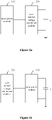
- FIG. 1a and Figure 1b are schematic diagrams of a device for suppressing potential induced degradation according to a first embodiment of the present disclosure.
- the device for suppressing potential induced degradation according to the embodiment is connected between an alternating current output terminal of a converter and a grid-connected power frequency transformer in a photovoltaic system.
- the device includes a rectification module 100, a non-isolated voltage conversion module 200 and at least one capacitor C.
- an input terminal of the rectification module 100 is connected to an output terminal of the converter, and the rectification module 100 is configured to rectify an alternating current outputted by the converter into a direct current.
- the non-isolated voltage conversion module 200 is configured to perform voltage conversion on the direct current outputted by the rectification module, and the voltage conversion is boost conversion or voltage reverse conversion.
- an input terminal of the non-isolated voltage conversion module 200 is connected to an output terminal of the converter, the non-isolated voltage conversion module 200 is configured to perform voltage conversion on an alternating current outputted by the converter, and the voltage conversion is boost conversion.
- the rectification module 100 is configured to rectify an alternating current outputted by the non-isolated voltage conversion module into a direct current.
- the capacitor C is connected in parallel with an output terminal of the direct current, and either a positive electrode or a negative electrode of the capacitor C is grounded.
- the converter may be an inverter.
- PV+ and PV- of a direct current of the converter are generally symmetrical with respect to a point N, i.e., a voltage of PV+ relative to N is the same as a voltage of N relative to PV-.
- N is an alternating current neutral point potential, and is generally formed by a midpoint of Y-type windings on the primary side of a grid-connected transformer on an alternating current side.
- the non-isolated voltage conversion module 200 implements the function of boosting or reversing a voltage, but the function can not be reducing the voltage. Since a voltage range outputted on the direct current side is smaller than a voltage range of a power grid in a case that the non-isolated voltage conversion module 200 implements the function of reducing the voltage, a highest point or a lowest point of the voltage can not be formed.
- the negative electrode of the capacitor C is grounded. It can be understood that the positive electrode of the capacitor C may be grounded. In a case that the negative electrode of the capacitor C is grounded, a voltage to earth of the photovoltaic system is completely positive. In a case that the positive electrode of the capacitor C is grounded, the voltage to earth of the photovoltaic system is completely negative.
- the device according to the embodiment can provides a highest potential point or a lowest potential point to the photovoltaic system.
- the highest potential of the photovoltaic system is zero.
- the negative electrode of the capacitor is grounded, the lowest potential of the photovoltaic system is zero.
- an output voltage of the photovoltaic system can be forced to be higher than zero or lower than zero. In such way, the unipolarity of the output voltage of the photovoltaic system can be achieved, thereby achieving a function of resisting the PID.
- non-isolated voltage conversion module can be implemented in a variety of ways. Hereinafter specific implementations will be described in detail in conjunction with drawings.
- the non-isolated voltage conversion module is any one of a Boost circuit, a Buck-boost circuit, a Cuk circuit, a Sepic circuit and a Zeta circuit, in a case that the input terminal of the rectification module 100 is connected to the output terminal of the converter.
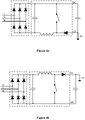
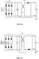
- the description is made by taking a case that the rectification module 100 is an uncontrolled rectification bridge as an example. As shown in Figure 2a , the uncontrolled rectification bridge is a three phase full-bridge circuit.
- the description is made by taking a case that the non-isolated voltage conversion module is a Buck-boost circuit 2001 as an example.
- An output terminal of the Buck-boost circuit 2001 is connected in parallel with the capacitor C.
- An output voltage of the non-isolated voltage conversion module is controlled to make a voltage to earth of the photovoltaic system negative, in a case that the positive electrode of the capacitor C is grounded.
- the output voltage of the non-isolated voltage conversion module is controlled to make the voltage to earth of the photovoltaic system positive, in a case that the negative electrode of the capacitor is grounded.
- the device according to Figure 2b may make the voltage to earth of the photovoltaic system positive.
- the photovoltaic system may include one converter, or multiple converters output terminals of which are connected in parallel.
- the description is made by taking a case that the photovoltaic system includes multiple converters and the converter is an inverter as an example.
- the Buck-boost circuit 2001 is controlled to make a negative electrode DC- of a direct voltage of the output voltage of the Buck-boost circuit 2001 lower than PV1-. Since DC- is grounded, the voltage to earth of the photovoltaic system is completely positive.
- a voltage effective value in an alternating current phase of the photovoltaic system is 230V
- DC- (DC+)-( ⁇ DC) ⁇ -500V (relative to the point N). Since DC- is grounded (PE), i.e., the voltage of the point N relative to PE is higher than 500V , the lowest voltage PV1- of the photovoltaic system relative to the ground is higher than zero.
- Figure 3b is an effect schematic diagram corresponding to Figure 2a . It can be seen from Figure 3b that, in a case that DC+ is grounded, the inverter is controlled to make a positive electrode DC+ of the direct voltage of the output voltage higher than PV1+. Since DC+ is grounded, the voltage to earth of the photovoltaic system is completely negative.
- a third embodiment of a device is described below.
- FIGS. 4a and Figure 4b are schematic diagrams of a device according to a third embodiment of the present disclosure.
- an input terminal of the rectification module 100 is connected to an output terminal of the converter and the non-isolated voltage conversion module is a Boost circuit 2002
- an output terminal of the Boost circuit 2002 is connected in parallel with the capacitor C.
- an output voltage of the non-isolated voltage conversion module is controlled to make a voltage to earth of the photovoltaic system positive, in a case that the negative electrode of the capacitor C is grounded.
- an output voltage of the non-isolated voltage conversion module is controlled to make the voltage to earth of the photovoltaic system negative, in a case that the positive electrode of the capacitor C is grounded.
- the device according to Figure 4a may make the voltage to earth of the photovoltaic system positive.
- Boost circuit is controlled to make a negative electrode DC- of a direct voltage of the output voltage of the Boost circuit lower than PV1-. Since DC- is grounded, the voltage to earth of the photovoltaic system is completely positive.
- a voltage effective value in an alternating current phase of the photovoltaic system is 230V
- DC- (DC+)-( ⁇ DC) ⁇ -500V (relative to the point N). Since DC- is grounded (PE), i.e., the voltage of the point N relative to PE is higher than 500V, the lowest voltage PV1- of the photovoltaic system relative to the ground is higher than zero.
- Figure 5b is an effect schematic diagram corresponding to Figure 4b . It can be seen from Figure 5b that, in a case that DC+ is grounded, the inverter is controlled to make a positive electrode DC+ of the direct voltage of the output voltage higher than PV1+. Since DC+ is grounded, the voltage to earth of the photovoltaic system is completely negative.
- a fourth embodiment of a device is described below.
- the non-isolated voltage conversion module is an isolated DC-DC converter based on a high-frequency transformer
- the isolated DC-DC converter includes any one of a forward converter, a fly-back converter, an LLC converter, a half-bridge isolated converter, a full-bridge isolated converter and a push-pull converter.
- An input negative electrode and an output positive electrode of the isolated DC-DC converter are connected, or an input positive electrode and an output negative electrode of the isolated DC-DC converter are connected.
- the high frequency transformer is relative to the power frequency transformer.
- the non-isolated voltage conversion module may be implemented by an isolated DC-DC converter, which may be changed into a non-isolated voltage conversion module as long as the isolation of the isolated DC-DC converter is destroyed.
- An input terminal and an output terminal of the isolated DC-DC converter may be connected to destroy the isolation of the isolated DC-DC converter.
- the input positive electrode and the output positive electrode of the isolated DC-DC converter are connected, or the input negative electrode and the output negative electrode of the isolated DC-DC converter are connected, or the input positive electrode and the output negative electrode of the isolated DC-DC converter are connected, or the input negative electrode and the output positive electrode of the isolated DC-DC converter are connected.
- the isolated DC-DC converter is the fly-back converter
- an input negative electrode and an output positive electrode of the fly-back converter are connected
- an output terminal of the fly-back converter is connected in parallel with the capacitor
- the negative electrode of the capacitor is grounded.
- the isolation of the fly-back converter 600 is destroyed, and the fly-back converter 600 equals to a non-isolated converter.
- the voltages to earth of the photovoltaic system may be completely positive by controlling the output voltage of the fly-back converter.
- the isolated DC-DC converter is the fly-back converter
- an input positive electrode and an output negative electrode of the fly-back converter are connected
- an output terminal of the fly-back converter is connected in parallel with the capacitor
- the positive electrode of the capacitor is grounded.
- the voltages to earth of the photovoltaic system may be completely negative by controlling the output voltage of the fly-back converter.
- a fifth embodiment of a device is described below.
- the non-isolated voltage conversion module is a power frequency transformer T.
- Both a primary side and a secondary side of the power frequency transformer T have Y-type structures, a neutral point of the primary side is connected with a neutral point of the secondary side, the primary side is connected to a power grid, and the secondary side is connected to the input terminal of the rectification module 100.
- the neutral point of the primary side is connected with the neutral point of the secondary side to destroy the isolation of the transformer T.
- the power frequency transformer as shown in Figure 7 is a three phase transformer including three phases which are U, V and W.
- a boosting ratio of the power frequency transformer is adjusted to make a voltage to earth of the photovoltaic system positive, in a case that the negative electrode of the capacitor C is grounded.
- the boosting ratio of the power frequency transformer is adjusted to make the voltage to earth of the photovoltaic system negative, in a case that the positive electrode of the capacitor C is grounded, which is not shown in the drawings.
- the positive electrode or the negative electrode of the capacitor C being grounded corresponds to a positive terminal DC+ or a negative terminal DC- of the output direct current being grounded respectively.
- a sixth embodiment of a device is described below.
- FIG. 8 is a schematic diagram of a device according to the sixth embodiment of the present disclosure.
- the rectification module and the non-isolated voltage conversion module are implemented by different circuits.
- the rectification module and the non-isolated voltage conversion module are not separated, but implemented by one circuit, that is, a PWM rectifier 800.
- the device according to the embodiment is connected between an alternating current output terminal of a converter and a grid-connected power frequency transformer in a photovoltaic system.
- the device includes a rectification module, a non-isolated voltage conversion module and at least one capacitor.
- the rectification module and the non-isolated voltage conversion module are implemented by the PWM rectifier 800.
- An input terminal of the PWM rectifier 800 is connected to an output terminal of the converter.
- the PWM rectifier 800 is configured to rectify an alternating current outputted by the converter into a direct current and perform voltage conversion on the alternating current, and the voltage conversion is boost conversion.
- the capacitor C is connected in parallel with an output terminal of the direct current, and either a positive electrode or a negative electrode of the capacitor C is grounded.
- Figure 8 shows a case that the negative electrode of the capacitor C is grounded.
- the output voltage of the non-isolated voltage conversion module is controlled to make the voltage to earth of the whole photovoltaic system completely positive, for details of which Figure 9 may be referred.
- the output voltage of the non-isolated voltage conversion module is controlled to make the voltage to earth of the whole photovoltaic system completely negative, in a case that the positive electrode of the capacitor C is grounded,
- a photovoltaic system is further provided according to the present disclosure, which will be described below in detail in conjunction with drawings.
- FIG 10 is a schematic diagram of a photovoltaic system according to an embodiment of the present disclosure.
- the photovoltaic system according to the embodiment includes the device for suppressing potential induced degradation according to the above embodiments, and a PV array, a converter and a transformer.
- the PV array is a photovoltaic array.
- the PV array may include multiple photovoltaic solar panels, which are connected in series, or connected in parallel, or connected in series and in parallel.
- the PV array is connected to an input terminal of the converter, an output terminal of the converter is connected to an input terminal of the transformer, and an output terminal of the transformer is connected to a power grid or a load.
- the number of converters is one or the number of converters is two or more.
- an input terminal of each of the converters is connected to one PV array, output terminals of all the converters are connected in parallel, and then the output terminals of all the converters are connected with the input terminal of the transformer.
- Figure 10 takes an example that there are multiple converters, and that the output terminals of all the converters are connected in parallel.
- a positive output terminal of the device 1000 is grounded, which may ensure voltages to earth of the whole photovoltaic system to be negative. In a case that a negative output terminal of the device 1000 is grounded, it may be ensured that the voltages to earth of the whole photovoltaic system to be positive.
- the converter is a multi-stage converter, for example, a two-stage converter including a DC-DC converter and a DC-AC converter
- PV+ and PV- of a direct current of the converter will be no longer symmetrical with respect to the N point when the front-stage DC-DC converter operates.
- the effect of suppressing PID can be achieved, as long as the device according to the present disclosure forms a lowest potential or a highest potential of the photovoltaic system at a direct output terminal, and a terminal corresponding to an output capacitor is grounded. Therefore, the present disclosure is equally applicable in a case of the multi-stage converter, or in other case that PV+ and PV- of the direct current are asymmetric with respect to the N point.
- the above-described device for suppressing potential induced degradation may further include a current limiting circuit, which may be connected in series between an output terminal on the direct current side and the ground.
- the current limiting circuit is located in the device, is connected in series with any of circuits in the device, and plays a role in limiting a current.
- the current limiting circuit includes at least one of a resistor and an inductor. It can be understood that the current limiting circuit may be only a resistor, or only an inductor, or resistors and inductors connected in series, or resistors and inductors connected in parallel, or resistors and inductors connected in series and in parallel.
- the current limiting circuit in the embodiment is to suppress a leakage current of the photovoltaic system flowing through the device, and to suppress a transient over-current when the device for suppressing potential induced degradation is newly connected to the photovoltaic system, or to prevent an current outputted by a compensation power supply from being too large in a case that impedance to earth of the photovoltaic system is too low.
- the device for suppressing potential induced degradation may further include a switch or a fuse.
- Both the switch and the fuse are for protection in a case of an accident, and are connected in series between the device and the power grid.
- the fuse may play a protective role by fusing timely in the case of over-current.
- the switch is turned off in a case that a current is large, or keeps in an off state to the photovoltaic system before the device for suppressing potential induced degradation is powered on.
- the device for suppressing potential induced degradation is close to the power grid, and a surge protection circuit is provided in consideration of the influence of the surge on the power grid side. That is, the device may further include the surge protection circuit, which may be connected in series between the device and the power grid.
Landscapes
- Engineering & Computer Science (AREA)
- Power Engineering (AREA)
- Inverter Devices (AREA)
- Supply And Distribution Of Alternating Current (AREA)
- Dc-Dc Converters (AREA)
Applications Claiming Priority (2)
| Application Number | Priority Date | Filing Date | Title |
|---|---|---|---|
| CN201610316246.9A CN105915172B (zh) | 2016-05-11 | 2016-05-11 | 一种抑制电势诱导衰减的装置及系统 |
| EP17163843.0A EP3244506B1 (fr) | 2016-05-11 | 2017-03-30 | Dispositif et système permettant de supprimer une dégradation induite de potentiel |
Related Parent Applications (2)
| Application Number | Title | Priority Date | Filing Date |
|---|---|---|---|
| EP17163843.0A Division-Into EP3244506B1 (fr) | 2016-05-11 | 2017-03-30 | Dispositif et système permettant de supprimer une dégradation induite de potentiel |
| EP17163843.0A Division EP3244506B1 (fr) | 2016-05-11 | 2017-03-30 | Dispositif et système permettant de supprimer une dégradation induite de potentiel |
Publications (1)
| Publication Number | Publication Date |
|---|---|
| EP4007113A1 true EP4007113A1 (fr) | 2022-06-01 |
Family
ID=56748930
Family Applications (2)
| Application Number | Title | Priority Date | Filing Date |
|---|---|---|---|
| EP22152040.6A Withdrawn EP4007113A1 (fr) | 2016-05-11 | 2017-03-30 | Dispositif et système permettant de supprimer une dégradation induite de potentiel |
| EP17163843.0A Active EP3244506B1 (fr) | 2016-05-11 | 2017-03-30 | Dispositif et système permettant de supprimer une dégradation induite de potentiel |
Family Applications After (1)
| Application Number | Title | Priority Date | Filing Date |
|---|---|---|---|
| EP17163843.0A Active EP3244506B1 (fr) | 2016-05-11 | 2017-03-30 | Dispositif et système permettant de supprimer une dégradation induite de potentiel |
Country Status (4)
| Country | Link |
|---|---|
| US (2) | US11101661B2 (fr) |
| EP (2) | EP4007113A1 (fr) |
| CN (1) | CN105915172B (fr) |
| ES (1) | ES2916090T3 (fr) |
Families Citing this family (22)
| Publication number | Priority date | Publication date | Assignee | Title |
|---|---|---|---|---|
| CN106505626B (zh) * | 2016-12-21 | 2019-04-09 | 阳光电源股份有限公司 | 一种光伏逆变系统及其pid效应补偿方法和装置 |
| DE102017202208A1 (de) * | 2017-02-13 | 2018-08-16 | Siemens Aktiengesellschaft | Versorgungseinrichtung für ein elektrisches Modul mit Sicherungselement |
| JP6711296B2 (ja) * | 2017-02-15 | 2020-06-17 | オムロン株式会社 | 電源システム、dc/dcコンバータ及びパワーコンディショナ |
| CN106899036B (zh) * | 2017-03-16 | 2024-03-12 | 特变电工西安电气科技有限公司 | 一种防电势诱导衰减的光伏发电系统 |
| CN107230997A (zh) * | 2017-05-11 | 2017-10-03 | 华为技术有限公司 | 一种光伏发电系统 |
| CN107492905B (zh) * | 2017-08-22 | 2020-09-29 | 上能电气股份有限公司 | 一种交流共模电压调节装置及应用该装置的光伏系统 |
| CN108306612B (zh) | 2017-12-20 | 2019-11-26 | 华为技术有限公司 | 一种光伏电站中的光伏组件衰减修复方法和装置 |
| CN110609064A (zh) * | 2018-06-14 | 2019-12-24 | 深圳碳森科技有限公司 | 一种差分阻抗电位型生物传感器及其制造方法 |
| CN108649830B (zh) * | 2018-06-28 | 2023-10-03 | 东君新能源有限公司 | 一种高频隔离逆变器以及太阳能发电系统 |
| TWI863918B (zh) * | 2018-09-26 | 2024-12-01 | 義大利商埃格特羅尼克工程股份公司 | 用於傳輸電力至具轉換器之電力負載之裝置 |
| WO2020144696A1 (fr) * | 2019-01-13 | 2020-07-16 | Vigdu V Technologies Ltd | Procédé et dispositif de décalage cc destinés à réduire la dégradation induite par le potentiel (pid) |
| KR102274958B1 (ko) * | 2019-04-15 | 2021-07-08 | 주식회사 에스제이솔루션 | 지능형 프리 레귤레이터를 이용한 전원공급장치 |
| EP4344044A3 (fr) * | 2019-08-28 | 2024-05-29 | Huawei Digital Power Technologies Co., Ltd. | Onduleur de système de production d'énergie photovoltaïque connecté au réseau, appareil de démarrage, procédé et système |
| CN110768300B (zh) * | 2019-12-11 | 2021-09-03 | 阳光电源股份有限公司 | 一种风光互补发电系统 |
| EP4102672A1 (fr) * | 2021-06-08 | 2022-12-14 | FIMER S.p.A. | Onduleur multicanal destiné à une installation photovoltaïque |
| CN113949304B (zh) * | 2021-10-19 | 2024-07-19 | 浙江德升新能源科技有限公司 | 一种pcs并联共模环流的下垂控制方法 |
| CN114400912A (zh) * | 2021-12-15 | 2022-04-26 | 固德威技术股份有限公司 | 电势诱导衰减预防电路和应用其的光伏系统 |
| CN114499157A (zh) * | 2022-02-21 | 2022-05-13 | 华为数字能源技术有限公司 | 电压变换单元、逆变器及光伏发电系统 |
| CN115276549B (zh) * | 2022-09-30 | 2022-12-27 | 锦浪科技股份有限公司 | 一种pid效应抑制系统 |
| CN116388276A (zh) * | 2023-04-13 | 2023-07-04 | 爱士惟科技股份有限公司 | 一种光伏逆变系统和pid效应抑制装置 |
| CN116207789B (zh) * | 2023-05-06 | 2023-07-21 | 锦浪科技股份有限公司 | 一种基于零序的pid效应抑制方法 |
| CN116232216A (zh) * | 2023-05-08 | 2023-06-06 | 深圳市首航新能源股份有限公司 | Pid修复电路、逆变器与光伏系统 |
Citations (8)
| Publication number | Priority date | Publication date | Assignee | Title |
|---|---|---|---|---|
| DE2428257A1 (de) * | 1974-06-12 | 1976-01-02 | Frako Kondensator Apparate | Modulare stromversorgung |
| US20070070654A1 (en) * | 2005-09-27 | 2007-03-29 | Ching-Hsiung Liu | Voltage supplying apparatus using a fuel cell |
| US20120280571A1 (en) * | 2009-12-23 | 2012-11-08 | Control Techniques Ltd | Voltage compensation |
| CN203166494U (zh) * | 2013-03-26 | 2013-08-28 | 阳光电源(上海)有限公司 | 一种解决电势诱导衰减的装置 |
| CN104300584A (zh) * | 2014-11-07 | 2015-01-21 | 深圳市永联科技有限公司 | 一种高安全性的pid效应抑制方法 |
| CN104901618A (zh) * | 2015-05-27 | 2015-09-09 | 华为技术有限公司 | 一种供电系统及供电方法 |
| CN104901378A (zh) * | 2015-04-17 | 2015-09-09 | 丁振荣 | 一种移动电源 |
| US20160116925A1 (en) * | 2014-10-28 | 2016-04-28 | Advanced Charging Technologies, LLC | Electrical circuit for delivering power to consumer electronic devices |
Family Cites Families (13)
| Publication number | Priority date | Publication date | Assignee | Title |
|---|---|---|---|---|
| GB0904572D0 (en) | 2009-03-18 | 2009-04-29 | Rolls Royce Plc | A method of forming an internal structure in a hollow component |
| JP5320144B2 (ja) * | 2009-04-16 | 2013-10-23 | 本田技研工業株式会社 | 太陽電池の最大出力電力追従制御装置 |
| US8558517B2 (en) * | 2011-09-15 | 2013-10-15 | Compuware Technology Inc. | Power supply with virtual by-pass system |
| EP2907229A4 (fr) * | 2012-10-15 | 2017-07-05 | Maxout Renewables, Inc. | Convertisseur à transfert indirect isolé |
| WO2014194081A1 (fr) * | 2013-05-29 | 2014-12-04 | Lutron Electronics Co., Inc. | Dispositif de commande de charge pour une source de lumière à diodes électroluminescentes |
| CN203697986U (zh) | 2014-01-07 | 2014-07-09 | 北汽福田汽车股份有限公司 | 电动汽车车载太阳能供电系统 |
| US9716466B2 (en) * | 2014-01-23 | 2017-07-25 | Lg Electronics Inc. | Power conversion apparatus, photovoltaic module and communication device and photovoltaic system including the same |
| SG10201401850RA (en) * | 2014-04-25 | 2015-11-27 | Rockwell Automation Asia Pacific Business Ct Pte Ltd | Motor Drive Switched Mode Power Supply Systems And Methods |
| CN103973217B (zh) * | 2014-05-19 | 2017-01-18 | 上能电气股份有限公司 | 一种抑制电池板pid效应的装置 |
| JP6374261B2 (ja) * | 2014-08-01 | 2018-08-15 | ローム株式会社 | 絶縁同期整流型dc/dcコンバータおよびその同期整流コントローラ、それを用いた電源装置、電源アダプタおよび電子機器 |
| CN104201981B (zh) * | 2014-09-25 | 2017-01-11 | 阳光电源股份有限公司 | 一种反电势诱导衰减的控制方法及控制系统 |
| CN204168221U (zh) * | 2014-10-22 | 2015-02-18 | 晶澳(扬州)太阳能光伏工程有限公司 | 一种采用非隔离逆变器的太阳能光伏组件的抗pid装置 |
| CN104393833A (zh) * | 2014-11-21 | 2015-03-04 | 南车株洲电力机车研究所有限公司 | 一种光伏智能电源 |
-
2016
- 2016-05-11 CN CN201610316246.9A patent/CN105915172B/zh active Active
-
2017
- 2017-03-30 ES ES17163843T patent/ES2916090T3/es active Active
- 2017-03-30 US US15/474,086 patent/US11101661B2/en active Active
- 2017-03-30 EP EP22152040.6A patent/EP4007113A1/fr not_active Withdrawn
- 2017-03-30 EP EP17163843.0A patent/EP3244506B1/fr active Active
-
2021
- 2021-07-13 US US17/374,297 patent/US11973349B2/en active Active
Patent Citations (10)
| Publication number | Priority date | Publication date | Assignee | Title |
|---|---|---|---|---|
| DE2428257A1 (de) * | 1974-06-12 | 1976-01-02 | Frako Kondensator Apparate | Modulare stromversorgung |
| US20070070654A1 (en) * | 2005-09-27 | 2007-03-29 | Ching-Hsiung Liu | Voltage supplying apparatus using a fuel cell |
| US20120280571A1 (en) * | 2009-12-23 | 2012-11-08 | Control Techniques Ltd | Voltage compensation |
| CN203166494U (zh) * | 2013-03-26 | 2013-08-28 | 阳光电源(上海)有限公司 | 一种解决电势诱导衰减的装置 |
| US20160116925A1 (en) * | 2014-10-28 | 2016-04-28 | Advanced Charging Technologies, LLC | Electrical circuit for delivering power to consumer electronic devices |
| CN104300584A (zh) * | 2014-11-07 | 2015-01-21 | 深圳市永联科技有限公司 | 一种高安全性的pid效应抑制方法 |
| CN104901378A (zh) * | 2015-04-17 | 2015-09-09 | 丁振荣 | 一种移动电源 |
| CN104901618A (zh) * | 2015-05-27 | 2015-09-09 | 华为技术有限公司 | 一种供电系统及供电方法 |
| WO2016188433A1 (fr) * | 2015-05-27 | 2016-12-01 | 华为技术有限公司 | Système et procédé d'alimentation électrique |
| EP3291441A1 (fr) * | 2015-05-27 | 2018-03-07 | Huawei Technologies Co., Ltd. | Système et procédé d'alimentation électrique |
Non-Patent Citations (1)
| Title |
|---|
| CHONGMING QIAO ET AL: "A General Three-Phase PFC Controller for Rectifiers With a Parallel-Connected Dual Boost Topology", IEEE TRANSACTIONS ON POWER ELECTRONICS, INSTITUTE OF ELECTRICAL AND ELECTRONICS ENGINEERS, USA, vol. 17, no. 6, 1 November 2002 (2002-11-01), XP011078241, ISSN: 0885-8993 * |
Also Published As
| Publication number | Publication date |
|---|---|
| US20170331294A1 (en) | 2017-11-16 |
| EP3244506B1 (fr) | 2022-03-30 |
| US20210344202A1 (en) | 2021-11-04 |
| EP3244506A1 (fr) | 2017-11-15 |
| CN105915172A (zh) | 2016-08-31 |
| US11101661B2 (en) | 2021-08-24 |
| US11973349B2 (en) | 2024-04-30 |
| CN105915172B (zh) | 2017-12-22 |
| ES2916090T3 (es) | 2022-06-28 |
Similar Documents
| Publication | Publication Date | Title |
|---|---|---|
| US11973349B2 (en) | Device for suppressing potential induced degradation and system | |
| US11005268B2 (en) | Optimizer, control method and parallel arrangement for photovoltaic system | |
| EP3163734B1 (fr) | Convertisseur continu-continu à rapport de transformation élevé | |
| US7193872B2 (en) | Solar array inverter with maximum power tracking | |
| US8098055B2 (en) | Step-up converter systems and methods | |
| US9525364B2 (en) | Smart grid power converter | |
| CN107210684B (zh) | 五电平拓扑单元及五电平逆变器 | |
| US20080037305A1 (en) | Monopolar dc to bipolar dc to ac converter | |
| CN107959433B (zh) | 一种抑制漏电流的逆变器及逆变系统 | |
| EP3038246B1 (fr) | Topologie de circuit à conversion continu-alternatif | |
| US20200295570A1 (en) | System and Device for Exporting Power, and Method of Configuring Thereof | |
| CN105680793B (zh) | 一种光伏系统的电压补偿装置及光伏系统 | |
| US10199935B2 (en) | Hybrid boosting converters | |
| TWI685169B (zh) | 雙向儲能系統 | |
| KR101034263B1 (ko) | 태양광 발전용 dc-dc 컨버터 | |
| US20160142007A1 (en) | Photovoltaic inverter | |
| CN111371323A (zh) | 一种boost升压功率变换电路及其控制方法 | |
| US10965220B2 (en) | Non-isolated inverting apparatus, control method thereof and photovoltaic system having the same | |
| EP3776830B1 (fr) | Convertisseur de courant comprenant un dispositif d'amortissement de recirculation | |
| de Oliveira et al. | Operation of a high gain bidirectional DC-DC converter for photovoltaic on-grid systems | |
| Kim et al. | Commutation technique for high frequency link inverter without operational limitations and dead time | |
| Ho et al. | Switched-capacitor embedded quasi-Z-source inverters with advanced boosting capability | |
| CN222029833U (zh) | 逆变器和光伏发电系统 | |
| Al Mamun et al. | A Novel High Gain DC-DC Step up Converter | |
| Manoharan et al. | Low cost single-sourced asymmetrical cascaded H-bridge multilevel inverter |
Legal Events
| Date | Code | Title | Description |
|---|---|---|---|
| PUAI | Public reference made under article 153(3) epc to a published international application that has entered the european phase |
Free format text: ORIGINAL CODE: 0009012 |
|
| STAA | Information on the status of an ep patent application or granted ep patent |
Free format text: STATUS: REQUEST FOR EXAMINATION WAS MADE |
|
| STAA | Information on the status of an ep patent application or granted ep patent |
Free format text: STATUS: EXAMINATION IS IN PROGRESS |
|
| 17P | Request for examination filed |
Effective date: 20220118 |
|
| AC | Divisional application: reference to earlier application |
Ref document number: 3244506 Country of ref document: EP Kind code of ref document: P |
|
| AK | Designated contracting states |
Kind code of ref document: A1 Designated state(s): AL AT BE BG CH CY CZ DE DK EE ES FI FR GB GR HR HU IE IS IT LI LT LU LV MC MK MT NL NO PL PT RO RS SE SI SK SM TR |
|
| 17Q | First examination report despatched |
Effective date: 20220520 |
|
| STAA | Information on the status of an ep patent application or granted ep patent |
Free format text: STATUS: THE APPLICATION HAS BEEN WITHDRAWN |
|
| 18W | Application withdrawn |
Effective date: 20240607 |