EP4009025A1 - Agent de liaison comprenant un noyau et un revêtement - Google Patents
Agent de liaison comprenant un noyau et un revêtement Download PDFInfo
- Publication number
- EP4009025A1 EP4009025A1 EP20212258.6A EP20212258A EP4009025A1 EP 4009025 A1 EP4009025 A1 EP 4009025A1 EP 20212258 A EP20212258 A EP 20212258A EP 4009025 A1 EP4009025 A1 EP 4009025A1
- Authority
- EP
- European Patent Office
- Prior art keywords
- core
- metallic material
- bonding
- connection means
- jacket
- Prior art date
- Legal status (The legal status is an assumption and is not a legal conclusion. Google has not performed a legal analysis and makes no representation as to the accuracy of the status listed.)
- Withdrawn
Links
Images


Classifications
-
- G—PHYSICS
- G01—MEASURING; TESTING
- G01K—MEASURING TEMPERATURE; MEASURING QUANTITY OF HEAT; THERMALLY-SENSITIVE ELEMENTS NOT OTHERWISE PROVIDED FOR
- G01K7/00—Measuring temperature based on the use of electric or magnetic elements directly sensitive to heat ; Power supply therefor, e.g. using thermoelectric elements
- G01K7/16—Measuring temperature based on the use of electric or magnetic elements directly sensitive to heat ; Power supply therefor, e.g. using thermoelectric elements using resistive elements
- G01K7/18—Measuring temperature based on the use of electric or magnetic elements directly sensitive to heat ; Power supply therefor, e.g. using thermoelectric elements using resistive elements the element being a linear resistance, e.g. platinum resistance thermometer
- G01K7/183—Measuring temperature based on the use of electric or magnetic elements directly sensitive to heat ; Power supply therefor, e.g. using thermoelectric elements using resistive elements the element being a linear resistance, e.g. platinum resistance thermometer characterised by the use of the resistive element
-
- G—PHYSICS
- G01—MEASURING; TESTING
- G01K—MEASURING TEMPERATURE; MEASURING QUANTITY OF HEAT; THERMALLY-SENSITIVE ELEMENTS NOT OTHERWISE PROVIDED FOR
- G01K7/00—Measuring temperature based on the use of electric or magnetic elements directly sensitive to heat ; Power supply therefor, e.g. using thermoelectric elements
- G01K7/16—Measuring temperature based on the use of electric or magnetic elements directly sensitive to heat ; Power supply therefor, e.g. using thermoelectric elements using resistive elements
- G01K7/18—Measuring temperature based on the use of electric or magnetic elements directly sensitive to heat ; Power supply therefor, e.g. using thermoelectric elements using resistive elements the element being a linear resistance, e.g. platinum resistance thermometer
- G01K7/20—Measuring temperature based on the use of electric or magnetic elements directly sensitive to heat ; Power supply therefor, e.g. using thermoelectric elements using resistive elements the element being a linear resistance, e.g. platinum resistance thermometer in a specially-adapted circuit, e.g. bridge circuit
-
- G—PHYSICS
- G01—MEASURING; TESTING
- G01R—MEASURING ELECTRIC VARIABLES; MEASURING MAGNETIC VARIABLES
- G01R1/00—Details of instruments or arrangements of the types included in groups G01R5/00 - G01R13/00 and G01R31/00
- G01R1/20—Modifications of basic electric elements for use in electric measuring instruments; Structural combinations of such elements with such instruments
- G01R1/203—Resistors used for electric measuring, e.g. decade resistors standards, resistors for comparators, series resistors, shunts
-
- H—ELECTRICITY
- H01—ELECTRIC ELEMENTS
- H01B—CABLES; CONDUCTORS; INSULATORS; SELECTION OF MATERIALS FOR THEIR CONDUCTIVE, INSULATING OR DIELECTRIC PROPERTIES
- H01B1/00—Conductors or conductive bodies characterised by the conductive materials; Selection of materials as conductors
- H01B1/02—Conductors or conductive bodies characterised by the conductive materials; Selection of materials as conductors mainly consisting of metals or alloys
- H01B1/023—Alloys based on aluminium
-
- H—ELECTRICITY
- H01—ELECTRIC ELEMENTS
- H01B—CABLES; CONDUCTORS; INSULATORS; SELECTION OF MATERIALS FOR THEIR CONDUCTIVE, INSULATING OR DIELECTRIC PROPERTIES
- H01B1/00—Conductors or conductive bodies characterised by the conductive materials; Selection of materials as conductors
- H01B1/02—Conductors or conductive bodies characterised by the conductive materials; Selection of materials as conductors mainly consisting of metals or alloys
- H01B1/026—Alloys based on copper
-
- H—ELECTRICITY
- H10—SEMICONDUCTOR DEVICES; ELECTRIC SOLID-STATE DEVICES NOT OTHERWISE PROVIDED FOR
- H10W—GENERIC PACKAGES, INTERCONNECTIONS, CONNECTORS OR OTHER CONSTRUCTIONAL DETAILS OF DEVICES COVERED BY CLASS H10
- H10W42/00—Arrangements for protection of devices
- H10W42/80—Arrangements for protection of devices protecting against overcurrent or overload, e.g. fuses or shunts
-
- H—ELECTRICITY
- H10—SEMICONDUCTOR DEVICES; ELECTRIC SOLID-STATE DEVICES NOT OTHERWISE PROVIDED FOR
- H10W—GENERIC PACKAGES, INTERCONNECTIONS, CONNECTORS OR OTHER CONSTRUCTIONAL DETAILS OF DEVICES COVERED BY CLASS H10
- H10W44/00—Electrical arrangements for controlling or matching impedance
- H10W44/401—Resistive arrangements
-
- H—ELECTRICITY
- H10—SEMICONDUCTOR DEVICES; ELECTRIC SOLID-STATE DEVICES NOT OTHERWISE PROVIDED FOR
- H10W—GENERIC PACKAGES, INTERCONNECTIONS, CONNECTORS OR OTHER CONSTRUCTIONAL DETAILS OF DEVICES COVERED BY CLASS H10
- H10W90/00—Package configurations
-
- H—ELECTRICITY
- H10—SEMICONDUCTOR DEVICES; ELECTRIC SOLID-STATE DEVICES NOT OTHERWISE PROVIDED FOR
- H10W—GENERIC PACKAGES, INTERCONNECTIONS, CONNECTORS OR OTHER CONSTRUCTIONAL DETAILS OF DEVICES COVERED BY CLASS H10
- H10W40/00—Arrangements for thermal protection or thermal control
-
- H—ELECTRICITY
- H10—SEMICONDUCTOR DEVICES; ELECTRIC SOLID-STATE DEVICES NOT OTHERWISE PROVIDED FOR
- H10W—GENERIC PACKAGES, INTERCONNECTIONS, CONNECTORS OR OTHER CONSTRUCTIONAL DETAILS OF DEVICES COVERED BY CLASS H10
- H10W72/00—Interconnections or connectors in packages
- H10W72/071—Connecting or disconnecting
- H10W72/075—Connecting or disconnecting of bond wires
- H10W72/07531—Techniques
- H10W72/07532—Compression bonding, e.g. thermocompression bonding
- H10W72/07533—Ultrasonic bonding, e.g. thermosonic bonding
-
- H—ELECTRICITY
- H10—SEMICONDUCTOR DEVICES; ELECTRIC SOLID-STATE DEVICES NOT OTHERWISE PROVIDED FOR
- H10W—GENERIC PACKAGES, INTERCONNECTIONS, CONNECTORS OR OTHER CONSTRUCTIONAL DETAILS OF DEVICES COVERED BY CLASS H10
- H10W72/00—Interconnections or connectors in packages
- H10W72/071—Connecting or disconnecting
- H10W72/075—Connecting or disconnecting of bond wires
- H10W72/07551—Connecting or disconnecting of bond wires characterised by changes in properties of the bond wires during the connecting
- H10W72/07554—Connecting or disconnecting of bond wires characterised by changes in properties of the bond wires during the connecting changes in dispositions
-
- H—ELECTRICITY
- H10—SEMICONDUCTOR DEVICES; ELECTRIC SOLID-STATE DEVICES NOT OTHERWISE PROVIDED FOR
- H10W—GENERIC PACKAGES, INTERCONNECTIONS, CONNECTORS OR OTHER CONSTRUCTIONAL DETAILS OF DEVICES COVERED BY CLASS H10
- H10W72/00—Interconnections or connectors in packages
- H10W72/50—Bond wires
- H10W72/521—Structures or relative sizes of bond wires
- H10W72/522—Multilayered bond wires, e.g. having a coating concentric around a core
-
- H—ELECTRICITY
- H10—SEMICONDUCTOR DEVICES; ELECTRIC SOLID-STATE DEVICES NOT OTHERWISE PROVIDED FOR
- H10W—GENERIC PACKAGES, INTERCONNECTIONS, CONNECTORS OR OTHER CONSTRUCTIONAL DETAILS OF DEVICES COVERED BY CLASS H10
- H10W72/00—Interconnections or connectors in packages
- H10W72/50—Bond wires
- H10W72/531—Shapes of wire connectors
- H10W72/533—Cross-sectional shape
- H10W72/534—Cross-sectional shape being rectangular
-
- H—ELECTRICITY
- H10—SEMICONDUCTOR DEVICES; ELECTRIC SOLID-STATE DEVICES NOT OTHERWISE PROVIDED FOR
- H10W—GENERIC PACKAGES, INTERCONNECTIONS, CONNECTORS OR OTHER CONSTRUCTIONAL DETAILS OF DEVICES COVERED BY CLASS H10
- H10W72/00—Interconnections or connectors in packages
- H10W72/50—Bond wires
- H10W72/541—Dispositions of bond wires
- H10W72/543—Dispositions of bond wires of outermost layers of multilayered bond wires, e.g. coating being only on a part of a core
-
- H—ELECTRICITY
- H10—SEMICONDUCTOR DEVICES; ELECTRIC SOLID-STATE DEVICES NOT OTHERWISE PROVIDED FOR
- H10W—GENERIC PACKAGES, INTERCONNECTIONS, CONNECTORS OR OTHER CONSTRUCTIONAL DETAILS OF DEVICES COVERED BY CLASS H10
- H10W72/00—Interconnections or connectors in packages
- H10W72/50—Bond wires
- H10W72/541—Dispositions of bond wires
- H10W72/5438—Dispositions of bond wires the bond wires having multiple connections on the same bond pad
-
- H—ELECTRICITY
- H10—SEMICONDUCTOR DEVICES; ELECTRIC SOLID-STATE DEVICES NOT OTHERWISE PROVIDED FOR
- H10W—GENERIC PACKAGES, INTERCONNECTIONS, CONNECTORS OR OTHER CONSTRUCTIONAL DETAILS OF DEVICES COVERED BY CLASS H10
- H10W72/00—Interconnections or connectors in packages
- H10W72/50—Bond wires
- H10W72/541—Dispositions of bond wires
- H10W72/547—Dispositions of multiple bond wires
- H10W72/5473—Dispositions of multiple bond wires multiple bond wires connected to a common bond pad
-
- H—ELECTRICITY
- H10—SEMICONDUCTOR DEVICES; ELECTRIC SOLID-STATE DEVICES NOT OTHERWISE PROVIDED FOR
- H10W—GENERIC PACKAGES, INTERCONNECTIONS, CONNECTORS OR OTHER CONSTRUCTIONAL DETAILS OF DEVICES COVERED BY CLASS H10
- H10W72/00—Interconnections or connectors in packages
- H10W72/50—Bond wires
- H10W72/541—Dispositions of bond wires
- H10W72/547—Dispositions of multiple bond wires
- H10W72/5475—Dispositions of multiple bond wires multiple bond wires connected to common bond pads at both ends of the wires
-
- H—ELECTRICITY
- H10—SEMICONDUCTOR DEVICES; ELECTRIC SOLID-STATE DEVICES NOT OTHERWISE PROVIDED FOR
- H10W—GENERIC PACKAGES, INTERCONNECTIONS, CONNECTORS OR OTHER CONSTRUCTIONAL DETAILS OF DEVICES COVERED BY CLASS H10
- H10W72/00—Interconnections or connectors in packages
- H10W72/50—Bond wires
- H10W72/551—Materials of bond wires
- H10W72/552—Materials of bond wires comprising metals or metalloids, e.g. silver
-
- H—ELECTRICITY
- H10—SEMICONDUCTOR DEVICES; ELECTRIC SOLID-STATE DEVICES NOT OTHERWISE PROVIDED FOR
- H10W—GENERIC PACKAGES, INTERCONNECTIONS, CONNECTORS OR OTHER CONSTRUCTIONAL DETAILS OF DEVICES COVERED BY CLASS H10
- H10W72/00—Interconnections or connectors in packages
- H10W72/50—Bond wires
- H10W72/551—Materials of bond wires
- H10W72/552—Materials of bond wires comprising metals or metalloids, e.g. silver
- H10W72/5522—Materials of bond wires comprising metals or metalloids, e.g. silver comprising gold [Au]
-
- H—ELECTRICITY
- H10—SEMICONDUCTOR DEVICES; ELECTRIC SOLID-STATE DEVICES NOT OTHERWISE PROVIDED FOR
- H10W—GENERIC PACKAGES, INTERCONNECTIONS, CONNECTORS OR OTHER CONSTRUCTIONAL DETAILS OF DEVICES COVERED BY CLASS H10
- H10W72/00—Interconnections or connectors in packages
- H10W72/50—Bond wires
- H10W72/551—Materials of bond wires
- H10W72/552—Materials of bond wires comprising metals or metalloids, e.g. silver
- H10W72/5524—Materials of bond wires comprising metals or metalloids, e.g. silver comprising aluminium [Al]
-
- H—ELECTRICITY
- H10—SEMICONDUCTOR DEVICES; ELECTRIC SOLID-STATE DEVICES NOT OTHERWISE PROVIDED FOR
- H10W—GENERIC PACKAGES, INTERCONNECTIONS, CONNECTORS OR OTHER CONSTRUCTIONAL DETAILS OF DEVICES COVERED BY CLASS H10
- H10W72/00—Interconnections or connectors in packages
- H10W72/50—Bond wires
- H10W72/551—Materials of bond wires
- H10W72/552—Materials of bond wires comprising metals or metalloids, e.g. silver
- H10W72/5525—Materials of bond wires comprising metals or metalloids, e.g. silver comprising copper [Cu]
-
- H—ELECTRICITY
- H10—SEMICONDUCTOR DEVICES; ELECTRIC SOLID-STATE DEVICES NOT OTHERWISE PROVIDED FOR
- H10W—GENERIC PACKAGES, INTERCONNECTIONS, CONNECTORS OR OTHER CONSTRUCTIONAL DETAILS OF DEVICES COVERED BY CLASS H10
- H10W72/00—Interconnections or connectors in packages
- H10W72/50—Bond wires
- H10W72/551—Materials of bond wires
- H10W72/555—Materials of bond wires of outermost layers of multilayered bond wires, e.g. material of a coating
-
- H—ELECTRICITY
- H10—SEMICONDUCTOR DEVICES; ELECTRIC SOLID-STATE DEVICES NOT OTHERWISE PROVIDED FOR
- H10W—GENERIC PACKAGES, INTERCONNECTIONS, CONNECTORS OR OTHER CONSTRUCTIONAL DETAILS OF DEVICES COVERED BY CLASS H10
- H10W72/00—Interconnections or connectors in packages
- H10W72/90—Bond pads, in general
- H10W72/921—Structures or relative sizes of bond pads
- H10W72/926—Multiple bond pads having different sizes
-
- H—ELECTRICITY
- H10—SEMICONDUCTOR DEVICES; ELECTRIC SOLID-STATE DEVICES NOT OTHERWISE PROVIDED FOR
- H10W—GENERIC PACKAGES, INTERCONNECTIONS, CONNECTORS OR OTHER CONSTRUCTIONAL DETAILS OF DEVICES COVERED BY CLASS H10
- H10W90/00—Package configurations
- H10W90/701—Package configurations characterised by the relative positions of pads or connectors relative to package parts
- H10W90/751—Package configurations characterised by the relative positions of pads or connectors relative to package parts of bond wires
- H10W90/754—Package configurations characterised by the relative positions of pads or connectors relative to package parts of bond wires between a chip and a stacked insulating package substrate, interposer or RDL
Definitions
- the invention relates to a bonding agent for connecting a semiconductor element to a substrate.
- the invention relates to a semiconductor module with at least one semiconductor element, a substrate and at least one such bond connection means.
- the invention relates to a power converter with at least one semiconductor module.
- the invention relates to the use of at least one bonding agent as a gate resistor, as a shunt, as a resistor in an RC filter, or as a safety fuse in a semiconductor module.
- the invention relates to the use of at least one bond connection means for current measurement or temperature determination in a semiconductor module.
- bonding means which are embodied, for example, as bonding wires or bonding strips, are generally used only to connect a semiconductor element to a substrate in a semiconductor module.
- a power converter is to be understood, for example, as a rectifier, an inverter, a converter or a DC voltage converter. Therefore, with such bonding means, the focus is usually on reducing parasitic resistances and parasitic inductances.
- the patent specification DE 10 2010 031 993 B4 describes a method for producing a bonding wire having a wire core made of a first material and a wire sheath encasing the wire core made of a second material, wherein the first material comprises a first metal and the second material comprises a second metal and the first metal and the second metal are different.
- EP 2 662 891 B1 describes a method of making an aluminum-coated copper bonding wire.
- shunt resistors are implemented, for example, as external resistors, which require additional installation space.
- shunt resistors are designed as internal components which are integrated in the semiconductor element, such internal components having in particular a low current carrying capacity, a high temperature drift and high costs for the space on the chip.
- a bonding connection means for connecting a semiconductor element to a substrate, having a core and a cladding that encloses the core, in particular completely, the core being made of a first metallic material and the cladding being made of a second metallic material that is different from the first metallic material Material is made and wherein the first metallic material of the core has a lower electrical conductivity than the second metallic material of the shell.
- the object is achieved according to the invention by a semiconductor module with at least one semiconductor element, a Substrate and at least one such bonding agent, wherein the semiconductor element and / or the substrate are connected to the at least one bonding agent.
- the object is achieved according to the invention by a power converter with at least one semiconductor module.
- the object is achieved according to the invention by using at least one bonding agent as a gate resistor, as a shunt, as a resistor in an RC filter, or as a safety fuse in a semiconductor module, the at least one bonding agent having a core and a jacket that encloses the core, in particular completely has, wherein the core is made of a first metallic material and the shell is made of a second metallic material different from the first metallic material and wherein the first metallic material of the core has a lower electrical conductivity than the second metallic material of the shell.
- the object is achieved according to the invention by the use of at least one bonding agent for current measurement or temperature determination in a semiconductor module, wherein the at least one bonding agent has a core and a jacket that encloses the core, in particular completely, wherein the core is made of a first metallic material and the Shell is made of a second metallic material different from the first metallic material and wherein the first metallic material of the core has a lower electrical conductivity than the second metallic material of the shell.
- the invention is based on the idea of optimizing a layout of a semiconductor module by using an existing bond connection means as a resistor and replacing an external resistor, for example, which saves installation space.
- a bonding connection means is designed, for example, as a bonding wire or bonding tape and has a core and a jacket that encloses the core, in particular completely, the core being made of a first metallic material and the jacket being made of a second metallic material that is different from the first metallic material.
- the second metallic material of the jacket which is also called jacket material or base material, is particularly suitable for being connected to a surface, eg of the substrate and/or the semiconductor element, by ultrasonic welding, for example by ultrasonic friction welding.
- the cladding material contains aluminum, copper or gold.
- the first metallic material of the core has a lower electrical conductivity than the second metallic material of the cladding.
- the first metallic material of the core contains a resistance alloy, as a result of which a high resistance can be produced with a short bonding wire length, which reduces parasitic inductance, for example.
- the replacement of a discrete shunt resistor by bonding means connected in parallel enables individual current measurements for parallel semiconductor elements due to the space saving.
- An additional saving in space is achieved, for example, by the bonding connection means designed as a shunt resistor spanning other conductors, in particular conductors applied in a structured manner on the substrate. This also allows for even greater freedom the optimization of the layout.
- the use of such a bonding agent enables a current measurement or a temperature determination.
- a current measurement is carried out, for example, by measuring a voltage drop across a bond connection means through which a current flows, with the current through the bond connection means being able to be determined on the basis of the known resistance of the bond connection means.
- the temperature is determined, for example, by measuring the voltage drop across a bond connection means through which a defined current flows and using a material-specific conversion factor to determine a temperature.
- a further embodiment provides that the electrical conductivity of the first metallic material is at most 10%, in particular at most 5%, of the electrical conductivity of the second metallic material. This is advantageous since a resistance of the bond connection means can be varied in a defined manner over a wide range.
- a further embodiment provides that the first metallic material of the core has a conductivity in the range from 0.5 MS/m to 20 MS/m, in particular in the range from 0.5 MS/m to 4 MS/m. Comparatively high defined resistances with short bonding wires can be realized with such conductivities.
- a further embodiment provides that the resistance of the first metallic material of the core has a temperature coefficient of ⁇ 0.1 ⁇ 10 -3 K -1 in the range from -40°C to 200°C. Such a flat temperature coefficient enables the realization of a defined resistance over a large temperature range.
- a further embodiment provides that the core contains zeranine, manganine, constantan or isaohm. Resistor alloys of this type make it possible thanks to their flat temperature coefficient the realization of a defined resistance over a large temperature range.
- the core contains a PTC thermistor.
- the core is made of platinum. Bonding means with such a core are suitable for temperature measurement.
- a further embodiment provides that the first metallic material of the core has a resistance with a substantially linear temperature profile.
- a linear temperature profile of the resistance is present in particular when a temperature coefficient of the second and/or third order is at least 100x, in particular 500x, smaller than a temperature coefficient of the first order.
- the core is made of Resistherm (NiFe30).
- a core designed in this way can be used to produce a bond connection means whose resistance can be set and defined by the length and/or cross-sectional geometry, with the resistance being dependent on the temperature of the bond connection means.
- a further embodiment provides that a surface portion of the core is at least 90% of the cross-sectional area of the bond connection means. This is advantageous since a resistance of the bond connection means can be varied in a defined manner over a wide range.
- the described components of the embodiments each represent individual features of the invention to be considered independently of one another, which also develop the invention independently of one another and are therefore also to be regarded as part of the invention individually or in a combination other than the one shown. Furthermore, the described embodiments can also be supplemented by further features of the invention that have already been described.
- FIG 1 shows a schematic representation of a first embodiment of a bonding connection means 2, which is designed, for example, as a bonding wire with a circular cross section. While a cross section of the bonding wire is shown on the left, a longitudinal section of the bonding wire is shown on the right.
- the bonding wire has a core 4 and a jacket 6 completely encasing the core 4, the core 4 being made from a first metal material and the jacket 6 being made from a second metal material different from the first metal material.
- a surface portion of the core 4 is at least 90% of the cross-sectional area of the bonding wire, with a diameter d of the bonding wire being in the range from 125 ⁇ m to 500 ⁇ m.
- a thickness s of the cladding is a maximum of 15 ⁇ m.
- the second metallic material which is also called cladding material or base material, is configured to produce an electrically conductive connection of a semiconductor element to a surface, in particular a substrate.
- a bonding connection of this type is produced, for example, by ultrasonic welding, in particular by ultrasonic friction welding, with the jacket material containing aluminum, copper or gold, for example.
- the first metallic material of the core 4 has a lower electrical conductivity than the cladding material, the electrical conductivity of the first metallic material being at most 10%, in particular at most 5%, of the electrical conductivity of the cladding material.
- the first metallic material of the core 4 has a defined resistance, the conductivity of the first metallic material being in the range from 0.5 MS/m to 20 MS/m, in particular in the range from 0.5 MS/m to 4 MS/m. m, lies.
- the bond wire in FIG 1 can be produced, for example, by means of wire drawing.
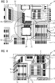
- FIG 2 1 shows a schematic representation of a semiconductor module 8 with parallel semiconductor elements 10 and bond connecting means 2 designed as gate resistors, which connect the parallel semiconductor elements 10 to a substrate 12.
- the bonding connection means 2 embodied as gate resistors are connected to a structured metallization 14 of the substrate 12 .
- the semiconductor elements 10 are each implemented as a transistor, in particular as an insulated gate bipolar transistor (IGBT), as a metal oxide semiconductor field effect transistor (MOSFET) or as a field effect transistor.
- a common supply line 15 is connected to a gate contact 16 of the respective semiconductor element 10 via a bonding connection means 2 in each case.
- Further bonding wires 18 are provided for further contacting, in particular of emitter contacts 19, of the semiconductor elements 10 with the substrate 12.
- the core 4 of the bonding agent 2 is made from a resistance alloy.
- the resistance of the first metallic material of the core 4 has a temperature coefficient of ⁇ 0.1 ⁇ 10 -3 K -1 in the range from -40°C to 200°C.
- the resistance alloy contains, for example, Zeranin, Manganin, Konstantan or Isaohm.
- the gate resistances formed by the bond connection means 2 can be individually adapted, for example by the length and/or cross-sectional geometry of the bond connection means 2, in particular for parallel semiconductor elements 10.
- the core 4 of the bond connection means 2 is made from a material with a high, in particular defined, temperature coefficient. Such a high temperature coefficient is in the range of 3*10 -3 K -1 to 10*10 -3 K -1 at 20 C.
- the first metallic material of the core 4 has a resistance with a substantially linear temperature curve.
- the core 4 contains a PTC thermistor such as platinum or Resistherm (NiFe30).
- a core 4 designed in this way can be used to produce a bond connection means 2, the resistance of which can be set and defined by the length and/or cross-sectional geometry, the resistance depending on the temperature of the bond connection means 2 is dependent.
- bond connection means 2 designed as a gate resistor also heats up when the semiconductor element 10 heats up and the resistance of the bond connection means 2 increases with increasing temperature, the semiconductor element 10 switches more slowly due to the negative current feedback and the load current is reduced.
- a balancing of the load currents can therefore be achieved by using bonding connection means 2, which have a core 4 made of a material with a high temperature coefficient, as gate resistors.
- the further execution of the bonding means 2 in FIG 2 corresponds to the in FIG 1 .
- FIG. 3 shows a schematic representation of a semiconductor module 8 with an RC filter 20, wherein a resistor 22 of the RC filter 20 is realized by, in particular five parallel, bonding means 2, while a capacitance 24 of the RC filter 20 is designed as a snubber capacitor.
- the further design of the semiconductor module 8 and the bond connection means 2 in 3 corresponds to the in FIG 2 .
- FIG 4 1 shows a schematic representation of a semiconductor module 8 with bonding connection means 2 designed as a shunt resistor 26.
- a shunt resistor 26 saves installation space, so that individual current measurements for parallel semiconductor elements 10 are made possible in a space-saving manner.
- the core 4 of the bond connection means 2 as in FIG 2 described, made of a material with a high, in particular defined, temperature coefficient.
- the core 4 contains a PTC thermistor such as platinum or Resistherm (NiFe30).
- the load current-dependent heating of the bond connection means 2 results in negative feedback: the greater the load current flowing through the bond connection means 2 of the shunt resistor 26, the higher its temperature. Since the resistance of the bond connection means 2 increases with temperature, the load current is limited.
- a symmetrical load current distribution can be optimized if the shunt resistor 26 formed in this way is connected in series with the respective semiconductor elements 10 is switched.
- the feedback is amplified by a thermal coupling of the shunt resistor 26 to the respective semiconductor element 10, for example by direct bonding of the semiconductor element 10 to the bonding connection means 2 of the shunt resistor 26.
- the further design of the semiconductor module 8 and the bond connection means 2 in FIG 4 corresponds to the in FIG 2 .
- FIG. 1 shows a schematic representation of parallel semiconductor elements 10 with bonding connection means 2 in the load current path, the parallel semiconductors being arranged on parallel semiconductor modules 8.
- FIG. The core 4 of the bonding means 2 is, as in FIG 2 described, made of a material with a high, in particular defined, temperature coefficient.
- the core 4 contains a PTC thermistor such as platinum or Resistherm (NiFe30).
- PTC thermistor such as platinum or Resistherm (NiFe30).
- a temperature-dependent resistance is thus formed in each case in the load current paths of the parallel semiconductor modules 8 by the bonding means 2, which leads to balancing across the semiconductor modules 8.
- a temperature can be determined by means of measuring devices 28 .
- the temperature is determined in particular by measuring the voltage drop at the bonding connection means 2 with a known load current and determining the temperature from this using a material-specific conversion factor.
- the bonding connection means 2 are optionally designed as a safety fuse, which heats up considerably in the event of a high overcurrent and has a very high resistance or burns out.
- the further design of the semiconductor modules 8 and the bond connection means 2 in 5 corresponds to the in FIG 2 .
- FIG. 6 shows a schematic representation of parallel semiconductor elements 10 with bond connection means 2 in the gate path. Analogous to 5 a temperature-dependent resistance is formed in the gate paths of the parallel semiconductor modules 8 by the bond connection means 2, which leads to balancing across the semiconductor modules 8. A temperature is at a known gate current by means of measuring devices 28, as in 5 described, ascertainable. The further design of the semiconductor modules 8 and the bond connection means 2 in 6 corresponds to the in 5 .
- FIG 7 shows a schematic representation of a second embodiment of a bond connection means 2, which is embodied by way of example as a bond band with a rectangular cross section. While a cross section of the bonding tape is shown on the left, a longitudinal section of the bonding tape is shown on the right.
- the bond band has a core 4 and a jacket 6 completely encasing the core 4, the core 4 being made from a first metal material and the jacket 6 being made from a second metal material which is different from the first metal material.
- the jacket 6 of the bonding tape does not enclose the core 4 completely.
- the jacket 6 of the bonding tape is connected to the core 4 in a sandwich-like manner on opposite longer sides of the rectangular cross section.
- a surface area of the core 4 is at least 90% of the cross-sectional area of the bond band, the bond band having a width b of 4 mm and a height h of 1 mm, for example.
- the invention relates to a bond connection means 2 for connecting a semiconductor element 10 to a substrate 12.
- the bond connection means 2 have a core 4 and a core 4, in particular completely, enveloping cladding 6, wherein the core 4 is made of a first metallic material and the jacket 6 is made of a second metallic material that is different from the first metallic material, and the first metallic material of the core 4 has a lower electrical conductivity than the second metallic material of the jacket 6.
Landscapes
- Physics & Mathematics (AREA)
- General Physics & Mathematics (AREA)
- Semiconductor Integrated Circuits (AREA)
- Wire Bonding (AREA)
- Power Conversion In General (AREA)
Priority Applications (5)
| Application Number | Priority Date | Filing Date | Title |
|---|---|---|---|
| EP20212258.6A EP4009025A1 (fr) | 2020-12-07 | 2020-12-07 | Agent de liaison comprenant un noyau et un revêtement |
| EP21797952.5A EP4208893A2 (fr) | 2020-12-07 | 2021-10-13 | Élément de liaison par soudage |
| PCT/EP2021/078279 WO2022122224A2 (fr) | 2020-12-07 | 2021-10-13 | Élément de liaison par soudage |
| CN202180080861.3A CN116635700A (zh) | 2020-12-07 | 2021-10-13 | 键合连接机构 |
| US18/265,578 US20240096844A1 (en) | 2020-12-07 | 2021-10-13 | Bonded connection means |
Applications Claiming Priority (1)
| Application Number | Priority Date | Filing Date | Title |
|---|---|---|---|
| EP20212258.6A EP4009025A1 (fr) | 2020-12-07 | 2020-12-07 | Agent de liaison comprenant un noyau et un revêtement |
Publications (1)
| Publication Number | Publication Date |
|---|---|
| EP4009025A1 true EP4009025A1 (fr) | 2022-06-08 |
Family
ID=73740317
Family Applications (2)
| Application Number | Title | Priority Date | Filing Date |
|---|---|---|---|
| EP20212258.6A Withdrawn EP4009025A1 (fr) | 2020-12-07 | 2020-12-07 | Agent de liaison comprenant un noyau et un revêtement |
| EP21797952.5A Pending EP4208893A2 (fr) | 2020-12-07 | 2021-10-13 | Élément de liaison par soudage |
Family Applications After (1)
| Application Number | Title | Priority Date | Filing Date |
|---|---|---|---|
| EP21797952.5A Pending EP4208893A2 (fr) | 2020-12-07 | 2021-10-13 | Élément de liaison par soudage |
Country Status (4)
| Country | Link |
|---|---|
| US (1) | US20240096844A1 (fr) |
| EP (2) | EP4009025A1 (fr) |
| CN (1) | CN116635700A (fr) |
| WO (1) | WO2022122224A2 (fr) |
Cited By (2)
| Publication number | Priority date | Publication date | Assignee | Title |
|---|---|---|---|---|
| DE102022134658A1 (de) | 2022-12-22 | 2024-06-27 | Valeo Eautomotive Germany Gmbh | Leistungsmodul, elektrischer Leistungswandler und elektrischer Antrieb für ein Transportmittel |
| DE102023208883A1 (de) * | 2023-09-13 | 2025-03-13 | Volkswagen Aktiengesellschaft | Bonddraht und Leistungsmodul |
Families Citing this family (1)
| Publication number | Priority date | Publication date | Assignee | Title |
|---|---|---|---|---|
| CN117747583A (zh) * | 2023-11-27 | 2024-03-22 | 郑州机械研究所有限公司 | 一种包覆光固化聚合物的键合铝丝及其制备方法和应用 |
Citations (5)
| Publication number | Priority date | Publication date | Assignee | Title |
|---|---|---|---|---|
| JPH0332033A (ja) * | 1989-06-29 | 1991-02-12 | Hitachi Ltd | 電子装置 |
| US20030081652A1 (en) * | 2001-10-31 | 2003-05-01 | Heraeus Sensor-Nite Gmbh | Composite wire, particularly connection wire for temperature sensors |
| DE102010031993B4 (de) | 2010-07-22 | 2015-03-12 | Heraeus Materials Technology Gmbh & Co. Kg | Verfahren zur Herstellung eines Bonddrahtes, Bonddraht und Baugruppe, die einen solchen Bonddraht aufweist. |
| US20190287964A1 (en) * | 2017-06-09 | 2019-09-19 | Fuji Electric Co., Ltd. | Semiconductor device and method of manufacturing semiconductor device |
| EP2662891B1 (fr) | 2012-05-07 | 2020-04-29 | Heraeus Deutschland GmbH & Co. KG | Méthode de production d'un fil de connexion en cuivre revêtu d'aluminium |
Family Cites Families (1)
| Publication number | Priority date | Publication date | Assignee | Title |
|---|---|---|---|---|
| JP2005129826A (ja) * | 2003-10-27 | 2005-05-19 | Mitsubishi Electric Corp | パワー半導体装置 |
-
2020
- 2020-12-07 EP EP20212258.6A patent/EP4009025A1/fr not_active Withdrawn
-
2021
- 2021-10-13 EP EP21797952.5A patent/EP4208893A2/fr active Pending
- 2021-10-13 US US18/265,578 patent/US20240096844A1/en active Pending
- 2021-10-13 CN CN202180080861.3A patent/CN116635700A/zh active Pending
- 2021-10-13 WO PCT/EP2021/078279 patent/WO2022122224A2/fr not_active Ceased
Patent Citations (5)
| Publication number | Priority date | Publication date | Assignee | Title |
|---|---|---|---|---|
| JPH0332033A (ja) * | 1989-06-29 | 1991-02-12 | Hitachi Ltd | 電子装置 |
| US20030081652A1 (en) * | 2001-10-31 | 2003-05-01 | Heraeus Sensor-Nite Gmbh | Composite wire, particularly connection wire for temperature sensors |
| DE102010031993B4 (de) | 2010-07-22 | 2015-03-12 | Heraeus Materials Technology Gmbh & Co. Kg | Verfahren zur Herstellung eines Bonddrahtes, Bonddraht und Baugruppe, die einen solchen Bonddraht aufweist. |
| EP2662891B1 (fr) | 2012-05-07 | 2020-04-29 | Heraeus Deutschland GmbH & Co. KG | Méthode de production d'un fil de connexion en cuivre revêtu d'aluminium |
| US20190287964A1 (en) * | 2017-06-09 | 2019-09-19 | Fuji Electric Co., Ltd. | Semiconductor device and method of manufacturing semiconductor device |
Non-Patent Citations (1)
| Title |
|---|
| ANONYMOUS: "Table of Electrical Resistivity and Conductivity", 2 March 2018 (2018-03-02), pages 1 - 10, XP055822676, Retrieved from the Internet <URL:https://web.archive.org/web/20180302233542/https://www.thoughtco.com/table-of-electrical-resistivity-conductivity-608499> [retrieved on 20210708] * |
Cited By (2)
| Publication number | Priority date | Publication date | Assignee | Title |
|---|---|---|---|---|
| DE102022134658A1 (de) | 2022-12-22 | 2024-06-27 | Valeo Eautomotive Germany Gmbh | Leistungsmodul, elektrischer Leistungswandler und elektrischer Antrieb für ein Transportmittel |
| DE102023208883A1 (de) * | 2023-09-13 | 2025-03-13 | Volkswagen Aktiengesellschaft | Bonddraht und Leistungsmodul |
Also Published As
| Publication number | Publication date |
|---|---|
| US20240096844A1 (en) | 2024-03-21 |
| WO2022122224A2 (fr) | 2022-06-16 |
| EP4208893A2 (fr) | 2023-07-12 |
| WO2022122224A3 (fr) | 2022-12-15 |
| CN116635700A (zh) | 2023-08-22 |
Similar Documents
| Publication | Publication Date | Title |
|---|---|---|
| DE102010030317B4 (de) | Schaltungsanordnung mit Shuntwiderstand | |
| EP4208893A2 (fr) | Élément de liaison par soudage | |
| DE19823140A1 (de) | Abtast-Feldeffekttransistor | |
| DE112018002579T5 (de) | Halbleiterbauelement | |
| EP0025612B1 (fr) | Composant semiconducteur de puissance comprenant un boîtier | |
| DE112020006374T5 (de) | Leistungsmodul mit verbesserten elektrischen und thermischen Charakteristiken | |
| DE112007001364T5 (de) | Wärmewiderstand sowie Halbleitereinrichtung und elektrische Einrichtung mit einem derartigen Wärmewiderstand | |
| DE102020122125B4 (de) | Halbleitermodul | |
| DE202021101224U1 (de) | Heizelement | |
| EP2704194B1 (fr) | Module semi-conducteur de puissance et procédé de fabrication d'un module semi-conducteur de puissance | |
| DE69414364T2 (de) | Verbindungsplattenanordnung für linearen dualen Schaltmodul | |
| DE102004042719A1 (de) | Stromsensor mit einem Messwiderstand | |
| DE102014103513B4 (de) | Schaltungsanordnung und verfahren zum betreiben eines analog-digital-wandlers | |
| EP3054480B1 (fr) | Systeme de contact et module de puissance | |
| DE4420944C2 (de) | Keramischer Heizkörper | |
| DE102010029650A1 (de) | Halbleiterbauelement und Verfahren zur Herstellung desselben | |
| EP0665560B1 (fr) | Dispositif à circuit intégré hybride | |
| DE2936816A1 (de) | Buerstenkontakt fuer leistungshalbleiterbauelemente | |
| DE3616185C2 (fr) | ||
| DE102021112964A1 (de) | Strommessanordnung mit Temperatureffektkompensation, deren Verwendung in einem Kraftfahrzeug sowie zugehöriges Verfahren zur Strommessung | |
| DE1540090A1 (de) | Elektronisches Stellglied | |
| DE3616233C2 (fr) | ||
| DE112024000835T5 (de) | Temperaturschalter | |
| EP4564417A1 (fr) | Dispositif semi-conducteur comprenant un premier élément semi-conducteur et un substrat | |
| EP4528291A1 (fr) | Module semi-conducteur de puissance avec mesure insensible aux perturbations de sa tension de shunt |
Legal Events
| Date | Code | Title | Description |
|---|---|---|---|
| PUAI | Public reference made under article 153(3) epc to a published international application that has entered the european phase |
Free format text: ORIGINAL CODE: 0009012 |
|
| STAA | Information on the status of an ep patent application or granted ep patent |
Free format text: STATUS: THE APPLICATION HAS BEEN PUBLISHED |
|
| AK | Designated contracting states |
Kind code of ref document: A1 Designated state(s): AL AT BE BG CH CY CZ DE DK EE ES FI FR GB GR HR HU IE IS IT LI LT LU LV MC MK MT NL NO PL PT RO RS SE SI SK SM TR |
|
| STAA | Information on the status of an ep patent application or granted ep patent |
Free format text: STATUS: THE APPLICATION IS DEEMED TO BE WITHDRAWN |
|
| 18D | Application deemed to be withdrawn |
Effective date: 20221209 |