EP4564417A1 - Dispositif semi-conducteur comprenant un premier élément semi-conducteur et un substrat - Google Patents
Dispositif semi-conducteur comprenant un premier élément semi-conducteur et un substrat Download PDFInfo
- Publication number
- EP4564417A1 EP4564417A1 EP23213098.9A EP23213098A EP4564417A1 EP 4564417 A1 EP4564417 A1 EP 4564417A1 EP 23213098 A EP23213098 A EP 23213098A EP 4564417 A1 EP4564417 A1 EP 4564417A1
- Authority
- EP
- European Patent Office
- Prior art keywords
- line section
- semiconductor
- substrate
- line
- semiconductor element
- Prior art date
- Legal status (The legal status is an assumption and is not a legal conclusion. Google has not performed a legal analysis and makes no representation as to the accuracy of the status listed.)
- Withdrawn
Links
Images

Classifications
-
- H—ELECTRICITY
- H10—SEMICONDUCTOR DEVICES; ELECTRIC SOLID-STATE DEVICES NOT OTHERWISE PROVIDED FOR
- H10W—GENERIC PACKAGES, INTERCONNECTIONS, CONNECTORS OR OTHER CONSTRUCTIONAL DETAILS OF DEVICES COVERED BY CLASS H10
- H10W72/00—Interconnections or connectors in packages
- H10W72/50—Bond wires
-
- H—ELECTRICITY
- H10—SEMICONDUCTOR DEVICES; ELECTRIC SOLID-STATE DEVICES NOT OTHERWISE PROVIDED FOR
- H10W—GENERIC PACKAGES, INTERCONNECTIONS, CONNECTORS OR OTHER CONSTRUCTIONAL DETAILS OF DEVICES COVERED BY CLASS H10
- H10W44/00—Electrical arrangements for controlling or matching impedance
-
- H—ELECTRICITY
- H10—SEMICONDUCTOR DEVICES; ELECTRIC SOLID-STATE DEVICES NOT OTHERWISE PROVIDED FOR
- H10W—GENERIC PACKAGES, INTERCONNECTIONS, CONNECTORS OR OTHER CONSTRUCTIONAL DETAILS OF DEVICES COVERED BY CLASS H10
- H10W44/00—Electrical arrangements for controlling or matching impedance
- H10W44/501—Inductive arrangements
-
- H—ELECTRICITY
- H10—SEMICONDUCTOR DEVICES; ELECTRIC SOLID-STATE DEVICES NOT OTHERWISE PROVIDED FOR
- H10W—GENERIC PACKAGES, INTERCONNECTIONS, CONNECTORS OR OTHER CONSTRUCTIONAL DETAILS OF DEVICES COVERED BY CLASS H10
- H10W70/00—Package substrates; Interposers; Redistribution layers [RDL]
- H10W70/60—Insulating or insulated package substrates; Interposers; Redistribution layers
- H10W70/611—Insulating or insulated package substrates; Interposers; Redistribution layers for connecting multiple chips together
-
- H—ELECTRICITY
- H10—SEMICONDUCTOR DEVICES; ELECTRIC SOLID-STATE DEVICES NOT OTHERWISE PROVIDED FOR
- H10W—GENERIC PACKAGES, INTERCONNECTIONS, CONNECTORS OR OTHER CONSTRUCTIONAL DETAILS OF DEVICES COVERED BY CLASS H10
- H10W70/00—Package substrates; Interposers; Redistribution layers [RDL]
- H10W70/60—Insulating or insulated package substrates; Interposers; Redistribution layers
- H10W70/62—Insulating or insulated package substrates; Interposers; Redistribution layers characterised by their interconnections
- H10W70/65—Shapes or dispositions of interconnections
-
- H—ELECTRICITY
- H10—SEMICONDUCTOR DEVICES; ELECTRIC SOLID-STATE DEVICES NOT OTHERWISE PROVIDED FOR
- H10W—GENERIC PACKAGES, INTERCONNECTIONS, CONNECTORS OR OTHER CONSTRUCTIONAL DETAILS OF DEVICES COVERED BY CLASS H10
- H10W70/00—Package substrates; Interposers; Redistribution layers [RDL]
- H10W70/60—Insulating or insulated package substrates; Interposers; Redistribution layers
- H10W70/62—Insulating or insulated package substrates; Interposers; Redistribution layers characterised by their interconnections
- H10W70/65—Shapes or dispositions of interconnections
- H10W70/658—Shapes or dispositions of interconnections for devices provided for in groups H10D8/00 - H10D48/00
-
- H—ELECTRICITY
- H10—SEMICONDUCTOR DEVICES; ELECTRIC SOLID-STATE DEVICES NOT OTHERWISE PROVIDED FOR
- H10W—GENERIC PACKAGES, INTERCONNECTIONS, CONNECTORS OR OTHER CONSTRUCTIONAL DETAILS OF DEVICES COVERED BY CLASS H10
- H10W90/00—Package configurations
-
- H—ELECTRICITY
- H10—SEMICONDUCTOR DEVICES; ELECTRIC SOLID-STATE DEVICES NOT OTHERWISE PROVIDED FOR
- H10W—GENERIC PACKAGES, INTERCONNECTIONS, CONNECTORS OR OTHER CONSTRUCTIONAL DETAILS OF DEVICES COVERED BY CLASS H10
- H10W90/00—Package configurations
- H10W90/701—Package configurations characterised by the relative positions of pads or connectors relative to package parts
-
- H—ELECTRICITY
- H02—GENERATION; CONVERSION OR DISTRIBUTION OF ELECTRIC POWER
- H02M—APPARATUS FOR CONVERSION BETWEEN AC AND AC, BETWEEN AC AND DC, OR BETWEEN DC AND DC, AND FOR USE WITH MAINS OR SIMILAR POWER SUPPLY SYSTEMS; CONVERSION OF DC OR AC INPUT POWER INTO SURGE OUTPUT POWER; CONTROL OR REGULATION THEREOF
- H02M3/00—Conversion of DC power input into DC power output
- H02M3/003—Constructional details, e.g. physical layout, assembly, wiring or busbar connections
-
- H—ELECTRICITY
- H02—GENERATION; CONVERSION OR DISTRIBUTION OF ELECTRIC POWER
- H02M—APPARATUS FOR CONVERSION BETWEEN AC AND AC, BETWEEN AC AND DC, OR BETWEEN DC AND DC, AND FOR USE WITH MAINS OR SIMILAR POWER SUPPLY SYSTEMS; CONVERSION OF DC OR AC INPUT POWER INTO SURGE OUTPUT POWER; CONTROL OR REGULATION THEREOF
- H02M7/00—Conversion of AC power input into DC power output; Conversion of DC power input into AC power output
- H02M7/003—Constructional details, e.g. physical layout, assembly, wiring or busbar connections
-
- H—ELECTRICITY
- H10—SEMICONDUCTOR DEVICES; ELECTRIC SOLID-STATE DEVICES NOT OTHERWISE PROVIDED FOR
- H10W—GENERIC PACKAGES, INTERCONNECTIONS, CONNECTORS OR OTHER CONSTRUCTIONAL DETAILS OF DEVICES COVERED BY CLASS H10
- H10W72/00—Interconnections or connectors in packages
- H10W72/60—Strap connectors, e.g. thick copper clips for grounding of power devices
Definitions
- the invention relates to a semiconductor device comprising a first semiconductor element and a substrate.
- the invention relates to a power converter with at least one such semiconductor arrangement.
- the invention relates to a method for producing a semiconductor device comprising a first semiconductor element and a substrate.
- the invention relates to a computer program product comprising instructions which, when the program is executed by a computer, cause the computer to simulate the behavior of such a semiconductor device.
- Such a semiconductor arrangement is typically used in a power converter.
- a power converter can be, for example, a rectifier, an inverter, a converter, or a DC-DC converter.
- the semiconductor elements used in the semiconductor module include transistors, triacs, thyristors, and diodes. Transistors are designed, for example, as insulated-gate bipolar transistors (IGBTs), field-effect transistors, or bipolar transistors.
- the semiconductor elements of a semiconductor arrangement are typically contacted via wiring elements on a substrate. Such wiring elements can include, among other things, bond wires and/or bond strips.
- load contacts of a semiconductor element including an emitter contact of an IGBT, are typically contacted with a plurality of wiring elements on the substrate.
- the disclosure document WO 2022/002464 A1 describes a power module with at least two power units, each comprising at least one power semiconductor and a substrate.
- the at least one power semiconductor be connected, in particular by a material bond, to the respective substrate, wherein the substrates of the at least two power units are each directly connected by a material bond to a surface of a common heat sink.
- a side of the power semiconductor facing away from the substrate is each connected to an upper metallization of the substrate via a bond connection.
- wiring elements can detach from the load contact, leading to failure of the semiconductor device. More robust wiring leads to improved reliability of the semiconductor device.
- the object of the present invention is to provide a semiconductor device which has improved reliability.
- a semiconductor arrangement with a first semiconductor element and a substrate, wherein the substrate has a substrate metallization with line sections arranged in an electrically insulated manner from one another, wherein the first semiconductor element is connected, in particular by a material fit, to a first line section of the substrate metallization, wherein the first semiconductor element has a contact surface on a side facing away from the substrate, wherein a second line section and a third line section of the substrate metallization are arranged on opposite sides of the first semiconductor element, wherein wiring elements are each electrically and mechanically connected to the second line section, the contact surface of the first semiconductor element and are connected to the third line section, wherein the second line section and the third line section are configured such that a current flowing between the second line section and the third line section via the wiring elements during operation of the semiconductor arrangement flows in or out on one side on diagonally opposite sides.
- the object is achieved according to the invention by a power converter with at least one such semiconductor arrangement.
- the object is achieved according to the invention by a method for producing a semiconductor arrangement with a first semiconductor element and a substrate, wherein the substrate has a substrate metallization with line sections arranged in an electrically insulated manner from one another, wherein the first semiconductor element is connected, in particular by a material fit, to a first line section of the substrate metallization, wherein the first semiconductor element has a contact surface on a side facing away from the substrate, wherein a second line section and a third line section of the substrate metallization are arranged on opposite sides of the first semiconductor element, wherein wiring elements are each electrically and mechanically connected to the second line section, the contact surface of the first semiconductor element and the third line section, wherein the second line section and the third line section are configured such that a current flowing between the second line section and the third line section via the wiring elements during operation of the semiconductor arrangement flows in or out on one side on diagonally opposite sides.
- a computer program product comprising instructions which, when the program is executed by a computer, cause the computer to carry out a, in particular thermal, mechanical and/or electrical behavior of such a semiconductor device.
- the invention is based on the idea of improving the reliability of a semiconductor device by significantly reducing the probability of failure during operation of the semiconductor device due to wiring elements becoming detached from a semiconductor element. Such detachment can occur, among other things, due to different loading of wiring elements in the event of uneven current flow.
- a semiconductor device has a substrate with a structured substrate metallization, which comprises line sections arranged electrically insulated from one another.
- a first semiconductor element for example a vertical transistor such as an IGBT, is connected, in particular by a material fit, to a first line section of the substrate metallization.
- the material fit is produced, for example, by soldering, sintering, or adhesively.
- the semiconductor element has a contact surface on a side facing away from the substrate, which contact surface is connected to the substrate metallization via wiring elements.
- the semiconductor element is designed as an IGBT, which is soldered or sintered on the collector side to the first conductive section of the substrate metallization, while on the emitter side it is connected to the substrate metallization via the wiring elements.
- the wiring elements are designed, for example, as bonding wires or bonding strips, wherein the connection between the substrate metallization and the contact surface of the semiconductor element can be established by ultrasonic bonding connections.
- the wiring elements are each provided with a second conductive section and a third conductive section of the substrate metallization, which are arranged on opposite sides of the first semiconductor element.
- a current, in particular load current flows via the second line section, the wiring elements and the third line section. If the current, in particular load current, flows through the wiring elements, a shearing force acts on connections, in particular ultrasonic bond connections, between the contact surface of the semiconductor element and the respective wiring elements. If different currents flow via the wiring elements, different shearing forces act on the connections, wherein the shearing forces are greater at higher currents and detachment of the wiring element can occur earlier.
- the current distribution is influenced, among other things, by wiring impedances of the wiring elements and line impedances of the line sections, in particular between the wiring elements.
- a one-sided supply or discharge means that the current first flows via a connection between one of the outermost wiring elements and the respective line section.
- a one-sided supply or discharge of the current on diagonally opposite sides means that the current first flows in via a connection between an outermost wiring element and a line section and then flows out via a connection between the opposite outermost wiring element and the line section arranged on the other side of the first semiconductor element.
- the current flows via a very similar, in particular essentially identical, impedance, which is composed of the sum of the respective wiring and line impedances, whereby the current is distributed at least approximately evenly between the wiring elements.
- impedance which is composed of the sum of the respective wiring and line impedances, whereby the current is distributed at least approximately evenly between the wiring elements.
- a computer program product comprising instructions which, when executed by a computer, cause the computer to simulate a behavior, in particular thermal, mechanical and/or electrical, of the described semiconductor device may comprise or be designed as a "digital twin".
- a digital twin is described, for example, in the published patent application US 2017/0286572 A1 The disclosure content of US 2017/0286572 A1 is incorporated into this application by reference.
- the "digital twin,” for example, is a digital representation of the components relevant to the operation of the semiconductor device.
- a further embodiment provides that the second line section and the third line section each have line impedances between the wiring elements, wherein the line impedances of the line sections are each dimensioned such that the current is distributed evenly among the wiring elements.
- the line impedances of the line sections have a resistive component, in particular a series resistance, an inductive component, and/or a capacitive component.
- the line impedance can be considered as a series resistance or as a series resistance with a series inductance.
- the line impedances can be dimensioned, among other things, by adapting the position and/or geometry of the line sections. By dimensioning the line impedances in this way, the current is distributed evenly among the wiring elements, which leads to improved reliability of the semiconductor arrangement.
- Another embodiment provides for the wiring elements to be arranged parallel, particularly in a straight line. Such an arrangement achieves uniform current flow while simultaneously requiring minimal space.
- a further embodiment provides that a first wiring element and a second wiring element are each electrically and mechanically connected to the second line section, the contact surface of the first semiconductor element and the third line section, wherein the wiring elements are each connected via a first connection to the second line section and via a second connection to the third line section, wherein the second line section is configured such that the current flows in a first current direction which is designed to run from the first connection of the first wiring element to the first connection of the second wiring element, wherein the third line section is configured such that the current flows in a second current direction which is designed to run from the second connection of the first wiring element to the second connection of the second wiring element.
- the partial currents of the current flowing via the first wiring element and the second wiring element flow via very similar, in particular substantially identical, impedances, so that at least approximately a uniform current distribution occurs and the connections of the wiring elements to the semiconductor element are loaded substantially uniformly, which leads to improved reliability of a semiconductor device and extends its service life.
- Another embodiment provides that the second current direction essentially corresponds to the first current direction. Such an arrangement achieves uniform current flow while simultaneously requiring minimal space.
- a further embodiment provides that the first current direction and the second current direction each run essentially perpendicular to at least one wiring element. Such an arrangement, particularly with wiring elements arranged in parallel, achieves uniform current flow while simultaneously requiring minimal space.
- a further embodiment provides that at least a first line impedance of the second line section is adjusted by varying the width. Such a variation is simple and space-saving to implement.
- a further embodiment provides that the semiconductor arrangement has a second semiconductor element which is connected, in particular in a materially bonded manner, to the second line section and has a contact surface on a side facing away from the substrate, wherein the contact surface of the second semiconductor element is connected via further wiring elements to an electrically insulated fourth line section of the substrate metallization, wherein the fourth line section is arranged directly adjacent to the second line section, wherein the first line impedance of the second line section is dimensioned by a position and/or geometry of the fourth line section.
- directly adjacent is to be understood as meaning that no further line section and no electrical component, such as a semiconductor element, is arranged between the fourth line section and the second line section.
- a further embodiment provides that the fourth line section is arranged in an open-circuit manner on the substrate.
- An open-circuit arrangement means that, apart from the further wiring elements, it is not electrically connected to any other component.
- no current flows in or out via the fourth line section.
- the fourth line section is suitable both for compensating for shear forces acting on the connections of the additional wiring elements to the contact surface of the second semiconductor element during operation of the semiconductor device, and for adjusting the first line impedance of the second line section. Therefore, in addition to extending the service life of the semiconductor device, a reduction in space requirements is achieved.
- a further embodiment provides that the fourth line section has at least one narrow side and one long side, with one long side of the fourth line section being arranged directly adjacent to the second line section.
- the first line impedance of the second line section can be varied over a wide range by the length of the adjacent region.
- a further embodiment provides that the contact surface of the second semiconductor element is connected via the further wiring elements to an electrically insulated fifth line section of the substrate metallization, wherein the fourth line section and the fifth line section are arranged on opposite sides of the second semiconductor element. Due to the additional connection of the further wiring elements to the fourth line section, which is arranged in particular in an open-circuit manner, which is also called "overbonding," a counterforce also counteracts the shear forces acting on the connections of the further wiring elements to the contact surface of the semiconductor element during operation. Thus, the connections of the further wiring elements to the contact surface are more robust, especially under load, which has a positive effect on the reliability of the semiconductor arrangement and extends its service life.
- Another embodiment provides for the wiring elements and the additional wiring elements to be arranged essentially parallel. Such an arrangement achieves uniform current flow while simultaneously requiring minimal space.
- Another embodiment provides for the first semiconductor element to be designed as a high-side switch and the second semiconductor element as a low-side switch of a half-bridge.
- Such an arrangement enables a compact layout, which has a positive effect on space requirements, optimized current flow of the half-bridge, and, particularly when the first and second semiconductor elements are overbonded, uniform load and thus an extended service life of the semiconductor arrangement.
- the described components of the embodiments each represent individual, independently considered features of the invention, which also further develop the invention independently of one another and are thus also to be considered as components of the invention, either individually or in a combination other than that shown. Furthermore, the described embodiments can also be supplemented by further features of the invention already described.
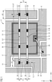
- FIG 1 shows a schematic representation of a first embodiment of a semiconductor arrangement 2 in a plan view, which comprises a first semiconductor element 4 that is contact-connected to a substrate 6.
- the first semiconductor element 4 is embodied as a vertical transistor, in particular an insulated-gate bipolar transistor (IGBT).
- IGBT insulated-gate bipolar transistor
- Further examples of such semiconductor elements are triacs, thyristors, diodes or other transistor types such as field-effect transistors or bipolar transistors.
- the IGBT comprises a control terminal, which is embodied as a gate terminal G, and load terminals, which are embodied as a collector terminal C and an emitter terminal E, wherein the collector terminal C is integrally connected to the first substrate 6 on a side of the first semiconductor element 4 facing the first substrate 6.
- the emitter terminal E has a contact surface 8, wherein the gate terminal G has a control contact surface 10 arranged electrically insulated from the contact surface 8 of the emitter terminal E.
- the contact surface 8 and the control contact surface 10 have at least one metallic layer, which may be, for example, aluminum, copper and/or gold. contains.
- the collector terminal C of the IGBT is integrally connected, for example via a soldered or sintered connection, to a first line section 12 of a substrate metallization 14 of the substrate 6.
- the substrate metallization 14 contains, for example, copper and is structured, wherein a substantially planar surface of the substrate metallization 14 defines an xy plane.
- a second line section 16 and a third line section 18 of the substrate metallization 14 are arranged on opposite sides of the first semiconductor element 4, wherein the line sections 12, 16, 18 are arranged electrically insulated from one another.
- the substrate 6 comprises a dielectric material layer 20 which contains, for example, a ceramic material, in particular aluminum nitride or aluminum oxide.
- the dielectric material layer 20 of the substrate 6 has a thickness of 25 ⁇ m to 400 ⁇ m, in particular 50 ⁇ m to 250 ⁇ m.
- the substrate 6 can be designed, among other things, as a DCB (Direct Copper Bonded) substrate.
- two wiring elements 22, 24, which are designed as bonding wires, are each electrically and mechanically connected to the second line section 16, the contact area 8 of the first semiconductor element 4, and the third line section 18, wherein a connection between the emitter E of the first semiconductor element 4 and the substrate 6 is established via the wiring elements 22, 24.
- the wiring elements 22, 24 are each connected to the second line section 16 via a first connection 26 and to the third line section 18 via a second connection 28.
- the wiring elements 22, 24 further form a plurality of chip connections 30 on the contact area 8 of the first semiconductor element 4, wherein the wiring elements 22, 24 are connected to the first semiconductor element 4 and the substrate 6 by means of ultrasonic bonding.
- the chip connections 30 to the contact area 8 of the first semiconductor element 4 are produced by looping through the respective wiring element 22, 24, in particular by means of multi-stitch wedge-to-wedge wire bonding. Multiple bonding is also called “stitching.” Such chip connections 30 are usually referred to as “stitch contacts” or “stitch bonds” and can be implemented, for example, as “wedge bonds.”
- the second line section 16 is, for example, L-shaped and, in the region of the first connections 26 of the wiring elements 22, 24, runs straight in the y-direction, so that a load current IL flows in a first current direction I1, which runs from the first connection 26 of the first wiring element 22 to the first connection 26 of the second wiring element 24.
- the first current direction I1 runs in the y-direction and thus perpendicular to the wiring elements 22, 24 arranged running in the x-direction.
- the load current IL is supplied in the x-direction before it flows straight in the y-direction in the region of the first connections 26 of the wiring elements 22, 24.
- the second line section 16 can be I-shaped, with the load current IL being supplied in the y-direction in this design.
- the third line section 18 is, for example, I-shaped and runs straight in the y-direction, so that the load current IL flows in a second current direction I2, which runs from the second connection 28 of the first wiring element 22 to the second connection 28 of the second wiring element 24.
- the second current direction I2 runs in the y-direction.
- the second current direction I2 essentially corresponds to the first current direction I1.
- the load current IL is thus supplied on one side on opposite sides via the second line section 16 and discharged via the third line section 18.
- the second line section 16 and the third line section 18 each have the same width b1, b2 Furthermore, the wiring elements 22, 24 are arranged rectilinearly in the x-direction and parallel, so that a first distance a1 between the first connections 26 on the second line section 16 and a second distance a2 between the second connections 28 on the second line section 16 are substantially equal. Thus, the line impedances between the wiring elements 22, 24 of the second line section 16 and the third line section 18 are substantially equal.
- the wiring impedances of the wiring elements 22, 24 are essentially the same, and the load current IL is distributed evenly between the two wiring elements 22, 24, for example.
- the line impedance of the second line section 16 can be adjusted, for example by varying the first width b1.
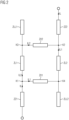
- FIG 2 shows a simplified equivalent circuit diagram of the first embodiment of the semiconductor device, which FIG 1
- the wiring impedances ZV1, ZV2 of the wiring elements 22, 24 as well as the line impedances ZL1, ZL2 of the second and third line sections 16, 18 between the respective connections of the wiring elements 22, 24 are shown.
- the supply line impedances ZZ1, ZZ2 of the first and second line sections 16, 18 as well as the no-load impedances ZLL1, ZLL2 of the no-load line sections of the second and third line sections 16, 18 are shown.
- a first node K1 is located at the point at which a first load current IL1 is branched off via the first wiring element 22, while a second load current IL2 is fed via the second line section 16 to the second wiring element 24.
- a second node K2 is located at the point where the first load current IL1 from the third line section 18 and the second load current IL2 from the second wiring element 24 are combined.
- a supply can be made analogously via the second node K2.
- the impedances can have a resistive component, in particular a series resistance, an inductive component, and/or a capacitive component.
- the load current IL flows unilaterally, i.e., via only one node K1, K2, K3, K4, and via diagonally opposite nodes K1, K2; K3, K4.
- the simplified equivalent circuit diagram results in an essentially Z-shaped current flow.
- FIG 3 shows a schematic representation of a second embodiment of a semiconductor arrangement in a plan view, wherein the contact surface 8 of the first semiconductor element 4 is connected to the second line section 16 and the third line section 18 via, for example, four wiring elements 22, 24, 32, 34 arranged rectilinearly in the x-direction and running parallel.
- the wiring elements 22, 24, 32, 34 have the same wiring diameters and substantially the same wiring lengths l.
- the distances a1, a2, a3, a4, a5, a6 between the parallel wiring elements 22, 24, 32, 34 are essentially the same size, with the second line section 16 and the third line section 18 each having the same width b1, b2 in the area of the connections 26, 28 of the wiring elements 22, 24, 32, 34.
- the further embodiment of the semiconductor device 2 in FIG 3 corresponds to the FIG 1 or FIG 2 .
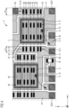
- FIG 4 shows a schematic representation of a third embodiment of a semiconductor arrangement 2 in a plan view, wherein the contact surface 8 of the first semiconductor element 4 is connected to the second line section 16 and the third line section 18 via, for example, six wiring elements 22, 24, 32, 34, 36, 38 arranged rectilinearly in the x-direction and running parallel.
- the wiring elements 22, 24, 32, 34, 36, 38 have the same wiring diameters and substantially the same wiring lengths.
- the distances between the parallel wiring elements 22, 24, 32, 34, 36, 38 are substantially the same, with the second line section 16 and the third line section 18 each having the same width b1, b2 in the region of the connections 26, 28 of the wiring elements 22, 24, 32, 34, 36, 38.
- the current IL supplied or discharged on one side is distributed evenly between the wiring elements 22, 24, 32, 34, 36, 38.
- the semiconductor arrangement 2 further comprises a second semiconductor element 40, which is connected, in particular materially, to the second line section 16 and has a contact surface 8 on a side facing away from the substrate 6.
- a fourth line section 42 and a fifth line section 44 of the substrate metallization 14 are arranged on opposite sides of the second semiconductor element 40, wherein the contact surface 8 of the second semiconductor element 40 is connected via further wiring elements 46 is connected to the fourth line section 42 and the fifth line section 44.
- the fourth line section 42 is designed to be open-circuited and is arranged directly adjacent to the second line section 16.
- the fourth line section 42 has a substantially rectangular outer contour with a narrow side 48 and a long side 50, wherein a long side 50 of the fourth line section 42 is arranged directly adjacent to the second line section 16.
- the first width b1 of the second line section 16 can be varied.
- the first line impedance ZL1 of the second line section 16 can be dimensioned by the position and/or the geometry of the fourth line section 42.
- the first semiconductor element 4 is designed as a high-side switch and the second semiconductor element 40 as a low-side switch of a half-bridge.
- the fifth line section 44 is connected to a negative DC terminal DCN of the half-bridge, while the first line section 12 is connected to a positive DC terminal DCP and the third line section 18 is connected to an AC terminal AC of the half-bridge.
- the semiconductor arrangement 2 comprises a sensor 52, in particular a temperature sensor, which is designed, for example, as an NTC thermistor (Negative Temperature Coefficient Thermistor).
- the sensor 52 is arranged in the region of the semiconductor elements 4, 40.
- the further embodiment of the semiconductor arrangement 2 in FIG 4 corresponds to the FIG 3 .
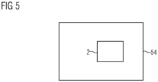
- FIG 5 shows a schematic representation of a power converter 54, which comprises, for example, a semiconductor arrangement 2.
- the invention relates to a semiconductor device 2 with a first semiconductor element 4 and a substrate 6, wherein the substrate 6 has a substrate metallization 14 with line sections 12, 16, 18, 42, 44 arranged so as to be electrically insulated from one another, wherein the first semiconductor element 4 is connected, in particular in a materially bonded manner, to a first line section 12 of the substrate metallization 14, wherein the first semiconductor element 4 has a contact surface 8 on a side facing away from the substrate 6, wherein a second line section 16 and a third line section 18 of the substrate metallization 14 are arranged on opposite sides of the first semiconductor element 4, wherein wiring elements 22, 24, 32, 34, 36, 38 are each electrically and mechanically connected to the second line section 16, the contact surface 8 of the first semiconductor element 4 and the third line section 18.
- the second line section 16 and the third line section 18 are configured such that a current IL flowing between the second line section 16 and the third line section 18 via the wiring elements 22, 24, 32, 34, 36, 38 during operation of the semiconductor device 2 flows in or out on one side on diagonally opposite sides.
Landscapes
- Semiconductor Integrated Circuits (AREA)
Priority Applications (2)
| Application Number | Priority Date | Filing Date | Title |
|---|---|---|---|
| EP23213098.9A EP4564417A1 (fr) | 2023-11-29 | 2023-11-29 | Dispositif semi-conducteur comprenant un premier élément semi-conducteur et un substrat |
| PCT/EP2024/080513 WO2025113909A1 (fr) | 2023-11-29 | 2024-10-29 | Ensemble semi-conducteur comprenant un premier élément semi-conducteur et un substrat |
Applications Claiming Priority (1)
| Application Number | Priority Date | Filing Date | Title |
|---|---|---|---|
| EP23213098.9A EP4564417A1 (fr) | 2023-11-29 | 2023-11-29 | Dispositif semi-conducteur comprenant un premier élément semi-conducteur et un substrat |
Publications (1)
| Publication Number | Publication Date |
|---|---|
| EP4564417A1 true EP4564417A1 (fr) | 2025-06-04 |
Family
ID=89029493
Family Applications (1)
| Application Number | Title | Priority Date | Filing Date |
|---|---|---|---|
| EP23213098.9A Withdrawn EP4564417A1 (fr) | 2023-11-29 | 2023-11-29 | Dispositif semi-conducteur comprenant un premier élément semi-conducteur et un substrat |
Country Status (2)
| Country | Link |
|---|---|
| EP (1) | EP4564417A1 (fr) |
| WO (1) | WO2025113909A1 (fr) |
Citations (8)
| Publication number | Priority date | Publication date | Assignee | Title |
|---|---|---|---|---|
| US20060001146A1 (en) * | 2004-06-03 | 2006-01-05 | Thomas Passe | Low inductance semiconductor device having half-bridge configuration |
| EP3226294A1 (fr) * | 2014-11-28 | 2017-10-04 | Nissan Motor Co., Ltd | Module à semi-conducteur de puissance en demi-pont et procédé pour sa fabrication |
| US20170286572A1 (en) | 2016-03-31 | 2017-10-05 | General Electric Company | Digital twin of twinned physical system |
| EP3480846A1 (fr) * | 2017-11-03 | 2019-05-08 | Infineon Technologies AG | Agencement semi-conducteur comportant des éléments à semi-conducteur commandables de façon fiable par commutation |
| US20200185359A1 (en) * | 2017-09-04 | 2020-06-11 | Mitsubishi Electric Corporation | Semiconductor module and power conversion device |
| US20200266240A1 (en) * | 2017-04-19 | 2020-08-20 | Mitsubishi Electric Corporation | Semiconductor module and power conversion apparatus |
| WO2022002464A1 (fr) | 2020-06-30 | 2022-01-06 | Siemens Aktiengesellschaft | Module de puissance comprenant au moins trois unités de puissance |
| EP4160677A1 (fr) * | 2021-09-30 | 2023-04-05 | Siemens Aktiengesellschaft | Agencement à semi-conducteurs pourvu d'au moins deux éléments semi-conducteurs |
-
2023
- 2023-11-29 EP EP23213098.9A patent/EP4564417A1/fr not_active Withdrawn
-
2024
- 2024-10-29 WO PCT/EP2024/080513 patent/WO2025113909A1/fr active Pending
Patent Citations (8)
| Publication number | Priority date | Publication date | Assignee | Title |
|---|---|---|---|---|
| US20060001146A1 (en) * | 2004-06-03 | 2006-01-05 | Thomas Passe | Low inductance semiconductor device having half-bridge configuration |
| EP3226294A1 (fr) * | 2014-11-28 | 2017-10-04 | Nissan Motor Co., Ltd | Module à semi-conducteur de puissance en demi-pont et procédé pour sa fabrication |
| US20170286572A1 (en) | 2016-03-31 | 2017-10-05 | General Electric Company | Digital twin of twinned physical system |
| US20200266240A1 (en) * | 2017-04-19 | 2020-08-20 | Mitsubishi Electric Corporation | Semiconductor module and power conversion apparatus |
| US20200185359A1 (en) * | 2017-09-04 | 2020-06-11 | Mitsubishi Electric Corporation | Semiconductor module and power conversion device |
| EP3480846A1 (fr) * | 2017-11-03 | 2019-05-08 | Infineon Technologies AG | Agencement semi-conducteur comportant des éléments à semi-conducteur commandables de façon fiable par commutation |
| WO2022002464A1 (fr) | 2020-06-30 | 2022-01-06 | Siemens Aktiengesellschaft | Module de puissance comprenant au moins trois unités de puissance |
| EP4160677A1 (fr) * | 2021-09-30 | 2023-04-05 | Siemens Aktiengesellschaft | Agencement à semi-conducteurs pourvu d'au moins deux éléments semi-conducteurs |
Also Published As
| Publication number | Publication date |
|---|---|
| WO2025113909A1 (fr) | 2025-06-05 |
Similar Documents
| Publication | Publication Date | Title |
|---|---|---|
| EP4128337B1 (fr) | Module de puissance pourvu d'au moins trois unités de puissance | |
| DE102019112935B4 (de) | Halbleitermodul | |
| EP1062698A1 (fr) | Module semi-conducteur electronique | |
| DE102020122125B4 (de) | Halbleitermodul | |
| DE102019112934A1 (de) | Halbleitermodul | |
| DE112020006374T5 (de) | Leistungsmodul mit verbesserten elektrischen und thermischen Charakteristiken | |
| DE212018000078U1 (de) | Halbleiterbauelement | |
| EP3958306A1 (fr) | Module de puissance pourvu d'au moins deux dispositifs de semi-conducteurs de puissance en contact sur un substrat | |
| EP3926670A1 (fr) | Module semi-conducteur de puissance pourvu d'au moins un élément semi-conducteur de puissance | |
| DE102019112936A1 (de) | Halbleitermodul | |
| EP4564417A1 (fr) | Dispositif semi-conducteur comprenant un premier élément semi-conducteur et un substrat | |
| WO2024022935A1 (fr) | Module semi-conducteur de puissance | |
| EP4367717A1 (fr) | Ensemble semi-conducteur comprenant au moins deux éléments semi-conducteurs | |
| DE102006002381B3 (de) | Leistungshalbleiterbauteil mit Chipstapel und Verfahren zu seiner Herstellung | |
| EP4120341A1 (fr) | Agencement de semi-conducteur doté d'un élément semi-conducteur, d'un substrat et des moyens de liaison par soudage | |
| DE212022000168U1 (de) | Leistungsmodul | |
| EP4030604A1 (fr) | Convertisseur pourvu d'au moins deux modules de semi-conducteur de puissance | |
| DE102022118114B4 (de) | Halbleitervorrichtung | |
| EP4312263A1 (fr) | Dispositif semi-conducteur doté d'un élément semi-conducteur, d'un substrat et d'au moins un élément de câblage | |
| EP4546408A1 (fr) | Dispositif semi-conducteur comprenant un premier élément semi-conducteur | |
| EP4665089A1 (fr) | Agencement de circuit | |
| DE102010001788A1 (de) | Skalierbarer Aufbau für laterale Halbleiterbauelemente mit hoher Stromtragfähigkeit | |
| EP4576211A1 (fr) | Module semi-conducteur comprenant un circuit semi-conducteur et un boîtier | |
| EP4533540A1 (fr) | Module de puissance, onduleur comprenant un module de puissance | |
| EP4495989A1 (fr) | Dispositif semi-conducteur comprenant un élément semi-conducteur |
Legal Events
| Date | Code | Title | Description |
|---|---|---|---|
| PUAI | Public reference made under article 153(3) epc to a published international application that has entered the european phase |
Free format text: ORIGINAL CODE: 0009012 |
|
| STAA | Information on the status of an ep patent application or granted ep patent |
Free format text: STATUS: THE APPLICATION HAS BEEN PUBLISHED |
|
| AK | Designated contracting states |
Kind code of ref document: A1 Designated state(s): AL AT BE BG CH CY CZ DE DK EE ES FI FR GB GR HR HU IE IS IT LI LT LU LV MC ME MK MT NL NO PL PT RO RS SE SI SK SM TR |
|
| STAA | Information on the status of an ep patent application or granted ep patent |
Free format text: STATUS: THE APPLICATION IS DEEMED TO BE WITHDRAWN |
|
| 18D | Application deemed to be withdrawn |
Effective date: 20251205 |