EP4009375B1 - Leistungshalbleiterbauelement und herstellungsverfahren zur herstellung eines leistungshalbleiterbauelements - Google Patents
Leistungshalbleiterbauelement und herstellungsverfahren zur herstellung eines leistungshalbleiterbauelements Download PDFInfo
- Publication number
- EP4009375B1 EP4009375B1 EP20211565.5A EP20211565A EP4009375B1 EP 4009375 B1 EP4009375 B1 EP 4009375B1 EP 20211565 A EP20211565 A EP 20211565A EP 4009375 B1 EP4009375 B1 EP 4009375B1
- Authority
- EP
- European Patent Office
- Prior art keywords
- layer
- base layer
- zone
- contact
- semiconductor device
- Prior art date
- Legal status (The legal status is an assumption and is not a legal conclusion. Google has not performed a legal analysis and makes no representation as to the accuracy of the status listed.)
- Active
Links
Images


Classifications
-
- H—ELECTRICITY
- H10—SEMICONDUCTOR DEVICES; ELECTRIC SOLID-STATE DEVICES NOT OTHERWISE PROVIDED FOR
- H10D—INORGANIC ELECTRIC SEMICONDUCTOR DEVICES
- H10D62/00—Semiconductor bodies, or regions thereof, of devices having potential barriers
- H10D62/10—Shapes, relative sizes or dispositions of the regions of the semiconductor bodies; Shapes of the semiconductor bodies
- H10D62/102—Constructional design considerations for preventing surface leakage or controlling electric field concentration
- H10D62/103—Constructional design considerations for preventing surface leakage or controlling electric field concentration for increasing or controlling the breakdown voltage of reverse-biased devices
- H10D62/105—Constructional design considerations for preventing surface leakage or controlling electric field concentration for increasing or controlling the breakdown voltage of reverse-biased devices by having particular doping profiles, shapes or arrangements of PN junctions; by having supplementary regions, e.g. junction termination extension [JTE]
- H10D62/106—Constructional design considerations for preventing surface leakage or controlling electric field concentration for increasing or controlling the breakdown voltage of reverse-biased devices by having particular doping profiles, shapes or arrangements of PN junctions; by having supplementary regions, e.g. junction termination extension [JTE] having supplementary regions doped oppositely to or in rectifying contact with regions of the semiconductor bodies, e.g. guard rings with PN or Schottky junctions
- H10D62/107—Buried supplementary regions, e.g. buried guard rings
-
- H—ELECTRICITY
- H10—SEMICONDUCTOR DEVICES; ELECTRIC SOLID-STATE DEVICES NOT OTHERWISE PROVIDED FOR
- H10D—INORGANIC ELECTRIC SEMICONDUCTOR DEVICES
- H10D62/00—Semiconductor bodies, or regions thereof, of devices having potential barriers
- H10D62/10—Shapes, relative sizes or dispositions of the regions of the semiconductor bodies; Shapes of the semiconductor bodies
- H10D62/102—Constructional design considerations for preventing surface leakage or controlling electric field concentration
- H10D62/103—Constructional design considerations for preventing surface leakage or controlling electric field concentration for increasing or controlling the breakdown voltage of reverse-biased devices
- H10D62/105—Constructional design considerations for preventing surface leakage or controlling electric field concentration for increasing or controlling the breakdown voltage of reverse-biased devices by having particular doping profiles, shapes or arrangements of PN junctions; by having supplementary regions, e.g. junction termination extension [JTE]
- H10D62/109—Reduced surface field [RESURF] PN junction structures
- H10D62/111—Multiple RESURF structures, e.g. double RESURF or 3D-RESURF structures
-
- H—ELECTRICITY
- H10—SEMICONDUCTOR DEVICES; ELECTRIC SOLID-STATE DEVICES NOT OTHERWISE PROVIDED FOR
- H10D—INORGANIC ELECTRIC SEMICONDUCTOR DEVICES
- H10D12/00—Bipolar devices controlled by the field effect, e.g. insulated-gate bipolar transistors [IGBT]
- H10D12/01—Manufacture or treatment
- H10D12/031—Manufacture or treatment of IGBTs
-
- H—ELECTRICITY
- H10—SEMICONDUCTOR DEVICES; ELECTRIC SOLID-STATE DEVICES NOT OTHERWISE PROVIDED FOR
- H10D—INORGANIC ELECTRIC SEMICONDUCTOR DEVICES
- H10D12/00—Bipolar devices controlled by the field effect, e.g. insulated-gate bipolar transistors [IGBT]
- H10D12/411—Insulated-gate bipolar transistors [IGBT]
- H10D12/441—Vertical IGBTs
-
- H—ELECTRICITY
- H10—SEMICONDUCTOR DEVICES; ELECTRIC SOLID-STATE DEVICES NOT OTHERWISE PROVIDED FOR
- H10D—INORGANIC ELECTRIC SEMICONDUCTOR DEVICES
- H10D30/00—Field-effect transistors [FET]
- H10D30/60—Insulated-gate field-effect transistors [IGFET]
- H10D30/64—Double-diffused metal-oxide semiconductor [DMOS] FETs
- H10D30/66—Vertical DMOS [VDMOS] FETs
-
- H—ELECTRICITY
- H10—SEMICONDUCTOR DEVICES; ELECTRIC SOLID-STATE DEVICES NOT OTHERWISE PROVIDED FOR
- H10D—INORGANIC ELECTRIC SEMICONDUCTOR DEVICES
- H10D62/00—Semiconductor bodies, or regions thereof, of devices having potential barriers
- H10D62/10—Shapes, relative sizes or dispositions of the regions of the semiconductor bodies; Shapes of the semiconductor bodies
- H10D62/17—Semiconductor regions connected to electrodes not carrying current to be rectified, amplified or switched, e.g. channel regions
- H10D62/393—Body regions of DMOS transistors or IGBTs
-
- H—ELECTRICITY
- H10—SEMICONDUCTOR DEVICES; ELECTRIC SOLID-STATE DEVICES NOT OTHERWISE PROVIDED FOR
- H10D—INORGANIC ELECTRIC SEMICONDUCTOR DEVICES
- H10D62/00—Semiconductor bodies, or regions thereof, of devices having potential barriers
- H10D62/80—Semiconductor bodies, or regions thereof, of devices having potential barriers characterised by the materials
- H10D62/83—Semiconductor bodies, or regions thereof, of devices having potential barriers characterised by the materials being Group IV materials, e.g. B-doped Si or undoped Ge
- H10D62/832—Semiconductor bodies, or regions thereof, of devices having potential barriers characterised by the materials being Group IV materials, e.g. B-doped Si or undoped Ge being Group IV materials comprising two or more elements, e.g. SiGe
- H10D62/8325—Silicon carbide
-
- H—ELECTRICITY
- H10—SEMICONDUCTOR DEVICES; ELECTRIC SOLID-STATE DEVICES NOT OTHERWISE PROVIDED FOR
- H10D—INORGANIC ELECTRIC SEMICONDUCTOR DEVICES
- H10D64/00—Electrodes of devices having potential barriers
- H10D64/20—Electrodes characterised by their shapes, relative sizes or dispositions
- H10D64/23—Electrodes carrying the current to be rectified, amplified, oscillated or switched, e.g. sources, drains, anodes or cathodes
- H10D64/251—Source or drain electrodes for field-effect devices
- H10D64/252—Source or drain electrodes for field-effect devices for vertical or pseudo-vertical devices
-
- H—ELECTRICITY
- H10—SEMICONDUCTOR DEVICES; ELECTRIC SOLID-STATE DEVICES NOT OTHERWISE PROVIDED FOR
- H10D—INORGANIC ELECTRIC SEMICONDUCTOR DEVICES
- H10D64/00—Electrodes of devices having potential barriers
- H10D64/20—Electrodes characterised by their shapes, relative sizes or dispositions
- H10D64/23—Electrodes carrying the current to be rectified, amplified, oscillated or switched, e.g. sources, drains, anodes or cathodes
- H10D64/251—Source or drain electrodes for field-effect devices
- H10D64/258—Source or drain electrodes for field-effect devices characterised by the relative positions of the source or drain electrodes with respect to the gate electrode
-
- H—ELECTRICITY
- H10—SEMICONDUCTOR DEVICES; ELECTRIC SOLID-STATE DEVICES NOT OTHERWISE PROVIDED FOR
- H10P—GENERIC PROCESSES OR APPARATUS FOR THE MANUFACTURE OR TREATMENT OF DEVICES COVERED BY CLASS H10
- H10P30/00—Ion implantation into wafers, substrates or parts of devices
- H10P30/20—Ion implantation into wafers, substrates or parts of devices into semiconductor materials, e.g. for doping
- H10P30/202—Ion implantation into wafers, substrates or parts of devices into semiconductor materials, e.g. for doping characterised by the semiconductor materials
- H10P30/204—Ion implantation into wafers, substrates or parts of devices into semiconductor materials, e.g. for doping characterised by the semiconductor materials into Group IV semiconductors
- H10P30/2042—Ion implantation into wafers, substrates or parts of devices into semiconductor materials, e.g. for doping characterised by the semiconductor materials into Group IV semiconductors into crystalline silicon carbide
-
- H—ELECTRICITY
- H10—SEMICONDUCTOR DEVICES; ELECTRIC SOLID-STATE DEVICES NOT OTHERWISE PROVIDED FOR
- H10P—GENERIC PROCESSES OR APPARATUS FOR THE MANUFACTURE OR TREATMENT OF DEVICES COVERED BY CLASS H10
- H10P30/00—Ion implantation into wafers, substrates or parts of devices
- H10P30/20—Ion implantation into wafers, substrates or parts of devices into semiconductor materials, e.g. for doping
- H10P30/21—Ion implantation into wafers, substrates or parts of devices into semiconductor materials, e.g. for doping of electrically active species
Definitions
- the invention relates to a power semiconductor device and a method for producing a power semiconductor device.
- Schottky power semiconductor devices e.g. metal oxide semiconductor field effect transistor (MOSFET) devices or insulated-gate bipolar transistor (IGBT) devices, offering excellent overall performance both for static and dynamic electrical parameters.
- MOSFET metal oxide semiconductor field effect transistor
- IGBT insulated-gate bipolar transistor
- Schottky MOSFET devices do not feature doped contact regions or well regions, e.g. n+ doped contacts or p+ doped wells. This is to say that such Schottky power semiconductor devices do not have a metallurgical junction to protect a gate oxide.
- Document US 6 091 108 A relates to a semiconductor device of SiC having an insulated gate and buried grid region for high breakdown voltage.
- Document US 5 962 893 A relates to a Schottky tunneling device.
- Document US 2018/308938 A1 relates to a SiC semiconductor device with offset in trench bottom.
- Document US 2014/183553 A1 relates to transistor structures, having a reduced electrical field at the gate oxide and methods for making such transistor structures.
- Document EP 3 255 676 A1 relates to a vertical power semiconductor device and a method for operating such a device.
- document EP 3 255 676 A1 a MOSFET is described comprising a protection layer, which is p-doped, and which is in contact with the insulation layer, wherein a maximum doping concentration of the p-doped layer is larger than 10 18 1/cm 3 . It is an object of the invention to provide a power semiconductor device, which has an improved reliability and to provide a method for producing such a power semiconductor device.
- a first aspect of the invention relates to a power semiconductor device as defined in claim 1.
- the power semiconductor device is, for example a power MOSFET or a power IGBT. Further, the power semiconductor device is, for example, a Schottky power semiconductor device.
- the power semiconductor device is based, for example, on silicon carbide. This is to say that the power semiconductor device is, for example, either a SiC power MOSFET or a SiC power IGBT.
- the power semiconductor device comprises an electrode.
- the electrode can comprise, for example a metal or consists of a metal.
- the electrode is an electrode being externally contactable in an electrical conductive manner.
- the electrode has, for example, a main plain of extension. Lateral directions are aligned parallel to the main plain of extension, and a vertical direction is aligned perpendicular to the main plain of extension.
- the power semiconductor device comprises a base layer of a first conductivity type provided on the electrode.
- the base layer for example, comprises a semiconductor material or consists of a semiconductor material.
- the base layer is an epitaxial base layer.
- the base layer comprises Silicon Carbide (SiC), for example.
- SiC Silicon Carbide
- Silicon carbide is a chemical compound of silicon and carbon belonging to the group of carbides. Silicon carbide is a polytype material, wherein some polytypes have a band gap of up to 3.33 eV, such as 2H-SiC, making SiC a semiconductor with a wide band gap.
- the base layer comprises, for example n-type dopants such that the first conductivity type is an n-type conductivity.
- a doping concentration of the first dopants of the base layer can be homogeneous. Alternatively, the doping concentration can increase towards the electrode or the doping concentration has a region of higher doping concentration at the electrode.
- the base layer is, for example, in direct contact to the electrode or if between the base layer and the electrode no layer of a second conductivity type is provided, the power semiconductor device is a power MOSFET.
- an injecting layer of the second conductivity type is provided on the base layer.
- the injecting layer is arranged between the base layer and the electrode.
- the power semiconductor device is, for example, a power IGBT.
- the injecting layer comprises p-type dopants such that the second conductivity type is a p-type conductivity.
- the first conductivity type and the second conductivity type can be inversed.
- the power semiconductor device comprises at least one contact layer provided on the base layer.
- the contact layer is arranged on a top surface of the base layer, facing away from the electrode.
- the contact layer has, for example a main extension direction in lateral directions.
- the contact layer is, for example, externally contactable in an electrical conductive manner.
- At least two contact layers are provided on the base layer.
- the contact layers are spaced apart from one another.
- the main extension directions of the contact layers extend parallel to one another.
- One of the at least two contact layers is formed, e.g., as a source of the power MOSFET and the other one of the at least two contact layers is formed, e.g., as a drain of the power MOSFET.
- the power semiconductor device comprises a gate contact provided on the base layer and on the contact layer.
- the gate contact has a main extension direction being parallel to the lateral directions, for example.
- the main extension direction of the gate contact extends, for example, perpendicular to the main extension directions of the contact layer.
- the gate contact comprises or consists of at least one of a metal and polysilicon, for example. Further, the gate contact is, at least in regions, externally contactable in an electrical conductive manner.
- the power semiconductor device comprises an insulation layer between the gate contact and the base layer and between the contact layer and the gate contact.
- the gate layer is embedded in the insulation layer. This is to say that the insulation layer covers all outer surfaces of the gate contact, except the region for externally contacting.
- the insulation layer comprises, for example, a dielectric material.
- the insulation layer is a gate oxide, for example.
- the insulation layer includes high K dielectric stacks. In this case, the k dielectric stacks comprise or consist of materials with a higher relative permittivity than silicon dioxide, so-called high-K materials.
- the power semiconductor device comprises at least one zone of a second conductivity type different from the first conductivity type within the base layer.
- the zone is embedded within the base layer.
- embedded can mean that a top surface, a bottom surface and at least two side surfaces of the zone is covered by the base layer.
- Embedded means that an outer surface of the zone is completely covered by the base layer, such that the zone is completely enclosed by the base layer in a three dimensional manner.
- the zone can have a triangular, a squared, a rectangular, a round, an oval or an elliptic form in a cross section along one of the lateral directions and the vertical direction.
- the zone comprises, for example p-type dopants such that the second conductivity type is a p-type conductivity.
- the zone comprises n-type dopants such that the second conductivity type is an n-type conductivity.
- the second conductivity type is different from the first conductivity type. This is to say if the base layer comprises n-type dopants the zone comprises p-type dopants and vice versa.
- the at least one zone shifts away a peak electric field generated in the base layer from the insulation layer between the gate contact and the base layer.
- the peak electric field is an electrical field, which, for example, at least one of temporarily and locally strongly increases or decreases.
- electric field is a combination of two exponential parts, one exponentially increasing part and another exponentially decreasing part.
- the at least one zone of the second conductivity type is shaped and arranged such that the zone shifts away the peak electric field produced in the base layer from the interface between the insulation layer of the gate contact and a region of the base layer facing the gate contact.
- the at least one contact layer is a metallic layer.
- the metallic layers comprise a metal or consist of a metal.
- An interface between the metallic layer and the base layer forms a Schottky contact.
- a material composition such as a doping concentration of the base layer and a work function of the metallic layer, is selected such that a depletion zone is formed in a region of the interface within the base layer.
- the at least one contact layer comprises or consists of a semiconductor material having a first region of the first conductivity and a second region of the second conductivity.
- the first region is configured for external contacting.
- the second region is arranged between the first region and the drift layer.
- the base layer comprises a plain top surface and the at least one metallic layer does not extend into the base layer in vertical direction.
- the top surface faces away from the electrode. This is to say that the metallic layer and the base layer do not overlap with one another in vertical direction. In this way, the contact does not require expensive implantation and activation steps.
- the base layer comprises at least one recessed top surface and the at least one contact layer is provided on the at least one recessed top surface.
- the base layer comprises a bar structure facing away from the electrode.
- the bar structure comprises a top surface and at least one side surface.
- the side surface connects the top surface of the bar structure with the recessed top surface of the base layer.
- the bar structure extends, exemplarily along a main extension direction in lateral directions being perpendicular to the main extension direction of the gate contact. Further, the bar structure is arranged in a central position of the base layer.
- the bar structure and the base layer are formed in one piece. This is to say that the bar structure is a part of the base layer. According to this embodiment, the contact layer and the base layer overlap with one another in vertical direction.
- At least one of the gate contact and the insulation layer partially overlaps with the at least one contact layer in lateral directions.
- an overlap of the at least one of the gate contact and the insulation layer in lateral directions with the at least one contact layer is between at least 0.001 ⁇ m and at most 3 ⁇ m.
- the overlap of the at least one of the gate contact and the insulation layer in lateral directions with the at least one contact layer is between at least 0.2 ⁇ m and at most 2 ⁇ m.
- the at least one zone is provided centred in lateral directions with respect to the gate contact.
- the zone is arranged centred between the contact layers in lateral directions. If there is only a single zone, the zone has equal distances to the contact layers in lateral directions.
- a centred arrangement of the zone exemplarily improves the controllability of the electric field within the base layer such that the electric field can then extend symmetrically within the base layer.
- the at least one zone has a main extension direction in lateral directions transverse to a main extension direction of the base layer in lateral directions.
- the main extension direction of the zone is perpendicular to the main extension direction of the base layer in lateral directions.
- the at least one zone has a length in lateral directions being equal to the length of the at least one contact layer.
- the length of the at least one zone is, for example, an extend of the zone in lateral directions along the main extension direction of the zone.
- the length of the contact layer is, for example, an extend of the contact layer in lateral directions along the main extension direction of the contact layer. E.g. the main extension direction of the contact layers is parallel to the main extension direction of the zone.
- the length of the zone is equal to a width of at least one of the gate contact and the insulation layer, for example.
- the width of at least one of the gate contact and the insulation layer is, for example, an extend of at least one of the gate contact and the insulation layer in lateral directions perpendicular to the main extension direction of at least one of the gate contact and the insulation layer.
- the device can have an improved resistance such that the resistance of the device is sufficiently low.
- a distance between the zone and the insulation layer is at most 1 ⁇ m.
- the distance is the minimal distance in vertical direction between the zone and the insulation layer. It is possible that the zone and the insulation layer can be in direct contact with one another. Further, the distance between the zone and the insulation layer is at most 0.25 ⁇ m, for example.
- the at least one zone comprises a peak doping concentration being at least 10 15 1/cm 3 and at most 5 ⁇ 10 17 1/cm 3 .
- a doping concentration of the zone has a maximum value being the peak doping concentration value within the zone.
- the at least one zone comprises a peak doping concentration being up to one hundred times higher than a peak doping concentration of the base layer.
- a thickness of the at least one zone is at least 0.1 ⁇ m and at most 1 ⁇ m.
- the thickness is the minimal extension in vertical direction of the zone.
- the thickness of the zone is, for example at least 0.2 ⁇ m and at most 0.6 ⁇ m.
- the at least one zone has a width in lateral directions along a main extension direction of the base layer, which is less than 40 % of a length of the gate contact in lateral directions along the main extension direction of the base layer.
- the main extension direction of the base layer equals a main extension direction of the gate contact. If the zone has a width being larger than 40 % of the length of the gate contact, a current flow through the base layer is hindered and significantly increase an on-state resistance. Due to such a width of less than 40 %, the on-state resistance increase is negligible.
- the power semiconductor device comprises at least two zones of the second conductivity type, wherein the at least two zones are provided in a common plane extending in lateral directions.
- the power semiconductor device comprises at least three zones of the second conductivity type.
- the at least three zones form a retrograde profile in a cross sectional view perpendicular to lateral directions.
- the retrograde profile is a doping profile, wherein a peak doping concentration of the doping profile faces away from the contact layer.
- a peak doping concentration of the retrograde profile faces away from the gate contact.
- the peak is located in the centre between the contact layers.
- a zone in a region of the peak is arranged further away from the gate contact in vertical direction than a zone in regions not located at the peak.
- the zones not located at the peak are arranged symmetrically around the zone in the region of the peak.
- the zones can be arranged on grid points of a regular grid.
- the grid for example, is a triangular, rectangular or hexagonal grid.
- a so-called a dead zone for the current is located around each zone. Due to diffusion, such a dead zone is, e.g., smaller than the respective zone.
- a plurality of zones being smaller than a single zone can spread the current better than the single zone being larger than the plurality of zones.
- a second aspect of the invention relates to a method for producing a power semiconductor device as defined in claim 10.
- the method produces a power semiconductor device described herein above. All features disclosed in connection with the power semiconductor device are therefore also disclosed in connection with the method and vice versa.
- an electrode is provided.
- a base layer of a first conductivity type is provided on the electrode.
- At least one contact layer is applied on the base layer.
- a gate contact and an insulation layer are applied on the base layer and at least one contact layer, wherein the insulation layer is applied between the gate contact and the base layer and between the at least one contact layer and the gate contact.
- At least one zone of a second conductivity type different from the first conductivity type is generated within the base layer, wherein the at least one zone is constructed and arranged to shift away a peak electric field generated in the base layer from the insulation layer between the gate contact and the base layer.
- the zone is generated by implanting dopants of the second conductivity type within the base layer.
- a material of the base layer is grown on top of the generated zone and the adjacent base layer, for example. Due to such an overgrowth process, the zone can be embedded within the base layer.
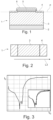
- the MOSFET according to the prior art in Figure 1 comprises an electrode 2, a base layer 3 being arranged on the electrode 2, two contact layers 4 being arranged on the base layer 3, a gate contact 5 being arranged on the base layer 3, and an insulation layer 6 between the gate contact 5 and the base layer 3.
- FIG. 2 a cross-section P, marked in Figure 1 , through the contact layers 4 and the base layer 3 is shown. Further, a main extension direction of the base layer L3 in lateral directions is depicted in Figure 2 .
- the current-voltage characteristic of Figure 3 shows a drain current Id for different gate voltages Vg of the MOSFET according to the prior art according to Figures 1 and 2 .
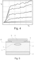
- the current-voltage characteristic of Figure 5 shows a drain current Id for different drain voltages Vd of the MOSFET according to the prior art according to Figures 1 and 2 .
- the power semiconductor device 1 comprises an electrode 2 on which a base layer 3 of a first conductivity type is provided. A top surface of the base layer 3 is plain. On this plain top surface of the base layer 3, two contact layers 4, each being a metallic layer, are arranged. In a side view of the power semiconductor device 1, the metallic layers and the base layer 3 do not overlap with one another.
- a gate contact 5 is provided on the base layer 3 and on the metallic layers.
- the gate contact 5 is enclosed by an insulation layer 6, except the region for externally contacting.
- the insulation layer 6 is arranged between the gate contact 5 and the base layer 3 as well as between the at least two metallic layers and the gate contact 5.
- the gate contact 5 and the insulation layer 6 partially overlap in lateral directions with the metallic layers.
- An overlap of the gate contact 5 and the insulation layer 6 with each of the metallic layers is, for example, is at least 0.2 ⁇ m and at most 2 ⁇ m. Furthermore, a side surface of each of the metallic layers are completely covered by the insulation layer 6.
- a zone 7 of a second conductivity type is located within the base layer 3.
- an outer surface of the zone 7 is completely covered by the base layer 3 such that the zone 7 is completely enclosed by the base layer 3 in two dimensions.
- the zone 7 is provided centred in lateral directions with respect to the gate contact 5. For example, a distance between the zone 7 and the insulation layer 6 is at most 1 ⁇ m.
- the base layer 3 of the first conductivity type comprises n-type dopants.
- the zone 7 of a second conductivity type comprises p-type dopants. Due to such an arrangement of the zone 7 of the second conductivity type, a peak electric field generated in the base layer 3 is shifted away from the insulation layer 6 between the gate contact 5 and the base layer 3.
- a simulation a doping profile according to Figure 6 corresponds to a MOSFET according to Figures 1 and 2 without having a zone 7 of the second conductivity type.
- Simulations of doping profiles of the Figures 7 and 8 correspond to a power semiconductor device 1 with a zone 7 of a second conductivity type according to the embodiment of Figure 5 .
- a doping concentration is represented by shaded areas.
- shaded areas with a comparatively high density of lines corresponds to a comparatively high doping concentration. Consequently, shaded areas with a comparatively low density of lines corresponds to a comparatively low doping concentration.
- the zone 7 of the second conductivity comprises a peak doping concentration being at least 10 15 1/cm 3 and at most 5 ⁇ 10 17 1/cm 3 corresponding to the shaded area with the highest density of lines.
- a simulation of an electric field profile according to Figure 9 is based on the simulated doping profile according to Figure 6 .
- an absolute value of an electric field in V/cm is about 1.7 ⁇ 10 6 V/cm directly below the gate contact 5 in a first region.
- An electric field of a second region, adjacent to the first region, is about 1.6 ⁇ 10 6 V/cm.
- a simulation of an electric current density according to Figure 12 is based on the simulated doping profile according to Figure 6 .
- the simulations of the electric current density according to Figures 13 and 14 are based on the doping profiles of Figures 7 and 8 , respectively.
- the electric current density below directly below the gate contact 5 in a first region is less for the power semiconductor device 1 according to Figure 13 and 14 .
- a density of lines of shown shaded areas correspond to a value of the electric current density.
- the base body of the power semiconductor device 1 comprise in contrast to the embodiment in connection with Figure 5 a bar structure.
- the bar structure and the base body are formed in one piece. Due to the bar structure, the base body comprises two recessed top surfaces. On each of the two recessed top surfaces one contact layer 4 is arranged.
- an injecting layer 8 of the second conductivity type is arranged between the electrode 2 and the base layer 3.
- the power semiconductor device 1 is an IGBT.
- the zone 7 has a main extension direction L7 in lateral directions being perpendicular to a main extension direction of the base layer L3. Furthermore, the zone 7 has a width in lateral directions along the main extension direction of the base layer L3, which is less than 40 % of a length of the gate contact 5 in lateral directions along the main extension direction of the base layer L3.
- the zone 7 being arranged centred between the two contact layers 4 in lateral directions extend along the main extension direction of the zone L7 over the whole width of the base layer 3 along the main extension direction of the zone L7.
- the base layer 3 according to Figures 17 and 18 comprises three zones 7.
- the zones 7 are arranged spaced apart from one another. Furthermore, the main extension directions of the zones L7 are running parallel to one another. In this embodiment, the zones 7 are arranged in a common plane. This is to say that each zone 7 has a same minimal distant to the gate contact 5.
- the three zones 7 according to Figures 19 and 20 form a retrograde profile in a cross sectional view perpendicular to lateral directions.
- the retrograde profile comprises a peak facing away from the gate contact 5.
- the zone 7 in the middle of the three zones 7 has a minimal distance to the gate contact 5 in vertical direction than the outer two zones 7.
- the power semiconductor device 1 comprises five zones 7.
- Each zone 7 does is formed of a square in plan view. In this embodiment, each zone 7 does not extend over the whole width of the base layer 3. Rather, each zones 7 forms a single pocket within the base layer 3 being completely, e.g. three dimensionally, surrounded by the base layer 3.
- One of the zones 7 is arranged in centred with respect to the gate contact 5 in lateral directions.
- Four of the five zones 7 are arranged symmetrically around the zone 7 arranged centred. These four zones 7 are arranged on grid points of a rectangular grid, e.g. in a box-like fashion.
- an electrode 2 is provided and, in the method step 200, a base layer 3 of a first conductivity type is provided on the electrode 2.
- a next method step 300 at least two contact layers 4 are applied on the base layer 3.
- a gate contact 5 and an insulation layer 6 are applied on the base layer 3 and at least two contact layers 4, wherein the insulation layer 6 is applied between the gate contact 5 and the base layer 3 and between the at least two contact layers 4 and the gate contact 5
- At least one zone 7 of a second conductivity type is generated within the base layer 3, wherein the at least one zone 7 is constructed and arranged to shift away a peak electric field generated in the base layer 3 from the insulation layer 6 between the gate contact 5 and the base layer 3.
Landscapes
- Electrodes Of Semiconductors (AREA)
- Chemical & Material Sciences (AREA)
- Composite Materials (AREA)
- Junction Field-Effect Transistors (AREA)
Claims (10)
- Leistungshalbleitervorrichtung (1), die Folgendes umfasst:- eine Elektrode (2);- eine auf der Elektrode (2) bereitgestellte Basisschicht (3) eines ersten Leitfähigkeitstyps;- mindestens eine auf der Basisschicht (3) bereitgestellte Kontaktschicht (4);- einen auf der Basisschicht (3) und auf der mindestens einen Kontaktschicht (4) bereitgestellten Gate-Kontakt (5);- eine Isolationsschicht (6) zwischen dem Gate-Kontakt (5) und der Basisschicht (3) sowie zwischen der mindestens einen Kontaktschicht (4) und dem Gate-Kontakt (5) und- mindestens eine Zone (7) eines zweiten Leitfähigkeitstyps, der sich von dem ersten Leitfähigkeitstyp unterscheidet, in der Basisschicht (3),- wobei die mindestens eine Kontaktschicht (4) auf einer von der Elektrode (2) abgewandten Oberseite der Basisschicht (3) angeordnet ist,- wobei die mindestens eine Kontaktschicht (4) eine metallische Schicht ist,- wobei eine Grenzfläche zwischen der metallischen Schicht und der Basisschicht (3) einen Schottky-Kontakt bildet,- wobei die mindestens eine Zone (7) in der Basisschicht (3) so eingebettet ist, dass eine äußere Oberfläche der Zone (7) vollständig von der Basisschicht (3) bedeckt ist und dass die mindestens eine Zone (7) vollständig dreidimensional von der Basisschicht (3) umschlossen ist,- wobei die mindestens eine Zone (7) in seitlichen Richtungen in Bezug auf den Gate-Kontakt (5) zentriert bereitgestellt ist und ein Abstand zwischen der mindestens einen Zone (7) und der Isolationsschicht (6) höchstens 1 µm beträgt,- wobei die mindestens eine Zone (7) eine Spitzendotierungskonzentration von mindestens 1015 1/cm3 und höchstens 5×10¹⁷ 1/cm3 umfasst und- wobei die mindestens eine Zone (7) ein in der Basisschicht (3) erzeugtes elektrisches Spitzenfeld von der Isolationsschicht (6) zwischen dem Gate-Kontakt (5) und der Basisschicht (3) weg verschiebt.
- Leistungshalbleitervorrichtung (1) nach dem vorhergehenden Anspruch, wobei- die Basisschicht (3) eine ebene Oberseite aufweist und sich die mindestens eine metallische Schicht in vertikaler Richtung nicht in die Basisschicht (3) erstreckt oder- die Basisschicht (3) mindestens eine vertiefte Oberseite umfasst und die mindestens eine Kontaktschicht (4) auf der mindestens einen vertieften Oberseite bereitgestellt ist.
- Leistungshalbleitervorrichtung (1) nach einem der vorhergehenden Ansprüche, wobei sich der Gate-Kontakt (5) und/oder die Isolationsschicht (6) in seitlichen Richtungen teilweise mit der mindestens einen Kontaktschicht (4) überlappt.
- Leistungshalbleitervorrichtung (1) nach Anspruch 3, wobei die Überlappung des Gate-Kontakts (5) und/oder der Isolationsschicht (6) in seitlichen Richtungen mit der mindestens einen Kontaktschicht (4) mindestens 0,001 µm und höchstens 3 µm beträgt.
- Leistungshalbleitervorrichtung (1) nach einem der vorhergehenden Ansprüche, wobei die mindestens eine Zone (7) eine Haupterstreckungsrichtung (L7) in seitlichen Richtungen quer zu einer Haupterstreckungsrichtung der Basisschicht (L3) in seitlichen Richtungen aufweist.
- Leistungshalbleitervorrichtung (1) nach dem vorhergehenden Anspruch, wobei die mindestens eine Zone (7) eine Länge in seitlichen Richtungen aufweist, die gleich einer Länge der mindestens einen Kontaktschicht (4) ist.
- Leistungshalbleitervorrichtung (1) nach einem der vorhergehenden Ansprüche, wobei die mindestens eine Zone (7) eine Spitzendotierungskonzentration umfasst, die bis zu hundertmal höher als eine Spitzendotierungskonzentration der Basisschicht (3) ist.
- Leistungshalbleitervorrichtung (1) nach einem der vorhergehenden Ansprüche, wobei eine Dicke der mindestens einen Zone (7) mindestens 0,1 µm und höchstens 1 µm beträgt.
- Leistungshalbleitervorrichtung (1) nach einem der vorhergehenden Ansprüche, wobei die mindestens eine Zone (7) in seitlichen Richtungen entlang einer Haupterstreckungsrichtung der Basisschicht (L3) eine Breite aufweist, die weniger als 40 % einer Länge des Gate-Kontakts (5) in seitlichen Richtungen entlang der Haupterstreckungsrichtung der Basisschicht (L3) beträgt.
- Verfahren zur Herstellung einer Leistungshalbleitervorrichtung (1), das die folgenden Schritte umfasst:Bereitstellen (100) einer Elektrode (2);Bereitstellen (200) einer Basisschicht (3) eines ersten Leitfähigkeitstyps auf der Elektrode (2);Aufbringen (300) mindestens einer Kontaktschicht (4) auf der Basisschicht (3);Aufbringen (400) eines Gate-Kontakts (5) und einer Isolationsschicht (6) auf der Basisschicht (3) und der mindestens einen Kontaktschicht (4), wobei die Isolationsschicht (6) zwischen dem Gate-Kontakt (5) und der Basisschicht (3) sowie zwischen der mindestens einen Kontaktschicht (4) und dem Gate-Kontakt (5) aufgebracht wird, und Erzeugen (500) mindestens einer Zone (7) eines zweiten Leitfähigkeitstyps, der sich von dem ersten Leitfähigkeitstyp unterscheidet, in der Basisschicht (3),- wobei die mindestens eine Kontaktschicht (4) auf einer von der Elektrode (2) abgewandten Oberseite der Basisschicht (3) angeordnet ist,- wobei die mindestens eine Kontaktschicht (4) eine metallische Schicht ist,- wobei eine Grenzfläche zwischen der metallischen Schicht und der Basisschicht (3) einen Schottky-Kontakt bildet,- wobei die mindestens eine Zone (7) in der Basisschicht (3) so eingebettet ist, dass eine äußere Oberfläche der Zone (7) vollständig von der Basisschicht (3) bedeckt ist und dass die mindestens eine Zone (7) vollständig dreidimensional von der Basisschicht (3) umschlossen ist,- wobei die mindestens eine Zone (7) in seitlichen Richtungen in Bezug auf den Gate-Kontakt (5) zentriert bereitgestellt ist und ein Abstand zwischen der mindestens einen Zone (7) und der Isolationsschicht (6) höchstens 1 µm beträgt,- wobei die mindestens eine Zone (7) eine Spitzendotierungskonzentration von mindestens 1015 1/cm3 und höchstens 5×10¹⁷ 1/cm3 umfasst und- wobei die mindestens eine Zone (7) ein in der Basisschicht (3) erzeugtes elektrisches Spitzenfeld von der Isolationsschicht (6) zwischen dem Gate-Kontakt (5) und der Basisschicht (3) weg verschiebt.
Priority Applications (6)
| Application Number | Priority Date | Filing Date | Title |
|---|---|---|---|
| EP20211565.5A EP4009375B1 (de) | 2020-12-03 | 2020-12-03 | Leistungshalbleiterbauelement und herstellungsverfahren zur herstellung eines leistungshalbleiterbauelements |
| DE212021000515.2U DE212021000515U1 (de) | 2020-12-03 | 2021-12-01 | Leistungshalbleitervorrichtung |
| US18/039,920 US12501668B2 (en) | 2020-12-03 | 2021-12-01 | Power semiconductor device and a method for producing a power semiconductor device |
| PCT/EP2021/083791 WO2022117656A1 (en) | 2020-12-03 | 2021-12-01 | Power semiconductor device and a method for producing a power semiconductor device |
| CN202190000905.2U CN220382104U (zh) | 2020-12-03 | 2021-12-01 | 功率半导体器件 |
| JP2023600081U JP3244414U (ja) | 2020-12-03 | 2021-12-01 | パワー半導体装置およびパワー半導体装置の製造方法 |
Applications Claiming Priority (1)
| Application Number | Priority Date | Filing Date | Title |
|---|---|---|---|
| EP20211565.5A EP4009375B1 (de) | 2020-12-03 | 2020-12-03 | Leistungshalbleiterbauelement und herstellungsverfahren zur herstellung eines leistungshalbleiterbauelements |
Publications (2)
| Publication Number | Publication Date |
|---|---|
| EP4009375A1 EP4009375A1 (de) | 2022-06-08 |
| EP4009375B1 true EP4009375B1 (de) | 2024-03-06 |
Family
ID=73698650
Family Applications (1)
| Application Number | Title | Priority Date | Filing Date |
|---|---|---|---|
| EP20211565.5A Active EP4009375B1 (de) | 2020-12-03 | 2020-12-03 | Leistungshalbleiterbauelement und herstellungsverfahren zur herstellung eines leistungshalbleiterbauelements |
Country Status (6)
| Country | Link |
|---|---|
| US (1) | US12501668B2 (de) |
| EP (1) | EP4009375B1 (de) |
| JP (1) | JP3244414U (de) |
| CN (1) | CN220382104U (de) |
| DE (1) | DE212021000515U1 (de) |
| WO (1) | WO2022117656A1 (de) |
Citations (2)
| Publication number | Priority date | Publication date | Assignee | Title |
|---|---|---|---|---|
| US20140183553A1 (en) * | 2012-12-28 | 2014-07-03 | Cree, Inc. | Transistor structures having reduced electrical field at the gate oxide and methods for making same |
| EP3255676A1 (de) * | 2016-06-09 | 2017-12-13 | ABB Schweiz AG | Vertikales leistungshalbleiterbauelement und verfahren zum betrieb solch eines bauelements |
Family Cites Families (7)
| Publication number | Priority date | Publication date | Assignee | Title |
|---|---|---|---|---|
| JPH027571A (ja) | 1988-06-27 | 1990-01-11 | Nissan Motor Co Ltd | 半導体装置 |
| US5962893A (en) * | 1995-04-20 | 1999-10-05 | Kabushiki Kaisha Toshiba | Schottky tunneling device |
| SE9704149D0 (sv) * | 1997-11-13 | 1997-11-13 | Abb Research Ltd | A semiconductor device of SiC and a transistor of SiC having an insulated gate |
| US6979863B2 (en) | 2003-04-24 | 2005-12-27 | Cree, Inc. | Silicon carbide MOSFETs with integrated antiparallel junction barrier Schottky free wheeling diodes and methods of fabricating the same |
| US10157983B2 (en) * | 2017-03-09 | 2018-12-18 | Maxpower Semiconductor Inc. | Vertical power MOS-gated device with high dopant concentration N-well below P-well and with floating P-islands |
| DE102017108738B4 (de) * | 2017-04-24 | 2022-01-27 | Infineon Technologies Ag | SiC-HALBLEITERVORRICHTUNG MIT EINEM VERSATZ IN EINEM GRABENBODEN UND HERSTELLUNGSVERFAHREN HIERFÜR |
| US11056586B2 (en) * | 2018-09-28 | 2021-07-06 | General Electric Company | Techniques for fabricating charge balanced (CB) trench-metal-oxide-semiconductor field-effect transistor (MOSFET) devices |
-
2020
- 2020-12-03 EP EP20211565.5A patent/EP4009375B1/de active Active
-
2021
- 2021-12-01 WO PCT/EP2021/083791 patent/WO2022117656A1/en not_active Ceased
- 2021-12-01 CN CN202190000905.2U patent/CN220382104U/zh active Active
- 2021-12-01 US US18/039,920 patent/US12501668B2/en active Active
- 2021-12-01 DE DE212021000515.2U patent/DE212021000515U1/de active Active
- 2021-12-01 JP JP2023600081U patent/JP3244414U/ja active Active
Patent Citations (2)
| Publication number | Priority date | Publication date | Assignee | Title |
|---|---|---|---|---|
| US20140183553A1 (en) * | 2012-12-28 | 2014-07-03 | Cree, Inc. | Transistor structures having reduced electrical field at the gate oxide and methods for making same |
| EP3255676A1 (de) * | 2016-06-09 | 2017-12-13 | ABB Schweiz AG | Vertikales leistungshalbleiterbauelement und verfahren zum betrieb solch eines bauelements |
Also Published As
| Publication number | Publication date |
|---|---|
| US20240096937A1 (en) | 2024-03-21 |
| US12501668B2 (en) | 2025-12-16 |
| CN220382104U (zh) | 2024-01-23 |
| JP3244414U (ja) | 2023-11-02 |
| EP4009375A1 (de) | 2022-06-08 |
| DE212021000515U1 (de) | 2023-08-22 |
| WO2022117656A1 (en) | 2022-06-09 |
Similar Documents
| Publication | Publication Date | Title |
|---|---|---|
| US6621132B2 (en) | Semiconductor device | |
| EP2342753B1 (de) | Bipolarer transistor mit isoliertem gate | |
| US11316021B2 (en) | High density power device with selectively shielded recessed field plate | |
| US11152503B1 (en) | Silicon carbide MOSFET with wave-shaped channel regions | |
| KR101802419B1 (ko) | 트렌치형 필러 옥사이드를 이용한 탄화규소 슈퍼정션 모스펫 및 그 제조방법 | |
| US20060220156A1 (en) | Semiconductor device and method for manufacturing same | |
| US20090273031A1 (en) | Semiconductor device | |
| CN117219651A (zh) | 具有快速切换能力的超结功率半导体装置 | |
| EP3005419A1 (de) | Grabenschildverbundener jfet | |
| JP2007013058A (ja) | 半導体装置 | |
| US7049644B2 (en) | Lateral junction field effect transistor and method of manufacturing the same | |
| US20220384578A1 (en) | Semiconductor device | |
| US20220173227A1 (en) | Finfet power semiconductor devices | |
| JP2000349288A (ja) | 縦型mosfet | |
| JP2023128697A (ja) | 半導体装置 | |
| EP4009375B1 (de) | Leistungshalbleiterbauelement und herstellungsverfahren zur herstellung eines leistungshalbleiterbauelements | |
| EP4658018A2 (de) | Transistorvorrichtung und verfahren zur herstellung | |
| CN120091612A (zh) | 半导体结构元件和用于制造半导体结构元件的方法 | |
| JPH10308511A (ja) | 炭化珪素半導体装置 | |
| EP1703566A1 (de) | MOS-Anordnung mit mindestens zwei Kanalbereichen | |
| KR20220124346A (ko) | 플로팅 영역을 포함하는 슈퍼정션 반도체 소자 및 제조방법 | |
| KR20220124345A (ko) | 에피택셜층의 유효 두께 차등 구조를 가지는 슈퍼정션 반도체 소자 및 제조방법 | |
| KR20220121391A (ko) | 슈퍼정션 반도체 소자 및 제조방법 | |
| US20260020296A1 (en) | Superjunction device and method for producing a superjunction region | |
| KR102956897B1 (ko) | 슈퍼정션 반도체 소자 및 제조방법 |
Legal Events
| Date | Code | Title | Description |
|---|---|---|---|
| PUAI | Public reference made under article 153(3) epc to a published international application that has entered the european phase |
Free format text: ORIGINAL CODE: 0009012 |
|
| STAA | Information on the status of an ep patent application or granted ep patent |
Free format text: STATUS: THE APPLICATION HAS BEEN PUBLISHED |
|
| AK | Designated contracting states |
Kind code of ref document: A1 Designated state(s): AL AT BE BG CH CY CZ DE DK EE ES FI FR GB GR HR HU IE IS IT LI LT LU LV MC MK MT NL NO PL PT RO RS SE SI SK SM TR |
|
| STAA | Information on the status of an ep patent application or granted ep patent |
Free format text: STATUS: REQUEST FOR EXAMINATION WAS MADE |
|
| 17P | Request for examination filed |
Effective date: 20220603 |
|
| RBV | Designated contracting states (corrected) |
Designated state(s): AL AT BE BG CH CY CZ DE DK EE ES FI FR GB GR HR HU IE IS IT LI LT LU LV MC MK MT NL NO PL PT RO RS SE SI SK SM TR |
|
| STAA | Information on the status of an ep patent application or granted ep patent |
Free format text: STATUS: EXAMINATION IS IN PROGRESS |
|
| 17Q | First examination report despatched |
Effective date: 20220729 |
|
| RIN1 | Information on inventor provided before grant (corrected) |
Inventor name: ARANGO, YULIETH Inventor name: ROMANO, GIANPAOLO Inventor name: KNOLL, LARS Inventor name: BELLINI, MARCO |
|
| P01 | Opt-out of the competence of the unified patent court (upc) registered |
Effective date: 20230527 |
|
| GRAP | Despatch of communication of intention to grant a patent |
Free format text: ORIGINAL CODE: EPIDOSNIGR1 |
|
| STAA | Information on the status of an ep patent application or granted ep patent |
Free format text: STATUS: GRANT OF PATENT IS INTENDED |
|
| INTG | Intention to grant announced |
Effective date: 20231030 |
|
| RAP1 | Party data changed (applicant data changed or rights of an application transferred) |
Owner name: HITACHI ENERGY LTD |
|
| GRAS | Grant fee paid |
Free format text: ORIGINAL CODE: EPIDOSNIGR3 |
|
| GRAA | (expected) grant |
Free format text: ORIGINAL CODE: 0009210 |
|
| STAA | Information on the status of an ep patent application or granted ep patent |
Free format text: STATUS: THE PATENT HAS BEEN GRANTED |
|
| AK | Designated contracting states |
Kind code of ref document: B1 Designated state(s): AL AT BE BG CH CY CZ DE DK EE ES FI FR GB GR HR HU IE IS IT LI LT LU LV MC MK MT NL NO PL PT RO RS SE SI SK SM TR |
|
| REG | Reference to a national code |
Ref country code: CH Ref legal event code: EP |
|
| REG | Reference to a national code |
Ref country code: DE Ref legal event code: R096 Ref document number: 602020026726 Country of ref document: DE |
|
| REG | Reference to a national code |
Ref country code: IE Ref legal event code: FG4D |
|
| REG | Reference to a national code |
Ref country code: LT Ref legal event code: MG9D |
|
| PG25 | Lapsed in a contracting state [announced via postgrant information from national office to epo] |
Ref country code: LT Free format text: LAPSE BECAUSE OF FAILURE TO SUBMIT A TRANSLATION OF THE DESCRIPTION OR TO PAY THE FEE WITHIN THE PRESCRIBED TIME-LIMIT Effective date: 20240306 |
|
| REG | Reference to a national code |
Ref country code: NL Ref legal event code: MP Effective date: 20240306 |
|
| PG25 | Lapsed in a contracting state [announced via postgrant information from national office to epo] |
Ref country code: GR Free format text: LAPSE BECAUSE OF FAILURE TO SUBMIT A TRANSLATION OF THE DESCRIPTION OR TO PAY THE FEE WITHIN THE PRESCRIBED TIME-LIMIT Effective date: 20240607 |
|
| PG25 | Lapsed in a contracting state [announced via postgrant information from national office to epo] |
Ref country code: HR Free format text: LAPSE BECAUSE OF FAILURE TO SUBMIT A TRANSLATION OF THE DESCRIPTION OR TO PAY THE FEE WITHIN THE PRESCRIBED TIME-LIMIT Effective date: 20240306 Ref country code: RS Free format text: LAPSE BECAUSE OF FAILURE TO SUBMIT A TRANSLATION OF THE DESCRIPTION OR TO PAY THE FEE WITHIN THE PRESCRIBED TIME-LIMIT Effective date: 20240606 |
|
| PG25 | Lapsed in a contracting state [announced via postgrant information from national office to epo] |
Ref country code: ES Free format text: LAPSE BECAUSE OF FAILURE TO SUBMIT A TRANSLATION OF THE DESCRIPTION OR TO PAY THE FEE WITHIN THE PRESCRIBED TIME-LIMIT Effective date: 20240306 |
|
| PG25 | Lapsed in a contracting state [announced via postgrant information from national office to epo] |
Ref country code: RS Free format text: LAPSE BECAUSE OF FAILURE TO SUBMIT A TRANSLATION OF THE DESCRIPTION OR TO PAY THE FEE WITHIN THE PRESCRIBED TIME-LIMIT Effective date: 20240606 Ref country code: NO Free format text: LAPSE BECAUSE OF FAILURE TO SUBMIT A TRANSLATION OF THE DESCRIPTION OR TO PAY THE FEE WITHIN THE PRESCRIBED TIME-LIMIT Effective date: 20240606 Ref country code: LT Free format text: LAPSE BECAUSE OF FAILURE TO SUBMIT A TRANSLATION OF THE DESCRIPTION OR TO PAY THE FEE WITHIN THE PRESCRIBED TIME-LIMIT Effective date: 20240306 Ref country code: HR Free format text: LAPSE BECAUSE OF FAILURE TO SUBMIT A TRANSLATION OF THE DESCRIPTION OR TO PAY THE FEE WITHIN THE PRESCRIBED TIME-LIMIT Effective date: 20240306 Ref country code: GR Free format text: LAPSE BECAUSE OF FAILURE TO SUBMIT A TRANSLATION OF THE DESCRIPTION OR TO PAY THE FEE WITHIN THE PRESCRIBED TIME-LIMIT Effective date: 20240607 Ref country code: FI Free format text: LAPSE BECAUSE OF FAILURE TO SUBMIT A TRANSLATION OF THE DESCRIPTION OR TO PAY THE FEE WITHIN THE PRESCRIBED TIME-LIMIT Effective date: 20240306 Ref country code: ES Free format text: LAPSE BECAUSE OF FAILURE TO SUBMIT A TRANSLATION OF THE DESCRIPTION OR TO PAY THE FEE WITHIN THE PRESCRIBED TIME-LIMIT Effective date: 20240306 Ref country code: BG Free format text: LAPSE BECAUSE OF FAILURE TO SUBMIT A TRANSLATION OF THE DESCRIPTION OR TO PAY THE FEE WITHIN THE PRESCRIBED TIME-LIMIT Effective date: 20240306 |
|
| REG | Reference to a national code |
Ref country code: AT Ref legal event code: MK05 Ref document number: 1664417 Country of ref document: AT Kind code of ref document: T Effective date: 20240306 |
|
| PG25 | Lapsed in a contracting state [announced via postgrant information from national office to epo] |
Ref country code: SE Free format text: LAPSE BECAUSE OF FAILURE TO SUBMIT A TRANSLATION OF THE DESCRIPTION OR TO PAY THE FEE WITHIN THE PRESCRIBED TIME-LIMIT Effective date: 20240306 Ref country code: LV Free format text: LAPSE BECAUSE OF FAILURE TO SUBMIT A TRANSLATION OF THE DESCRIPTION OR TO PAY THE FEE WITHIN THE PRESCRIBED TIME-LIMIT Effective date: 20240306 |
|
| PG25 | Lapsed in a contracting state [announced via postgrant information from national office to epo] |
Ref country code: NL Free format text: LAPSE BECAUSE OF FAILURE TO SUBMIT A TRANSLATION OF THE DESCRIPTION OR TO PAY THE FEE WITHIN THE PRESCRIBED TIME-LIMIT Effective date: 20240306 |
|
| PG25 | Lapsed in a contracting state [announced via postgrant information from national office to epo] |
Ref country code: NL Free format text: LAPSE BECAUSE OF FAILURE TO SUBMIT A TRANSLATION OF THE DESCRIPTION OR TO PAY THE FEE WITHIN THE PRESCRIBED TIME-LIMIT Effective date: 20240306 |
|
| PG25 | Lapsed in a contracting state [announced via postgrant information from national office to epo] |
Ref country code: IS Free format text: LAPSE BECAUSE OF FAILURE TO SUBMIT A TRANSLATION OF THE DESCRIPTION OR TO PAY THE FEE WITHIN THE PRESCRIBED TIME-LIMIT Effective date: 20240706 |
|
| PG25 | Lapsed in a contracting state [announced via postgrant information from national office to epo] |
Ref country code: PT Free format text: LAPSE BECAUSE OF FAILURE TO SUBMIT A TRANSLATION OF THE DESCRIPTION OR TO PAY THE FEE WITHIN THE PRESCRIBED TIME-LIMIT Effective date: 20240708 Ref country code: SM Free format text: LAPSE BECAUSE OF FAILURE TO SUBMIT A TRANSLATION OF THE DESCRIPTION OR TO PAY THE FEE WITHIN THE PRESCRIBED TIME-LIMIT Effective date: 20240306 |
|
| PG25 | Lapsed in a contracting state [announced via postgrant information from national office to epo] |
Ref country code: CZ Free format text: LAPSE BECAUSE OF FAILURE TO SUBMIT A TRANSLATION OF THE DESCRIPTION OR TO PAY THE FEE WITHIN THE PRESCRIBED TIME-LIMIT Effective date: 20240306 Ref country code: EE Free format text: LAPSE BECAUSE OF FAILURE TO SUBMIT A TRANSLATION OF THE DESCRIPTION OR TO PAY THE FEE WITHIN THE PRESCRIBED TIME-LIMIT Effective date: 20240306 |
|
| PG25 | Lapsed in a contracting state [announced via postgrant information from national office to epo] |
Ref country code: AT Free format text: LAPSE BECAUSE OF FAILURE TO SUBMIT A TRANSLATION OF THE DESCRIPTION OR TO PAY THE FEE WITHIN THE PRESCRIBED TIME-LIMIT Effective date: 20240306 |
|
| PG25 | Lapsed in a contracting state [announced via postgrant information from national office to epo] |
Ref country code: PL Free format text: LAPSE BECAUSE OF FAILURE TO SUBMIT A TRANSLATION OF THE DESCRIPTION OR TO PAY THE FEE WITHIN THE PRESCRIBED TIME-LIMIT Effective date: 20240306 |
|
| PG25 | Lapsed in a contracting state [announced via postgrant information from national office to epo] |
Ref country code: SK Free format text: LAPSE BECAUSE OF FAILURE TO SUBMIT A TRANSLATION OF THE DESCRIPTION OR TO PAY THE FEE WITHIN THE PRESCRIBED TIME-LIMIT Effective date: 20240306 |
|
| PG25 | Lapsed in a contracting state [announced via postgrant information from national office to epo] |
Ref country code: SM Free format text: LAPSE BECAUSE OF FAILURE TO SUBMIT A TRANSLATION OF THE DESCRIPTION OR TO PAY THE FEE WITHIN THE PRESCRIBED TIME-LIMIT Effective date: 20240306 Ref country code: SK Free format text: LAPSE BECAUSE OF FAILURE TO SUBMIT A TRANSLATION OF THE DESCRIPTION OR TO PAY THE FEE WITHIN THE PRESCRIBED TIME-LIMIT Effective date: 20240306 Ref country code: RO Free format text: LAPSE BECAUSE OF FAILURE TO SUBMIT A TRANSLATION OF THE DESCRIPTION OR TO PAY THE FEE WITHIN THE PRESCRIBED TIME-LIMIT Effective date: 20240306 Ref country code: PT Free format text: LAPSE BECAUSE OF FAILURE TO SUBMIT A TRANSLATION OF THE DESCRIPTION OR TO PAY THE FEE WITHIN THE PRESCRIBED TIME-LIMIT Effective date: 20240708 Ref country code: PL Free format text: LAPSE BECAUSE OF FAILURE TO SUBMIT A TRANSLATION OF THE DESCRIPTION OR TO PAY THE FEE WITHIN THE PRESCRIBED TIME-LIMIT Effective date: 20240306 Ref country code: IS Free format text: LAPSE BECAUSE OF FAILURE TO SUBMIT A TRANSLATION OF THE DESCRIPTION OR TO PAY THE FEE WITHIN THE PRESCRIBED TIME-LIMIT Effective date: 20240706 Ref country code: EE Free format text: LAPSE BECAUSE OF FAILURE TO SUBMIT A TRANSLATION OF THE DESCRIPTION OR TO PAY THE FEE WITHIN THE PRESCRIBED TIME-LIMIT Effective date: 20240306 Ref country code: CZ Free format text: LAPSE BECAUSE OF FAILURE TO SUBMIT A TRANSLATION OF THE DESCRIPTION OR TO PAY THE FEE WITHIN THE PRESCRIBED TIME-LIMIT Effective date: 20240306 Ref country code: AT Free format text: LAPSE BECAUSE OF FAILURE TO SUBMIT A TRANSLATION OF THE DESCRIPTION OR TO PAY THE FEE WITHIN THE PRESCRIBED TIME-LIMIT Effective date: 20240306 |
|
| REG | Reference to a national code |
Ref country code: DE Ref legal event code: R079 Ref document number: 602020026726 Country of ref document: DE Free format text: PREVIOUS MAIN CLASS: H01L0029060000 Ipc: H10D0062100000 |
|
| PG25 | Lapsed in a contracting state [announced via postgrant information from national office to epo] |
Ref country code: IT Free format text: LAPSE BECAUSE OF FAILURE TO SUBMIT A TRANSLATION OF THE DESCRIPTION OR TO PAY THE FEE WITHIN THE PRESCRIBED TIME-LIMIT Effective date: 20240306 |
|
| REG | Reference to a national code |
Ref country code: DE Ref legal event code: R097 Ref document number: 602020026726 Country of ref document: DE |
|
| PG25 | Lapsed in a contracting state [announced via postgrant information from national office to epo] |
Ref country code: IT Free format text: LAPSE BECAUSE OF FAILURE TO SUBMIT A TRANSLATION OF THE DESCRIPTION OR TO PAY THE FEE WITHIN THE PRESCRIBED TIME-LIMIT Effective date: 20240306 |
|
| PLBE | No opposition filed within time limit |
Free format text: ORIGINAL CODE: 0009261 |
|
| STAA | Information on the status of an ep patent application or granted ep patent |
Free format text: STATUS: NO OPPOSITION FILED WITHIN TIME LIMIT |
|
| PG25 | Lapsed in a contracting state [announced via postgrant information from national office to epo] |
Ref country code: DK Free format text: LAPSE BECAUSE OF FAILURE TO SUBMIT A TRANSLATION OF THE DESCRIPTION OR TO PAY THE FEE WITHIN THE PRESCRIBED TIME-LIMIT Effective date: 20240306 |
|
| PG25 | Lapsed in a contracting state [announced via postgrant information from national office to epo] |
Ref country code: DK Free format text: LAPSE BECAUSE OF FAILURE TO SUBMIT A TRANSLATION OF THE DESCRIPTION OR TO PAY THE FEE WITHIN THE PRESCRIBED TIME-LIMIT Effective date: 20240306 |
|
| 26N | No opposition filed |
Effective date: 20241209 |
|
| PG25 | Lapsed in a contracting state [announced via postgrant information from national office to epo] |
Ref country code: SI Free format text: LAPSE BECAUSE OF FAILURE TO SUBMIT A TRANSLATION OF THE DESCRIPTION OR TO PAY THE FEE WITHIN THE PRESCRIBED TIME-LIMIT Effective date: 20240306 |
|
| PG25 | Lapsed in a contracting state [announced via postgrant information from national office to epo] |
Ref country code: MC Free format text: LAPSE BECAUSE OF FAILURE TO SUBMIT A TRANSLATION OF THE DESCRIPTION OR TO PAY THE FEE WITHIN THE PRESCRIBED TIME-LIMIT Effective date: 20240306 |
|
| REG | Reference to a national code |
Ref country code: CH Ref legal event code: PL |
|
| PG25 | Lapsed in a contracting state [announced via postgrant information from national office to epo] |
Ref country code: LU Free format text: LAPSE BECAUSE OF NON-PAYMENT OF DUE FEES Effective date: 20241203 |
|
| GBPC | Gb: european patent ceased through non-payment of renewal fee |
Effective date: 20241203 |
|
| REG | Reference to a national code |
Ref country code: BE Ref legal event code: MM Effective date: 20241231 |
|
| PG25 | Lapsed in a contracting state [announced via postgrant information from national office to epo] |
Ref country code: BE Free format text: LAPSE BECAUSE OF NON-PAYMENT OF DUE FEES Effective date: 20241231 Ref country code: GB Free format text: LAPSE BECAUSE OF NON-PAYMENT OF DUE FEES Effective date: 20241203 |
|
| PG25 | Lapsed in a contracting state [announced via postgrant information from national office to epo] |
Ref country code: FR Free format text: LAPSE BECAUSE OF NON-PAYMENT OF DUE FEES Effective date: 20241231 |
|
| PG25 | Lapsed in a contracting state [announced via postgrant information from national office to epo] |
Ref country code: CH Free format text: LAPSE BECAUSE OF NON-PAYMENT OF DUE FEES Effective date: 20241231 |
|
| PG25 | Lapsed in a contracting state [announced via postgrant information from national office to epo] |
Ref country code: IE Free format text: LAPSE BECAUSE OF NON-PAYMENT OF DUE FEES Effective date: 20241203 |
|
| PGFP | Annual fee paid to national office [announced via postgrant information from national office to epo] |
Ref country code: DE Payment date: 20251211 Year of fee payment: 6 |
|
| PG25 | Lapsed in a contracting state [announced via postgrant information from national office to epo] |
Ref country code: CY Free format text: LAPSE BECAUSE OF FAILURE TO SUBMIT A TRANSLATION OF THE DESCRIPTION OR TO PAY THE FEE WITHIN THE PRESCRIBED TIME-LIMIT; INVALID AB INITIO Effective date: 20201203 |