EP4012790B1 - Hybridstruktur für vorrichtung mit oberflächenschallwellen und entsprechendes herstellungsverfahren - Google Patents
Hybridstruktur für vorrichtung mit oberflächenschallwellen und entsprechendes herstellungsverfahren Download PDFInfo
- Publication number
- EP4012790B1 EP4012790B1 EP21217508.7A EP21217508A EP4012790B1 EP 4012790 B1 EP4012790 B1 EP 4012790B1 EP 21217508 A EP21217508 A EP 21217508A EP 4012790 B1 EP4012790 B1 EP 4012790B1
- Authority
- EP
- European Patent Office
- Prior art keywords
- layer
- acoustic wave
- hybrid structure
- wave device
- surface acoustic
- Prior art date
- Legal status (The legal status is an assumption and is not a legal conclusion. Google has not performed a legal analysis and makes no representation as to the accuracy of the status listed.)
- Active
Links
Images



Classifications
-
- H—ELECTRICITY
- H03—ELECTRONIC CIRCUITRY
- H03H—IMPEDANCE NETWORKS, e.g. RESONANT CIRCUITS; RESONATORS
- H03H3/00—Apparatus or processes specially adapted for the manufacture of impedance networks, resonating circuits, resonators
- H03H3/007—Apparatus or processes specially adapted for the manufacture of impedance networks, resonating circuits, resonators for the manufacture of electromechanical resonators or networks
- H03H3/08—Apparatus or processes specially adapted for the manufacture of impedance networks, resonating circuits, resonators for the manufacture of electromechanical resonators or networks for the manufacture of resonators or networks using surface acoustic waves
- H03H3/10—Apparatus or processes specially adapted for the manufacture of impedance networks, resonating circuits, resonators for the manufacture of electromechanical resonators or networks for the manufacture of resonators or networks using surface acoustic waves for obtaining desired frequency or temperature coefficient
-
- H—ELECTRICITY
- H03—ELECTRONIC CIRCUITRY
- H03H—IMPEDANCE NETWORKS, e.g. RESONANT CIRCUITS; RESONATORS
- H03H9/00—Networks comprising electromechanical or electro-acoustic elements; Electromechanical resonators
- H03H9/02—Details
- H03H9/02228—Guided bulk acoustic wave devices or Lamb wave devices having interdigital transducers situated in parallel planes on either side of a piezoelectric layer
-
- H—ELECTRICITY
- H03—ELECTRONIC CIRCUITRY
- H03H—IMPEDANCE NETWORKS, e.g. RESONANT CIRCUITS; RESONATORS
- H03H9/00—Networks comprising electromechanical or electro-acoustic elements; Electromechanical resonators
- H03H9/02—Details
- H03H9/02535—Details of surface acoustic wave devices
- H03H9/02543—Characteristics of substrate, e.g. cutting angles
- H03H9/02559—Characteristics of substrate, e.g. cutting angles of lithium niobate or lithium-tantalate substrates
-
- H—ELECTRICITY
- H03—ELECTRONIC CIRCUITRY
- H03H—IMPEDANCE NETWORKS, e.g. RESONANT CIRCUITS; RESONATORS
- H03H9/00—Networks comprising electromechanical or electro-acoustic elements; Electromechanical resonators
- H03H9/02—Details
- H03H9/02535—Details of surface acoustic wave devices
- H03H9/02543—Characteristics of substrate, e.g. cutting angles
- H03H9/02574—Characteristics of substrate, e.g. cutting angles of combined substrates, multilayered substrates, piezoelectrical layers on not-piezoelectrical substrate
-
- H—ELECTRICITY
- H03—ELECTRONIC CIRCUITRY
- H03H—IMPEDANCE NETWORKS, e.g. RESONANT CIRCUITS; RESONATORS
- H03H9/00—Networks comprising electromechanical or electro-acoustic elements; Electromechanical resonators
- H03H9/02—Details
- H03H9/02535—Details of surface acoustic wave devices
- H03H9/02818—Means for compensation or elimination of undesirable effects
- H03H9/02834—Means for compensation or elimination of undesirable effects of temperature influence
-
- H—ELECTRICITY
- H10—SEMICONDUCTOR DEVICES; ELECTRIC SOLID-STATE DEVICES NOT OTHERWISE PROVIDED FOR
- H10N—ELECTRIC SOLID-STATE DEVICES NOT OTHERWISE PROVIDED FOR
- H10N30/00—Piezoelectric or electrostrictive devices
-
- H—ELECTRICITY
- H10—SEMICONDUCTOR DEVICES; ELECTRIC SOLID-STATE DEVICES NOT OTHERWISE PROVIDED FOR
- H10N—ELECTRIC SOLID-STATE DEVICES NOT OTHERWISE PROVIDED FOR
- H10N30/00—Piezoelectric or electrostrictive devices
- H10N30/01—Manufacture or treatment
- H10N30/07—Forming of piezoelectric or electrostrictive parts or bodies on an electrical element or another base
- H10N30/072—Forming of piezoelectric or electrostrictive parts or bodies on an electrical element or another base by laminating or bonding of piezoelectric or electrostrictive bodies
- H10N30/073—Forming of piezoelectric or electrostrictive parts or bodies on an electrical element or another base by laminating or bonding of piezoelectric or electrostrictive bodies by fusion of metals or by adhesives
-
- H—ELECTRICITY
- H10—SEMICONDUCTOR DEVICES; ELECTRIC SOLID-STATE DEVICES NOT OTHERWISE PROVIDED FOR
- H10N—ELECTRIC SOLID-STATE DEVICES NOT OTHERWISE PROVIDED FOR
- H10N30/00—Piezoelectric or electrostrictive devices
- H10N30/01—Manufacture or treatment
- H10N30/07—Forming of piezoelectric or electrostrictive parts or bodies on an electrical element or another base
- H10N30/074—Forming of piezoelectric or electrostrictive parts or bodies on an electrical element or another base by depositing piezoelectric or electrostrictive layers, e.g. aerosol or screen printing
- H10N30/079—Forming of piezoelectric or electrostrictive parts or bodies on an electrical element or another base by depositing piezoelectric or electrostrictive layers, e.g. aerosol or screen printing using intermediate layers, e.g. for growth control
-
- H—ELECTRICITY
- H10—SEMICONDUCTOR DEVICES; ELECTRIC SOLID-STATE DEVICES NOT OTHERWISE PROVIDED FOR
- H10N—ELECTRIC SOLID-STATE DEVICES NOT OTHERWISE PROVIDED FOR
- H10N30/00—Piezoelectric or electrostrictive devices
- H10N30/01—Manufacture or treatment
- H10N30/09—Forming piezoelectric or electrostrictive materials
- H10N30/093—Forming inorganic materials
- H10N30/097—Forming inorganic materials by sintering
-
- H—ELECTRICITY
- H10—SEMICONDUCTOR DEVICES; ELECTRIC SOLID-STATE DEVICES NOT OTHERWISE PROVIDED FOR
- H10N—ELECTRIC SOLID-STATE DEVICES NOT OTHERWISE PROVIDED FOR
- H10N30/00—Piezoelectric or electrostrictive devices
- H10N30/704—Piezoelectric or electrostrictive devices based on piezoelectric or electrostrictive films or coatings
- H10N30/706—Piezoelectric or electrostrictive devices based on piezoelectric or electrostrictive films or coatings characterised by the underlying bases, e.g. substrates
- H10N30/708—Intermediate layers, e.g. barrier, adhesion or growth control buffer layers
Definitions
- the present invention relates to the field of surface acoustic wave devices. It relates in particular to a hybrid structure suitable for the manufacture of surface acoustic wave devices.
- Acoustic resonator structures such as surface acoustic wave devices (“SAW” for “Surface Acoustic Wave” in English terminology) use one or more interdigital transducers built on a piezoelectric substrate to convert electrical signals into acoustic waves. and vice versa.
- SAW surface acoustic wave devices
- RF Radio Frequency
- TCF Thermal frequency coefficient
- An interesting approach consists in using a hybrid substrate, for example composed of a layer of piezoelectric material arranged on a silicon substrate.
- the low CTE of silicon makes it possible to limit the expansion/contraction of the piezoelectric layer in temperature.
- a piezoelectric layer of Lithium Tantalate (LiTaO3) the previously cited article indicates that a ratio of 10 between the thickness of LiTaO3 and the thickness of the silicon substrate makes it possible to suitably improve the coefficient of thermal frequency (TCF).
- a solution to reduce these parasitic resonances is to increase the thickness of the LiTaO3 layer; this presupposing also increasing the thickness of the Si substrate to preserve the improvements of the TCF, the total thickness of the hybrid substrate is no longer compatible with the needs for reducing the thickness of the final components, in particular to address the market for cell phones.
- Another solution, proposed by K.Hashimoto et al. is to roughen the lower surface of the LiTaO3 layer (at the bonding interface with the substrate) so as to limit the reflections of the acoustic wave on it. Another example can be found in the document US 2014/091677 .
- An object of the present invention is to provide an alternative solution to the solutions of the state of the art.
- An object of the invention is in particular to propose a hybrid structure allowing the reduction and/or the elimination of said parasitic acoustic waves.
- the present invention relates to a hybrid structure for a surface acoustic wave device comprising a useful layer of piezoelectric material assembled to a support substrate having a coefficient of thermal expansion lower than that of the useful layer, and an intermediate layer located between the useful layer and the support substrate.
- the hybrid structure is remarkable in that the intermediate layer is a sintered composite layer, formed from powders of at least a first material and a second material different from the first.
- the same references in the figures may be used for elements of the same type.
- the figures are schematic representations which, for the purpose of readability, are not to scale.
- the thicknesses of the layers along the z axis are not to scale with respect to the lateral dimensions along the x and y axes.
- the invention relates to a hybrid structure 10 adapted for the fabrication of surface acoustic wave (SAW) devices; it is particularly suitable for the manufacture of devices whose frequency is in the range of a few tens of MHz to a few tens of GHz.
- SAW surface acoustic wave
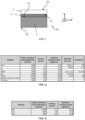
- the hybrid structure 10 comprises a useful layer 1 of piezoelectric material, having a first face 1a and a second face 1b, as illustrated in the figure 1 .
- the useful layer 1 is so named because it will be used for the subsequent development of surface acoustic wave devices.
- the useful layer 1 of the hybrid structure 10 may be composed of a material chosen from the group: lithium tantalate LiTaO3 (LTO in table 1b), lithium niobate LiNbO 3 (LNO in table 1b ), aluminum nitride AlN (Table 1b), zinc oxide (ZnO).
- the hybrid structure 10 also includes an intermediate layer 3 arranged under the useful layer 1 (along the z axis represented on the figure 1 ).
- the middle layer is a sintered composite layer 3, formed from powders of at least two different materials.
- sintered layer is meant a layer resulting from the consolidation of a mixture of powders: this consolidation is obtained by supplying thermal and possibly mechanical energy, but without melting at least one of the powdery materials of the mixture.
- the sintered nature of the composite layer can therefore be detected by structural analysis of said layer (for example by scanning electron microscopy).
- the particles or grains of the material powders appear welded together and the density of the composite layer depends on the level of compaction of the mixture during the contribution of energy for the consolidation.
- the particles forming the powder of each of the materials of the sintered composite layer 3 have dimensions following a typically Gaussian distribution. In the rest of the description, the mean size of the particles will be assimilated to the mean equivalent diameter of the particles of a given material.
- the average particle size can typically vary between a few tens of nanometers and a few microns.
- the sintered composite layer 3 can in particular be formed from at least a first and a second material, chosen from among silicon oxide, silicon nitride, silicon, silicon carbide, alumina, germanium , sapphire, zirconium, some properties of which are shown in Table 1.
- the sintered composite layer 3 may optionally comprise three or more different materials.
- the sintered composite layer 3 has, according to the embodiments, a thickness of between a few hundred nanometers and several microns.
- the hybrid structure 10 comprises a support substrate 2 having a coefficient of thermal expansion lower than that of the useful layer 1, placed under the composite layer 3 (along the axis z represented on the figure 1 ), making it possible to limit the expansion/contraction of the useful layer 1 in temperature (and thus to improve the thermal frequency coefficient of the devices which will be produced on said useful layer 1).
- the support substrate 2 may in particular be composed of a material chosen from the group: silicon, III-V semiconductors, silicon carbide, glass, sapphire.
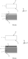
- the hybrid structure 10 preferably comprises additional layers 4 arranged on the first face 1a of the useful layer 1 and/or on the first face 2a of the support substrate 2, and potentially on the second face 2b of the support substrate 2 and on the edges of said substrate 2 ( figure 2b ).
- these additional layers 4 have in particular a function of protecting the support substrate 2 and/or the useful layer 1, against the diffusion of impurities contained in the sintered composite layer 3 or present during the production of said layer 3.
- the hybrid structure 10 according to the invention is suitable for the manufacture of surface acoustic wave (SAW) devices, comprising in particular metal electrodes 20 on the useful layer 1, between which an acoustic signal propagates (schematized by the white arrow on there picture 3 ), in the plane (x,y), close to the surface of the second face 1b of the useful layer 1.
- SAW surface acoustic wave
- the sintered composite layer 3 is configured to maximize the diffusion of an incident acoustic wave, resulting from the acoustic signal and which would propagate in the volume of the useful layer 1 , up to composite layer 3.
- the first material in the sintered composite layer 3, formed from powders of at least a first and a second material, has an acoustic impedance similar to that of the useful layer 1.
- similar is meant having a difference maximum of +/-20% around the value of acoustic impedance of the useful layer 1, and preferably a deviation of less than +/-15%, or even +/-10%.
- the first material can be alumina, whose acoustic impedance (40.6 ⁇ 10 6 Pa.s/m) is substantially the same as that of lithium tantalate (44.8 ⁇ 10 6 Pa.s/m).
- the ratio between the acoustic impedance of the useful layer 1 and the acoustic impedance of the second material of the sintered composite layer 3 is chosen to be greater than or equal to 2, so as to guarantee a reflection coefficient of more than 10 %.
- the first material is lithium tantalate (44.8 ⁇ 10 6 Pa.s/m)
- the second material could be SiO2, whose acoustic impedance is 13.2 ⁇ 10 6 Pa.s/ m, making it possible to obtain a reflection coefficient of the order of 30% at the interface between the particles of the composite layer 3, and producing reflections in multiple directions (diffusion).
- the size of the particles of the powders of the first and of the second material is greater than or equal to a quarter of the wavelength of the incident acoustic wave. This characteristic ensures that the incident acoustic wave can be influenced by the particles. For example, for an incident acoustic wave with a wavelength around 6 microns (i.e. a frequency of around 1 GHz), the average size particles will be chosen around 2 microns.
- the sintered composite layer 3 then has a thickness greater than 5 microns, or even greater than 10 microns.
- the additional layer 4 must have an acoustic impedance close to that of the useful layer 1, to limit the parasitic reflections between these two layers.
- a useful layer 1 in LiTaO3 it is possible for example to use alumina whose acoustic impedance (40.6 ⁇ 10 6 Pa.s/m) is close to that of LiTaO3, which leads to a reflection of less than 0.5 %.
- the sintered composite layer 3 according to the first embodiment makes it possible to diffuse the incident wave in a multitude of directions, and thus greatly limits the component reflected towards the electrodes 20 of the surface acoustic wave device.
- the sintered composite layer 3 is configured to maximize the transmission of an incident acoustic wave, coming from the acoustic signal and which would propagate in the volume of the useful layer 1 , up to composite layer 3.
- the first material and the second material are chosen so as to form an acoustic impedance matching layer between the useful layer 1 and the support substrate 2.
- Forming an acoustic impedance matching layer implies that the average acoustic impedance of the composite layer 3 is substantially equal to the square root of the product of the acoustic impedances of the useful layer 1 and of the support substrate 2: Z layer composite ⁇ Z layer useful ⁇ Z substrate
- volume fractions V 1 and V 2 are defined by the proportion of each of the materials in the composite layer 3.
- the first material may be Al 2 O 3 and the second material SiO 2 , present in the composite layer in proportions of 65% and 35% respectively.
- the impedance of the composite layer 3 could thus be of the order of 30 ⁇ 10 6 Pa.s/m.
- the average size of the particles of the powders of the first and of the second material is less than a quarter of the wavelength of the incident acoustic wave. This characteristic ensures that the incident acoustic wave sees the composite layer as an almost homogeneous medium.
- the average size of the particles could be chosen around 0.5 microns.
- Layer sintered composite 3 may have a thickness of a few microns.
- the additional layer 4 must have an acoustic impedance close to that of the useful layer 1, to limit the parasitic reflections between these two layers.
- a useful layer 1 in LiTaO3 it is possible for example to use alumina whose acoustic impedance (40.6 ⁇ 10 6 Pa.s/m) is close to that of LiTaO3, which leads to a reflection of less than 0.5 %.
- an additional layer 4 is present between the composite layer 3 and the support substrate 2, this additional layer 4 must have an acoustic impedance close to that of the support substrate 2, to limit parasitic reflections at the additional layer/support substrate interface.
- silicon nitride may for example be used whose acoustic impedance ( ⁇ 22 ⁇ 10 6 Pa.s/m) is close to that of Si, which leads to a reflection of less than 0.5 %.
- the sintered composite layer 3 according to the second embodiment makes it possible to favor the transmission (by acoustic impedance matching) from the useful layer 1 to the substrate 2, of the incident acoustic wave usually reflecting at the interfaces of a hybrid structure : it therefore makes it possible to reduce the parasitic reflections negatively impacting the frequency characteristics of the SAW device produced on the hybrid structure 10.
- the sintered composite layer 3 has good dielectric properties (resistivity greater than 1 E 7 ohms.cm) and a low equivalent permittivity (typically less than 11 F/m, permittivity of silicon), so as to provide electrical insulation equivalent to several microns of silicon oxide.
- a sintered composite layer 3 can in particular improve the linearity of the surface acoustic wave device in the radio frequency domain.
- the sintered composite layer 3 has properties for trapping mobile electrical charges. This characteristic makes it possible to trap and therefore to neutralize the electric charges liable to appear in the upper part of the support substrate 2 due to the presence of fixed charges in one of the upper layers (additional layer 4 or useful layer 1). To present this trapping characteristic, one of the materials making up the particles of the composite layer 3 may be silicon.
- the invention also relates to a method of manufacturing a hybrid structure 10 for a surface acoustic wave device.
- the method comprises a first step (denoted i)) of supplying a useful layer 1 of piezoelectric material.
- the useful layer 1 is in the form of a donor substrate 1' of piezoelectric material, of standard thickness and diameter for the microelectronics industry ( figure 4a ).
- the first step also includes the supply of a support substrate 2 having a coefficient of thermal expansion lower than that of the donor substrate 1' (ie also that of the useful layer 1).
- the manufacturing method according to the invention comprises a second step (denoted ii)) comprising the deposition of a layer 3' formed of a mixture of powders of at least a first material and a second material different from the first, on a first face 1a of the useful layer 1 (or of the donor substrate 1') and/or on a first face 2a of the support substrate 2.
- the deposition of the layer 3′ of powder mixture is carried out on the first face 2a of the support substrate 2.
- the layer 3′ could be deposited on the first face 1a of the useful layer 1; it could also be deposited on each of the first faces 1a, 2a respectively of the useful layer 1 and of the support substrate 2.
- the first face 2a of the support substrate 2 comprises a protective layer 4a prepared prior to the deposition of the layer 3' of mixture of powders.
- the protective layer 4a may even completely encapsulate the support substrate 2, that is to say cover its rear face 2b and its edge.
- a protective layer will be deposited at least on the first face 1a of said useful layer 1 (or of the donor substrate 1').
- the protective layer 4a is formed by at least one material chosen from among silicon nitride, silicon oxynitride, silicon oxide, alumina. It can be produced by various known techniques of chemical deposition. It makes it possible to avoid or at least to limit the diffusion of impurities contained in the layer 3′, in the support substrate 2 (or the useful layer 1)
- the mixture of powders is in the form of a viscous paste.
- Such a paste is usually obtained by adding a liquid compound, of the solvent type (in particular alcohol, for example ethanol), to the dry mixture of powders.
- a liquid compound of the solvent type (in particular alcohol, for example ethanol)
- the powders used contain particles whose average size is between a few tens of nanometers and a few microns.
- the mixture of powders can be integrated into a matrix of the silicon-based polymer type (PDC for polymer-derived ceramics), capable of being transformed into ceramic at high temperature.
- PDC silicon-based polymer type
- the sintered composite layer 3 which will be obtained subsequently will comprise the first and the second material coming from the mixture of powders, but also silicon coming from the transformation into ceramic of the matrix.
- the deposition of the layer 3′ formed by said mixture in step ii) is preferably carried out by centrifugal coating (“spin coating” or “dip coating” according to English terminology) or screen printing through a mask.
- the viscosity of the paste is adjusted by the powder/liquid compound (solvent and/or polymer) ratio. It is chosen to allow a uniform deposition of the layer 3′, at thicknesses that can range from a few hundred nanometers to several microns.
- the deposition of the 3' layer is followed by a heat treatment at low temperatures (for example between 150°C and 400°C) making it possible to evacuate the solvent(s) from the 3' layer and to avoid any degassing later in the process, in particular after the assembly step (described later).
- low temperatures for example between 150°C and 400°C
- the mixture of powders is in a dry pulverulent form and is deposited in a layer 3' on the first face 2a of the support substrate 2 (or alternatively on the face 1a of the donor substrate 1').
- This layer 3' can be shaped by compression molding or hot isostatic compression. In both cases, a compressive stress is applied to layer 3' to make the particles of the powders of the mixture integral with each other and with the first face 2a. Specific tools are required to maintain the powder mixture on the substrate and apply a uniform compressive stress over the entire surface of said substrate.
- the manufacturing method according to the invention comprises a third step (denoted iii)) comprising the sintering of the layer 3′ formed from the mixture of powders, to obtain a sintered composite layer 3 integral with the first face 2a of the support substrate 2 ( figure 4c ).
- Sintering usually takes place at high temperatures, typically above 1000° C., for a period that can range from a few hours to about 24 hours.
- the sintering temperature nevertheless remains lower than the melting temperature of at least one of the powders contained in layer 3'. Under the effect of heat, the particles of the powders weld together, which forms the cohesion of the resulting composite layer 3.
- the composite layer 3 is also joined with the first face 2a of the support substrate 2.
- the sintering can also be carried out under mechanical stress, which makes it possible to further compact the composite layer 3.
- the sintered composite layer 3 is thus composed of at least particles of the first and of the second material. Between the particles, depending on the level of compaction, there may be more or less empty interstices (or containing the ceramic resulting from a PDC matrix). Depending on the size distribution of the particles, the volume fraction of these interstices may reach 50%, and more preferably be kept below 25%, or even below 15%, in particular to ensure good mechanical strength of the composite layer 3. for simplicity, this volume fraction of interstices has not been taken into account in the embodiments of the hybrid structure 10 described above; it could be considered as a third material, in addition to the first and second materials composing the particles.
- the thickness of the layer 3′ deposited in step ii) is chosen so as to obtain a desired thickness of sintered composite layer 3. Indeed, depending on the type of layer 3′ deposited (in the form of a paste with solvent and/or or polymer or in dry form), the reduction in thickness during the sintering step will be more or less significant. A reduction in volume of the 3′ layer of the order of 10 to 30% can take place.
- the manufacturing method according to the invention comprises a fourth step (denoted iv)) comprising the assembly of the useful layer 1 (or of the donor substrate 1') and of the support substrate 2, so that the sintered composite layer 3 is placed between the useful layer 1 and the support substrate 2 ( 4d figure ).
- an adhesive layer 4b is deposited on the composite layer 3, prior to step iv) of assembly.
- a layer of silicon oxide can be deposited on the free surface of the composite layer 3.
- This bonding layer 4b provides, on the one hand, an encapsulation of the sintered composite layer 3, avoiding or at least less limiting the risks of contamination between the different layers of the hybrid structure 10; on the other hand, the bonding layer 4b can be advantageous to allow a conventional surface preparation that is not specific to the composition of the sintered composite layer 3.
- the assembly step is carried out by direct bonding, by molecular adhesion of the two surfaces brought into contact: that is to say of the first face 1a of the useful layer 1 (or of the donor substrate 1') and of the free face of the composite layer 3 on the example of the figure 4c .
- molecular adhesion well known in the state of the art, will not be described in more detail here.
- the assembly may be carried out by adding a layer of adhesive material, or by any other bonding technique suitable for the intended application.
- the manufacturing method according to the invention may further comprise a fifth step (denoted v)) comprising the thinning of the donor substrate 1′ down to the desired thickness of the useful layer 1 for manufacturing the acoustic wave device ( figure 4e ).
- This step may, for example, comprise mechanical lapping (“grinding”) followed by dry or mechanical-chemical polishing, making it possible to ensure a good surface condition for the useful layer 1.
- Different cleaning sequences may be applied during or after the thinning step to ensure the quality and cleanliness of the final hybrid structure 10.
- the thinning of the donor substrate 1' to obtain the useful layer 1 can be carried out by any other technique known, in particular the Smart Cut ® process or other techniques for producing thin layers.
Landscapes
- Physics & Mathematics (AREA)
- Acoustics & Sound (AREA)
- Engineering & Computer Science (AREA)
- Manufacturing & Machinery (AREA)
- Chemical & Material Sciences (AREA)
- Materials Engineering (AREA)
- Inorganic Chemistry (AREA)
- Surface Acoustic Wave Elements And Circuit Networks Thereof (AREA)
Claims (12)
- Hybridstruktur (10) für eine Vorrichtung mit akustischen Oberflächenwellen, umfassend eine Nutzschicht (1) aus piezoelektrischem Material, die mit einem Trägersubstrat (2) zusammengefügt ist, das einen kleineren Wärmeausdehnungskoeffizienten als der der Nutzschicht (1) aufweist, und eine Zwischenschicht (3), die zwischen der Nutzschicht (1) und dem Trägersubstrat (2) gelegen ist, wobei die Zwischenschicht (3) eine Sinterverbundschicht (3) ist, die aus Pulvern mindestens eines ersten Materials und eines zweiten Materials, das sich von dem ersten unterscheidet, gebildet wird, wobei die Hybridstruktur (10)
dadurch gekennzeichnet ist, dass:- das erste Material und das zweite Material so ausgewählt sind, dass sie eine Schicht zum Anpassen einer akustischen Impedanz zwischen der Nutzschicht (1) und dem Trägersubstrat (2) bilden, und- die durchschnittliche Größe von Pulverpartikeln des ersten und des zweiten Materials weniger als ein Viertel der Wellenlänge eines akustischen Signals beträgt, das dafür bestimmt ist, sich an einer Oberfläche der Vorrichtung mit akustischen Oberflächenwellen auszubreiten. - Hybridstruktur (10) für eine Vorrichtung mit akustischen Oberflächenwellen nach dem vorstehenden Anspruch, wobei das Trägersubstrat (2) ein Material umfasst, das ausgewählt ist aus Silizium, Glas, Siliziumdioxid, Saphir, Aluminiumoxid und Aluminiumnitrid.
- Hybridstruktur (10) für eine Vorrichtung mit akustischen Oberflächenwellen nach einem der vorstehenden Ansprüche, wobei die Nutzschicht (1) ein piezoelektrisches Material umfasst, das ausgewählt ist aus Lithiumtantalat (LiTaO3), Lithiumniobat (LiNbO3), Quarz, Zinkoxid (ZnO).
- Hybridstruktur (10) für eine Vorrichtung mit akustischen Oberflächenwellen nach einem der vorstehenden Ansprüche, wobei das erste und das zweite Material ausgewählt sind aus Siliziumoxid, Siliziumnitrid, Silizium, Siliziumkarbid, Aluminiumoxid, Germanium, Saphir, Zirkonium.
- Verfahren zum Herstellen einer Hybridstruktur (10) für eine Vorrichtung mit akustischen Oberflächenwellen, dadurch gekennzeichnet, dass es die folgenden Schritte umfasst:i) das Bereitstellen einer Nutzschicht (1) aus piezoelektrischem Material und eines Trägersubstrats (2), das einen kleineren Wärmeausdehnungskoeffizienten als der der Nutzschicht (1) aufweist;ii) das Aufbringen einer Schicht (3'), die aus einer Mischung von Pulvern von mindestens einem ersten Material und einem zweiten Material, das sich von dem ersten unterscheidet, gebildet wird, auf eine erste Seite (1a) der Nutzschicht (1) und/oder auf eine erste Seite (2a) des Trägersubstrats (2); wobei das erste Material und das zweite Material so ausgewählt sind, dass sie eine Schicht zum Anpassen der akustischen Impedanz zwischen der Nutzschicht (1) und dem Trägersubstrat (2) bilden, und wobei die durchschnittliche Größe der Pulverpartikel des ersten und des zweiten Materials kleiner als ein Viertel der Wellenlänge eines akustischen Signals ist, das dafür bestimmt ist, sich an der Oberfläche der Vorrichtung mit akustischen Oberflächenwellen auszubreiten;iii) das Sintern der Schicht (3'), die aus der Pulvermischung gebildet wird, um eine Sinterverbundschicht (3) zu erhalten, die fest mit der ersten Seite (1a) der Nutzschicht (1) und/oder der ersten Seite (2a) des Trägersubstrats (2) verbunden ist;iv) das Zusammenfügen der Nutzschicht (1) und des Trägersubstrats (2), so dass die Verbundschicht (3) zwischen der Nutzschicht (1) und dem Trägersubstrat (2) angeordnet ist.
- Verfahren zum Herstellen einer Hybridstruktur (10) für eine Vorrichtung mit akustischen Oberflächenwellen nach dem vorstehenden Anspruch, wobei die erste Seite (1a) der Nutzschicht (1) und/oder die erste Seite (2a) des Trägersubstrats (2) eine Schutzschicht (4, 4a) aufweist, vor dem Aufbringen der Schicht (3'), die aus der Pulvermischung gebildet wird, von Schritt ii).
- Verfahren zum Herstellen einer Hybridstruktur (10) für eine Vorrichtung mit akustischen Oberflächenwellen nach dem vorstehenden Anspruch, wobei die Schutzschicht (4, 4a) aus mindestens einem Material gebildet wird, das ausgewählt ist aus Siliziumnitrid, einem Siliziumoxynitrid, einem Siliziumoxid und Aluminiumoxid.
- Verfahren zum Herstellen einer Hybridstruktur (10) für eine Vorrichtung mit akustischen Oberflächenwellen nach einem der drei vorstehenden Ansprüche, wobei die Pulvermischung in Form einer viskosen Paste vorhanden ist und das Aufbringen der Schicht (3'), die durch die Mischung gebildet wird, in Schritt ii) durch Zentrifugalbeschichtung erfolgt.
- Verfahren zum Herstellen einer Hybridstruktur (10) für eine Vorrichtung mit akustischen Oberflächenwellen nach dem vorstehenden Anspruch, wobei auf das Aufbringen der durch die Pulvermischung gebildeten Schicht (3') eine Wärmebehandlung bei niedriger Temperatur folgt, um mindestens eine flüssige Komponente aus der viskosen Paste zu entziehen.
- Verfahren zum Herstellen einer Hybridstruktur (10) für eine Vorrichtung mit akustischen Oberflächenwellen nach einem der fünf vorstehenden Ansprüche, wobei vor dem Schritt iv) des Zusammenfügens eine Klebeschicht (4b) auf die Verbundschicht (3) aufgebracht wird.
- Verfahren zum Herstellen einer Hybridstruktur (10) für eine Vorrichtung mit akustischen Oberflächenwellen nach einem der sechs vorstehenden Ansprüche, wobei die in Schritt i) bereitgestellte Nutzschicht (1) ein Donorsubstrat (1') aus piezoelektrischem Material ist.
- Verfahren zum Herstellen einer Hybridstruktur (10) für eine Vorrichtung mit akustischen Oberflächenwellen nach dem vorstehenden Anspruch, umfassend einen Schritt v) eines Verdünnens des Donorsubstrats (1') bis zu der gewünschten Dicke der Nutzschicht (1) für die Herstellung der Vorrichtung mit akustischen Wellen.
Applications Claiming Priority (3)
| Application Number | Priority Date | Filing Date | Title |
|---|---|---|---|
| FR1852796A FR3079666B1 (fr) | 2018-03-30 | 2018-03-30 | Structure hybride pour dispositif a ondes acoustiques de surface et procede de fabrication associe |
| EP19715974.2A EP3776677B1 (de) | 2018-03-30 | 2019-03-13 | Hybridstruktur für oberflächenschallwellenvorrichtung und zugehöriges herstellungsverfahren |
| PCT/FR2019/050540 WO2019186011A1 (fr) | 2018-03-30 | 2019-03-13 | Structure hybride pour dispositif a ondes acoustiques de surface et procede de fabrication associe |
Related Parent Applications (2)
| Application Number | Title | Priority Date | Filing Date |
|---|---|---|---|
| EP19715974.2A Division-Into EP3776677B1 (de) | 2018-03-30 | 2019-03-13 | Hybridstruktur für oberflächenschallwellenvorrichtung und zugehöriges herstellungsverfahren |
| EP19715974.2A Division EP3776677B1 (de) | 2018-03-30 | 2019-03-13 | Hybridstruktur für oberflächenschallwellenvorrichtung und zugehöriges herstellungsverfahren |
Publications (2)
| Publication Number | Publication Date |
|---|---|
| EP4012790A1 EP4012790A1 (de) | 2022-06-15 |
| EP4012790B1 true EP4012790B1 (de) | 2023-07-19 |
Family
ID=63407293
Family Applications (2)
| Application Number | Title | Priority Date | Filing Date |
|---|---|---|---|
| EP19715974.2A Active EP3776677B1 (de) | 2018-03-30 | 2019-03-13 | Hybridstruktur für oberflächenschallwellenvorrichtung und zugehöriges herstellungsverfahren |
| EP21217508.7A Active EP4012790B1 (de) | 2018-03-30 | 2019-03-13 | Hybridstruktur für vorrichtung mit oberflächenschallwellen und entsprechendes herstellungsverfahren |
Family Applications Before (1)
| Application Number | Title | Priority Date | Filing Date |
|---|---|---|---|
| EP19715974.2A Active EP3776677B1 (de) | 2018-03-30 | 2019-03-13 | Hybridstruktur für oberflächenschallwellenvorrichtung und zugehöriges herstellungsverfahren |
Country Status (9)
| Country | Link |
|---|---|
| US (1) | US11974505B2 (de) |
| EP (2) | EP3776677B1 (de) |
| JP (1) | JP7480930B2 (de) |
| KR (1) | KR102673839B1 (de) |
| CN (2) | CN120379511A (de) |
| FR (1) | FR3079666B1 (de) |
| SG (1) | SG11202009517QA (de) |
| TW (1) | TWI780312B (de) |
| WO (1) | WO2019186011A1 (de) |
Families Citing this family (9)
| Publication number | Priority date | Publication date | Assignee | Title |
|---|---|---|---|---|
| EP3852387A1 (de) * | 2020-01-16 | 2021-07-21 | Nederlandse Organisatie voor toegepast- natuurwetenschappelijk Onderzoek TNO | Schallerfassungsvorrichtung |
| CN111755588B (zh) * | 2020-06-17 | 2024-07-09 | 济南晶正电子科技有限公司 | 一种复合单晶压电基板及其制备方法 |
| CN113541626B (zh) * | 2020-04-21 | 2025-07-22 | 济南晶正电子科技有限公司 | 一种复合单晶压电基板及制备方法 |
| CN113540339B (zh) * | 2020-04-21 | 2024-07-12 | 济南晶正电子科技有限公司 | 一种制备压电复合薄膜的方法及压电复合薄膜 |
| WO2021213410A1 (zh) * | 2020-04-21 | 2021-10-28 | 济南晶正电子科技有限公司 | 一种复合基板及其制备方法 |
| WO2022065138A1 (ja) * | 2020-09-25 | 2022-03-31 | 株式会社村田製作所 | 弾性波デバイスおよび弾性波モジュール |
| CN112787618B (zh) * | 2020-12-25 | 2022-10-14 | 济南晶正电子科技有限公司 | 一种压电衬底、制备方法及电子元器件 |
| CN112688658B (zh) * | 2020-12-25 | 2021-11-26 | 济南晶正电子科技有限公司 | 一种压电衬底、制备方法及电子元器件 |
| CN118573145B (zh) * | 2024-08-01 | 2024-12-20 | 泉州市三安集成电路有限公司 | 支撑基板及其制备方法、复合基板、电子器件和模块 |
Family Cites Families (14)
| Publication number | Priority date | Publication date | Assignee | Title |
|---|---|---|---|---|
| GB9505038D0 (en) * | 1994-10-01 | 1995-05-03 | Imas Uk Ltd | A filter, apparatus including the filter and a method of use of the apparatus |
| JP2004006645A (ja) | 2002-04-19 | 2004-01-08 | Seiko Epson Corp | 圧電体素子の製造方法、圧電体素子並びに液滴吐出式記録ヘッド |
| GB2469869A (en) * | 2009-05-01 | 2010-11-03 | Univ Bolton | Continuous ZnO films |
| JP2010018514A (ja) | 2009-07-13 | 2010-01-28 | Seiko Epson Corp | 圧電材料の製造方法、圧電素子および圧電発電機 |
| FR2951336B1 (fr) * | 2009-10-09 | 2017-02-10 | Commissariat Energie Atomique | Dispositif a ondes acoustiques comprenant un filtre a ondes de surface et un filtre a ondes de volume et procede de fabrication |
| CN106209007B (zh) | 2010-12-24 | 2019-07-05 | 株式会社村田制作所 | 弹性波装置 |
| JP5556966B2 (ja) * | 2011-08-08 | 2014-07-23 | パナソニック株式会社 | 圧電体素子 |
| WO2013026125A1 (en) | 2011-08-24 | 2013-02-28 | National Research Council Of Canada | Porosity control in piezoelectric films |
| CN103085372B (zh) * | 2011-10-31 | 2015-10-07 | 深圳光启高等理工研究院 | 一种超材料介质基板及其加工方法 |
| CN105164919B (zh) | 2013-03-21 | 2017-04-26 | 日本碍子株式会社 | 弹性波元件用复合基板及弹性波元件 |
| WO2016157854A1 (en) | 2015-04-03 | 2016-10-06 | Canon Kabushiki Kaisha | Piezoelectric material, method of producing piezoelectric material, piezoelectric element, and electronic apparatus |
| FR3047355B1 (fr) * | 2016-02-01 | 2019-04-19 | Soitec | Structure hybride pour dispositif a ondes acoustiques de surface |
| WO2017163722A1 (ja) | 2016-03-25 | 2017-09-28 | 日本碍子株式会社 | 接合方法 |
| KR20190134827A (ko) | 2016-03-25 | 2019-12-04 | 엔지케이 인슐레이터 엘티디 | 접합체 및 탄성파 소자 |
-
2018
- 2018-03-30 FR FR1852796A patent/FR3079666B1/fr active Active
-
2019
- 2019-03-13 US US17/044,132 patent/US11974505B2/en active Active
- 2019-03-13 CN CN202510462420.XA patent/CN120379511A/zh active Pending
- 2019-03-13 EP EP19715974.2A patent/EP3776677B1/de active Active
- 2019-03-13 CN CN201980018383.6A patent/CN111837247B/zh active Active
- 2019-03-13 JP JP2020543227A patent/JP7480930B2/ja active Active
- 2019-03-13 EP EP21217508.7A patent/EP4012790B1/de active Active
- 2019-03-13 KR KR1020207030979A patent/KR102673839B1/ko active Active
- 2019-03-13 SG SG11202009517QA patent/SG11202009517QA/en unknown
- 2019-03-13 WO PCT/FR2019/050540 patent/WO2019186011A1/fr not_active Ceased
- 2019-03-14 TW TW108108632A patent/TWI780312B/zh active
Also Published As
| Publication number | Publication date |
|---|---|
| JP7480930B2 (ja) | 2024-05-10 |
| US11974505B2 (en) | 2024-04-30 |
| FR3079666B1 (fr) | 2020-04-03 |
| TW201946299A (zh) | 2019-12-01 |
| CN111837247B (zh) | 2025-05-06 |
| SG11202009517QA (en) | 2020-10-29 |
| CN111837247A (zh) | 2020-10-27 |
| KR20200135521A (ko) | 2020-12-02 |
| JP2021517384A (ja) | 2021-07-15 |
| FR3079666A1 (fr) | 2019-10-04 |
| TWI780312B (zh) | 2022-10-11 |
| US20210057635A1 (en) | 2021-02-25 |
| CN120379511A (zh) | 2025-07-25 |
| EP3776677A1 (de) | 2021-02-17 |
| EP3776677B1 (de) | 2022-02-16 |
| EP4012790A1 (de) | 2022-06-15 |
| KR102673839B1 (ko) | 2024-06-10 |
| WO2019186011A1 (fr) | 2019-10-03 |
Similar Documents
| Publication | Publication Date | Title |
|---|---|---|
| EP4012790B1 (de) | Hybridstruktur für vorrichtung mit oberflächenschallwellen und entsprechendes herstellungsverfahren | |
| EP3694008B1 (de) | Hybridstruktur für vorrichtung mit oberflächenschallwellen | |
| EP2464006B1 (de) | Herstellungsverfahren eines Schallwellenresonators, der eine aufgehängte Membran umfasst | |
| EP3411910B1 (de) | Hybridstruktur für eine oberflächenschallwellenvorrichtung | |
| WO2017068268A1 (fr) | Dispositif à ondes acoustiques de surface et procédé de fabrication associé | |
| EP3465784B1 (de) | Hybridstruktur für eine oberflächenschallwellenvorrichtung | |
| EP2486655A1 (de) | Schallwellenvorrichtug mit einem oberflächenwellenfilter und einem volumenwellenfilter sowie herstellungsverfahren dafür | |
| EP3394908B1 (de) | Substrat für eine temperaturkompensierte oberflächenschallwellenvorrichtung oder volumenschallwellenvorrichtung | |
| EP3776640B1 (de) | Substrat für radiofrequenzanwendungen und zugehöriges herstellungsverfahren | |
| EP4391374A1 (de) | Verfahren zur herstellung eines akustischen volumenwellenfilters | |
| WO2024009046A1 (fr) | Procédé de fabrication d'une structure semi-conductrice ou piézoélectrique | |
| FR3108788A1 (fr) | Procédé de fabrication d’une structure piézoélectrique pour dispositif radiofréquence et pouvant servir pour le transfert d’une couche piézoélectrique, et procédé de transfert d’une telle couche piézoélectrique |
Legal Events
| Date | Code | Title | Description |
|---|---|---|---|
| PUAI | Public reference made under article 153(3) epc to a published international application that has entered the european phase |
Free format text: ORIGINAL CODE: 0009012 |
|
| STAA | Information on the status of an ep patent application or granted ep patent |
Free format text: STATUS: REQUEST FOR EXAMINATION WAS MADE |
|
| 17P | Request for examination filed |
Effective date: 20211223 |
|
| AC | Divisional application: reference to earlier application |
Ref document number: 3776677 Country of ref document: EP Kind code of ref document: P |
|
| AK | Designated contracting states |
Kind code of ref document: A1 Designated state(s): AL AT BE BG CH CY CZ DE DK EE ES FI FR GB GR HR HU IE IS IT LI LT LU LV MC MK MT NL NO PL PT RO RS SE SI SK SM TR |
|
| REG | Reference to a national code |
Ref country code: DE Ref legal event code: R079 Free format text: PREVIOUS MAIN CLASS: H01L0041430000 Ipc: H10N0030097000 Ref country code: DE Ref legal event code: R079 Ref document number: 602019033340 Country of ref document: DE Free format text: PREVIOUS MAIN CLASS: H01L0041430000 Ipc: H10N0030097000 |
|
| GRAP | Despatch of communication of intention to grant a patent |
Free format text: ORIGINAL CODE: EPIDOSNIGR1 |
|
| STAA | Information on the status of an ep patent application or granted ep patent |
Free format text: STATUS: GRANT OF PATENT IS INTENDED |
|
| RIC1 | Information provided on ipc code assigned before grant |
Ipc: H10N 30/079 20230101ALI20230110BHEP Ipc: H10N 30/00 20230101ALI20230110BHEP Ipc: H10N 30/097 20230101AFI20230110BHEP |
|
| INTG | Intention to grant announced |
Effective date: 20230206 |
|
| RIN1 | Information on inventor provided before grant (corrected) |
Inventor name: VEYTIZOU, CHRISTELLE Inventor name: ALLIBERT, FREDERIC |
|
| GRAS | Grant fee paid |
Free format text: ORIGINAL CODE: EPIDOSNIGR3 |
|
| GRAA | (expected) grant |
Free format text: ORIGINAL CODE: 0009210 |
|
| STAA | Information on the status of an ep patent application or granted ep patent |
Free format text: STATUS: THE PATENT HAS BEEN GRANTED |
|
| AC | Divisional application: reference to earlier application |
Ref document number: 3776677 Country of ref document: EP Kind code of ref document: P |
|
| AK | Designated contracting states |
Kind code of ref document: B1 Designated state(s): AL AT BE BG CH CY CZ DE DK EE ES FI FR GB GR HR HU IE IS IT LI LT LU LV MC MK MT NL NO PL PT RO RS SE SI SK SM TR |
|
| REG | Reference to a national code |
Ref country code: GB Ref legal event code: FG4D Free format text: NOT ENGLISH |
|
| REG | Reference to a national code |
Ref country code: CH Ref legal event code: EP |
|
| REG | Reference to a national code |
Ref country code: DE Ref legal event code: R096 Ref document number: 602019033340 Country of ref document: DE |
|
| REG | Reference to a national code |
Ref country code: IE Ref legal event code: FG4D Free format text: LANGUAGE OF EP DOCUMENT: FRENCH |
|
| REG | Reference to a national code |
Ref country code: LT Ref legal event code: MG9D |
|
| REG | Reference to a national code |
Ref country code: NL Ref legal event code: MP Effective date: 20230719 |
|
| REG | Reference to a national code |
Ref country code: AT Ref legal event code: MK05 Ref document number: 1590810 Country of ref document: AT Kind code of ref document: T Effective date: 20230719 |
|
| PG25 | Lapsed in a contracting state [announced via postgrant information from national office to epo] |
Ref country code: NL Free format text: LAPSE BECAUSE OF FAILURE TO SUBMIT A TRANSLATION OF THE DESCRIPTION OR TO PAY THE FEE WITHIN THE PRESCRIBED TIME-LIMIT Effective date: 20230719 |
|
| PG25 | Lapsed in a contracting state [announced via postgrant information from national office to epo] |
Ref country code: GR Free format text: LAPSE BECAUSE OF FAILURE TO SUBMIT A TRANSLATION OF THE DESCRIPTION OR TO PAY THE FEE WITHIN THE PRESCRIBED TIME-LIMIT Effective date: 20231020 |
|
| PG25 | Lapsed in a contracting state [announced via postgrant information from national office to epo] |
Ref country code: IS Free format text: LAPSE BECAUSE OF FAILURE TO SUBMIT A TRANSLATION OF THE DESCRIPTION OR TO PAY THE FEE WITHIN THE PRESCRIBED TIME-LIMIT Effective date: 20231119 |
|
| PG25 | Lapsed in a contracting state [announced via postgrant information from national office to epo] |
Ref country code: SE Free format text: LAPSE BECAUSE OF FAILURE TO SUBMIT A TRANSLATION OF THE DESCRIPTION OR TO PAY THE FEE WITHIN THE PRESCRIBED TIME-LIMIT Effective date: 20230719 Ref country code: RS Free format text: LAPSE BECAUSE OF FAILURE TO SUBMIT A TRANSLATION OF THE DESCRIPTION OR TO PAY THE FEE WITHIN THE PRESCRIBED TIME-LIMIT Effective date: 20230719 Ref country code: PT Free format text: LAPSE BECAUSE OF FAILURE TO SUBMIT A TRANSLATION OF THE DESCRIPTION OR TO PAY THE FEE WITHIN THE PRESCRIBED TIME-LIMIT Effective date: 20231120 Ref country code: NO Free format text: LAPSE BECAUSE OF FAILURE TO SUBMIT A TRANSLATION OF THE DESCRIPTION OR TO PAY THE FEE WITHIN THE PRESCRIBED TIME-LIMIT Effective date: 20231019 Ref country code: LV Free format text: LAPSE BECAUSE OF FAILURE TO SUBMIT A TRANSLATION OF THE DESCRIPTION OR TO PAY THE FEE WITHIN THE PRESCRIBED TIME-LIMIT Effective date: 20230719 Ref country code: LT Free format text: LAPSE BECAUSE OF FAILURE TO SUBMIT A TRANSLATION OF THE DESCRIPTION OR TO PAY THE FEE WITHIN THE PRESCRIBED TIME-LIMIT Effective date: 20230719 Ref country code: IS Free format text: LAPSE BECAUSE OF FAILURE TO SUBMIT A TRANSLATION OF THE DESCRIPTION OR TO PAY THE FEE WITHIN THE PRESCRIBED TIME-LIMIT Effective date: 20231119 Ref country code: HR Free format text: LAPSE BECAUSE OF FAILURE TO SUBMIT A TRANSLATION OF THE DESCRIPTION OR TO PAY THE FEE WITHIN THE PRESCRIBED TIME-LIMIT Effective date: 20230719 Ref country code: GR Free format text: LAPSE BECAUSE OF FAILURE TO SUBMIT A TRANSLATION OF THE DESCRIPTION OR TO PAY THE FEE WITHIN THE PRESCRIBED TIME-LIMIT Effective date: 20231020 Ref country code: FI Free format text: LAPSE BECAUSE OF FAILURE TO SUBMIT A TRANSLATION OF THE DESCRIPTION OR TO PAY THE FEE WITHIN THE PRESCRIBED TIME-LIMIT Effective date: 20230719 Ref country code: AT Free format text: LAPSE BECAUSE OF FAILURE TO SUBMIT A TRANSLATION OF THE DESCRIPTION OR TO PAY THE FEE WITHIN THE PRESCRIBED TIME-LIMIT Effective date: 20230719 |
|
| PG25 | Lapsed in a contracting state [announced via postgrant information from national office to epo] |
Ref country code: PL Free format text: LAPSE BECAUSE OF FAILURE TO SUBMIT A TRANSLATION OF THE DESCRIPTION OR TO PAY THE FEE WITHIN THE PRESCRIBED TIME-LIMIT Effective date: 20230719 |
|
| REG | Reference to a national code |
Ref country code: DE Ref legal event code: R097 Ref document number: 602019033340 Country of ref document: DE |
|
| PG25 | Lapsed in a contracting state [announced via postgrant information from national office to epo] |
Ref country code: ES Free format text: LAPSE BECAUSE OF FAILURE TO SUBMIT A TRANSLATION OF THE DESCRIPTION OR TO PAY THE FEE WITHIN THE PRESCRIBED TIME-LIMIT Effective date: 20230719 |
|
| PG25 | Lapsed in a contracting state [announced via postgrant information from national office to epo] |
Ref country code: SM Free format text: LAPSE BECAUSE OF FAILURE TO SUBMIT A TRANSLATION OF THE DESCRIPTION OR TO PAY THE FEE WITHIN THE PRESCRIBED TIME-LIMIT Effective date: 20230719 Ref country code: RO Free format text: LAPSE BECAUSE OF FAILURE TO SUBMIT A TRANSLATION OF THE DESCRIPTION OR TO PAY THE FEE WITHIN THE PRESCRIBED TIME-LIMIT Effective date: 20230719 Ref country code: ES Free format text: LAPSE BECAUSE OF FAILURE TO SUBMIT A TRANSLATION OF THE DESCRIPTION OR TO PAY THE FEE WITHIN THE PRESCRIBED TIME-LIMIT Effective date: 20230719 Ref country code: EE Free format text: LAPSE BECAUSE OF FAILURE TO SUBMIT A TRANSLATION OF THE DESCRIPTION OR TO PAY THE FEE WITHIN THE PRESCRIBED TIME-LIMIT Effective date: 20230719 Ref country code: DK Free format text: LAPSE BECAUSE OF FAILURE TO SUBMIT A TRANSLATION OF THE DESCRIPTION OR TO PAY THE FEE WITHIN THE PRESCRIBED TIME-LIMIT Effective date: 20230719 Ref country code: CZ Free format text: LAPSE BECAUSE OF FAILURE TO SUBMIT A TRANSLATION OF THE DESCRIPTION OR TO PAY THE FEE WITHIN THE PRESCRIBED TIME-LIMIT Effective date: 20230719 Ref country code: SK Free format text: LAPSE BECAUSE OF FAILURE TO SUBMIT A TRANSLATION OF THE DESCRIPTION OR TO PAY THE FEE WITHIN THE PRESCRIBED TIME-LIMIT Effective date: 20230719 |
|
| PLBE | No opposition filed within time limit |
Free format text: ORIGINAL CODE: 0009261 |
|
| STAA | Information on the status of an ep patent application or granted ep patent |
Free format text: STATUS: NO OPPOSITION FILED WITHIN TIME LIMIT |
|
| PG25 | Lapsed in a contracting state [announced via postgrant information from national office to epo] |
Ref country code: IT Free format text: LAPSE BECAUSE OF FAILURE TO SUBMIT A TRANSLATION OF THE DESCRIPTION OR TO PAY THE FEE WITHIN THE PRESCRIBED TIME-LIMIT Effective date: 20230719 |
|
| 26N | No opposition filed |
Effective date: 20240422 |
|
| PG25 | Lapsed in a contracting state [announced via postgrant information from national office to epo] |
Ref country code: SI Free format text: LAPSE BECAUSE OF FAILURE TO SUBMIT A TRANSLATION OF THE DESCRIPTION OR TO PAY THE FEE WITHIN THE PRESCRIBED TIME-LIMIT Effective date: 20230719 |
|
| REG | Reference to a national code |
Ref country code: CH Ref legal event code: PL |
|
| PG25 | Lapsed in a contracting state [announced via postgrant information from national office to epo] |
Ref country code: BG Free format text: LAPSE BECAUSE OF FAILURE TO SUBMIT A TRANSLATION OF THE DESCRIPTION OR TO PAY THE FEE WITHIN THE PRESCRIBED TIME-LIMIT Effective date: 20230719 |
|
| PG25 | Lapsed in a contracting state [announced via postgrant information from national office to epo] |
Ref country code: LU Free format text: LAPSE BECAUSE OF NON-PAYMENT OF DUE FEES Effective date: 20240313 |
|
| PG25 | Lapsed in a contracting state [announced via postgrant information from national office to epo] |
Ref country code: MC Free format text: LAPSE BECAUSE OF FAILURE TO SUBMIT A TRANSLATION OF THE DESCRIPTION OR TO PAY THE FEE WITHIN THE PRESCRIBED TIME-LIMIT Effective date: 20230719 |
|
| GBPC | Gb: european patent ceased through non-payment of renewal fee |
Effective date: 20240313 |
|
| PG25 | Lapsed in a contracting state [announced via postgrant information from national office to epo] |
Ref country code: MC Free format text: LAPSE BECAUSE OF FAILURE TO SUBMIT A TRANSLATION OF THE DESCRIPTION OR TO PAY THE FEE WITHIN THE PRESCRIBED TIME-LIMIT Effective date: 20230719 Ref country code: LU Free format text: LAPSE BECAUSE OF NON-PAYMENT OF DUE FEES Effective date: 20240313 Ref country code: BG Free format text: LAPSE BECAUSE OF FAILURE TO SUBMIT A TRANSLATION OF THE DESCRIPTION OR TO PAY THE FEE WITHIN THE PRESCRIBED TIME-LIMIT Effective date: 20230719 |
|
| REG | Reference to a national code |
Ref country code: BE Ref legal event code: MM Effective date: 20240331 |
|
| PG25 | Lapsed in a contracting state [announced via postgrant information from national office to epo] |
Ref country code: BE Free format text: LAPSE BECAUSE OF NON-PAYMENT OF DUE FEES Effective date: 20240331 |
|
| PG25 | Lapsed in a contracting state [announced via postgrant information from national office to epo] |
Ref country code: GB Free format text: LAPSE BECAUSE OF NON-PAYMENT OF DUE FEES Effective date: 20240313 |
|
| PG25 | Lapsed in a contracting state [announced via postgrant information from national office to epo] |
Ref country code: IE Free format text: LAPSE BECAUSE OF NON-PAYMENT OF DUE FEES Effective date: 20240313 |
|
| PG25 | Lapsed in a contracting state [announced via postgrant information from national office to epo] |
Ref country code: IE Free format text: LAPSE BECAUSE OF NON-PAYMENT OF DUE FEES Effective date: 20240313 Ref country code: GB Free format text: LAPSE BECAUSE OF NON-PAYMENT OF DUE FEES Effective date: 20240313 Ref country code: BE Free format text: LAPSE BECAUSE OF NON-PAYMENT OF DUE FEES Effective date: 20240331 Ref country code: CH Free format text: LAPSE BECAUSE OF NON-PAYMENT OF DUE FEES Effective date: 20240331 |
|
| PG25 | Lapsed in a contracting state [announced via postgrant information from national office to epo] |
Ref country code: CY Free format text: LAPSE BECAUSE OF FAILURE TO SUBMIT A TRANSLATION OF THE DESCRIPTION OR TO PAY THE FEE WITHIN THE PRESCRIBED TIME-LIMIT; INVALID AB INITIO Effective date: 20190313 |
|
| PG25 | Lapsed in a contracting state [announced via postgrant information from national office to epo] |
Ref country code: HU Free format text: LAPSE BECAUSE OF FAILURE TO SUBMIT A TRANSLATION OF THE DESCRIPTION OR TO PAY THE FEE WITHIN THE PRESCRIBED TIME-LIMIT; INVALID AB INITIO Effective date: 20190313 |
|
| PG25 | Lapsed in a contracting state [announced via postgrant information from national office to epo] |
Ref country code: TR Free format text: LAPSE BECAUSE OF FAILURE TO SUBMIT A TRANSLATION OF THE DESCRIPTION OR TO PAY THE FEE WITHIN THE PRESCRIBED TIME-LIMIT Effective date: 20230719 |
|
| PGFP | Annual fee paid to national office [announced via postgrant information from national office to epo] |
Ref country code: DE Payment date: 20260204 Year of fee payment: 8 |
|
| PGFP | Annual fee paid to national office [announced via postgrant information from national office to epo] |
Ref country code: FR Payment date: 20260209 Year of fee payment: 8 |