EP4013196A1 - Laserlötverfahren und -vorrichtung - Google Patents
Laserlötverfahren und -vorrichtung Download PDFInfo
- Publication number
- EP4013196A1 EP4013196A1 EP19947320.8A EP19947320A EP4013196A1 EP 4013196 A1 EP4013196 A1 EP 4013196A1 EP 19947320 A EP19947320 A EP 19947320A EP 4013196 A1 EP4013196 A1 EP 4013196A1
- Authority
- EP
- European Patent Office
- Prior art keywords
- laser beam
- soldering
- output level
- wire solder
- printed board
- Prior art date
- Legal status (The legal status is an assumption and is not a legal conclusion. Google has not performed a legal analysis and makes no representation as to the accuracy of the status listed.)
- Withdrawn
Links
Images




Classifications
-
- H—ELECTRICITY
- H01—ELECTRIC ELEMENTS
- H01R—ELECTRICALLY-CONDUCTIVE CONNECTIONS; STRUCTURAL ASSOCIATIONS OF A PLURALITY OF MUTUALLY-INSULATED ELECTRICAL CONNECTING ELEMENTS; COUPLING DEVICES; CURRENT COLLECTORS
- H01R43/00—Apparatus or processes specially adapted for manufacturing, assembling, maintaining, or repairing of line connectors or current collectors or for joining electric conductors
- H01R43/02—Apparatus or processes specially adapted for manufacturing, assembling, maintaining, or repairing of line connectors or current collectors or for joining electric conductors for soldered or welded connections
- H01R43/0256—Apparatus or processes specially adapted for manufacturing, assembling, maintaining, or repairing of line connectors or current collectors or for joining electric conductors for soldered or welded connections for soldering or welding connectors to a printed circuit board
-
- B—PERFORMING OPERATIONS; TRANSPORTING
- B23—MACHINE TOOLS; METAL-WORKING NOT OTHERWISE PROVIDED FOR
- B23K—SOLDERING OR UNSOLDERING; WELDING; CLADDING OR PLATING BY SOLDERING OR WELDING; CUTTING BY APPLYING HEAT LOCALLY, e.g. FLAME CUTTING; WORKING BY LASER BEAM
- B23K1/00—Soldering, e.g. brazing, or unsoldering
- B23K1/0008—Soldering, e.g. brazing, or unsoldering specially adapted for particular articles or work
- B23K1/0016—Soldering of electronic components
-
- B—PERFORMING OPERATIONS; TRANSPORTING
- B23—MACHINE TOOLS; METAL-WORKING NOT OTHERWISE PROVIDED FOR
- B23K—SOLDERING OR UNSOLDERING; WELDING; CLADDING OR PLATING BY SOLDERING OR WELDING; CUTTING BY APPLYING HEAT LOCALLY, e.g. FLAME CUTTING; WORKING BY LASER BEAM
- B23K1/00—Soldering, e.g. brazing, or unsoldering
- B23K1/005—Soldering by means of radiant energy
- B23K1/0056—Soldering by means of radiant energy soldering by means of beams, e.g. lasers, electron beams [EB]
-
- B—PERFORMING OPERATIONS; TRANSPORTING
- B23—MACHINE TOOLS; METAL-WORKING NOT OTHERWISE PROVIDED FOR
- B23K—SOLDERING OR UNSOLDERING; WELDING; CLADDING OR PLATING BY SOLDERING OR WELDING; CUTTING BY APPLYING HEAT LOCALLY, e.g. FLAME CUTTING; WORKING BY LASER BEAM
- B23K1/00—Soldering, e.g. brazing, or unsoldering
- B23K1/20—Preliminary treatment of work or areas to be soldered, e.g. in respect of a galvanic coating
-
- B—PERFORMING OPERATIONS; TRANSPORTING
- B23—MACHINE TOOLS; METAL-WORKING NOT OTHERWISE PROVIDED FOR
- B23K—SOLDERING OR UNSOLDERING; WELDING; CLADDING OR PLATING BY SOLDERING OR WELDING; CUTTING BY APPLYING HEAT LOCALLY, e.g. FLAME CUTTING; WORKING BY LASER BEAM
- B23K26/00—Working by laser beam, e.g. welding, cutting or boring
- B23K26/02—Positioning or observing the workpiece, e.g. with respect to the point of impact; Aligning, aiming or focusing the laser beam
- B23K26/03—Observing, e.g. monitoring, the workpiece
- B23K26/032—Observing, e.g. monitoring, the workpiece using optical means
-
- B—PERFORMING OPERATIONS; TRANSPORTING
- B23—MACHINE TOOLS; METAL-WORKING NOT OTHERWISE PROVIDED FOR
- B23K—SOLDERING OR UNSOLDERING; WELDING; CLADDING OR PLATING BY SOLDERING OR WELDING; CUTTING BY APPLYING HEAT LOCALLY, e.g. FLAME CUTTING; WORKING BY LASER BEAM
- B23K26/00—Working by laser beam, e.g. welding, cutting or boring
- B23K26/14—Working by laser beam, e.g. welding, cutting or boring using a fluid stream, e.g. a jet of gas, in conjunction with the laser beam; Nozzles therefor
-
- B—PERFORMING OPERATIONS; TRANSPORTING
- B23—MACHINE TOOLS; METAL-WORKING NOT OTHERWISE PROVIDED FOR
- B23K—SOLDERING OR UNSOLDERING; WELDING; CLADDING OR PLATING BY SOLDERING OR WELDING; CUTTING BY APPLYING HEAT LOCALLY, e.g. FLAME CUTTING; WORKING BY LASER BEAM
- B23K26/00—Working by laser beam, e.g. welding, cutting or boring
- B23K26/14—Working by laser beam, e.g. welding, cutting or boring using a fluid stream, e.g. a jet of gas, in conjunction with the laser beam; Nozzles therefor
- B23K26/1462—Nozzles; Features related to nozzles
- B23K26/1464—Supply to, or discharge from, nozzles of media, e.g. gas, powder, wire
- B23K26/1476—Features inside the nozzle for feeding the fluid stream through the nozzle
-
- B—PERFORMING OPERATIONS; TRANSPORTING
- B23—MACHINE TOOLS; METAL-WORKING NOT OTHERWISE PROVIDED FOR
- B23K—SOLDERING OR UNSOLDERING; WELDING; CLADDING OR PLATING BY SOLDERING OR WELDING; CUTTING BY APPLYING HEAT LOCALLY, e.g. FLAME CUTTING; WORKING BY LASER BEAM
- B23K26/00—Working by laser beam, e.g. welding, cutting or boring
- B23K26/16—Removal of by-products, e.g. particles or vapours produced during treatment of a workpiece
-
- B—PERFORMING OPERATIONS; TRANSPORTING
- B23—MACHINE TOOLS; METAL-WORKING NOT OTHERWISE PROVIDED FOR
- B23K—SOLDERING OR UNSOLDERING; WELDING; CLADDING OR PLATING BY SOLDERING OR WELDING; CUTTING BY APPLYING HEAT LOCALLY, e.g. FLAME CUTTING; WORKING BY LASER BEAM
- B23K26/00—Working by laser beam, e.g. welding, cutting or boring
- B23K26/60—Preliminary treatment
-
- B—PERFORMING OPERATIONS; TRANSPORTING
- B23—MACHINE TOOLS; METAL-WORKING NOT OTHERWISE PROVIDED FOR
- B23K—SOLDERING OR UNSOLDERING; WELDING; CLADDING OR PLATING BY SOLDERING OR WELDING; CUTTING BY APPLYING HEAT LOCALLY, e.g. FLAME CUTTING; WORKING BY LASER BEAM
- B23K3/00—Tools, devices or special appurtenances for soldering, e.g. brazing, or unsoldering, not specially adapted for particular methods
- B23K3/04—Heating appliances
-
- B—PERFORMING OPERATIONS; TRANSPORTING
- B23—MACHINE TOOLS; METAL-WORKING NOT OTHERWISE PROVIDED FOR
- B23K—SOLDERING OR UNSOLDERING; WELDING; CLADDING OR PLATING BY SOLDERING OR WELDING; CUTTING BY APPLYING HEAT LOCALLY, e.g. FLAME CUTTING; WORKING BY LASER BEAM
- B23K3/00—Tools, devices or special appurtenances for soldering, e.g. brazing, or unsoldering, not specially adapted for particular methods
- B23K3/08—Auxiliary devices therefor
-
- H—ELECTRICITY
- H01—ELECTRIC ELEMENTS
- H01R—ELECTRICALLY-CONDUCTIVE CONNECTIONS; STRUCTURAL ASSOCIATIONS OF A PLURALITY OF MUTUALLY-INSULATED ELECTRICAL CONNECTING ELEMENTS; COUPLING DEVICES; CURRENT COLLECTORS
- H01R43/00—Apparatus or processes specially adapted for manufacturing, assembling, maintaining, or repairing of line connectors or current collectors or for joining electric conductors
- H01R43/02—Apparatus or processes specially adapted for manufacturing, assembling, maintaining, or repairing of line connectors or current collectors or for joining electric conductors for soldered or welded connections
- H01R43/0221—Laser welding
-
- H—ELECTRICITY
- H05—ELECTRIC TECHNIQUES NOT OTHERWISE PROVIDED FOR
- H05K—PRINTED CIRCUITS; CASINGS OR CONSTRUCTIONAL DETAILS OF ELECTRIC APPARATUS; MANUFACTURE OF ASSEMBLAGES OF ELECTRICAL COMPONENTS
- H05K3/00—Apparatus or processes for manufacturing printed circuits
- H05K3/30—Assembling printed circuits with electric components, e.g. with resistors
- H05K3/32—Assembling printed circuits with electric components, e.g. with resistors electrically connecting electric components or wires to printed circuits
- H05K3/328—Assembling printed circuits with electric components, e.g. with resistors electrically connecting electric components or wires to printed circuits by welding
-
- H—ELECTRICITY
- H05—ELECTRIC TECHNIQUES NOT OTHERWISE PROVIDED FOR
- H05K—PRINTED CIRCUITS; CASINGS OR CONSTRUCTIONAL DETAILS OF ELECTRIC APPARATUS; MANUFACTURE OF ASSEMBLAGES OF ELECTRICAL COMPONENTS
- H05K3/00—Apparatus or processes for manufacturing printed circuits
- H05K3/30—Assembling printed circuits with electric components, e.g. with resistors
- H05K3/32—Assembling printed circuits with electric components, e.g. with resistors electrically connecting electric components or wires to printed circuits
- H05K3/34—Assembling printed circuits with electric components, e.g. with resistors electrically connecting electric components or wires to printed circuits by soldering
-
- H—ELECTRICITY
- H05—ELECTRIC TECHNIQUES NOT OTHERWISE PROVIDED FOR
- H05K—PRINTED CIRCUITS; CASINGS OR CONSTRUCTIONAL DETAILS OF ELECTRIC APPARATUS; MANUFACTURE OF ASSEMBLAGES OF ELECTRICAL COMPONENTS
- H05K3/00—Apparatus or processes for manufacturing printed circuits
- H05K3/30—Assembling printed circuits with electric components, e.g. with resistors
- H05K3/32—Assembling printed circuits with electric components, e.g. with resistors electrically connecting electric components or wires to printed circuits
- H05K3/34—Assembling printed circuits with electric components, e.g. with resistors electrically connecting electric components or wires to printed circuits by soldering
- H05K3/3447—Lead-in-hole components
-
- B—PERFORMING OPERATIONS; TRANSPORTING
- B23—MACHINE TOOLS; METAL-WORKING NOT OTHERWISE PROVIDED FOR
- B23K—SOLDERING OR UNSOLDERING; WELDING; CLADDING OR PLATING BY SOLDERING OR WELDING; CUTTING BY APPLYING HEAT LOCALLY, e.g. FLAME CUTTING; WORKING BY LASER BEAM
- B23K2101/00—Articles made by soldering, welding or cutting
- B23K2101/36—Electric or electronic devices
- B23K2101/42—Printed circuits
-
- H—ELECTRICITY
- H05—ELECTRIC TECHNIQUES NOT OTHERWISE PROVIDED FOR
- H05K—PRINTED CIRCUITS; CASINGS OR CONSTRUCTIONAL DETAILS OF ELECTRIC APPARATUS; MANUFACTURE OF ASSEMBLAGES OF ELECTRICAL COMPONENTS
- H05K2203/00—Indexing scheme relating to apparatus or processes for manufacturing printed circuits covered by H05K3/00
- H05K2203/04—Soldering or other types of metallurgic bonding
- H05K2203/0475—Molten solder just before placing the component
-
- H—ELECTRICITY
- H05—ELECTRIC TECHNIQUES NOT OTHERWISE PROVIDED FOR
- H05K—PRINTED CIRCUITS; CASINGS OR CONSTRUCTIONAL DETAILS OF ELECTRIC APPARATUS; MANUFACTURE OF ASSEMBLAGES OF ELECTRICAL COMPONENTS
- H05K2203/00—Indexing scheme relating to apparatus or processes for manufacturing printed circuits covered by H05K3/00
- H05K2203/10—Using electric, magnetic and electromagnetic fields; Using laser light
- H05K2203/107—Using laser light
Definitions
- the present invention relates to a laser soldering method for performing soldering by using a laser beam, and a laser soldering device used for performing the laser soldering method.
- reflow soldering is often used for mounting electronic components in mass production.
- each lead of electronic components is placed on a pad of a printed board on which solder paste has been applied, and then the printed board is passed through the inside of a reflow oven, to melt the solder, whereby each lead of electronic components and the corresponding pad on the printed board are soldered and joined.
- a laser soldering device electronic components are mounted at an upper surface of a printed board to be soldered, and a laser beam is emitted from an emission head placed above the printed board toward a soldering point (land and lead) exposed between the electronic components. Wire solder is fed to the soldering point. The wire solder having reached the laser irradiated area is sequentially melted, and the melted solder drops to adhere to the land and the lead on the upper surface side of the printed board and also to flow downward through a gap between the land and the lead to come around to the lower surface side of the printed board. Then, the solder solidifies to form proper conical solder layers around the lead on both upper and lower surfaces of the printed board.
- a laser beam is focused and applied to a fine spot, whereby contactless and local soldering can be performed and also thermal strain of the printed board can be avoided.
- the laser soldering is considered advantageous for automation of soldering work.
- Patent Document 1 it has been proposed that a printed board is turned upside down to set the electronic component mounting surface on the lower side, and while wire solder is fed to a lead of an electronic component protruding upward from a through hole of the printed board, and a land of the through hole, a laser beam is applied thereto from the upper side of the printed board, thereby performing soldering.
- Patent Document 1 JP 2013-187411 A
- the land on the irradiation side is divided into a first land including a through hole where a lead is to be fixed by soldering, and a second land that is provided in an area extending from the first land and where melted solder is fed to flow into the first land, and the laser beam irradiation state is divided into a first irradiation state in which the laser beam is applied to only the second land and a second irradiation state in which the laser beam is applied to the first land, so as to be switchable therebetween.
- the inventors have conceived of feeding wire solder from the underside obliquely upward toward a soldering point on the lower surface side of a printed board (a land on the lower surface side and a lead protruding from the land) and applying a laser beam to this part.
- a soldering point on the lower surface side of a printed board a land on the lower surface side and a lead protruding from the land
- a laser beam to this part.
- fume generated at the time of soldering or a fine particle (solder ball) spattered from the solder surface when the solder is melted might drop to adhere to protection glass provided to a laser emission window of an emission head placed under the printed board, thus rapidly contaminating the protection glass.
- the present invention has been made in view of the above problems, and an object thereof is to develop a laser soldering method and a laser soldering device that, firstly, can perform soldering from the underside of the printed board, which has been conventionally considered impossible, and secondly, can shorten a takt time for soldering work as much as possible on an ultra-large-scale integrated printed board.
- a laser beam L is emitted from the underside of a printed board 40.
- measures are also taken for eliminating the relevant disadvantages.
- Two emission angles are used: a case where the laser beam L is emitted vertically toward a lower surface 40k of the printed board 40 ( FIG. 1 to FIG. 8 ) and a case where the laser beam L is emitted obliquely ( FIG. 11 and FIG. 12 ).
- the laser beam L to be emitted the following types are used: a laser beam having the same output level over an entire area of a transverse section at an irradiated surface as shown in FIG.
- this output level is referred to as uniform output level and this laser beam is referred to as uniform output laser beam
- a laser beam having an output level different between a center part and an outer peripheral part as shown in FIG. 10(a) hereinafter, this output level is referred to as non-uniform output level and this laser beam is referred to as non-uniform output laser beam.
- various types of output procedures are adopted.
- a laser soldering method (first aspect) of the present invention is a laser soldering method in which wire solder 15 fed toward a through hole 41 of a printed board 40 is melted by a laser beam L, and a lead 52, inserted through the through hole 41, of an electronic component 50 mounted on an upper surface 40j side of the printed board 40 is soldered to a land 42 provided to the through hole 41, wherein
- the uniform output laser beam L shown in FIG. 9(b) is used, and preheating (1), (2), (3) and a soldering step (4) in a first output procedure are adopted.
- the uniform output laser beam L shown in FIG. 9(b) is used, and preheating (10) and the soldering step (4) in a second output procedure are adopted.
- the uniform output laser beam L shown in FIG. 9(b) is used, and preheating (20) and the soldering step (4) in a third output procedure are adopted.
- the non-uniform output laser beam L shown in FIG. 10(b) is used, and the preheating (1), (2), (3) and the soldering step (4) in the first output procedure are adopted.
- the non-uniform output laser beam L shown in FIG. 10(b) is used, and the preheating (10) and the soldering step (4) in the second output procedure are adopted.
- the non-uniform output laser beam L shown in FIG. 10(b) is used, and the preheating (20) and the soldering step (4) in the third output procedure are adopted.
- Claim 8 is directed to a device for performing the soldering method according to any of claims 1 to 7.
- a laser soldering device 1 is for soldering a lead 52 of an electronic component 50 to a land 42 of a printed board 40 by a laser beam L and the laser soldering device 1 includes:
- an exhaust duct 30 is further provided for sucking the hot wind N blown out from the protection nozzle 20 together with spattering fine products C generated during soldering.
- the laser soldering device 1 according to claim 8 further includes an exhaust duct 30 opened at an upper surface thereof opposed to a lower surface 40k of the printed board 40, at a position facing the pass hole 22 of the protection nozzle 20.
- the present invention has the configuration as described above, and thus makes it possible to perform soldering from the underside of the printed board 40, which has been conventionally considered impossible. Further, in the present invention, the soldering point P is preheated by the hot wind N, and the laser beam L is applied vertically or in an inclined state from an obliquely lower side toward an obliquely upper side relative to the printed board 40, without laser beam L being moved. Thus, for an ultra-large-scale integrated printed board 40, the takt time for soldering work can be shortened as much as possible. Further, by appropriately configuring the output procedure or the laser beam L, lead burn of the electronic component 50 can also be avoided.
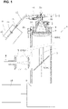
- FIG. 1 shows a first embodiment (vertical irradiation) of a soldering device 1
- FIG. 11 shows a second embodiment (inclined irradiation) thereof.
- difference from the first embodiment will be mainly described, and for the same matter, description in the first embodiment is applied to description in the second embodiment and the same matter will not be described repeatedly.
- the soldering device 1 includes a semiconductor laser or a laser oscillator (not shown) that outputs a laser beam L; a support base 2 on which a printed board 40 is set; an emission head 3 that is provided under the printed board 40 and applies a laser beam L outputted from the semiconductor laser or the like to a soldering point (in the present invention, a part on the lower surface side of a land 42 of the printed board 40, this part is referred to as land-lower-surface part 42k) provided on a lower surface 40k of the printed board 40; a laser controller (not shown) for controlling the semiconductor laser or the like; a wire solder feeding portion 11 for feeding wire solder 15 to the soldering point; a monitor 10 that displays a solder state; and a control device (not shown) that automatically controls the entire soldering device 1 in accordance with a set program.
- a semiconductor laser or a laser oscillator not shown
- an emission head 3 that is provided
- the printed board 40 is a board on which a large number of and various kinds of electronic components 50 are to be mounted.
- the printed board 40 is not limited to a single-layer board but may be a multilayer board.
- a case where the printed board 40 is a single-layer board will be described as a representative example.
- a board body (insulating substrate) 40a of the printed board 40 has multiple through holes penetrating from an upper surface 40j thereof to the lower surface 40k.
- This copper plating layer part is the land 42, and a hole penetrating through the land 42 is the through hole 41.
- the ring-shaped copper plating layers at the opening peripheral edges of the land 42 are defined as land-upper-surface part 42j and land-lower-surface part 42k, and the copper plating layer on the inner circumferential surface of the through hole, connecting the land upper and lower surface parts 42j and 42k, is defined as conduction part 43.
- a large number of and various kinds of electronic components 50 are mounted at the upper surface 40j of the printed board 40, and a lead 52 of each electronic component 50 is inserted into the through hole 41.
- the inserted lead 52 passes through the through hole 41 and slightly protrudes from the lower surface 40k.
- the inserted lead 52 is to be soldered over the entire land 42 of the printed board 40 by a method described later.
- the leads 52 may have various sectional shapes such as a circular shape or a quadrangular shape in accordance with the various kinds of electronic components 50.
- the protruding lead 52 and the land-lower-surface part 42k are irradiated with the laser beam L, whereby the wire solder 15 fed to the irradiated part is melted and the lead 52 and the land 42 are soldered ( FIG. 8 ).
- the relationship between the copper plating layer (conduction part 43) that is the inner circumferential part of the land 42, and the lead 52 of the electronic component 50, is as follows.
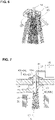
- the diameter of the lead 52 is slightly smaller than the inner diameter of the conduction part 43, and a gap S between the conduction part 43 and the lead 52 is slight (e.g., around 0.1 mm) and is a gap that allows melted solder 15m to penetrate by capillary action as described later ( FIG. 3 ).
- the emission head 3 of the soldering device 1 is placed under the printed board 40 placed on the support base 2 of the soldering device 1.
- the land-lower-surface part 42k at the soldering point on the lower surface 40k of the printed board 40 is exposed downward from an opening part of the support base 2.
- the emission head 3 may be placed vertically to the printed board 40 so that the emission port 4 of the emission head 3 faces the lower surface 40k of the printed board 40 (first embodiment), and as shown in FIG. 11 , the emission head 3 may be placed so as to be inclined relative to the printed board 40 (second embodiment).
- the outer shape of the emission head 3 is substantially a cylindrical shape or a polygonal tube shape, and a laser introducing tube portion 5 protrudes orthogonally from the side surface of the emission head 3.
- An optical fiber 8 leading to the semiconductor laser or the like is connected to the laser introducing tube portion 5, so that the laser beam L outputted from the semiconductor laser or the like passes through the optical fiber 8 and is introduced into the emission head 3.
- a semi-transparent mirror 6a for changing the direction of the introduced laser beam L and optical components 6b such as optical lenses for focusing the laser beam L to a predetermined diameter on the land-lower-surface part 42k at the soldering point, are mounted at certain positions on an optical path to the emission port 4.
- the emission port 4 is provided at the upper end of the emission head 3 and faces the lower surface 40k of the printed board 40.
- the laser beam L entering the emission head 3 passes through an internal optical system 6 and then is emitted from the emission port 4 toward the land-lower-surface part 42k at the soldering point P.
- protection glass 7 transparent over the entire area, and center-part-output limiting glass 7a provided if necessary as described later, are mounted.
- the first type has the same output level over an entire area of the transverse section at the land-lower-surface part 42k, which is the irradiation surface ( FIG. 1 , FIG. 9(b) ), and the second type has a double ring structure having a center part L1 and an outer peripheral part L2 formed concentrically therearound and surrounding the center part L1 ( FIG. 2 , FIG. 10(b) ).
- the second type is set such that the outer peripheral part L2 has a higher output level than the center part L1.
- the laser beam L having the double ring structure of the second type is shown, and the center part L1 is shown as a shaded part.
- FIG. 10 a uniform output laser beam L set in an inclined state is shown. However, without limitation thereto, a non-uniform output laser beam is also used (not shown).
- the laser beam L has a uniform output level as in the first type
- a setting for lowering the output level of the center part L1 of the laser beam L is not made in the optical system 6, and therefore the laser beam L entering the emission head 3 passes as it is through the optical system 6 and the protection glass 7 of the emission head 3, thus having the same output level over the entire area of the transverse section at the irradiation surface as described above.
- the output level in this case is schematically shown in FIG. 9(b) .
- the irradiation range of the uniform output laser beam L is set to be the land-lower-surface part 42k in both of a case of vertical irradiation and a case of inclined irradiation, as described later.
- the output level of the laser beam L is controlled so as not to cause "lead burn", as described later.
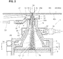
- a member (not shown) for limiting the output level of the center part L1 of the laser beam L is provided at any position in the optical system 6 of the emission head 3, or as shown in FIG. 2 , the center-part-output limiting glass 7a having an output limiting area 7b for limiting the output level of the center part of the laser beam L is provided along the upper surface of the protection glass 7.
- the output level of the outer peripheral part L2 is 100
- the output level of the center part L1 is limited to a range of 40 to 60. Change of the output level is performed by replacing the center-part-output limiting glass 7a with other ones having various limitation values.
- the diameter of the center part L1 of the non-uniform output laser beam L is, at maximum, equal to the inner diameter of the through hole 41.
- the output level of the center part L1 applied to the protruding end of the lead 52 inserted through the through hole 41 becomes considerably lower than the surrounding outer peripheral part L2, so that "lead burn” does not occur even if the laser beam of the center part L1 having a low output level is continuously applied during a preheating step.
- the non-uniform output laser beam L there are a case where the laser beam L is set vertically and a case where the laser beam L is set in an inclined state.
- the outer peripheral part L2 thereof is a ring-shaped area obtained by subtracting, from the irradiation area of the laser beam L covering the land-lower-surface part 42k at the soldering point P, the center part L1 located at a center part of the irradiation area.
- the land-lower-surface part 42k of the printed board 40 has a circular shape, the laser beam L is applied over the entire land-lower-surface part 42k, and the maximum diameter position of the laser beam L is at the outer edge of the land-lower-surface part 42k.
- the shape of the land-lower-surface part 42k of the printed board 40 is not limited to a circular shape but may be various shapes. For example, in a case of an oblong shape, the range of the laser beam L corresponds to the short-side width of the oblong shape so that the laser beam L is not applied to the board body 40a, which is an insulating material.
- the irradiated surface has an elliptic shape, and therefore the laser beam L is applied in such a range that the major-axis side thereof does not protrude out of the land-lower-surface part 42k.
- a protection nozzle 20 is mounted to the emission port 4 of the emission head 3.
- the protection nozzle 20 has a hollow conical shape extending upward from the emission port 4, and a tubular nozzle port 21 is fitted to the tip part of the protection nozzle 20.
- the nozzle port 21 is made of a heat resistant material, e.g., ceramic.
- the nozzle port 21 has a pass hole 22 through which the laser beam L narrowed to be thin passes. The diameter of the pass hole 22 is slightly larger than the diameter of the laser beam L passing therethrough.
- a heating gas supply pipe 26 is connected to a base part of the protection nozzle 20 near the emission port 4 of the emission head 3, and high-temperature gas is constantly supplied to the inside.
- the high-temperature gas may be normal air or an inert gas such as nitrogen gas.
- the melting point of the wire solder 15 varies depending on the composition thereof, and in a case of leadfree solder, is approximately 220°C.
- the temperature of the high-temperature gas supplied to the protection nozzle 20 is such a temperature that can preheat the through hole 41 and the surrounding area, and the wire solder 15 fed thereto (e.g., 110°C to 150°C) and that does not exceed, at maximum, a temperature shortly below the melting point of the wire solder 15.
- the high-temperature gas is blown out upward from the pass hole 22, as a hot wind N.
- the inside of the protection nozzle 20 is constantly kept at a positive pressure by the high-temperature gas being supplied. Therefore, a foreign material (fine product) C does not enter the inside of the protection nozzle 20 from the pass hole 22.
- the protection nozzle 20 may be a mere conical hollow tube body (not shown).
- FIG. 2 and FIG. 3 an example in which the protection nozzle 20 is provided with a conical guide wall 24 along the inner circumferential surface thereof, is shown.
- the guide wall 24 forms a guide flow path G that guides flow of the hot wind N, between the inner circumferential surface of the protection nozzle 20 and the guide wall 24. If the gap between the inner circumferential surface and the guide wall 24 is gradually narrowed toward the pass hole 22, the flow speed of the hot wind N flowing through the guide flow path G can be increased. It is noted that the guide wall 24 covers the upper surface of the protection glass 7 (or center-part-output limiting glass 7a) and thus prevents the high-temperature gas blown into the protection nozzle 20 from contacting with the protection glass (or center-part-output limiting glass 7a).
- the heating gas supply pipe 26 may be connected perpendicularly to the base part of the protection nozzle 20. Alternatively, as shown in FIG. 4 , the heating gas supply pipe 26 may be connected in the tangent direction of the inner circumferential surface of the protection nozzle 20 so that the blown high-temperature gas forms a helical flow along the inner circumferential surface (or guide flow path G) inside the protection nozzle 20 and is blown out as a thin helical-flow hot wind N from the pass hole 22.
- the hot wind N as a helical flow, the directionality of the blow-out direction is enhanced, and thus the lead 52 and the land 42 located near the pass hole 22 can be intensively preheated.
- preheating by the hot wind N from the underside of the printed board 40 is disclosed. However, in addition thereto, preheating by a hot wind N from the upper side of the printed board 40 may be further performed.
- an exhaust duct 30 is provided so as to surround the circumference of the pass hole 22 of the protection nozzle 20.
- the exhaust duct 30 is provided as necessary and is not essential.
- an example in which the exhaust duct 30 is provided is shown.
- the exhaust duct 30 is a dish-like member and has an opening 31 at the center thereof.
- An upper end part (nozzle port 21) of the protection nozzle 20 is inserted into the opening 31.
- An upper edge 30a of the exhaust duct 30 and an upper end of the nozzle port 21 of the protection nozzle 20 are located below the lower surface 40k of the printed board 40 located upward, and are provided with a gap from the lower surface 40k.
- This gap is formed to have a width greater than the protruding interference of the lead 52 from the lower surface 40k of the printed board 40.
- An exhaust tube portion 32 is provided to the side wall of the exhaust duct 30, and an exhaust pipe 33 is connected to the exhaust tube portion 32.
- the exhaust pipe 33 constantly sucks and discharges air in the exhaust duct 30.
- the hot wind N blown out from the pass hole 22 of the nozzle port 21 of the protection nozzle 20 hits the lower surface 40k of the printed board 40 (at the time of soldering, the lead 52, the through hole 41, and the surrounding area), to preheat the hit part, and then flows into the exhaust duct 30. Then, most or the entirety of the hot wind N flows into the exhaust pipe 33.
- a ring-shaped cooling pipe 35 is provided around the outer circumference of a trunk portion of the protection nozzle 20, and a cooling water supply pipe 36 and a cooling water discharge pipe 37 are attached to the cooling pipe 35. Cooling water is supplied from the cooling water supply pipe 36, circulates through the cooling pipe 35, and returns to the cooling water discharge pipe 37, so as to be discharged therethrough. Thus, the protection nozzle 20 is cooled by the cooling water.
- the wire solder feeding portion 11 is for feeding the wire solder 15 wound around, for example, a pulley (not shown), toward the land-lower-surface part 42k of the land 42 at the soldering point, on a required amount basis as necessary.
- the wire solder feeding portion 11 has a guide nozzle 12 extending to a position close to the land-lower-surface part 42k at the soldering point.
- the wire solder feeding portion 11 receives a control command such as a feeding timing and a feeding amount of the wire solder 15 from the control device, and sends the wire solder 15 through the guide nozzle 12 in accordance with the control command.
- the sent wire solder 15 is fed to a position contacting with the lead 52 or the land-lower-surface part 42k at the soldering point, or a position contacting with both of them. At this time, as described later, the tip of the fed wire solder 15 is exposed to only the hot wind N or to the hot wind N and the laser beam L, so as to be preheated, but since the heating temperature of the hot wind N and the output level of the laser beam L are low, the wire solder 15 is not melted at this point of time.
- the sectional shape of the wire solder 15 is a circular shape.
- the wire solder 15 may be compressed to be flattened by a pair of upper and lower press rollers 13 before inserted into the guide nozzle 12 so that flat parts 16a, 16b are formed on the front and back sides of the wire solder 15.
- a guide hole of the guide nozzle 12 also has a flattened rectangular shape corresponding to the wire solder 15, and the flattened wire solder 15 is fed such that one flat part 16a thereof is along the lower surface 40k of the printed board 40.
- the laser beam L is applied to the flat part 16b on the opposite side, so that the laser beam L is less scattered and is readily absorbed by the flattened wire solder 15.
- an oscillation control command is issued from a laser controller.
- the semiconductor laser or the like emits the laser beam L with a predetermined output and an irradiation time, and the emission head 3 emits the laser beam L vertically or obliquely upward from the underside toward the land-lower-surface part 42k at the soldering point. Then, the wire solder 15 is fed thereto.
- feeding of the wire solder 15 is completed before the (uniform/non-uniform output) laser beam L having the output level (B) is emitted.
- the wire solder 15 is heated and melted by the laser beam L and soldering is performed.
- a CCD camera 9 is attached such that the optical axis thereof is coaxial with the laser beam L, and the soldering point can be imaged through the emission port 4 by the CCD camera 9.
- the image of the soldering point taken by the CCD camera 9 is displayed on the monitor 10 via the control device.
- the CCD camera 9 Before soldering, it is possible to use the CCD camera 9 for performing aiming adjustment of the laser beam L with respect to the land-lower-surface part 42k at the soldering point while viewing the image displayed on the monitor 10, or during soldering work, it is possible to observe the state of soldering work at the soldering point by the CCD camera 9.
- Embodiments of the laser soldering method according to the present invention include the first embodiment ( FIG. 1 to FIG. 8 : vertical arrangement) and the second embodiment ( FIG. 11 : inclined arrangement).
- the first embodiment is a case where the emission head 3 is placed vertically to the lower surface 40k of the printed board 40
- the second embodiment is a case where the emission head 3 is placed so as to be inclined by an inclination angle ⁇ relative to a line vertical to the lower surface 40k of the printed board 40.
- the inclination angle ⁇ is 50° ⁇ 10°.
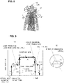
- FIG. 9(a) and FIG. 10(a) there are a case of changing the laser output in stages, i.e., a first output procedure ((1), (2), (3), (4), (5), (6), (7)), a case of changing the laser output continuously, i.e., a second output procedure ((20), (4), (21)), and a case of performing output in a rectangular manner, i.e., a third output procedure ((10), (4), (5)).
- a first output procedure (1), (2), (3), (4), (5), (6), (7)
- a second output procedure ((20), (4), (21)
- a case of performing output in a rectangular manner i.e., a third output procedure ((10), (4), (5)).
- the output is set at two stages of a level (A) and a level (B), but without limitation thereto, may be set in any multiple stages.
- the level (A) is an output level that does not cause "lead burn” (such an output that the temperature at the irradiated part is increased to about 110°C to 150°C)
- the level (B) is an output level that enables "soldering" (not lower than the solder melting temperature).
- the first to third output procedures are determined on the basis of the condition of a soldering target, and the switching timing therefor is determined by software inputted to a controller or determined through detection for a measurement temperature at the soldering point by a radiation thermometer (not shown).
- preheating for the soldering point P there are two cases where preheating is performed by only the hot wind N without the laser beam L and where preheating is performed through cooperation using the hot wind N and the laser beam L.
- soldering work in the first embodiment (vertical) using the uniform output laser beam L or the non-uniform output laser beam L will be described ( FIG. 1 , FIG. 2 to FIG. 8 , FIG. 9 , FIG. 10 ).
- the optical axis of the emission head 3 is aligned with the center of the through hole 41 as the soldering target of the printed board 40 placed on the support base 2 of the soldering device 1.
- the emission head 3 is provided under the printed board 40 vertically to the printed board 40.
- the above optical axis alignment is automatically performed through image processing or may be manually adjusted via the monitor 10.
- the hot wind N blown out from the pass hole 22 is blown around the land-lower-surface part 42k at the soldering point P, thereby heating this part.
- the laser beam L is not being emitted.
- Preheating step (cooperative preheating using hot wind N and laser beam L)
- the pass hole 22 is located directly under the land-lower-surface part 42k at the soldering point P.
- the hot wind N blown out from the pass hole 22 has been preheating the through hole 41 and the surrounding area, and the lead 51 inserting through the through hole 41.
- the uniform or non-uniform output laser beam L is emitted toward the lead 52 and the land-lower-surface part 42k at the soldering point (see (1) in FIG. 9(a) and FIG. 10(a) ).
- the output level thereof is high, the lead 52 is overheated, thus causing a "lead burn” phenomenon in which the color of the irradiated part is changed. Therefore, at this time, the output is limited to such a degree (indicated by level (A)) that does not cause a "lead burn” phenomenon.
- the preheating temperature by the hot wind N and the laser output is a temperature (e.g., 110 to 150°C) lower than the melting point of the used wire solder 15.
- the output level of the outer peripheral part L2 is set at (A) so that the wire solder 15 fed to the soldering point P is not melted. Since the output level of the center part L1 is (B) and thus is lower than the output level of the outer peripheral part L2, it suffices that the output level of the outer peripheral part L2 is managed.
- the hot wind N In a case where the hot wind N is not a helical flow but is blown out vertically toward the through hole 41 from the pass hole 22, as described above, the hot wind N preheats the surrounding area around the land-lower-surface part 42k, the inner circumferential surface of the through hole 41, and the lead 52 inserted through the through hole 41, and further, the hot wind N passing through the through hole 41 and coming around to the upper surface 40j side of the printed board 40 preheats the land-upper-surface part 42j and the surrounding area. This also applies to the soldering procedure described later.
- the blowing-out directionality is enhanced as compared to the case of merely blowing out as described above and the hot wind N is blown into the through hole 41, whereby the lead 52 present at the center of the through hole 41 is mainly preheated.
- a major part of the hot wind N hitting the through hole 41 including the lead 52 directly flows to the surrounding area, to preheat the land-lower-surface part 42k.
- the rest of the hot wind N passing through the through hole 41 preheats the land-upper-surface part 42j and the surrounding area. This also applies to the soldering procedure described later.
- a period for the preheating is determined by time setting from the finish time of optical axis alignment or measurement for the temperature at the preheated part using a radiation thermometer.
- the operation is switched to a soldering step along with finish of the preheating step.
- the output thereof is switched to the level (B).
- the output for the outer peripheral part L2 is switched to the level (B).
- Feeding of the wire solder 15 is performed before the output of the laser beam L (or outer peripheral part L2) is switched to the level (B).
- the laser beam L (or outer peripheral part L2) at the level (B) is outputted thereto and the wire solder 15 is rapidly melted from the irradiated part including the contact part.
- the wire solder 15 changes from a solid phase to a liquid phase, latent heat is needed and therefore the temperature of the melted solder 15m is slightly lowered, but the melted solder 15m is kept in a liquid phase by heat from the laser beam L.
- the wire solder 15 is continuously fed to the soldering point P until just before soldering is finished, and thus is continuously melted.
- the amount of the melted solder 15m increases through feeding of the wire solder 15 as described above.
- the melted solder 15m spreads over the lead 52 and the land-lower-surface part 42k, to connect both parts, and meanwhile, passes through the gap S between both preheated parts by a "capillary action", to rise toward the upper surface 40j of the printed board 40, so that the melted solder 15m spreads over the land-upper-surface part 42j of the printed board 40 and the lead 52, and fills the gap S therebetween.
- the melted solder 15m exhibits the above "capillary action" while being kept in a liquid phase without being solidified ( FIG. 6 ).
- the sectional shape of the wire solder 15 is a circular shape
- the laser beam L is applied to the outer surface thereof
- the laser beam L is scattered around and thus the energy absorption efficiency is deteriorated.
- the wire solder 15 is compressed to be flattened by the press rollers 13 before feeding of the wire solder, when the laser beam L is applied vertically to the one flat part 16b, the scattering amount therearound is reduced, and the wire solder 15 is melted faster than the wire solder 15 having a circular shape.
- the fume and the other fine products C blown away by the hot wind N are received by the exhaust duct 30 provided so as to surround the periphery of the protection nozzle 20 and kept at a negative pressure therein, and then are discharged through the exhaust pipe 33 to the outside.
- the inside of the exhaust duct 30 is constantly kept at a negative pressure by discharge through the exhaust pipe 33 as described above, and the outer air flows inward from a gap between the printed board 40 and the upper edge of the exhaust duct 30. Therefore, leakage of the fine products C to the outside of the exhaust duct 30 during the soldering work is significantly suppressed. Thus, the surrounding environment is prevented from being contaminated by soldering from the underside of the printed board 40.
- the uniform output laser beam L having the high output level (B) is continuously applied to the tip of the lead 51, but heat provided to the lead 51 by the laser beam L is absorbed by the wire solder 15m being melted continuously. Thus, temperature increase is suppressed and "lead burn" does not occur.
- the output level of the center part L1 at this time is such a low level (A) that the wire solder 15 is not melted. Therefore, "lead burn” does not occur even when the laser beam L is continuously applied to the tip of the lead 51 as described above.
- the laser beam L is stopped in this state (procedure (5)). Then, the emission head 3 is moved to the next soldering point P, and the preheating and the soldering work described above are performed at the movement destination.
- solidified solder 15h having a conical shape as shown in FIG. 8 is formed on the front and back sides of the printed board 40.
- Second output procedure (shown by thin dashed-dotted lines in FIG. 9(a) and FIG. 10(a): (20), (4), (21))
- Preheating step using hot wind and laser beam in combination
- a preheating step heating by the hot wind N and heating by the uniform output or non-uniform output laser beam L are performed at the soldering point P. After optical axis alignment is completed, the output level of the laser beam L is continuously increased until start of soldering. At the time when soldering is started, the output level of the uniform output laser beam L or the outer peripheral part L2 of the non-uniform output laser beam L is (B). For the matters other than the above, the description of the first output procedure is applied.
- the wire solder 15 is fed and soldering is performed. Therefore, the first output procedure is applied.
- the output of the laser beam L is gradually reduced.
- the melted solder 15m can be prevented from being rapidly cooled, and strain in the solidified solder 15h is relaxed.
- Preheating step preheating by hot wind alone
- soldering is started.
- the wire solder 15 is fed and soldering is performed. Therefore, the first output procedure is applied.
- the laser beam L is stopped at the same time as soldering is finished.
- the output level is lowered in stages. This step is also the same as that in the first output procedure, and therefore the first output procedure is applied. (As a matter of course, gradual cooling in the post-heating step in the second output procedure may be used.) For the matters other than the above, the description of the first output procedure is applied.
- the emission head 3 is provided so as to be inclined relative to the vertical line of the printed board 40. Therefore, in this case, the optical axis of the emission head 3 is aligned with the protrusion base of the lead 51 protruding from the through hole 41. In the second embodiment, establishing this state is defined as "optical axis alignment".
- the wire solder 15 is fed from such a direction as not to be hidden by the lead 52 and as not to interfere with the tip of the protection nozzle 20.
- the hidden part is shown as a shaded part ( FIG. 12 ).
- the wire solder 15 is fed at an angle of 140° with respect to the optical axis of the laser beam L. As a matter of course, the angle is not limited thereto.
- the irradiated surface forms an elliptic shape ( FIG. 12 ).
- the output level on the irradiated surface is not entirely uniform, but is high at the center part and slightly lower at the outer edge part than at the center part, for an optical reason.
- the protruding part of the lead 52 is irradiated with the laser beam L having the high level (B), but as described above, even in the case of the uniform output laser beam L, the outer peripheral part thereof has a lower output level, and therefore "lead burn" does not occur as long as the protruding part is exposed only for such a short period before the covering.
- the output level of the center part L1 is lower than the output level of the outer peripheral part L2, as described above. Since the protruding part of the lead 52 is exposed to the center part L1 having the lower output level, as a matter of course, "lead burn” does not occur. The wire solder 15 is melted by being exposed to the outer peripheral part L2 having the higher output level.
Landscapes
- Engineering & Computer Science (AREA)
- Mechanical Engineering (AREA)
- Physics & Mathematics (AREA)
- Optics & Photonics (AREA)
- Manufacturing & Machinery (AREA)
- Plasma & Fusion (AREA)
- Microelectronics & Electronic Packaging (AREA)
- Electric Connection Of Electric Components To Printed Circuits (AREA)
Applications Claiming Priority (1)
| Application Number | Priority Date | Filing Date | Title |
|---|---|---|---|
| PCT/JP2019/037997 WO2021059456A1 (ja) | 2019-09-26 | 2019-09-26 | レーザー式ハンダ付け方法とその装置 |
Publications (2)
| Publication Number | Publication Date |
|---|---|
| EP4013196A1 true EP4013196A1 (de) | 2022-06-15 |
| EP4013196A4 EP4013196A4 (de) | 2022-10-12 |
Family
ID=72047783
Family Applications (1)
| Application Number | Title | Priority Date | Filing Date |
|---|---|---|---|
| EP19947320.8A Withdrawn EP4013196A4 (de) | 2019-09-26 | 2019-09-26 | Laserlötverfahren und -vorrichtung |
Country Status (7)
| Country | Link |
|---|---|
| US (1) | US20220320811A1 (de) |
| EP (1) | EP4013196A4 (de) |
| JP (1) | JP6744686B1 (de) |
| KR (1) | KR102496836B1 (de) |
| CN (1) | CN114503791A (de) |
| TW (1) | TWI740428B (de) |
| WO (1) | WO2021059456A1 (de) |
Families Citing this family (14)
| Publication number | Priority date | Publication date | Assignee | Title |
|---|---|---|---|---|
| DE102020113124A1 (de) * | 2020-05-14 | 2021-11-18 | Eberspächer catem Hermsdorf GmbH & Co. KG | PTC-Heizzelle und Verfahren zu deren Herstellung |
| KR102591564B1 (ko) * | 2021-09-15 | 2023-10-19 | 엘에스이브이코리아 주식회사 | 레이저 솔더링 시스템 |
| TWI781778B (zh) * | 2021-09-30 | 2022-10-21 | 台達電子工業股份有限公司 | 焊接系統及吹氣的自動控制方法 |
| CN115890066B (zh) * | 2021-09-30 | 2025-10-17 | 台达电子工业股份有限公司 | 焊料供应装置、焊接系统及吹气的自动控制方法 |
| TWI805387B (zh) * | 2021-09-30 | 2023-06-11 | 台達電子工業股份有限公司 | 焊料供應裝置、焊接系統及吹氣的自動控制方法 |
| DE102022120336A1 (de) * | 2021-10-06 | 2023-04-06 | Pac Tech - Packaging Technologies Gmbh | Lasergestützte Lötvorrichtung und Lotaufbringungsmaschine |
| CN114951994B (zh) * | 2022-05-25 | 2023-08-04 | 武汉凌云光电科技有限责任公司 | 一种激光恒温焊接控制系统和方法 |
| DE102022205845A1 (de) | 2022-06-08 | 2023-12-14 | Robert Bosch Gesellschaft mit beschränkter Haftung | Bearbeitungskopf für ein Laserbearbeitungssystem, Laserbearbeitungssystem, Verfahren zur Änderung der Fokuslage eines Bearbeitungskopfes für ein Laserbearbeitungssystem, Computerprogramm |
| CN115224561B (zh) * | 2022-07-15 | 2025-07-29 | 西安微电子技术研究所 | 一种用于板间连接器热风整体吹焊的均热型装置 |
| CN115411145B (zh) * | 2022-09-07 | 2025-07-22 | 常州时创能源股份有限公司 | 一种太阳能电池片的焊接装置及方法 |
| CN116393699A (zh) * | 2023-03-21 | 2023-07-07 | 上海汉邦联航激光科技有限公司 | 3d打印设备及其窗口镜安装结构 |
| CN116275352B (zh) * | 2023-05-22 | 2023-07-21 | 云泰智能科技(天津)有限责任公司 | 一种印刷电路板的焊接装置 |
| CN116727852A (zh) * | 2023-07-04 | 2023-09-12 | 大族激光科技产业集团股份有限公司 | 激光焊接方法、设备及焊嘴 |
| CN117415456A (zh) * | 2023-11-13 | 2024-01-19 | 湖北省轻工业科学研究设计院有限公司 | 一种用于pcb线束激光焊接的装置 |
Family Cites Families (15)
| Publication number | Priority date | Publication date | Assignee | Title |
|---|---|---|---|---|
| US4801352A (en) * | 1986-12-30 | 1989-01-31 | Image Micro Systems, Inc. | Flowing gas seal enclosure for processing workpiece surface with controlled gas environment and intense laser irradiation |
| JPH04237557A (ja) * | 1991-01-17 | 1992-08-26 | Matsushita Electric Ind Co Ltd | はんだ付け方法 |
| JPH0623530A (ja) * | 1992-04-28 | 1994-02-01 | Omron Corp | レーザ照射型ハンダ接合装置 |
| JPH06169167A (ja) * | 1992-11-10 | 1994-06-14 | Matsushita Electric Ind Co Ltd | 光ビームによる上向きはんだ付け方法 |
| JPH07124781A (ja) * | 1993-10-28 | 1995-05-16 | Hitachi Constr Mach Co Ltd | レーザ加工方法及び加工装置 |
| JP3380319B2 (ja) * | 1994-02-01 | 2003-02-24 | 株式会社田中製作所 | レーザ切断方法およびレーザ切断ノズル |
| JP2001198670A (ja) * | 2000-01-17 | 2001-07-24 | Japan Unix Co Ltd | レーザー式はんだ付け方法及び装置 |
| JP2001232460A (ja) * | 2000-02-24 | 2001-08-28 | Matsushita Electric Ind Co Ltd | 光ビーム加熱装置および光ビームはんだ付け方法 |
| JP3590319B2 (ja) * | 2000-03-10 | 2004-11-17 | 株式会社ジャパンユニックス | ガス噴射式はんだ付け方法及び装置 |
| JP2008114275A (ja) * | 2006-11-07 | 2008-05-22 | Takeji Arai | レーザ加工ヘッド及びレーザ加工方法 |
| JP5148118B2 (ja) * | 2007-01-15 | 2013-02-20 | 株式会社ジャパンユニックス | レーザー式はんだ付け装置 |
| JP5874452B2 (ja) * | 2012-03-08 | 2016-03-02 | アイシン精機株式会社 | 基板、ハンダ付け装置およびハンダ付け方法 |
| JP5974854B2 (ja) * | 2012-11-26 | 2016-08-23 | 富士通株式会社 | はんだ接合装置及びはんだ接合方法 |
| JP5910784B1 (ja) * | 2015-09-11 | 2016-04-27 | 千住金属工業株式会社 | 噴流ノズル及び噴流はんだ付け装置 |
| JP6447782B2 (ja) * | 2016-11-22 | 2019-01-09 | 千住金属工業株式会社 | はんだ付け方法 |
-
2019
- 2019-09-26 US US17/753,456 patent/US20220320811A1/en not_active Abandoned
- 2019-09-26 CN CN201980100692.8A patent/CN114503791A/zh active Pending
- 2019-09-26 KR KR1020227012527A patent/KR102496836B1/ko active Active
- 2019-09-26 JP JP2020500907A patent/JP6744686B1/ja active Active
- 2019-09-26 EP EP19947320.8A patent/EP4013196A4/de not_active Withdrawn
- 2019-09-26 WO PCT/JP2019/037997 patent/WO2021059456A1/ja not_active Ceased
-
2020
- 2020-03-26 TW TW109110127A patent/TWI740428B/zh active
Also Published As
| Publication number | Publication date |
|---|---|
| US20220320811A1 (en) | 2022-10-06 |
| KR20220053039A (ko) | 2022-04-28 |
| JPWO2021059456A1 (ja) | 2021-10-07 |
| EP4013196A4 (de) | 2022-10-12 |
| CN114503791A (zh) | 2022-05-13 |
| TWI740428B (zh) | 2021-09-21 |
| JP6744686B1 (ja) | 2020-08-19 |
| KR102496836B1 (ko) | 2023-02-07 |
| WO2021059456A1 (ja) | 2021-04-01 |
| TW202112478A (zh) | 2021-04-01 |
Similar Documents
| Publication | Publication Date | Title |
|---|---|---|
| EP4013196A1 (de) | Laserlötverfahren und -vorrichtung | |
| JP5294916B2 (ja) | レーザはんだ付け装置 | |
| CN114505553B (zh) | 激光锡焊方法、装置及系统 | |
| KR101187940B1 (ko) | 전자 부품의 리페어 장치, 리페어 방법, 및 리페어용 열전달 캡 부재 | |
| JP3720681B2 (ja) | レーザー式はんだ付け方法及び装置 | |
| CN101583456B (zh) | 激光焊接装置 | |
| JPH03193282A (ja) | Smd―要素のためのレーザはんだ付け装置 | |
| TWI775845B (zh) | 雷射軟焊方法及裝置 | |
| JP3622714B2 (ja) | 加工方法 | |
| CN101370359B (zh) | 焊料修复设备及修复焊料的方法 | |
| WO2010018680A1 (ja) | 光ビームを用いた表面実装機 | |
| CN110280862A (zh) | 一种器件管脚的焊接系统及其方法 | |
| US5741410A (en) | Apparatus for forming spherical electrodes | |
| JP2006156446A (ja) | 半田付け方法及び装置 | |
| US20090039525A1 (en) | Method of Welding Together at Least Two Stacked Members | |
| JPH10335806A (ja) | 回路モジュールの製造方法及びその装置 | |
| HK40066539A (zh) | 激光式软釺焊方法及激光式软釺焊装置 | |
| CN107498140B (zh) | 激光同轴钎焊装置及激光焊接方法 | |
| JP5056590B2 (ja) | 半田付け方法及び装置 | |
| JP2003204149A (ja) | 電子部品のはんだ付け方法及びその装置 | |
| JP7447387B2 (ja) | 回路基板に電子部品をはんだ付けするための方法及び装置、コンピュータプログラム製品、並びにコンピュータ可読媒体 | |
| US6680457B2 (en) | Reflowing of solder joints | |
| KR20250038633A (ko) | 솔더링 위치가 조절되는 레이저 솔더링 장치 및 이를 포함하는 솔더링 방법 | |
| JP2003060338A (ja) | 半導体部品実装装置およびその半導体部品実装方法 | |
| JP2024048115A (ja) | レ-ザーハンダ付け装置 |
Legal Events
| Date | Code | Title | Description |
|---|---|---|---|
| STAA | Information on the status of an ep patent application or granted ep patent |
Free format text: STATUS: THE INTERNATIONAL PUBLICATION HAS BEEN MADE |
|
| PUAI | Public reference made under article 153(3) epc to a published international application that has entered the european phase |
Free format text: ORIGINAL CODE: 0009012 |
|
| STAA | Information on the status of an ep patent application or granted ep patent |
Free format text: STATUS: REQUEST FOR EXAMINATION WAS MADE |
|
| 17P | Request for examination filed |
Effective date: 20220308 |
|
| AK | Designated contracting states |
Kind code of ref document: A1 Designated state(s): AL AT BE BG CH CY CZ DE DK EE ES FI FR GB GR HR HU IE IS IT LI LT LU LV MC MK MT NL NO PL PT RO RS SE SI SK SM TR |
|
| A4 | Supplementary search report drawn up and despatched |
Effective date: 20220908 |
|
| RIC1 | Information provided on ipc code assigned before grant |
Ipc: B23K 101/42 20060101ALN20220902BHEP Ipc: B23K 26/60 20140101ALI20220902BHEP Ipc: B23K 26/16 20060101ALI20220902BHEP Ipc: B23K 26/14 20140101ALI20220902BHEP Ipc: B23K 26/03 20060101ALI20220902BHEP Ipc: B23K 1/20 20060101ALI20220902BHEP Ipc: B23K 1/005 20060101ALI20220902BHEP Ipc: B23K 1/00 20060101ALI20220902BHEP Ipc: H05K 3/34 20060101AFI20220902BHEP |
|
| DAV | Request for validation of the european patent (deleted) | ||
| DAX | Request for extension of the european patent (deleted) | ||
| STAA | Information on the status of an ep patent application or granted ep patent |
Free format text: STATUS: THE APPLICATION HAS BEEN WITHDRAWN |
|
| 18W | Application withdrawn |
Effective date: 20230208 |