EP4024629A1 - Beleuchtungsvorrichtung und ranging-vorrichtung - Google Patents
Beleuchtungsvorrichtung und ranging-vorrichtung Download PDFInfo
- Publication number
- EP4024629A1 EP4024629A1 EP20876299.7A EP20876299A EP4024629A1 EP 4024629 A1 EP4024629 A1 EP 4024629A1 EP 20876299 A EP20876299 A EP 20876299A EP 4024629 A1 EP4024629 A1 EP 4024629A1
- Authority
- EP
- European Patent Office
- Prior art keywords
- light
- emitting sections
- emitting
- multiple pieces
- lighting device
- Prior art date
- Legal status (The legal status is an assumption and is not a legal conclusion. Google has not performed a legal analysis and makes no representation as to the accuracy of the status listed.)
- Pending
Links
Images






Classifications
-
- G—PHYSICS
- G01—MEASURING; TESTING
- G01S—RADIO DIRECTION-FINDING; RADIO NAVIGATION; DETERMINING DISTANCE OR VELOCITY BY USE OF RADIO WAVES; LOCATING OR PRESENCE-DETECTING BY USE OF THE REFLECTION OR RERADIATION OF RADIO WAVES; ANALOGOUS ARRANGEMENTS USING OTHER WAVES
- G01S7/00—Details of systems according to groups G01S13/00, G01S15/00, G01S17/00
- G01S7/48—Details of systems according to groups G01S13/00, G01S15/00, G01S17/00 of systems according to group G01S17/00
- G01S7/481—Constructional features, e.g. arrangements of optical elements
- G01S7/4814—Constructional features, e.g. arrangements of optical elements of transmitters alone
- G01S7/4815—Constructional features, e.g. arrangements of optical elements of transmitters alone using multiple transmitters
-
- G—PHYSICS
- G01—MEASURING; TESTING
- G01S—RADIO DIRECTION-FINDING; RADIO NAVIGATION; DETERMINING DISTANCE OR VELOCITY BY USE OF RADIO WAVES; LOCATING OR PRESENCE-DETECTING BY USE OF THE REFLECTION OR RERADIATION OF RADIO WAVES; ANALOGOUS ARRANGEMENTS USING OTHER WAVES
- G01S17/00—Systems using the reflection or reradiation of electromagnetic waves other than radio waves, e.g. lidar systems
- G01S17/02—Systems using the reflection of electromagnetic waves other than radio waves
- G01S17/06—Systems determining position data of a target
- G01S17/08—Systems determining position data of a target for measuring distance only
-
- G—PHYSICS
- G01—MEASURING; TESTING
- G01S—RADIO DIRECTION-FINDING; RADIO NAVIGATION; DETERMINING DISTANCE OR VELOCITY BY USE OF RADIO WAVES; LOCATING OR PRESENCE-DETECTING BY USE OF THE REFLECTION OR RERADIATION OF RADIO WAVES; ANALOGOUS ARRANGEMENTS USING OTHER WAVES
- G01S7/00—Details of systems according to groups G01S13/00, G01S15/00, G01S17/00
- G01S7/48—Details of systems according to groups G01S13/00, G01S15/00, G01S17/00 of systems according to group G01S17/00
- G01S7/481—Constructional features, e.g. arrangements of optical elements
-
- G—PHYSICS
- G01—MEASURING; TESTING
- G01S—RADIO DIRECTION-FINDING; RADIO NAVIGATION; DETERMINING DISTANCE OR VELOCITY BY USE OF RADIO WAVES; LOCATING OR PRESENCE-DETECTING BY USE OF THE REFLECTION OR RERADIATION OF RADIO WAVES; ANALOGOUS ARRANGEMENTS USING OTHER WAVES
- G01S7/00—Details of systems according to groups G01S13/00, G01S15/00, G01S17/00
- G01S7/48—Details of systems according to groups G01S13/00, G01S15/00, G01S17/00 of systems according to group G01S17/00
- G01S7/481—Constructional features, e.g. arrangements of optical elements
- G01S7/4814—Constructional features, e.g. arrangements of optical elements of transmitters alone
-
- G—PHYSICS
- G02—OPTICS
- G02B—OPTICAL ELEMENTS, SYSTEMS OR APPARATUS
- G02B27/00—Optical systems or apparatus not provided for by any of the groups G02B1/00 - G02B26/00, G02B30/00
- G02B27/09—Beam shaping, e.g. changing the cross-sectional area, not otherwise provided for
- G02B27/0905—Dividing and/or superposing multiple light beams
-
- G—PHYSICS
- G02—OPTICS
- G02B—OPTICAL ELEMENTS, SYSTEMS OR APPARATUS
- G02B27/00—Optical systems or apparatus not provided for by any of the groups G02B1/00 - G02B26/00, G02B30/00
- G02B27/09—Beam shaping, e.g. changing the cross-sectional area, not otherwise provided for
- G02B27/0916—Adapting the beam shape of a semiconductor light source such as a laser diode or an LED, e.g. for efficiently coupling into optical fibers
- G02B27/0922—Adapting the beam shape of a semiconductor light source such as a laser diode or an LED, e.g. for efficiently coupling into optical fibers the semiconductor light source comprising an array of light emitters
-
- G—PHYSICS
- G02—OPTICS
- G02B—OPTICAL ELEMENTS, SYSTEMS OR APPARATUS
- G02B27/00—Optical systems or apparatus not provided for by any of the groups G02B1/00 - G02B26/00, G02B30/00
- G02B27/09—Beam shaping, e.g. changing the cross-sectional area, not otherwise provided for
- G02B27/0938—Using specific optical elements
- G02B27/0944—Diffractive optical elements, e.g. gratings, holograms
-
- G—PHYSICS
- G01—MEASURING; TESTING
- G01S—RADIO DIRECTION-FINDING; RADIO NAVIGATION; DETERMINING DISTANCE OR VELOCITY BY USE OF RADIO WAVES; LOCATING OR PRESENCE-DETECTING BY USE OF THE REFLECTION OR RERADIATION OF RADIO WAVES; ANALOGOUS ARRANGEMENTS USING OTHER WAVES
- G01S17/00—Systems using the reflection or reradiation of electromagnetic waves other than radio waves, e.g. lidar systems
- G01S17/88—Lidar systems specially adapted for specific applications
- G01S17/89—Lidar systems specially adapted for specific applications for mapping or imaging
-
- H—ELECTRICITY
- H01—ELECTRIC ELEMENTS
- H01S—DEVICES USING THE PROCESS OF LIGHT AMPLIFICATION BY STIMULATED EMISSION OF RADIATION [LASER] TO AMPLIFY OR GENERATE LIGHT; DEVICES USING STIMULATED EMISSION OF ELECTROMAGNETIC RADIATION IN WAVE RANGES OTHER THAN OPTICAL
- H01S5/00—Semiconductor lasers
- H01S5/005—Optical components external to the laser cavity, specially adapted therefor, e.g. for homogenisation or merging of the beams or for manipulating laser pulses, e.g. pulse shaping
-
- H—ELECTRICITY
- H01—ELECTRIC ELEMENTS
- H01S—DEVICES USING THE PROCESS OF LIGHT AMPLIFICATION BY STIMULATED EMISSION OF RADIATION [LASER] TO AMPLIFY OR GENERATE LIGHT; DEVICES USING STIMULATED EMISSION OF ELECTROMAGNETIC RADIATION IN WAVE RANGES OTHER THAN OPTICAL
- H01S5/00—Semiconductor lasers
- H01S5/10—Construction or shape of the optical resonator, e.g. extended or external cavity, coupled cavities, bent-guide, varying width, thickness or composition of the active region
- H01S5/18—Surface-emitting [SE] lasers, e.g. having both horizontal and vertical cavities
- H01S5/183—Surface-emitting [SE] lasers, e.g. having both horizontal and vertical cavities having only vertical cavities, e.g. vertical cavity surface-emitting lasers [VCSEL]
- H01S5/18305—Surface-emitting [SE] lasers, e.g. having both horizontal and vertical cavities having only vertical cavities, e.g. vertical cavity surface-emitting lasers [VCSEL] with emission through the substrate, i.e. bottom emission
-
- H—ELECTRICITY
- H01—ELECTRIC ELEMENTS
- H01S—DEVICES USING THE PROCESS OF LIGHT AMPLIFICATION BY STIMULATED EMISSION OF RADIATION [LASER] TO AMPLIFY OR GENERATE LIGHT; DEVICES USING STIMULATED EMISSION OF ELECTROMAGNETIC RADIATION IN WAVE RANGES OTHER THAN OPTICAL
- H01S5/00—Semiconductor lasers
- H01S5/40—Arrangement of two or more semiconductor lasers, not provided for in groups H01S5/02 - H01S5/30
- H01S5/42—Arrays of surface emitting lasers
- H01S5/423—Arrays of surface emitting lasers having a vertical cavity
Definitions
- the present disclosure relates to: a lighting device including, for example, a surface-emitting semiconductor laser as a light-emitting element; and a distance measurement apparatus including the lighting device.
- a method of measuring spatial propagation time of light As one of distance measurement methods, there is a method of measuring spatial propagation time of light (Time of Flight (TOF) method).
- TOF Time of Flight
- a method of widely measuring a short distance there is a method including: diffusing, by a diffuser, light outputted from multiple light-emitting sections; uniformly applying the diffused light on an entire surface of a measurement target range; and detecting the applied light by a photodetector having a light receiver that is divided two-dimensionally.
- a method of extending a measurement distance there is a method of: causing, by a collimator lens, light beams outputted from multiple light-emitting sections to be substantially collimated; and applying spot-shaped light beams on a measurement object (spot irradiation).
- PTL 1 discloses an optical projector that is able to perform uniform irradiation and spot irradiation by adjusting a position of a collimator lens.
- a first lighting device includes: a light-emitting element having multiple first light-emitting sections and multiple second light-emitting sections; a first optical member that causes multiple pieces of first light outputted from the multiple first light-emitting sections and multiple pieces of second light outputted from the multiple second light-emitting sections to be substantially collimated, and outputs the multiple pieces of first light and the multiple pieces of second light; and a second optical member that shapes beam shapes of the multiple pieces of first light, beam shapes of the multiple pieces of second light, or both the beam shapes of the multiple pieces of first light and the beam shapes of the multiple pieces of second light, and outputs the multiple pieces of first light and the multiple pieces of second light in a manner that the beam shapes are different between the multiple pieces of first light and the multiple pieces of second light.
- a distance measurement apparatus includes: a lighting device that outputs light to an object; a light receiver that detects a received light amount of light reflected from the object; and a distance measurement section that measures a distance to the object on the basis of the received light amount.
- the lighting device included in the distance measurement apparatus has components that are the same as those of the lighting device according to the embodiment described above.
- a second lighting device includes: a light-emitting element having multiple first light-emitting sections and multiple second light-emitting sections; a first optical member that causes multiple pieces of first light outputted from the multiple first light-emitting sections and multiple pieces of second light outputted from the multiple second light-emitting sections to be substantially collimated, and outputs the multiple pieces of first light and the multiple pieces of second light; a second optical member that shapes beam shapes of the multiple pieces of second light outputted from the multiple second light-emitting sections, and outputs the multiple pieces of second light; and a driver that independently control the first light-emitting section and the second light-emitting section to be switched between a lighting-on state and a lighting-off state.
- the lighting device applies each of the multiple pieces of first light on a target as a spot-shaped light beam, and applies each of the multiple pieces of second light on the target as a substantially uniform light beam.
- the first lighting device according to the embodiment of the present disclosure, the second lighting device according to the embodiment of the present disclosure, and the distance measurement apparatus according to the embodiment of the present disclosure are each provided with the second optical member that shapes the beam shapes of the pieces of light (the multiple pieces of first light, the multiple pieces of second light, or both) to be outputted from the light-emitting element having the multiple first light-emitting sections and the multiple second light-emitting sections, and outputs the pieces of light.
- This causes a position of a light-emitting point of the multiple pieces of first light to be different in an optical axis direction from a position of a light-emitting point of the multiple pieces of second light.
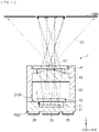
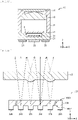
- FIG. 1 is a schematic cross-sectional view of an example of a schematic configuration of a lighting device (lighting device 1) according to an embodiment of the present the present disclosure.
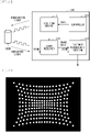
- FIG. 2 is a block diagram illustrating a schematic configuration of a distance measurement apparatus (distance measurement apparatus 100) including the lighting device 1 illustrated in FIG. 1 .
- the lighting device 1 according to the present embodiment shapes beam shapes of, out of light L1 and light L2 to be outputted from a light-emitting element 11 having multiple light-emitting sections (light-emitting sections 110 and 120, see FIG. 6 ), the light L2, for example, and performs spot irradiation as illustrated in FIG. 3 , uniform irradiation as illustrated in FIG. 4 , and the spot irradiation and the uniform irradiation simultaneously as illustrated in FIG. 5 , for example, on an irradiation target object 1000.
- the lighting device 1 includes, for example, the light-emitting element 11, a microlens array 12, a collimator lens 13, and a diffractive element 14.
- the microlens array 12, the collimator lens 13, and the diffractive element 14 are disposed on an optical path of the pieces of light (light L1 and light L2) outputted from the light-emitting element 11, for example, in this order.
- the light-emitting element 11 and the microlens array 12 are held, for example, by a holding section 21, and the collimator lens 13 and the diffractive element 14 are held, for example, by a holding section 22.
- the holding section 21 includes, for example, one cathode electrode 23 and two anode electrodes 24 and 25 on a surface 21S2 opposite to a surface 21S1 holding the light-emitting element 11 and the microlens array 12.
- each member included in the lighting device 1 will be described in detail.
- the light-emitting element 11 is, for example, a surface-emitting semiconductor laser including multiple light-emitting sections.
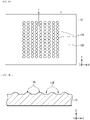
- the multiple light-emitting sections have a configuration in which, for example, multiple light-emitting sections to be used for spot irradiation (multiple light-emitting sections 110 for spot irradiation) and multiple light-emitting sections to be used for uniform irradiation (multiple light-emitting sections 120 for uniform irradiation) are disposed in an array on a substrate 130, for example.
- the multiple light-emitting sections 110 are electrically isolated from the multiple light-emitting sections 120.
- the multiple light-emitting sections 110 are electrically coupled to each other and the multiple light-emitting sections 120 are electrically coupled to each other.
- the multiple light-emitting sections 110 configure multiple (e.g., nine in FIG. 6 ) light-emitting section groups X (light-emitting section groups X1 to X9) including n-number of (e.g., 12 in FIG. 6 ) light-emitting sections 110 extending in one direction (e.g., a Y-axis direction).
- the multiple light-emitting sections 120 configure multiple (e.g., nine in FIG.
- light-emitting section groups Y (light-emitting section groups X1 to X9 including m-number of (e.g., nine in FIG. 6 ) light-emitting sections 120 extending in one direction (e.g., the Y-axis direction).
- the light-emitting section groups X1 to X9 and the light-emitting section groups Y1 to Y9 are alternately disposed on the substrate 130 having a rectangular shape.
- the light-emitting section groups X1 to X9 are electrically coupled to, for example, an electrode pad 240 provided along one side of the substrate 130.
- the light-emitting section groups Y1 to Y9 are electrically coupled to, for example, an electrode pad 250 provided along the other side opposed to the one side of the substrate 130.
- FIG. 6 illustrates the example in which the light-emitting section groups X1 to X9 and Y1 to Y9 are alternately disposed, the present disclosure is not limited thereto.
- the number of light-emitting sections 110 and light-emitting sections 120 may be any arrangement, depending on desired number, positions, and quantity of optical power, respectively, of light-emitting points.
- an array including the multiple light-emitting sections 120 may be disposed every two arrays each including the multiple light-emitting sections 110.
- FIG. 7 is an enlarged view of a portion of the arrangement of the multiple light-emitting sections 110 and the multiple light-emitting sections 120 illustrated in FIG. 6 .
- light-emission areas OA diameters W3 and W4
- the light-emission areas (OA diameters W3) of the multiple light-emitting sections 110 for spot irradiation be smaller than the light-emission areas (OA diameters W4) of the multiple light-emitting sections 120 for uniform irradiation.
- laser beams L110 see FIG.
- a width of an opening W1 of a wiring line that couples the multiple light-emitting sections 110 with each other is smaller than a width of an opening W2 of a wiring line that couples the multiple light-emitting sections 120 with each other.
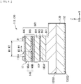
- FIG. 8 schematically illustrates an example of a cross-sectional configuration of the light-emitting section (light-emitting section 110, 120) of the light-emitting element 11.
- the light-emitting element 11 is a front side output type surface-emitting semiconductor laser.
- the light-emitting sections 110 and 120 each include a semiconductor layer 140 that includes, on one surface (front surface (surface 130S1)) side of the substrate 130, in the following order: a lower DBR layer 141; a lower spacer layer 142; an active layer 143; an upper spacer layer 144; an upper DBR layer 145; and a contact layer 146.
- An upper portion of the semiconductor layer 140 is in a form of a columnar mesa section 147.
- the substrate 130 is, for example, an n-type GaAs substrate.
- Examples of an n-type impurity include silicon (Si) and selenium (Se).
- the semiconductor layer 140 includes an AlGaAs-based compound semiconductor.
- the AlGaAs-based compound semiconductor represents a compound semiconductor including at least aluminum (Al) and gallium (Ga) out of group 3B elements in the short period periodic table, and at least arsenic (As) out of group 5B elements in the short period periodic table.
- the lower DBR layer 141 is configured by alternately stacking a low refractive index layer and a high refractive index layer (both not illustrated).
- the low refractive index layer includes, for example, n-type Al x-1 Ga 1-x1 As (0 ⁇ x1 ⁇ 1) having a thickness of ⁇ 0 /4 n1 ( ⁇ represents a light emission wavelength, n1 represents a refractive index).
- the high refractive index layer includes, for example, n-type Al x-2 Ga 1-x2 As (0 ⁇ x2 ⁇ x1) having a thickness of ⁇ 0 /4 n2 (n2 represents a refractive index).
- the lower spacer layer 142 includes, for example, n-type Al x-3 Ga 1-x3 As (0 ⁇ x3 ⁇ 1).
- the active layer 143 includes, for example, undoped n-type Al x-4 Ga 1-x4 As (0 ⁇ x4 ⁇ 1), for example.
- the upper spacer layer 144 includes, for example, p-type Al x-5 Ga 1-x5 As (0 ⁇ x5 ⁇ 1). Examples of a p-type impurity include zinc (Zn), magnesium (Mg), and beryllium (Be).
- the upper DBR layer 145 is configured by alternately stacking a low refractive index layer and a high refractive index layer (both not illustrated).
- the low refractive index layer includes, for example, p-type Al x6 Ga 1-x6 As (0 ⁇ x6 ⁇ 1) having a thickness of ⁇ 0 /4n 3 (n 3 represents a refractive index) (0 ⁇ x6 ⁇ 1).
- the high refractive index layer includes, for example, p-type Al x7 Ga 1-x7 As (0 ⁇ x7 ⁇ x6) having a thickness of ⁇ 0 /4n 4 (n 4 represents a refractive index).
- the contact layer 16 includes, for example, p-type Al x8 Ga 1-x8 As (0 ⁇ x8 ⁇ 1).
- the light-emitting element 11 is further provided with a current confining layer 148 and a buffer layer 149.
- the current confining layer 148 and the buffer layer 149 are provided within the upper DBR layer 145.
- the current confining layer 148 is formed at a position away from the active layer 143 in relation to the buffer layer 149.
- the current confining layer 148 is provided, for example, within the upper DBR layer 145, in a part of a low refractive index layer several layers away counting from a side of the active layer 143, for example, and is provided in place of the low refractive index layer.
- the current confining layer 148 has a current injection region 148A and a current confining region 148B.
- the current injection region 148A is formed in a middle region in a surface and corresponds the light-emission area (OA diameter W3, W4) of the light-emitting section 110, 120 described above.
- the current confining region 148B is formed on the periphery of the current injection region 148A, i.e., in an outer edge region of the current confining layer 148, and has a ring shape.
- the current injection region 148A includes, for example, p-type Al x9 Ga 1-x9 As (0.98 ⁇ x9 ⁇ 1).
- the current confining region 148B includes, for example, aluminum oxide (Al 2 O 3 ), and is obtained by oxidizing a layer to be oxidized (not illustrated) including, for example, p-type Al x9 Ga 1-x9 As, from a side surface of the mesa section 17.
- the current confining layer 148 has a function of confining electric current.
- the buffer layer 149 is formed closer to the active layer 143 in relation to the current confining layer 148.
- the buffer layer 149 is formed adjacently to the current confining layer 148. As illustrated in FIG. 8 , for example, the buffer layer 149 is formed in contact with a surface (lower surface) on a side of the active layer 143 of the current confining layer 148. It is to be noted that a thin layer having a thickness of, for example, about several nanometers may be provided between the current confining layer 148 and the buffer layer 149.
- the buffer layer 149 is provided, for example, within the upper DBR layer 145, in a part of a high refractive index layer which is several layers away from the current confining layer 148, for example, and is provided in place of the high refractive index layer.
- the buffer layer 149 has an unoxidized region and an oxidized region (both not illustrated).
- the unoxidized region is formed mainly in a center region of the surface, and is formed, for example, in a part in contact with the current injection region 148A.
- the oxidized region is formed on the periphery of the unoxidized region 19A and has a ring shape.
- the oxidized region is formed mainly in an outer edge region of the surface, and is formed, for example, in a part in contact with the current confining region 148B.
- the oxidized region is formed in a biased manner on a side of the current confining layer 148 in a portion other than a portion corresponding to the outer edge of the buffer layer 149.
- the unoxidized region includes a semiconductor material containing Al.
- the semiconductor material containing Al include p-type Al x10 Ga 1-x10 As (0.85 ⁇ x10 ⁇ 0.98) or p-type InAl x11 GaAs (0.85 ⁇ x11 ⁇ 0.98).
- the oxidized region includes, for example, an aluminum oxide (Al 2 O 3 ), and is obtained by oxidizing a layer to be oxidized (not illustrated) including, for example, p-type Al x10 Ga 1-x10 As or p-type InAl x11 GaAs, from a side of a side surface of the mesa section 147 and a side of the layer to be oxidized.
- the layer to be oxidized of the buffer layer 149 includes a material and has a thicknesses in such a manner as to have an oxidation rate which is higher than that of the lower DBR layer 141 and that of the upper DBR layer 145, and is lower than that of the layer to be oxidized of the current confining layer 148.
- An upper surface of the mesa section 147 (an upper surface of the contact layer 146) is provided with an upper electrode 151 having a ring shape.
- the upper electrode 151 has an opening (light exit window 151A) at least on a region opposed to the current injection region 148A. Further, an insulating layer (not illustrated) is formed on a front surface of the side surface and the periphery of the mesa section 147.
- the upper electrodes 151 are each coupled to the electrode pad 240 through a wiring line 111 illustrated in FIG. 7 .
- the upper electrodes 151 are each coupled to the electrode pad 250 through a wiring line 112 illustrated in FIG. 7 .
- the electrode pad 240 and the electrode pad 250 are coupled to respective electrodes provided on a front surface (the surface 21S1) of the holding section 21 to be described later by, for example, wire bonding, and are electrically coupled to the anode electrode 24 and the anode electrode 25, respectively, provided on a back surface (the surface 21S2) of the holding section 21.
- Another surface (back surface (surface 130S2) of the substrate 130 is provided with a lower electrode 152.
- the lower electrode 152 is electrically coupled to the cathode electrode 23 provided on, for example, the back surface (surface 21S2) of the holding section 21 to be described later.
- the cathode electrode is provided as a common electrode and the anode electrodes are provided individually; however, the anode electrodes may be provided as common electrodes and the cathode electrode may be provided individually, depending on a structure of the light-emitting element 11.
- the upper electrode 151, the electrode pads, and the coupling sections are configured by stacking, for example, titanium (Ti), platinum (Pt), and gold (Au) in this order, and are electrically coupled to the contact layer 146 on an upper portion of the mesa section 147.
- the lower electrode 152 has a structure in which, for example, an alloy of gold (Au) and germanium (Ge), nickel (Ni), and gold (Au) are stacked in this order from a side of the substrate 130, and is electrically connected to the substrate 130.
- the microlens array 12 shapes beam shapes of the pieces of light (laser beams L110) to be outputted from the multiple light-emitting sections 110 for spot irradiation, beam shapes of the pieces of light (laser beams L120) to be outputted from the multiple light-emitting sections 120, or both the beam shapes of the laser beams L110 and the beam shapes of the laser beams L120, and outputs the laser beams L110 and the laser beams L120, for example.
- the microlens array 12 corresponds to a specific example of a "second optical member" according to the present disclosure.
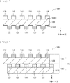
- FIG. 9A schematically illustrates an example of a plane configuration of the microlens array 12, and FIG.
- the microlens array 12 includes multiple microlenses disposed in an array, and has multiple lens sections 12A and a parallel flat plate section 12B.
- the lens sections 12A are disposed in such a manner as to be directly opposed to the multiple light-emitting sections 120 for uniform irradiation as illustrated in FIG. 10A
- the parallel flat plate section 12B is disposed in such a manner as to be directly opposed to the multiple light-emitting sections 110 for spot irradiation as illustrated in FIG. 10B .
- the laser beams L120 outputted from the multiple light-emitting sections 120 are refracted by lens surfaces of the lens sections 12A to provide a virtual light-emitting point P2' in the microlens array 12, for example.
- a light-emitting point P2 of the multiple light-emitting sections 120 located at the same height as a light-emitting point P1 of the multiple light-emitting sections 110 is shifted in an optical axis direction (for example, a Z-axis direction) of the light (laser beams L110 and laser beams L120) to be outputted from the multiple light-emitting sections 110 and the multiple light-emitting sections 120.
- an optical axis direction for example, a Z-axis direction
- the laser beams L110 outputted from the multiple light-emitting sections 110 form a spot-shaped irradiation pattern as illustrated in FIG. 3 or FIG. 12 , for example; and the laser beams L120 outputted from the multiple light-emitting sections 120 form an irradiation pattern irradiated with light of a substantially uniform light intensity over a predetermined range, by overlapping portions of the laser beams L120 outputted from adjacent light-emitting sections 120 with each other as illustrated in FIG. 4 or FIG. 12 , for example.
- the lighting device 1 is able to perform switching between the spot irradiation and the uniform irradiation, by performing switching of light emission between the multiple light-emitting sections 110 and the multiple light-emitting sections 120.
- FIG. 11 illustrates an example in which the microlens array 12 functions as a relay lens; however, the present disclosure is not limited thereto.
- the virtual light-emitting point P2' of the multiple light-emitting sections 120 may be provided between the light-emitting section 120 and the microlens array 12.
- the collimator lens 13 outputs the laser beams L110 outputted from the multiple light-emitting sections 110 and the laser beams L120 outputted from the multiple light-emitting sections 120 as substantially collimated light.
- the collimator lens 13 corresponds to a specific example of a "first optical member" according to the present disclosure.
- the collimator lens 13 is, for example, a lens for collimating the laser beams L110 and the laser beams L120 outputted from the microlens array 12, and combining the laser beams L110 and the laser beams L120 with the diffractive element 14.
- the diffractive element 14 divides and outputs each of the laser beams L110 outputted from the multiple light-emitting sections 110 and the laser beams L120 outputted from the multiple light-emitting sections 120. It is possible to use a diffractive optical element (DOE) as the diffractive element 14, for example.
- DOE diffractive optical element
- the diffractive optical element divides each of the laser beams L110 outputted from the multiple light-emitting sections 110 and the laser beams L120 outputted from the multiple light-emitting sections 120 into 3 ⁇ 3.
- Luminous fluxes of the laser beams L110 and the laser beams L120 are tiled by disposing the diffractive element 14, and this makes it possible to increase the number of spots based on a timing at which the spot irradiation is performed and to increase the irradiation range based on a timing at which the uniform irradiation is performed, for example.
- the holding section 21 and the holding section 22 are for holding the light-emitting element 11, the microlens array 12, the collimator lens 13, and the diffractive element 14.
- the holding section 21 holds the light-emitting element 11 in a concave section C provided in an upper surface (the surface 21S1) and holds the microlens array 12 along the surface 21S1.
- the holding section 22 holds the collimator lens 13 and the diffractive element 14.
- the microlens array 12 is held by the holding section 21 with an adhesive, for example, and the collimator lens 13 and the diffractive element 14 are each held by the holding section 22 with an adhesive, for example.
- the holding section 21 and the holding section 22 are coupled to each other in such a manner as to cause the light L1 (specifically, the laser beam L110) and the light L2 (specifically, the laser beam L120) outputted from the light-emitting element 11 to enter predetermined positions of the microlens array 12, and to cause the light L1 and the light L2 transmitted through the collimator lens 13 to be substantially collimated.
- the light L1 specifically, the laser beam L110
- the light L2 specifically, the laser beam L120
- the surface 21S2 of the holding section 21 is provided with: the cathode electrode 23 shared by the multiple light-emitting sections 110 for spot irradiation and the multiple light-emitting sections 120 for uniform irradiation; the anode electrode 24 for the multiple light-emitting sections 110 for spot irradiation; and the anode electrode 25 for the multiple light-emitting sections 120 for uniform irradiation.
- a cathode electrode for the multiple light-emitting sections 110 for spot irradiation and a cathode electrode for the multiple light-emitting sections 120 for uniform irradiation may be provided individually, or an anode electrode may be provided as a common electrode for the multiple light-emitting sections 110 for spot irradiation and the multiple light-emitting sections 120 for uniform irradiation. Further, FIG.
- the present disclosure is not limited thereto, and the microlens array 12 may be held by the holding section 22, for example.
- the collimator lens 13 and the diffractive element 14 may be held by the holding section 21.
- the light-emitting section group X including the multiple light-emitting sections 110 for spot irradiation and the light-emitting section group Y including the multiple light-emitting sections 120 for uniform irradiation provided on the light-emitting element 11 are driven independently of each other.
- the lighting device 1 is able to perform the spot irradiation and the uniform irradiation in one device, by performing switching of light emission between the light-emitting section group X and light-emitting section group Y.
- the spot irradiation is to irradiate the irradiation target object 1000 with mutually independent spot-shaped light beams (laser beams L110).
- the uniform irradiation is to irradiate a predetermined range with light beams of a substantially uniform light intensity (laser beams L120).
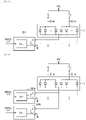
- FIG. 13 illustrates an example of a configuration of a drive circuit of the lighting device 1.
- the switching between the light-emitting section group X and the light-emitting section group X2 is able to be achieved by, for example, an external switching switch using one driver 260.
- the switching between the light-emitting section group X and the light-emitting section group X2 is also able be performed using two drivers 260A and 240B, for example, as illustrated in FIG. 14 .
- the switching between the light-emitting section group X and the light-emitting section group X2 by using two drivers 260A and 240B makes it possible to individually control driving conditions including electric currents, voltages, and the like of the light-emitting section group X that performs the spot irradiation and the light-emitting section group Y that performs the uniform irradiation.
- the driver 260 may be provided outside the lighting device 1, for example, or may be built in the holding section 21, for example. Further, the light-emitting element 11 and the driver 260 may be directly coupled to each other.
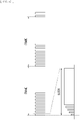
- FIG. 15 illustrates a light-emission sequence of the lighting device 1.
- the switching of light emission between the light-emitting section group X and the light-emitting section group Y may be performed, for example, on a per-frame basis or on a per-block basis.
- the switching of light emission between the light-emitting section group X and the light-emitting section group Y may be performed in units of multiple blocks. This makes it possible to perform switching between the spot irradiation and the uniform irradiation at a high speed as compared with, for example, a system in which a focal position of laser beams outputted from the multiple light-emitting sections is mechanically switched.
- the distance measurement apparatus 100 illustrated in FIG. 2 measures a distance by the ToF method.
- the distance measurement apparatus 100 includes, for example, the lighting device 1, a light receiver 210, a controller 220, and a distance measurement section 230.
- the lighting device 1 irradiates the irradiation target object 1000 with spot-shaped light beams (spot irradiation) and with light beams of a substantially uniform light intensity (uniform irradiation), by performing switching of light emission between the multiple light-emitting sections 110 and the multiple light-emitting sections 120.
- the lighting device 1 generates, for example, irradiation light in synchronization with a light-emission control signal CLKp of a rectangular wave.
- the light-emission control signal CLKp is not limited to the rectangular wave as long as it is a periodic signal.
- the light-emission control signal CLKp may be a sine wave.
- the light receiver 210 receives light reflected from the irradiation target object 1000, and detects, every time a period of a vertical synchronization signal VSYNC elapses, a received light amount within the period.
- a periodic signal of 60 hertz (Hz) is used as the vertical synchronization signal VSYNC.
- multiple pixel circuits are disposed in a two-dimensional lattice shape.
- the light receiver 210 supplies image data (a frame) corresponding to the received light amount of the pixel circuits to the distance measurement section 230.
- a frequency of the vertical synchronization signal VSYNC is not limited to 60 hertz (Hz), may be 30 hertz (Hz) or 120 hertz (Hz).
- the controller 220 controls the lighting device 1.
- the controller 220 generates the light-emission control signal CLKp and supplies the lighting device 1 and the light receiver 210 with the light-emission control signal CLKp.
- a frequency of the light-emission control signal CLKp is, for example, 20 megahertz (MHz). It is to be noted that the frequency of the light-emission control signal CLKp is not limited to 20 megahertz (MHz), and may be 5 megahertz (MHz), for example.
- the distance measurement section 230 measures a distance to the irradiation target object 1000 by the ToF method on the basis of the image data.
- the distance measurement section 230 measures a distance for each pixel circuit and generates a depth map which indicates a distance to an object for each pixel by a gradation value.
- This depth map is used, for example, for image processing in which blurring processing with a degree corresponding to a distance is performed, auto focus (AF) processing in which a focused focal point of a focus lens is determined according to a distance, or the like.
- the microlens array 12 is disposed on the optical path of the light L1 (laser beams L110) and the light L2 (laser beams L120).
- the microlens array 12 shapes, for example, the beam shapes of the laser beams L120 for uniform irradiation and outputs the laser beams.
- the laser beams L110 and the laser beams L120 are to be outputted from the light-emitting element 11 including the multiple light-emitting sections (the multiple light-emitting sections 110 and the multiple light-emitting sections 120) that configures the light-emitting section groups X for spot irradiation and the light-emitting section groups Y for uniform irradiation.
- the distance measurement apparatus that uses the ToF method performs: a method of uniformly applying pieces of light outputted from the multiple light-emitting sections on an entire surface of a measurement target range; and a method of causing pieces of light outputted from the multiple light-emitting sections to be substantially collimated by the collimator lens, and applying the pieces of spot-shaped light outputted on the entire surface of the measurement target range.
- a distance measurement apparatus including two light sources i.e., a light source for uniform irradiation and a light source for spot irradiation
- a distance measurement apparatus including two light sources i.e., the light source for uniform irradiation and the light source for spot irradiation
- the distance measurement apparatus including two light sources is able to compensate reduction in XY resolution by the uniform irradiation while increasing a distance measurement distance by increasing light density by the spot irradiation.
- the use of two light sources having differing irradiation patterns is an effective technique for increasing the distance measurement accuracy; however, there are issues that cost may increase and a size of the apparatus may increase due to the use of two light sources. In addition, there are also issues that adjustment of relative positions of the two light sources may be necessary in manufacturing the distance measurement apparatus, and positional deviation may occur due to temporal change.
- the microlens array 12 is disposed on the optical path of the laser beams L110 and the laser beams L120 to be outputted from the light-emitting element 11 including the multiple light-emitting sections 110 for spot irradiation and the multiple light-emitting sections 120 for uniform irradiation.
- the microlens array 12 has the lens sections 12A and the parallel flat plate section 12B, and is disposed, for example, in such a manner that the laser beams L110 outputted from the multiple light-emitting sections 110 enter the parallel flat plate section 12B and the laser beams L120 outputted from the multiple light-emitting sections 120 enter the lens sections 12A.
- the laser beams L120 that have entered the lens section 12A are refracted by the lens surface of the lens section 12A to change the beam shape, and the virtual light-emitting point P2' is provided in microlens array 12, for example.
- the lighting device 1 makes it possible to perform the spot irradiation and the uniform irradiation on the irradiation target object 1000 without using, for example, an adjusting mechanism that mechanically adjusts a position of an optical member (e.g., the collimator lens 13) disposed in an outputting direction of the multiple light-emitting sections 110 for spot irradiation and the multiple light-emitting sections 120 for uniform irradiation in accordance with each irradiation mode. Therefore, it is possible to achieve downsizing of the lighting device 1 and the distance measurement apparatus 100 including the same.
- an optical member e.g., the collimator lens 13
- the present embodiment does not necessitate the above-described adjusting mechanism; thus, it is possible to reduce cost. Still further, positional deviation or the like of the optical member due to temporal change does not occur; thus, it is possible to improve reliability. Moreover, in the present embodiment, it is possible to switch the irradiation modes at a high speed, which makes it possible to accurately measure a distance of a moving object.
- the present embodiment uses the surface-emitting semiconductor laser including the multiple light-emitting sections is used as a light source, and some of the light-emitting sections are used as the multiple light-emitting sections 110 for spot irradiation, and the remaining light-emitting sections are used as the multiple light-emitting sections 120 for uniform irradiation.
- the light-emission areas (OA diameters W3 and W4) of the multiple light-emitting sections 110 for spot irradiation and the multiple light-emitting sections 120 for uniform irradiation are set in such a manner that the OA diameters W3 of the multiple light-emitting sections 110 for spot irradiation are relatively small and the OA diameters W4 of the multiple light-emitting sections 120 for uniform irradiation are relatively large.
- FIG. 16 illustrates a beam shaping function of the microlens array 12 according to a modification example 1 of the present disclosure.
- the embodiment described above illustrates the example in which the lens sections 12A are disposed in such a manner as to be directly opposed to the multiple light-emitting sections 120 for uniform irradiation and the parallel flat plate section 12B is disposed in such a manner as to be directly opposed to the multiple light-emitting sections 110 for spot irradiation; however, the present disclosure is not limited thereto.
- the lens sections 12A may be disposed in such a manner as to be directly opposed to the multiple light-emitting sections 110 for spot irradiation and the parallel flat plate section 12B may be disposed in such a manner as to be directly opposed to the multiple light-emitting sections 120 for uniform irradiation. Also with such a configuration, it is possible to obtain similar effects as in the above-described embodiment.
- FIG. 17A schematically illustrates an example of a plane configuration of the microlens array 12 according to a modification example 2 of the present disclosure
- FIG. 17B schematically illustrates a cross-sectional configuration of the microlens array 12 taken along a line II-II illustrated in FIG. 17A
- the microlens array 12 illustrated in FIG. 17A and FIG. 17B has two types of microlenses whose curvature radii are different from each other disposed in an array.
- the microlens array 12 includes multiple lens sections 12A and multiple lens sections 12C, and the curvature radii are different between the multiple lens sections 12A and the multiple lens sections 12C.
- the configuration is described in which the laser beams L110 outputted from the multiple light-emitting sections 110 or the laser beams L120 outputted from the multiple light-emitting sections 120 enter the lens sections 12A and the other of the laser beams L110 and the laser beams L120 enter the parallel flat plate section 12B; however, the present disclosure is not limited thereto.
- the multiple light-emitting sections 120 for uniform irradiation may be disposed in such a manner as to be directly opposed to the lens sections 12A and the multiple light-emitting sections 110 for spot irradiation may be disposed in such a manner as to be directly opposed to the lens sections 12C.
- the laser beams L110 and laser beams L120 outputted from the multiple light-emitting sections 110 and the multiple light-emitting sections 120 may enter the lens sections 12C and the lens sections 12A, respectively.
- the laser beams L120 outputted from the multiple light-emitting sections 120 are refracted by lens surfaces of the lens sections 12A to provide the virtual light-emitting point P2' in the microlens array 12, for example.
- the laser beams L110 outputted from the multiple light-emitting sections 110 are refracted by lens surfaces of the lens sections 12C to provide a virtual light-emitting point P1' behind the multiple light-emitting sections 110, for example.
- the present modification example uses the microlens array 12 having two types of lens sections (the lens sections 12A and the lens sections 12C) whose curvature radii are different from each other, and causes the laser beams L110 to be outputted from the multiple light-emitting sections 110 for spot irradiation and the laser beams L120 to be outputted from the multiple light-emitting sections 120 for uniform irradiation to enter the lens sections, thereby shaping beam shapes of both the laser beams L110 and the laser beams L120.
- FIG. 19 is a schematic cross-sectional view of an example of a schematic configuration of a lighting device (lighting device 1A) according to a modification example 3 of the present disclosure.
- the lighting device 1A according to the present modification example differs from the above-described embodiment in that a diffractive optical element (DOE) 32 is used as the second optical member.
- DOE diffractive optical element
- the diffractive optical element 32 shapes beam shapes of the pieces of light (laser beams L110) to be outputted from the multiple light-emitting sections 110 for spot irradiation, beam shapes of the pieces of light (laser beams L120) to be outputted from the multiple light-emitting sections 120, or both the beam shapes of the laser beams L110 and the beam shapes of the laser beams L120, and outputs the laser beams L110 and the laser beams L120, for example.
- FIG. 20 schematically illustrates an example of a plane configuration of the diffractive optical element 32, in which, for example, the multiple light-emitting sections 120 for uniform irradiation are disposed in such a manner as to be directly opposed to regions 32A and the multiple light-emitting sections 110 for spot irradiation are disposed in such a manner as to be directly opposed to regions 32B.
- the diffractive optical element 32 for example, a Fresnel lens having a plane pattern as illustrated in FIG. 21 and a cross-sectional pattern as illustrated in FIG. 22 may be used in the region 32A. It is to be noted that the region 32B is, for example, a parallel-plate region.
- the laser beams L120 outputted from the multiple light-emitting sections 120 may form, for example, an irradiation pattern as illustrated in FIG. 23 on the irradiation target object 1000.
- the diffractive optical element 32 for example, a binary lens having a cross-sectional pattern as illustrated in FIG. 24 may be used in the region 32A.
- the laser beams L120 outputted from the multiple light-emitting sections 120 may form, for example, an irradiation pattern as illustrated in FIG. 25 by pieces of +1st order light and pieces of -1st order light being overlapped with each other.
- the diffractive optical element 32 for example, a DOE corresponding to a saddle lens having a plane pattern as illustrated in FIG. 26A may be used in the region 32A.
- the plane patterns illustrated in FIG. 26A are disposed in such a manner as to be rotated by 45° in an adjacent region, as illustrated in FIG. 26B .
- the laser beams L120 outputted from the multiple light-emitting sections 120 form an irradiation pattern as illustrated in FIG. 27 , for example. This makes it possible to improve reduction in uniformity with respect to deviation in the optical axis direction.
- the diffractive optical element 32 such as the Fresnel lens is used as the second optical member of the present disclosure.
- the diffractive optical element 32 such as the Fresnel lens is used as the second optical member of the present disclosure.
- a diffuser may be used as the second optical member according to the present disclosure.
- expected positional accuracy is relaxed and it is possible to reduce the cost, as compared with the case of using the microlens array 12 or the diffractive optical element 32.
- FIG. 28 is a schematic cross-sectional view of an example of a schematic configuration of a lighting device (lighting device 1B) according to a modification example 4 of the present disclosure.
- the lighting device 1B according to the present modification example differs from the above-described embodiment in that the diffractive element 14 and a diffractive element 34 are disposed in the optical path of the laser beams L110 and the laser beams L120 outputted from the multiple light-emitting sections 110 and the multiple light-emitting sections 120, respectively, for example, in a subsequent stage of the collimator lens 13.
- the diffractive element 34 divides and outputs the laser beams L110 outputted from the multiple light-emitting sections 110 and the laser beams L120 outputted from the multiple light-emitting sections 120.
- the diffractive element 34 is, for example, a simple diffraction grating in which a number of parallel slits are provided at equal intervals.
- the diffractive element 34 corresponds to a specific example of a "third optical member" according to the present disclosure.
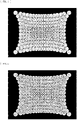
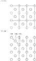
- FIG. 29A illustrates an irradiation pattern of the laser beams L110 for spot irradiation outputted from the multiple light-emitting sections 110 on the irradiation target object 1000, in a case where the diffractive element 34 is not disposed.
- FIG. 29A further illustrates an irradiation pattern of the laser beams L120 whose beam shapes are unprocessed, where the irradiation pattern of the laser beams L110 is represented by a solid line and the irradiation pattern of the laser beams L120 is represented by a dotted line.
- FIG. 29B illustrates an irradiation pattern of the laser beams L110 outputted from the multiple light-emitting sections 110 to be applied on the irradiation target object 1000, in a case where the diffractive element 34 is disposed.
- disposing the diffractive element 34 causes the spot irradiation to be performed in such a manner that: pieces of 0th order light (110X 0 ) out of the laser beams L110 transmitted through the diffractive element 34 are applied on irradiation positions of the laser beams L110 of the case where the diffractive element 34 is not disposed; and pieces of +1st order light (110X +1 ) and pieces of -1st order light (110X -1 ) are applied on irradiation positions of the laser beams L120 whose beam shapes are unprocessed, for example.
- disposing the diffractive element 34 makes it possible to further increase the number of light spots to be applied on the irradiation target object 1000.
- the laser beams L120 for uniform irradiation to be outputted from the multiple light-emitting sections 120 are also diffracted in the similar manner as the laser beams L110 for spot irradiation, which makes it possible to further improve the uniformity of the light intensity based on the timing at which the uniform irradiation is performed owing to the overlapping of the pieces of diffracted light.
- the diffractive element 34 is further disposed on the optical path of the laser beams L1110 and the laser beams L120 outputted from the multiple light-emitting sections 110 and the multiple light-emitting sections 120, respectively.
- This makes it possible to perform the spot irradiation and the uniform irradiation with high optical density on the irradiation target object 1000, as compared with the above-described embodiment and the like.
- the spot irradiation enables measurement of a distance to a farther object with high accuracy.
- the uniform irradiation enables measurement of a distance to a closer object with higher resolution.
- the present modification example illustrates the example in which the diffraction element 14 and the diffractive element 34 are configured as separate components; however, a diffractive optical surface may be provided on each of both sides of one optical element.
- FIG. 28 illustrates the example in which the diffractive element 34 is disposed in the subsequent stage of the collimator lens 13; however, the position at which the diffractive element 34 is disposed not limited thereto, and may be disposed between the microlens array 12 and the collimator lens 13, for example.
- the present modification example illustrates the example in which the simple diffraction grating is used as the diffractive element 34: however, a diffractive optical element (DOE) having a more complicated diffraction pattern may be used, for example.
- the diffractive element 34 may be integrated with the microlens array 12, for example. In this case, effects may be applied only to the laser beams L110 for spot irradiation or only to the laser beams L120 for uniform irradiation, for example. Further, the laser beams L110 for spot irradiation and the laser beams L120 for uniform irradiation may form diffraction patterns that are different from each other.
- FIG. 30 is a schematic cross-sectional view of an example of a schematic configuration of a lighting device (lighting device 1C) according to a modification example 5 of the present disclosure.
- the lighting device 1C according to the present modification example differs from the above-described embodiment in that a back side output type surface-emitting semiconductor laser is used as a light-emitting element 31.
- FIG. 31 illustrates an example of a cross-sectional configuration of the light-emitting element 31 in the lighting device 1C and a positional relationship with the microlens array 12.
- the light-emitting element 31 is the back side output type surface-emitting semiconductor laser, and has multiple light-emitting sections 310 and 320 for spot irradiation and uniform irradiation formed in an array on the back surface (surface 130S2) side of the substrate 130.
- the surface 130S2 of the substrate 130 is further provided with an electrode pad 340 for applying voltage to the multiple light-emitting sections 310 and an electrode pad 350 for applying voltage to the multiple light-emitting sections 320. Except for those points, the light-emitting element 31 has a similar configuration as the light-emitting element 11 described above.
- the back side irradiation type surface-emitting semiconductor laser may be used in the lighting device according to the present disclosure.
- the back side irradiation type surface-emitting semiconductor laser as the light-emitting element 31 makes it possible to reduce regions of the multiple electrode pads. Further, it is possible to perform the switching between the spot irradiation and the uniform irradiation easily, as compared with the above-described embodiment.
- the second optical member and the light-emitting element 31 in an integrated manner.
- microlenses 42 are disposed at positions directly opposed to the multiple light-emitting sections 320 for uniform irradiation, for example, on the front surface (surface 130S1) of the substrate 130 of the light-emitting element 31. This makes it possible to dispose the second optical member with higher positional accuracy. Further, it is possible to reduce the cost as compared with a case where the optical member such as a microlens array 12 is separately disposed.
- FIG. 32 illustrates the example in which the microlens 42 is disposed as the second optical member; however, the present disclosure is not limited thereto, and a diffractive optical element such as the Fresnel lens, or a diffuser may be disposed.
- FIG. 33 schematically illustrates another example of a cross-sectional configuration of the light-emitting element 11 according to a modification example 6 of the present disclosure.
- the example in which the light-emitting element 11 having the multiple light-emitting sections 110 for spot irradiation and the multiple light-emitting sections 120 for uniform irradiation on the same plane is used.
- the multiple light-emitting sections 110 and the multiple light-emitting sections 120 may be formed on different planes.
- the multiple light-emitting sections 110 and the multiple light-emitting sections 120 may be provided on the front surface (surface 130S1) of the substrate 130, in such a manner that the multiple light-emitting sections 110 are different from the multiple light-emitting sections 120 in height.
- the height is determined with respect to the optical axis direction (for example, the Z-axis direction) of the laser beams L110 and the laser beams L120 to be outputted from the multiple light-emitting sections 110 and the multiple light-emitting sections 120, respectively.
- the multiple light-emitting sections 110 or the multiple light-emitting sections 120 may be provided on the front surface (surface 130S1) side of the substrate 130, and the other (for example, the multiple light-emitting sections 120) may be provided on the back surface (surface 130S2) side of the substrate 130.
- the multiple light-emitting sections of one type may use the front side output type surface-emitting semiconductor laser, and the multiple light-emitting sections of the other type may use the back side output type surface-emitting semiconductor laser.
- a light-emitting element 11Ca having the multiple light-emitting sections 110 for spot irradiation and a light-emitting element 11Cb having the multiple light-emitting sections 120 for uniform irradiation may be provided, and may be used by stacking them.
- providing steps in the light-emitting element 11 between the multiple light-emitting sections 110 for spot irradiation and the multiple light-emitting sections 120 for uniform irradiation makes it possible to further improve the uniformity of the light intensity at the timing at which the uniform irradiation is performed, without separately disposing the diffractive element 34 as in the above-described modification example 4, for example.
- FIG. 21 and FIG. 26 illustrate the DOE (diffractive optical element 32) having a period greater than the wavelength; however, a structure smaller than the wavelength may be provided with a beam shaping function using a so-called metamaterial.
- a second optical member is disposed which: shapes beam shapes of, out of pieces of light (multiple pieces of first light and multiple pieces of second light) to be outputted from a light-emitting element having multiple first light-emitting sections and multiple second light-emitting sections, the multiple pieces of first light, the multiple pieces of second light, or both; and outputs the pieces of light.
- a light-emitting element having multiple first light-emitting sections and multiple second light-emitting sections, the multiple pieces of first light, the multiple pieces of second light, or both
- outputs the pieces of light This makes it possible to change positions of light-emitting points of the multiple pieces of first light and the multiple pieces of second light. Therefore, it is possible to achieve downsizing of a lighting device and a distance measurement apparatus including the same.
Landscapes
- Physics & Mathematics (AREA)
- Engineering & Computer Science (AREA)
- General Physics & Mathematics (AREA)
- Remote Sensing (AREA)
- Computer Networks & Wireless Communication (AREA)
- Radar, Positioning & Navigation (AREA)
- Optics & Photonics (AREA)
- Electromagnetism (AREA)
- General Engineering & Computer Science (AREA)
- Semiconductor Lasers (AREA)
- Non-Portable Lighting Devices Or Systems Thereof (AREA)
- Microelectronics & Electronic Packaging (AREA)
- Measurement Of Optical Distance (AREA)
Applications Claiming Priority (2)
| Application Number | Priority Date | Filing Date | Title |
|---|---|---|---|
| JP2019188724 | 2019-10-15 | ||
| PCT/JP2020/038090 WO2021075340A1 (ja) | 2019-10-15 | 2020-10-08 | 照明装置および測距装置 |
Publications (2)
| Publication Number | Publication Date |
|---|---|
| EP4024629A1 true EP4024629A1 (de) | 2022-07-06 |
| EP4024629A4 EP4024629A4 (de) | 2022-10-12 |
Family
ID=75537963
Family Applications (1)
| Application Number | Title | Priority Date | Filing Date |
|---|---|---|---|
| EP20876299.7A Pending EP4024629A4 (de) | 2019-10-15 | 2020-10-08 | Beleuchtungsvorrichtung und ranging-vorrichtung |
Country Status (4)
| Country | Link |
|---|---|
| US (1) | US12566266B2 (de) |
| EP (1) | EP4024629A4 (de) |
| JP (1) | JPWO2021075340A1 (de) |
| WO (1) | WO2021075340A1 (de) |
Cited By (1)
| Publication number | Priority date | Publication date | Assignee | Title |
|---|---|---|---|---|
| US20240113496A1 (en) * | 2022-09-29 | 2024-04-04 | Zebra Technologies Corporation | Compact Optical System For A VCSEL Based Laser Aim Pattern Generator |
Families Citing this family (6)
| Publication number | Priority date | Publication date | Assignee | Title |
|---|---|---|---|---|
| WO2022176389A1 (ja) * | 2021-02-16 | 2022-08-25 | ソニーセミコンダクタソリューションズ株式会社 | 光学モジュールおよび距離測定装置 |
| WO2022209375A1 (ja) * | 2021-03-31 | 2022-10-06 | ソニーセミコンダクタソリューションズ株式会社 | 発光素子、照明装置、および、測距装置 |
| US12163634B2 (en) * | 2021-10-08 | 2024-12-10 | Ii-Vi Delaware, Inc. | Shared optic assembly for combined dot and flood illumination modules |
| WO2024013948A1 (ja) * | 2022-07-14 | 2024-01-18 | 日清紡マイクロデバイス株式会社 | 半導体レーザ駆動装置 |
| JP2024011627A (ja) * | 2022-07-15 | 2024-01-25 | キヤノン株式会社 | 光学装置、車載システム、および移動装置 |
| JP2024081358A (ja) * | 2022-12-06 | 2024-06-18 | ソニーセミコンダクタソリューションズ株式会社 | 照明装置及び測距装置 |
Family Cites Families (22)
| Publication number | Priority date | Publication date | Assignee | Title |
|---|---|---|---|---|
| JP4985100B2 (ja) * | 2007-05-28 | 2012-07-25 | ソニー株式会社 | 多波長レーザ、光ピックアップ装置および光ディスク装置 |
| EP2235584B1 (de) * | 2008-01-21 | 2020-09-16 | Apple Inc. | Optische entwürfe für eine reduktion nullter ordnung |
| US8995493B2 (en) | 2009-02-17 | 2015-03-31 | Trilumina Corp. | Microlenses for multibeam arrays of optoelectronic devices for high frequency operation |
| DE102011107893A1 (de) * | 2011-07-18 | 2013-01-24 | Heraeus Noblelight Gmbh | Optoelektronisches Modul mit verbesserter Optik |
| JP6339665B2 (ja) | 2013-04-22 | 2018-06-06 | トリルミナ コーポレーション | 高周波動作のための光電子装置のマルチビームアレイ用マイクロレンズ |
| CN113745962A (zh) | 2013-06-19 | 2021-12-03 | 苹果公司 | 集成结构化光投影仪 |
| EP3259612B1 (de) * | 2015-02-19 | 2018-09-26 | Koninklijke Philips N.V. | Infrarotlaserbeleuchtungsvorrichtung |
| JP2017102319A (ja) * | 2015-12-03 | 2017-06-08 | 日立金属株式会社 | 光モジュール及びその製造方法 |
| WO2018191489A1 (en) * | 2017-04-12 | 2018-10-18 | Sense Photonics, Inc. | Ultra-small vertical cavity surface emitting laser (vcsel) and arrays incorporating the same |
| CN107424188B (zh) * | 2017-05-19 | 2020-06-30 | 深圳奥比中光科技有限公司 | 基于vcsel阵列光源的结构光投影模组 |
| US10705214B2 (en) | 2017-07-14 | 2020-07-07 | Microsoft Technology Licensing, Llc | Optical projector having switchable light emission patterns |
| US10514444B2 (en) * | 2017-07-28 | 2019-12-24 | OPSYS Tech Ltd. | VCSEL array LIDAR transmitter with small angular divergence |
| EP3447862A1 (de) * | 2017-08-23 | 2019-02-27 | Koninklijke Philips N.V. | Vcsel-array mit integrierter optischer vorrichtung auf gemeinsamer waferebene |
| US10355456B2 (en) * | 2017-09-26 | 2019-07-16 | Lumentum Operations Llc | Emitter array with variable spacing between adjacent emitters |
| US11126060B2 (en) * | 2017-10-02 | 2021-09-21 | Liqxtal Technology Inc. | Tunable light projector |
| US11662433B2 (en) * | 2017-12-22 | 2023-05-30 | Denso Corporation | Distance measuring apparatus, recognizing apparatus, and distance measuring method |
| JP7238343B2 (ja) * | 2017-12-22 | 2023-03-14 | 株式会社デンソー | 距離測定装置及び距離測定方法 |
| CN108169981A (zh) | 2018-01-15 | 2018-06-15 | 深圳奥比中光科技有限公司 | 多功能照明模组 |
| JP6870650B2 (ja) | 2018-04-26 | 2021-05-12 | 京セラドキュメントソリューションズ株式会社 | 画像形成装置、報知方法 |
| CN108828563B (zh) * | 2018-06-08 | 2021-03-05 | 上海禾赛科技股份有限公司 | 一种激光发射装置 |
| CN113253474A (zh) * | 2019-01-25 | 2021-08-13 | 深圳市光鉴科技有限公司 | 可切换式漫射器投射系统和方法 |
| CN110412544A (zh) * | 2019-08-23 | 2019-11-05 | 上海禾赛光电科技有限公司 | 激光发射系统以及包括所述激光发射系统的激光雷达 |
-
2020
- 2020-10-08 JP JP2021552354A patent/JPWO2021075340A1/ja active Pending
- 2020-10-08 EP EP20876299.7A patent/EP4024629A4/de active Pending
- 2020-10-08 WO PCT/JP2020/038090 patent/WO2021075340A1/ja not_active Ceased
- 2020-10-08 US US17/760,882 patent/US12566266B2/en active Active
Cited By (1)
| Publication number | Priority date | Publication date | Assignee | Title |
|---|---|---|---|---|
| US20240113496A1 (en) * | 2022-09-29 | 2024-04-04 | Zebra Technologies Corporation | Compact Optical System For A VCSEL Based Laser Aim Pattern Generator |
Also Published As
| Publication number | Publication date |
|---|---|
| US12566266B2 (en) | 2026-03-03 |
| EP4024629A4 (de) | 2022-10-12 |
| US20220342070A1 (en) | 2022-10-27 |
| WO2021075340A1 (ja) | 2021-04-22 |
| JPWO2021075340A1 (de) | 2021-04-22 |
Similar Documents
| Publication | Publication Date | Title |
|---|---|---|
| US12566266B2 (en) | Lighting device and distance measurement apparatus | |
| US20240019547A1 (en) | Illumination apparatus and ranging apparatus | |
| JP7550221B2 (ja) | 光学モジュールおよび距離測定装置 | |
| US20230194671A1 (en) | Light emitting device and distance measuring device | |
| US20240069162A1 (en) | Solid-state lidar and method for detection using same | |
| CN113589322A (zh) | 一种面向多线激光雷达的vcsel线性阵列 | |
| EP3690494B1 (de) | Linsenarray und optisches beleuchtungssystem | |
| JP2022500880A (ja) | 位相結合されたレーザ装置、および位相結合されたレーザ装置を製造するための方法 | |
| CN115201844A (zh) | 固态激光雷达及使用其进行探测的方法 | |
| US20240310489A1 (en) | Illumination device and distance measuring device | |
| KR102915218B1 (ko) | 표면발광 레이저소자, 카메라 모듈 및 이미터 어레이의 배열방법 | |
| JPWO2018150942A1 (ja) | 光源装置および投光装置 | |
| US20230048675A1 (en) | Light-emitting apparatus | |
| EP4145170A1 (de) | Entfernungsmessvorrichtung | |
| US20240170921A1 (en) | Light emitting element, illumination device, and distance measuring device | |
| US20240219526A1 (en) | Illumination device and ranging device | |
| US20240111030A1 (en) | Optical module and distance measuring device | |
| US20240183946A1 (en) | Illumination device and distance measuring device | |
| US20240151821A1 (en) | Optical module and distance measuring device | |
| WO2019049589A1 (ja) | 光源装置および投光装置 | |
| KR20230091869A (ko) | 발광 장치 및 측거 시스템 | |
| US20240313508A1 (en) | Light source device and electronic apparatus | |
| CN120418580A (zh) | 用于机动车辆的照明设备 | |
| CN121995392A (zh) | 固态激光雷达及使用其进行探测的方法 | |
| CN119644296A (zh) | 发射光学组件的设计方法、光发射模块及激光雷达 |
Legal Events
| Date | Code | Title | Description |
|---|---|---|---|
| STAA | Information on the status of an ep patent application or granted ep patent |
Free format text: STATUS: THE INTERNATIONAL PUBLICATION HAS BEEN MADE |
|
| PUAI | Public reference made under article 153(3) epc to a published international application that has entered the european phase |
Free format text: ORIGINAL CODE: 0009012 |
|
| STAA | Information on the status of an ep patent application or granted ep patent |
Free format text: STATUS: REQUEST FOR EXAMINATION WAS MADE |
|
| 17P | Request for examination filed |
Effective date: 20220330 |
|
| AK | Designated contracting states |
Kind code of ref document: A1 Designated state(s): AL AT BE BG CH CY CZ DE DK EE ES FI FR GB GR HR HU IE IS IT LI LT LU LV MC MK MT NL NO PL PT RO RS SE SI SK SM TR |
|
| REG | Reference to a national code |
Ref country code: DE Ref legal event code: R079 Free format text: PREVIOUS MAIN CLASS: H01S0005022000 Ipc: G01S0007480000 |
|
| A4 | Supplementary search report drawn up and despatched |
Effective date: 20220909 |
|
| RIC1 | Information provided on ipc code assigned before grant |
Ipc: H01S 5/42 20060101ALI20220905BHEP Ipc: G01S 17/89 20200101ALI20220905BHEP Ipc: G01S 7/481 20060101ALI20220905BHEP Ipc: G01C 3/06 20060101ALI20220905BHEP Ipc: H01S 5/022 20210101ALI20220905BHEP Ipc: G01S 17/88 20060101ALI20220905BHEP Ipc: G01S 7/48 20060101AFI20220905BHEP |
|
| DAV | Request for validation of the european patent (deleted) | ||
| DAX | Request for extension of the european patent (deleted) | ||
| STAA | Information on the status of an ep patent application or granted ep patent |
Free format text: STATUS: EXAMINATION IS IN PROGRESS |
|
| 17Q | First examination report despatched |
Effective date: 20240301 |