EP4026819A1 - Zusammengesetzter körper, leiterplatte und halbleiterbauelement - Google Patents
Zusammengesetzter körper, leiterplatte und halbleiterbauelement Download PDFInfo
- Publication number
- EP4026819A1 EP4026819A1 EP20861301.8A EP20861301A EP4026819A1 EP 4026819 A1 EP4026819 A1 EP 4026819A1 EP 20861301 A EP20861301 A EP 20861301A EP 4026819 A1 EP4026819 A1 EP 4026819A1
- Authority
- EP
- European Patent Office
- Prior art keywords
- region
- substrate
- particle
- bonded body
- titanium
- Prior art date
- Legal status (The legal status is an assumption and is not a legal conclusion. Google has not performed a legal analysis and makes no representation as to the accuracy of the status listed.)
- Pending
Links
Images



Classifications
-
- B—PERFORMING OPERATIONS; TRANSPORTING
- B23—MACHINE TOOLS; METAL-WORKING NOT OTHERWISE PROVIDED FOR
- B23K—SOLDERING OR UNSOLDERING; WELDING; CLADDING OR PLATING BY SOLDERING OR WELDING; CUTTING BY APPLYING HEAT LOCALLY, e.g. FLAME CUTTING; WORKING BY LASER BEAM
- B23K1/00—Soldering, e.g. brazing, or unsoldering
- B23K1/19—Soldering, e.g. brazing, or unsoldering taking account of the properties of the materials to be soldered
-
- B—PERFORMING OPERATIONS; TRANSPORTING
- B23—MACHINE TOOLS; METAL-WORKING NOT OTHERWISE PROVIDED FOR
- B23K—SOLDERING OR UNSOLDERING; WELDING; CLADDING OR PLATING BY SOLDERING OR WELDING; CUTTING BY APPLYING HEAT LOCALLY, e.g. FLAME CUTTING; WORKING BY LASER BEAM
- B23K1/00—Soldering, e.g. brazing, or unsoldering
- B23K1/0008—Soldering, e.g. brazing, or unsoldering specially adapted for particular articles or work
- B23K1/0016—Soldering of electronic components
-
- H—ELECTRICITY
- H10—SEMICONDUCTOR DEVICES; ELECTRIC SOLID-STATE DEVICES NOT OTHERWISE PROVIDED FOR
- H10W—GENERIC PACKAGES, INTERCONNECTIONS, CONNECTORS OR OTHER CONSTRUCTIONAL DETAILS OF DEVICES COVERED BY CLASS H10
- H10W72/00—Interconnections or connectors in packages
- H10W72/30—Die-attach connectors
-
- B—PERFORMING OPERATIONS; TRANSPORTING
- B23—MACHINE TOOLS; METAL-WORKING NOT OTHERWISE PROVIDED FOR
- B23K—SOLDERING OR UNSOLDERING; WELDING; CLADDING OR PLATING BY SOLDERING OR WELDING; CUTTING BY APPLYING HEAT LOCALLY, e.g. FLAME CUTTING; WORKING BY LASER BEAM
- B23K35/00—Rods, electrodes, materials, or media, for use in soldering, welding, or cutting
- B23K35/02—Rods, electrodes, materials, or media, for use in soldering, welding, or cutting characterised by mechanical features, e.g. shape
- B23K35/0222—Rods, electrodes, materials, or media, for use in soldering, welding, or cutting characterised by mechanical features, e.g. shape for use in soldering or brazing
- B23K35/0244—Powders, particles or spheres; Preforms made therefrom
- B23K35/025—Pastes, creams or slurries
-
- B—PERFORMING OPERATIONS; TRANSPORTING
- B23—MACHINE TOOLS; METAL-WORKING NOT OTHERWISE PROVIDED FOR
- B23K—SOLDERING OR UNSOLDERING; WELDING; CLADDING OR PLATING BY SOLDERING OR WELDING; CUTTING BY APPLYING HEAT LOCALLY, e.g. FLAME CUTTING; WORKING BY LASER BEAM
- B23K35/00—Rods, electrodes, materials, or media, for use in soldering, welding, or cutting
- B23K35/22—Rods, electrodes, materials, or media, for use in soldering, welding, or cutting characterised by the composition or nature of the material
- B23K35/24—Selection of soldering or welding materials proper
- B23K35/30—Selection of soldering or welding materials proper with the principal constituent melting at less than 1550°C
- B23K35/3006—Ag as the principal constituent
-
- C—CHEMISTRY; METALLURGY
- C04—CEMENTS; CONCRETE; ARTIFICIAL STONE; CERAMICS; REFRACTORIES
- C04B—LIME, MAGNESIA; SLAG; CEMENTS; COMPOSITIONS THEREOF, e.g. MORTARS, CONCRETE OR LIKE BUILDING MATERIALS; ARTIFICIAL STONE; CERAMICS; REFRACTORIES; TREATMENT OF NATURAL STONE
- C04B37/00—Joining burned ceramic articles with other burned ceramic articles or other articles by heating
- C04B37/02—Joining burned ceramic articles with other burned ceramic articles or other articles by heating with metallic articles
-
- C—CHEMISTRY; METALLURGY
- C04—CEMENTS; CONCRETE; ARTIFICIAL STONE; CERAMICS; REFRACTORIES
- C04B—LIME, MAGNESIA; SLAG; CEMENTS; COMPOSITIONS THEREOF, e.g. MORTARS, CONCRETE OR LIKE BUILDING MATERIALS; ARTIFICIAL STONE; CERAMICS; REFRACTORIES; TREATMENT OF NATURAL STONE
- C04B37/00—Joining burned ceramic articles with other burned ceramic articles or other articles by heating
- C04B37/02—Joining burned ceramic articles with other burned ceramic articles or other articles by heating with metallic articles
- C04B37/028—Joining burned ceramic articles with other burned ceramic articles or other articles by heating with metallic articles by means of an interlayer consisting of an organic adhesive, e.g. phenol resin or pitch
-
- H—ELECTRICITY
- H10—SEMICONDUCTOR DEVICES; ELECTRIC SOLID-STATE DEVICES NOT OTHERWISE PROVIDED FOR
- H10W—GENERIC PACKAGES, INTERCONNECTIONS, CONNECTORS OR OTHER CONSTRUCTIONAL DETAILS OF DEVICES COVERED BY CLASS H10
- H10W70/00—Package substrates; Interposers; Redistribution layers [RDL]
- H10W70/60—Insulating or insulated package substrates; Interposers; Redistribution layers
- H10W70/67—Insulating or insulated package substrates; Interposers; Redistribution layers characterised by their insulating layers or insulating parts
- H10W70/68—Shapes or dispositions thereof
-
- B—PERFORMING OPERATIONS; TRANSPORTING
- B23—MACHINE TOOLS; METAL-WORKING NOT OTHERWISE PROVIDED FOR
- B23K—SOLDERING OR UNSOLDERING; WELDING; CLADDING OR PLATING BY SOLDERING OR WELDING; CUTTING BY APPLYING HEAT LOCALLY, e.g. FLAME CUTTING; WORKING BY LASER BEAM
- B23K2101/00—Articles made by soldering, welding or cutting
- B23K2101/36—Electric or electronic devices
- B23K2101/42—Printed circuits
-
- B—PERFORMING OPERATIONS; TRANSPORTING
- B23—MACHINE TOOLS; METAL-WORKING NOT OTHERWISE PROVIDED FOR
- B23K—SOLDERING OR UNSOLDERING; WELDING; CLADDING OR PLATING BY SOLDERING OR WELDING; CUTTING BY APPLYING HEAT LOCALLY, e.g. FLAME CUTTING; WORKING BY LASER BEAM
- B23K2103/00—Materials to be soldered, welded or cut
- B23K2103/08—Non-ferrous metals or alloys
- B23K2103/10—Aluminium or alloys thereof
-
- B—PERFORMING OPERATIONS; TRANSPORTING
- B23—MACHINE TOOLS; METAL-WORKING NOT OTHERWISE PROVIDED FOR
- B23K—SOLDERING OR UNSOLDERING; WELDING; CLADDING OR PLATING BY SOLDERING OR WELDING; CUTTING BY APPLYING HEAT LOCALLY, e.g. FLAME CUTTING; WORKING BY LASER BEAM
- B23K2103/00—Materials to be soldered, welded or cut
- B23K2103/08—Non-ferrous metals or alloys
- B23K2103/12—Copper or alloys thereof
-
- B—PERFORMING OPERATIONS; TRANSPORTING
- B23—MACHINE TOOLS; METAL-WORKING NOT OTHERWISE PROVIDED FOR
- B23K—SOLDERING OR UNSOLDERING; WELDING; CLADDING OR PLATING BY SOLDERING OR WELDING; CUTTING BY APPLYING HEAT LOCALLY, e.g. FLAME CUTTING; WORKING BY LASER BEAM
- B23K2103/00—Materials to be soldered, welded or cut
- B23K2103/18—Dissimilar materials
-
- B—PERFORMING OPERATIONS; TRANSPORTING
- B23—MACHINE TOOLS; METAL-WORKING NOT OTHERWISE PROVIDED FOR
- B23K—SOLDERING OR UNSOLDERING; WELDING; CLADDING OR PLATING BY SOLDERING OR WELDING; CUTTING BY APPLYING HEAT LOCALLY, e.g. FLAME CUTTING; WORKING BY LASER BEAM
- B23K2103/00—Materials to be soldered, welded or cut
- B23K2103/50—Inorganic materials other than metals or composite materials
- B23K2103/52—Ceramics
-
- B—PERFORMING OPERATIONS; TRANSPORTING
- B23—MACHINE TOOLS; METAL-WORKING NOT OTHERWISE PROVIDED FOR
- B23K—SOLDERING OR UNSOLDERING; WELDING; CLADDING OR PLATING BY SOLDERING OR WELDING; CUTTING BY APPLYING HEAT LOCALLY, e.g. FLAME CUTTING; WORKING BY LASER BEAM
- B23K2103/00—Materials to be soldered, welded or cut
- B23K2103/50—Inorganic materials other than metals or composite materials
- B23K2103/56—Inorganic materials other than metals or composite materials being semiconducting
-
- C—CHEMISTRY; METALLURGY
- C04—CEMENTS; CONCRETE; ARTIFICIAL STONE; CERAMICS; REFRACTORIES
- C04B—LIME, MAGNESIA; SLAG; CEMENTS; COMPOSITIONS THEREOF, e.g. MORTARS, CONCRETE OR LIKE BUILDING MATERIALS; ARTIFICIAL STONE; CERAMICS; REFRACTORIES; TREATMENT OF NATURAL STONE
- C04B2237/00—Aspects relating to ceramic laminates or to joining of ceramic articles with other articles by heating
- C04B2237/02—Aspects relating to interlayers, e.g. used to join ceramic articles with other articles by heating
- C04B2237/12—Metallic interlayers
- C04B2237/122—Metallic interlayers based on refractory metals
-
- C—CHEMISTRY; METALLURGY
- C04—CEMENTS; CONCRETE; ARTIFICIAL STONE; CERAMICS; REFRACTORIES
- C04B—LIME, MAGNESIA; SLAG; CEMENTS; COMPOSITIONS THEREOF, e.g. MORTARS, CONCRETE OR LIKE BUILDING MATERIALS; ARTIFICIAL STONE; CERAMICS; REFRACTORIES; TREATMENT OF NATURAL STONE
- C04B2237/00—Aspects relating to ceramic laminates or to joining of ceramic articles with other articles by heating
- C04B2237/30—Composition of layers of ceramic laminates or of ceramic or metallic articles to be joined by heating, e.g. Si substrates
- C04B2237/32—Ceramic
- C04B2237/34—Oxidic
- C04B2237/343—Alumina or aluminates
-
- C—CHEMISTRY; METALLURGY
- C04—CEMENTS; CONCRETE; ARTIFICIAL STONE; CERAMICS; REFRACTORIES
- C04B—LIME, MAGNESIA; SLAG; CEMENTS; COMPOSITIONS THEREOF, e.g. MORTARS, CONCRETE OR LIKE BUILDING MATERIALS; ARTIFICIAL STONE; CERAMICS; REFRACTORIES; TREATMENT OF NATURAL STONE
- C04B2237/00—Aspects relating to ceramic laminates or to joining of ceramic articles with other articles by heating
- C04B2237/30—Composition of layers of ceramic laminates or of ceramic or metallic articles to be joined by heating, e.g. Si substrates
- C04B2237/32—Ceramic
- C04B2237/34—Oxidic
- C04B2237/345—Refractory metal oxides
- C04B2237/348—Zirconia, hafnia, zirconates or hafnates
-
- C—CHEMISTRY; METALLURGY
- C04—CEMENTS; CONCRETE; ARTIFICIAL STONE; CERAMICS; REFRACTORIES
- C04B—LIME, MAGNESIA; SLAG; CEMENTS; COMPOSITIONS THEREOF, e.g. MORTARS, CONCRETE OR LIKE BUILDING MATERIALS; ARTIFICIAL STONE; CERAMICS; REFRACTORIES; TREATMENT OF NATURAL STONE
- C04B2237/00—Aspects relating to ceramic laminates or to joining of ceramic articles with other articles by heating
- C04B2237/30—Composition of layers of ceramic laminates or of ceramic or metallic articles to be joined by heating, e.g. Si substrates
- C04B2237/32—Ceramic
- C04B2237/36—Non-oxidic
- C04B2237/365—Silicon carbide
-
- C—CHEMISTRY; METALLURGY
- C04—CEMENTS; CONCRETE; ARTIFICIAL STONE; CERAMICS; REFRACTORIES
- C04B—LIME, MAGNESIA; SLAG; CEMENTS; COMPOSITIONS THEREOF, e.g. MORTARS, CONCRETE OR LIKE BUILDING MATERIALS; ARTIFICIAL STONE; CERAMICS; REFRACTORIES; TREATMENT OF NATURAL STONE
- C04B2237/00—Aspects relating to ceramic laminates or to joining of ceramic articles with other articles by heating
- C04B2237/30—Composition of layers of ceramic laminates or of ceramic or metallic articles to be joined by heating, e.g. Si substrates
- C04B2237/32—Ceramic
- C04B2237/36—Non-oxidic
- C04B2237/366—Aluminium nitride
-
- C—CHEMISTRY; METALLURGY
- C04—CEMENTS; CONCRETE; ARTIFICIAL STONE; CERAMICS; REFRACTORIES
- C04B—LIME, MAGNESIA; SLAG; CEMENTS; COMPOSITIONS THEREOF, e.g. MORTARS, CONCRETE OR LIKE BUILDING MATERIALS; ARTIFICIAL STONE; CERAMICS; REFRACTORIES; TREATMENT OF NATURAL STONE
- C04B2237/00—Aspects relating to ceramic laminates or to joining of ceramic articles with other articles by heating
- C04B2237/30—Composition of layers of ceramic laminates or of ceramic or metallic articles to be joined by heating, e.g. Si substrates
- C04B2237/32—Ceramic
- C04B2237/36—Non-oxidic
- C04B2237/368—Silicon nitride
-
- C—CHEMISTRY; METALLURGY
- C04—CEMENTS; CONCRETE; ARTIFICIAL STONE; CERAMICS; REFRACTORIES
- C04B—LIME, MAGNESIA; SLAG; CEMENTS; COMPOSITIONS THEREOF, e.g. MORTARS, CONCRETE OR LIKE BUILDING MATERIALS; ARTIFICIAL STONE; CERAMICS; REFRACTORIES; TREATMENT OF NATURAL STONE
- C04B2237/00—Aspects relating to ceramic laminates or to joining of ceramic articles with other articles by heating
- C04B2237/30—Composition of layers of ceramic laminates or of ceramic or metallic articles to be joined by heating, e.g. Si substrates
- C04B2237/40—Metallic
- C04B2237/407—Copper
-
- H—ELECTRICITY
- H10—SEMICONDUCTOR DEVICES; ELECTRIC SOLID-STATE DEVICES NOT OTHERWISE PROVIDED FOR
- H10W—GENERIC PACKAGES, INTERCONNECTIONS, CONNECTORS OR OTHER CONSTRUCTIONAL DETAILS OF DEVICES COVERED BY CLASS H10
- H10W70/00—Package substrates; Interposers; Redistribution layers [RDL]
- H10W70/60—Insulating or insulated package substrates; Interposers; Redistribution layers
-
- H—ELECTRICITY
- H10—SEMICONDUCTOR DEVICES; ELECTRIC SOLID-STATE DEVICES NOT OTHERWISE PROVIDED FOR
- H10W—GENERIC PACKAGES, INTERCONNECTIONS, CONNECTORS OR OTHER CONSTRUCTIONAL DETAILS OF DEVICES COVERED BY CLASS H10
- H10W70/00—Package substrates; Interposers; Redistribution layers [RDL]
- H10W70/60—Insulating or insulated package substrates; Interposers; Redistribution layers
- H10W70/67—Insulating or insulated package substrates; Interposers; Redistribution layers characterised by their insulating layers or insulating parts
- H10W70/69—Insulating materials thereof
- H10W70/692—Ceramics or glasses
-
- H—ELECTRICITY
- H10—SEMICONDUCTOR DEVICES; ELECTRIC SOLID-STATE DEVICES NOT OTHERWISE PROVIDED FOR
- H10W—GENERIC PACKAGES, INTERCONNECTIONS, CONNECTORS OR OTHER CONSTRUCTIONAL DETAILS OF DEVICES COVERED BY CLASS H10
- H10W72/00—Interconnections or connectors in packages
- H10W72/30—Die-attach connectors
- H10W72/331—Shapes of die-attach connectors
- H10W72/334—Cross-sectional shape, i.e. in side view
-
- H—ELECTRICITY
- H10—SEMICONDUCTOR DEVICES; ELECTRIC SOLID-STATE DEVICES NOT OTHERWISE PROVIDED FOR
- H10W—GENERIC PACKAGES, INTERCONNECTIONS, CONNECTORS OR OTHER CONSTRUCTIONAL DETAILS OF DEVICES COVERED BY CLASS H10
- H10W72/00—Interconnections or connectors in packages
- H10W72/30—Die-attach connectors
- H10W72/351—Materials of die-attach connectors
- H10W72/352—Materials of die-attach connectors comprising metals or metalloids, e.g. solders
-
- H—ELECTRICITY
- H10—SEMICONDUCTOR DEVICES; ELECTRIC SOLID-STATE DEVICES NOT OTHERWISE PROVIDED FOR
- H10W—GENERIC PACKAGES, INTERCONNECTIONS, CONNECTORS OR OTHER CONSTRUCTIONAL DETAILS OF DEVICES COVERED BY CLASS H10
- H10W72/00—Interconnections or connectors in packages
- H10W72/90—Bond pads, in general
- H10W72/921—Structures or relative sizes of bond pads
- H10W72/923—Bond pads having multiple stacked layers
-
- H—ELECTRICITY
- H10—SEMICONDUCTOR DEVICES; ELECTRIC SOLID-STATE DEVICES NOT OTHERWISE PROVIDED FOR
- H10W—GENERIC PACKAGES, INTERCONNECTIONS, CONNECTORS OR OTHER CONSTRUCTIONAL DETAILS OF DEVICES COVERED BY CLASS H10
- H10W72/00—Interconnections or connectors in packages
- H10W72/90—Bond pads, in general
- H10W72/951—Materials of bond pads
- H10W72/952—Materials of bond pads comprising metals or metalloids, e.g. PbSn, Ag or Cu
-
- H—ELECTRICITY
- H10—SEMICONDUCTOR DEVICES; ELECTRIC SOLID-STATE DEVICES NOT OTHERWISE PROVIDED FOR
- H10W—GENERIC PACKAGES, INTERCONNECTIONS, CONNECTORS OR OTHER CONSTRUCTIONAL DETAILS OF DEVICES COVERED BY CLASS H10
- H10W90/00—Package configurations
- H10W90/701—Package configurations characterised by the relative positions of pads or connectors relative to package parts
- H10W90/731—Package configurations characterised by the relative positions of pads or connectors relative to package parts of die-attach connectors
- H10W90/734—Package configurations characterised by the relative positions of pads or connectors relative to package parts of die-attach connectors between a chip and a stacked insulating package substrate, interposer or RDL
-
- H—ELECTRICITY
- H10—SEMICONDUCTOR DEVICES; ELECTRIC SOLID-STATE DEVICES NOT OTHERWISE PROVIDED FOR
- H10W—GENERIC PACKAGES, INTERCONNECTIONS, CONNECTORS OR OTHER CONSTRUCTIONAL DETAILS OF DEVICES COVERED BY CLASS H10
- H10W90/00—Package configurations
- H10W90/701—Package configurations characterised by the relative positions of pads or connectors relative to package parts
- H10W90/791—Package configurations characterised by the relative positions of pads or connectors relative to package parts of direct-bonded pads
- H10W90/796—Package configurations characterised by the relative positions of pads or connectors relative to package parts of direct-bonded pads between a chip and a stacked lead frame, conducting package substrate or heat sink
Definitions
- Embodiments of the invention relate to a bonded body, a circuit board, and a semiconductor device.
- a bonded body in which a substrate and a metal member are bonded via a bonding layer. High bonding strength of the bonded body is desirable.
- Embodiments of the invention provide a bonded body, a circuit board, and a semiconductor device in which the bonding strength can be increased.
- a bonded body (100) includes a substrate (1), a metal member (2), and a bonding layer (3).
- the bonding layer (3) is provided between the substrate (1) and the metal member (2).
- the bonding layer (3) includes a first particle (11) including carbon, a first region (21) including a metal, and a second region (22) including titanium.
- the second region (22) is provided between the first particle (11) and the first region (21).
- a concentration of titanium in the second region (22) is greater than a concentration of titanium in the first region (21).
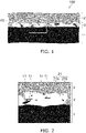
- FIG. 1 is a schematic cross-sectional view showing a bonded body according to an embodiment.
- the bonded body 100 includes a substrate 1, a metal member 2, and a bonding layer 3.
- the bonding layer 3 is located between the substrate 1 and the metal member 2.
- the substrate 1 includes at least one selected from the group consisting of silicon (Si) and aluminum (Al) and at least one selected from the group consisting of nitrogen (N), oxygen (O), and carbon (C).
- the substrate 1 may further include zirconium (Zr) and oxygen.
- the substrate 1 is, for example, a ceramic substrate.
- a silicon nitride substrate, an aluminum nitride substrate, an alumina substrate, a zirconia-including alumina substrate (an Alusil substrate), or a silicon carbide substrate can be used as the ceramic substrate.
- the three-point bending strength of the substrate 1 is not less than 500 MPa.
- the thickness of the substrate 1 can be reduced to be not more than 0.4 mm.
- a silicon nitride substrate, a high-strength aluminum nitride substrate, an alumina substrate, a zirconia-including alumina substrate, a silicon carbide substrate, etc. are examples of ceramic substrates having a three-point bending strength that is not less than 500 MPa.
- the silicon nitride substrate is favorable.
- a three-point bending strength that is not less than 500 MPa, and even not less than 600 MPa can be realized.
- the thermal cycle test characteristics the TCT characteristics
- a thermal conductivity that is not less than 50 W/m ⁇ K, and even not less than 80 W/m ⁇ K can be realized.
- the thickness of the substrate 1 also can be reduced to be not more than 0.30 mm by using a silicon nitride substrate having a three-point bending strength that is not less than 500 MPa and a thermal conductivity that is not less than 80 W/m ⁇ K.
- the three-point bending strength is measured according to JIS-R-1601.
- JIS-R-1601 corresponds to ISO 14704 (2000).
- the thermal conductivity is measured according to JIS-R-1611.
- the JIS-R-1611 corresponds to ISO 18755 (2005).
- the metal member 2 includes at least one selected from the group consisting of copper (Cu) and aluminum.
- the metal member 2 is, for example, a copper plate, a copper alloy plate, an aluminum plate, an aluminum alloy plate, etc. An element other than copper and aluminum may be included in these members.
- the metal member 2 may further include at least one selected from the group consisting of tungsten (W), nickel (Ni), molybdenum (Mo), and chromium (Cr).
- W tungsten
- Ni nickel
- Mo molybdenum
- Cr chromium
- the metal member 2 includes Cu-W-Ni, Cu-Mo, Cu-Cr, Cu-W, or Al-Si.
- the metal member 2 may include a cladding material made of at least two selected from Cu-W-Ni, Cu-Mo, Cu-Cr, Cu-W, and Al-Si.
- the metal member 2 may be patterned into an interconnect pattern. It is favorable for the thickness of the metal member 2 to be not less than 0.3 mm, and more favorably not less than 0.7 mm. By making the metal member 2 thick, the heat dissipation can be improved. The current-carrying capacity can be increased when the metal member 2 is used as a circuit.
- H is the heat transfer path.
- k is the thermal conductivity.
- A is the heat dissipation area.
- the bonding layer 3 can include a low melting-point metal.
- the melting point of the metal is less than the melting point of the substrate 1 and not more than the melting point of the metal member 2.
- the metal includes, for example, at least one selected from the group consisting of silver (Ag), copper, tin (Sn), and indium (In).
- the bonding layer 3 further includes an active metal and carbon. The flowability and the wetting of the brazing material when bonding can be suppressed by adding carbon.
- titanium (Ti) is used as the active metal. Titanium and at least one selected from the group consisting of zirconium and hafnium (Hf) may be used as the active metal.
- the bonding layer 3 includes copper, titanium, and carbon.
- the bonding layer 3 may further include silver. It is favorable for the content ratio of silver in the bonding layer 3 to be not less than 0 mass% and not more than 80 mass%. It is favorable for the content ratio of copper to be not less than 15 mass% and not more than 88 mass%. To increase the bonding strength, it is favorable for the content ratio of silver to be not less than 45 mass% and not more than 80 mass%, and for the content ratio of copper to be not less than 15 mass% and not more than 45 mass%. It is favorable for the content ratio of titanium to be not less than 1 mass% and not more than 12 mass%. It is favorable for the content ratio of carbon to be not less than 0.1 mass% and not more than 2 mass%.
- the bonding layer 3 includes at least one selected from tin (Sn) and indium (In), it is favorable for the content ratio of the at least one selected from tin (Sn) and indium (In) to be not less than 5 mass% and not more than 50 mass%. Tin (Sn) or indium (In) reduce the melting point of the bonding brazing material.
- the thickness of the bonding layer 3 is not less than 5 ⁇ m and not more than 60 ⁇ m.
- the thickness of the bonding layer 3 is less than 5 ⁇ m, there is a possibility that the unevenness of the substrate 1 surface may affect the surface of the bonding layer 3; and the uniform bonding between the bonding layer 3 and the substrate 1 may be obstructed.
- the thickness of the bonding layer 3 is greater than 60 ⁇ m, there is a possibility that the function of relaxing the thermal stress when subjected to thermal cycles may be insufficient, and the strength may decrease. Also, there is a possibility that it may be difficult to etch the bonding layer 3 when etching the metal member 2 and the bonding layer 3. Therefore, it is favorable for the thickness of the bonding layer 3 to be not less than 5 ⁇ m and not more than 60 ⁇ m, and more favorably not less than 10 ⁇ m and not more than 35 ⁇ m.
- the bonded body 100 is not limited to this example; multiple metal members 2 may be bonded to one surface of the substrate 1.
- One or more metal members 2 may be bonded to one surface of the substrate 1; and another one or more metal members 2 may be bonded to the surface on the opposite side of the substrate 1.
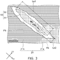
- FIG. 2 is an enlarged schematic cross-sectional view of a portion of the bonded body shown in FIG. 1.
- FIG. 2 is an enlarged view of portion P1 of FIG. 1 .
- the bonding layer 3 includes a first particle 11 and a first region 21.
- the first particle 11 includes carbon.
- the first region 21 includes a low melting-point metal.
- the first region 21 is disposed around the first particle 11.
- a powder body 10 which is described below, includes the first particle 11.
- the powder body 10 includes a second region 22 that is disposed around the first particle 11.
- the second region 22 of the powder body 10 contacts the first region 21.
- Multiple first particles 11 are provided in the first region 21. At least two of the multiple first particles 11 are separated from each other. For example, the first particles 11 are dispersed in the first region 21.
- the first region 21 includes, for example, a first partial region 21a that includes silver, and a second partial region 21b that includes copper.
- the first partial region 21a is a silver-rich phase that includes much silver.
- the content of silver in the first partial region 21a is greater than the content of copper in the first partial region 21a.
- the second partial region 21b is a copper-rich phase that includes much copper.
- the content of copper in the second partial region 21b is greater than the content of silver in the second partial region 21b.
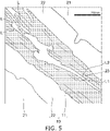
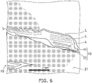
- FIGS. 3 , 6 , and 7 are schematic cross-sectional views showing portions of the bonded body according to the embodiment.
- FIGS. 4 and 5 are enlarged schematic cross-sectional views of portions of the bonded body shown in FIG. 3 .
- FIGS. 3 , 6 , and 7 are enlarged views of the first particle 11 vicinity.
- FIG. 4 is an enlarged view of portion P4 of FIG. 3 .
- FIG. 5 is an enlarged view of portion P5 of FIG. 3 .
- the second region 22 is disposed between the first particle 11 and the first region 21.
- the second region 22 exists around the first particle 11. That is, the first region 21 is disposed around the powder body 10 that includes the first particle 11 and the second region 22.
- the second region 22 surrounds the entire outer edge of the first particle 11.
- the second region 22 includes titanium and is disposed between the first particle 11 and the first region 21.
- a concentration a (mass%) of titanium in the second region 22 is greater than a concentration b (mass%) of titanium in the first region 21 and greater than a concentration c (mass%) of titanium in the first particle 11. That is, concentration a > concentration b, and concentration a > concentration c.
- the concentration c of titanium in the first particle 11 is not more than 50% of the concentration a of titanium in the second region 22, favorably not more than 25%, and more favorably not more than 10%. Also, the concentration b of titanium in the first region 21 is not more than 80% of the concentration a of titanium in the second region 22, favorably not more than 70%, and more favorably not more than 50%.
- the second region 22 includes multiple second particles 12.
- the first particle 11 is surrounded with the multiple second particles 12.
- At least one of the multiple second particles 12 includes at least one selected from the group consisting of titanium, oxygen, nitrogen, and carbon.
- at least one of the multiple second particles 12 includes a crystal including titanium and at least one selected from the group consisting of oxygen, nitrogen, and carbon.
- each second particle 12 is a crystal grain of titanium nitride, titanium oxide, titanium oxynitride, etc.
- the size of at least one of the multiple second particles 12 is less than the size of the first particle 11.
- the shape of the second particle 12 is granular.
- the shape of the second particle 12 may be a shape other than the illustrated shape such as a needle-like configuration, etc.
- the first particle 11 includes multiple layers L of carbon.
- the multiple layers L include a first layer L1 and a second layer L2.
- the first layer L1 and the second layer L2 may be separated from each other.
- a third region 23 is provided between the first layer L1 and the second layer L2.
- the third region 23 includes a low melting-point metal.
- the metallic element included in the third region 23 may be the same as the metallic element included in the first region 21.
- the third region 23 may include an element supplied from the substrate. That is, the third region 23 may include at least one element of the same type as an element included in the substrate. For example, when the first region 21 includes silver and copper, the third region 23 includes at least one selected from the group consisting of silver and copper.
- At least one of the multiple layers L is, for example, crystalline.
- the layer L includes, for example, a graphite crystal. Carbon is regularly ordered in the graphite crystal.
- the first layer L1 and the second layer L2 are disposed along a first direction D1.
- the shape of the first particle 11 is, for example, flattened as shown in FIG. 3 . There is also a possibility that the shape of the first particle 11 may be circular according to the position of the cross section.
- a length Le1 of the first particle 11 in the first direction D1 is, for example, not less than 1.2 times and not more than 40 times a length Le2 of the first particle 11 in a second direction D2 crossing the first direction D1.
- the second direction is the direction in which the length Le2 is shortest in one cross section.
- the method for measuring the lengths Le1 and Le2 of the first particle 11 and the calculation method of the ratio of the length Le1 to the length Le2 will now be described.
- the cross section of the bonding layer 3 is imaged using a scanning electron microscope (Scanning Electron Microscope; SEM) in an enlarged photograph having a unit area of 15 ⁇ m in the thickness direction ⁇ 100 ⁇ m in the surface direction.
- the thickness direction corresponds to the direction connecting the substrate 1 and the metal member 2.
- the surface direction is one direction perpendicular to the thickness direction.
- the magnification of the SEM photograph is set to "1000 times". For each of the first particles 11 visible in the SEM photograph, the distance between the two points most separated on the outer edge of the first particle 11 is taken as the length Le1.
- the length of the first particle 11 along a line segment that is perpendicular to a line segment connecting the two points and passing through the midpoint of the line segment is taken as the length Le2.
- the lengths Le1 and Le2 are measured for each of the first particles 11 observable in one field.
- the ratio ( Le1 / Le2 ) of the length Le1 to the length Le2 is calculated for the lengths Le1 and Le2 of each of the first particles 11. By performing this operation for three fields, the ratio of the length Le1 to the length Le2 is obtained for each of the fields.
- the average value of all of the ratios is the ratio of the length Le1 to the length Le2 of the bonded body 100.
- the ratio is not less than 1.2 and not more than 40.
- the second region 22 contacts the first partial region 21a.
- the second region 22 may contact the second partial region 21b, or may not contact the second partial region 21b.
- Multiple powder bodies 10 that are composite particles including the first particle 11 and the second region 22 are provided in the bonding layer 3. At least two of the multiple powder bodies 10 are separated from each other. For example, the powder bodies 10 are dispersed in the first region 21.
- the bonding layer 3 may include a fourth region 24 that includes titanium and nitrogen.
- the fourth region 24 is positioned between the substrate 1 and the first region 21.
- the powder body 10 may be separated from or may contact the fourth region 24.
- the ratio of the number of the powder bodies 10 separated from the fourth region 24 to the number of the powder bodies 10 contacting the fourth region 24 is not less than 9.0.
- a 30 ⁇ m ⁇ 200 ⁇ m region is observed by SEM; and the ratio is calculated based on the powder bodies 10 existing in the observation region.
- the observation region is set so that the fourth region 24 can be continuously confirmed from any one side to the side opposite to the one side.
- the first partial region 21a or the second partial region 21b is positioned between the powder body 10 and the fourth region 24.
- the bonding layer 3 may include a third particle 13.
- the third particle 13 includes at least one selected from the group consisting of titanium, silicon, and tin.
- the multiple third particles 13 are dispersed in the first region 21.
- the third particle 13 may contact the fourth region 24.
- the structures and the sizes of the first particle 11 and the second region 22 can be confirmed using SEM, a transmission electron microscope (Transmission Electron Microscope; TEM), or a scanning transmission electron microscope (Scanning Transmission Electron Microscope; STEM).
- the elements and the concentrations of the elements included in the first particle 11, the first region 21, and the second region 22 can be confirmed using elemental mapping by STEM.
- the bonded body 100 according to the embodiment is manufactured by the following method.
- the substrate 1 is prepared.
- a brazing material paste is coated onto the upper surface of the substrate 1.
- the brazing material paste includes silver, copper, titanium, and carbon.
- the metal member 2 is disposed on the brazing material paste. It is favorable for the thickness of the brazing material paste to be not less than 5 ⁇ m and not more than 60 ⁇ m, and more favorably not less than 10 ⁇ m and not more than 40 ⁇ m. When the coating thickness is less than 5 ⁇ m, there is a possibility that the brazing material may be insufficient; and the bonding strength may decrease. When the coating thickness is greater than 60 ⁇ m, the coating difficulty increases, and it becomes difficult to coat the brazing material paste with high uniformity.
- the brazing material paste is coated onto both the upper surface and the lower surface of the substrate 1.
- the substrate 1 on which the metal member 2 is provided is heated. Initially, heating is performed to the vicinity of 500 °C at a pressure 13.3 Pa in a nitrogen atmosphere. The substrate 1 is heated for not less than 30 minutes by holding the temperature in the range of 480 °C to 500 °C. At this time, the binding component that is included in the brazing material paste melts; and carbon remains without melting. Particles that include titanium cluster around the remaining carbon. Thereby, multiple particles that include titanium are disposed around particles including carbon. It is favorable for the pressure in the nitrogen atmosphere to be in the range not less than 0.01 Pa and not more than atmospheric pressure. Atmospheric pressure is 1 atmosphere (0.101325 MPa). It is more favorable for the pressure to be not less than 5 Pa.
- the nitrogen atmosphere refers to the nitrogen concentration in the gas existing in the processing space being not less than 50 vol%. It is favorable for the nitrogen concentration in the nitrogen atmosphere to be not less than 70 vol%.
- the nitrogen atmosphere may include an inert gas such as oxygen or a noble gas.
- the nitrogen atmosphere may be obtained by depressurizing air. At least a portion of the air may be replaced with nitrogen gas or a gas mixture of nitrogen gas and noble gas.
- the percentage of the noble gas to the gas other than nitrogen in the nitrogen atmosphere is not less than 0.5 vol%.
- the pressure is depressurized to be not more than 10 -3 Pa.
- the substrate 1 is heated for not less than 30 minutes by holding the temperature in the range from 550 °C to 600 °C.
- the multiple particles that include titanium are stabilized by this processing.
- the substrate 1 is heated for not less than 10 minutes, and favorably not less than 30 minutes by holding the temperature in a range from 700 °C to 950 °C.
- the metal that is included in the brazing material paste is melted thereby, and the substrate 1 and the metal member 2 are bonded.
- an etching process of the metal member 2 may be performed.
- the metal member 2 is patterned by the etching process.
- one or more metal members 2 that are bonded to the substrate 1 are patterned into a patterned configuration (a circuit configuration).
- FIG. 8 is a schematic cross-sectional view showing a portion of the bonded body according to the embodiment.
- FIG. 8 shows an example of the metal member 2 after patterning.
- the substrate 1 includes a first surface S1.
- the metal member 2 is bonded to the first surface S1 via the bonding layer 3.
- a side surface 2S of the metal member 2 after the patterning is oblique to a third direction D3 perpendicular to the first surface S1 as shown in FIG. 8 .
- a portion of the bonding layer 3 not to be interposed between the substrate 1 and the metal member 2 in the third direction D3.
- the bonding layer 3 it is favorable for the bonding layer 3 to include a jutting portion 3J that juts from between the substrate 1 and the metal member 2. Because the side surface 2S is oblique and the jutting portion 3J is provided, the stress of the substrate 1 and the metal member 2 can be relaxed. The TCT characteristics can be improved thereby.
- a length W of the jutting portion 3J in a fourth direction D4 crossing the third direction D3 is not less than 10 ⁇ m and not more than 150 ⁇ m.
- the fourth direction D4 is parallel to the first surface S1.
- the ratio of the length W of the jutting portion 3J to a thickness T of the jutting portion 3J is not less than 0.5 and not more than 3.0. More favorably, the ratio of the length W to the thickness T is not less than 1.0 and not more than 2.0.
- the thickness T of the jutting portion 3J corresponds to the length in the third direction D3 of the jutting portion 3J.
- the metal member 2 contacts the bonding layer 3 at a contact surface CS.
- a line segment that passes through the thickness direction (the third direction D3) center of the metal member 2 is taken as a center line CL.
- the center line CL crosses the side surface 2S at an intersection IS.
- a slope angle ⁇ 1 of the side surface 2S is represented by the angle with respect to the third direction D3 of a line segment connecting the intersection IS and the end portion of the contact surface CS. It is favorable for the slope angle ⁇ 1 to be not less than 40 degrees and not more than 84 degrees.
- an angle ⁇ 2 of the upper end portion of the metal member 2 is not less than 85 degrees and not more than 95 degrees.
- the angle ⁇ 2 is represented by the angle between the side surface 2S and an upper surface 2U of the metal member 2. This structure is particularly effective when the thickness of the metal member 2 is not less than 0.6 mm, and more effective when not less than 0.8 mm.
- the slope angle ⁇ 1 to be 40 to 84 degrees and the angle ⁇ 2 to be 85 to 95 degrees
- the surface area of the flat upper surface 2U can be increased while relaxing the stress.
- the surface area on which semiconductor elements can be mounted can be wide.
- the degrees of freedom of the circuit design can be increased.
- the bonded body according to the embodiment is favorable for a circuit board.
- the weak portions are initially fractured.
- a ceramic substrate that has a three-point bending strength that is not less than 500 MPa as the substrate 1, the occurrence of cracks in the substrate 1 can be suppressed.
- the strength of the substrate 1 is low, cracks easily occur in the substrate 1 due to the thermal stress.
- the substrate 1 includes a nitride material, titanium nitride is formed when bonding by a reaction of the nitrogen of the substrate 1 and the titanium of the bonding layer 3.
- the bonding strength of the bonded body 100 can be increased by the formation of titanium nitride.
- the bonding strength of the bonded body 100 can be increased by the melting and diffusing at the interface between the metal member 2 and the bonding layer 3 when bonding.
- the bonding at the interface of the bonding layer 3 is strong, the thermal stress concentrates in the bonding layer 3 interior. Therefore, it is desirable for the strength of the bonding layer 3 to be high.
- the bonding layer 3 includes the first particle 11, the first region 21, and the second region 22.
- the first particle 11 includes carbon.
- the wettability of carbon with metal is not good. In other words, the wettability of the first particle 11 with the first region 21 is not good.
- locations where the wettability is poor exist inside the bonding layer 3 voids may occur at such locations and may become starting points of cracks. As a result, there is a possibility that the strength of the bonding layer 3 may decrease.
- the second region 22 that includes titanium is disposed between the first particle 11 and the first region 21.
- the second region 22 includes an element supplied from the substrate 1 such as nitrogen, oxygen, carbon, etc. Therefore, much of the titanium exists not in a metal form, but in the form of an inorganic substance such as an oxide, a nitride, an oxynitride, a carbide, etc.
- an inorganic substance such as an oxide, a nitride, an oxynitride, a carbide, etc.
- the second region 22 is disposed around the first particle 11.
- the second region 22 includes the multiple second particles 12.
- the first particle 11 and the multiple second particles 12 form one aggregate as the powder body 10.
- the second region 22 When one cross section of the bonding layer 3 is observed, it is favorable for the second region 22 to cover not less than 90% of the surface of the first particle 11. More favorably, the second region 22 covers not less than 95% of the surface of the first particle 11. Because the second region 22 covers a wider area of the surface of the first particle 11, the occurrence of voids around the first particle 11 can be suppressed. The strength of the bonding layer 3 is increased thereby.
- the thickness of the second region 22 is not less than 2 nm and not more than 1 ⁇ m. More favorably, the thickness of the second region 22 is not less than 10 nm and not more than 500 nm. When the thickness is less than 2 nm, the effect of improving the wettability weakens. Also, to form the second region 22 to have a thickness greater than 1 ⁇ m, it is necessary for the titanium component to be plentiful. When a plentiful titanium component is used in the formation of the second region 22, there is a possibility that the titanium nitride layer formed at the interface between the substrate 1 and the bonding layer 3 may become thin, and the bonding strength between the substrate 1 and the bonding layer 3 may decrease.
- the content ratio of titanium in the second region 22 is not less than 50 mass%. More favorably, the content ratio of titanium in the second region 22 is not less than 60 mass%. It is favorable for the second region 22 to include titanium and nitrogen.
- at least one second particle 12 included in the second region 22 includes titanium and nitrogen.
- the second particle 12 may further include oxygen.
- at least one second particle 12 includes a crystal including titanium and at least one selected from the group consisting of nitrogen and oxygen. Because the second particle 12 includes a crystal, the stress that is generated in the bonding layer 3 can be relaxed.
- the second region 22 is disposed around each of the multiple first particles 11. It is favorable for the percentage of the number of the first particles 11 around which the second region 22 is not provided to the total number of the first particles 11 in one cross section to be not more than 5%. More favorably, the percentage is not more than 3%. When the percentage is greater than 5%, there is a possibility that voids may easily occur, and the strength of the bonding layer 3 may decrease.
- the thickness direction corresponds to the third direction D3 shown in FIG. 8 .
- the surface direction corresponds to the fourth direction D4 shown in FIG. 8 .
- the strength of the bonding layer 3 can be further increased as the number of the powder bodies 10 is increased.
- FIGS. 9A to 9C are schematic cross-sectional views showing bonded bodies according to the embodiment.
- a bonded body 110 shown in FIG. 9A includes the substrate 1, the multiple metal members 2, and the multiple bonding layers 3.
- the multiple metal members 2 include a first metal member 2a, a second metal member 2b, and a third metal member 2c.
- the multiple bonding layers 3 include a first bonding layer 3a, a second bonding layer 3b, and a third bonding layer 3c.
- the substrate 1 includes the first surface S1 and a second surface S2.
- the first metal member 2a is separated from the second metal member 2b in the second direction D2 along the first surface S1.
- the first metal member 2a may be linked to the second metal member 2b at a not-illustrated portion.
- the first metal member 2a and the second metal member 2b are bonded to the first surface S1 respectively via the first bonding layer 3a and the second bonding layer 3b.
- the third metal member 2c is bonded to the second surface S2 via the third bonding layer 3c.
- a bonded body 120 shown in FIG. 9B further includes a fourth metal member 2d, a first connector 4a, and a second connector 4b.
- the third metal member 2c is separated from the fourth metal member 2d in the second direction D2.
- the third metal member 2c may be linked to the fourth metal member 2d at a not-illustrated portion.
- the fourth metal member 2d is bonded to the second surface S2 via the third bonding layer 3c.
- the first connector 4a and the second connector 4b are located in the substrate 1.
- the first connector 4a is located between the first bonding layer 3a and the third bonding layer 3c in the first direction D1 and is electrically connected with these bonding layers.
- the second connector 4b is located between the second bonding layer 3b and the third bonding layer 3c in the first direction D1 and is electrically connected with these bonding layers.
- FIG. 9C shows a semiconductor device 210 that uses the bonded body 110 according to the embodiment.
- the semiconductor device 210 includes the bonded body 110, a semiconductor element 5, and a bonding layer 6a.
- the semiconductor element 5 is bonded to the first metal member 2a via the bonding layer 6a.
- the first metal member 2a is positioned between the substrate 1 and the semiconductor element 5 in the first direction D1.
- the semiconductor device 210 may further include a bonding wire 7 and a metal terminal 8.
- the metal terminal 8 is bonded to the second metal member 2b via a bonding layer 6b.
- the second metal member 2b is positioned between the substrate 1 and the metal terminal 8 in the first direction D1.
- the bonding wire 7 connects the first metal member 2a and the second metal member 2b.
- the compositions and the structures of the bonding layers 6a and 6b may be the same as or different from the composition and the structure of the bonding layer 3.
- Table 1 Material Substrate size(mm) Three-point bending strength(MPa) Substrate A Silicon nitride 50 ⁇ 40 ⁇ 0.3 620 Substrate B Silicon nitride 50 ⁇ 40 ⁇ 0.25 710
- brazing material component (mass%) Brazing material 1 Ag (70), Cu (29), Ti (1) Brazing material 2 Ag(61),Cu(24),In(8.5),Ti(5),C(1.5) Brazing material 3 Ag(50),Cu(28),Sn(11),In(3),Ti(7),C(1) Brazing material 4 Ag(47.5),Cu(37),Sn(7),Ti(8),C(0.5) Brazing material 5 Ag(47.5),Cu(36.5),Sn(7),Ti(8),C(1) Brazing material 6 Ag(50)),Cu(28.9),Sn(11),In(3),Ti(7),C(0.1)
- a copper plate having a thickness of 0.8 mm is used as the metal member 2.
- a brazing material paste is coated onto the upper surface and the lower surface of the substrate 1.
- the thickness of the brazing material paste is 25 ⁇ m.
- Metal members are disposed at and bonded to the upper surface and the lower surface.
- the metal member that is disposed at the upper surface is patterned by etching.
- the heat treatment when bonding the substrate 1 and the metal member 2 is performed using the following seven conditions.
- the atmosphere, the pressure, and the holding time when holding the temperature of the substrate 1 at about 600 °C are common to the heat treatment condition 2. Also, the atmosphere and the pressure when holding the temperature of the substrate 1 at not less than 700 °C and not more than 850 °C are common to the heat treatment condition 2. For the heat treatment condition 7, the temperature of the substrate 1 is held to be not less than 850 °C and not more than 950 °C.
- the substrate 1 is heated for 30 minutes by holding the temperature of the substrate 1 at not less than 700 °C and not more than 850 °C in a non-oxidative atmosphere that is not more than 1 ⁇ 10 -3 Pa.
- the non-oxidative atmosphere refers to the oxygen concentration in the gas existing in the processing space being not more than 25 vol%.
- the substrate 1 is heated for 30 minutes by holding the temperature of the substrate 1 at about 500 °C in a nitrogen atmosphere of 13.3 Pa.
- the nitrogen concentration in the nitrogen atmosphere is 90 vol%.
- the substrate 1 is heated for 120 minutes by holding the temperature of the substrate 1 at about 600 °C in a non-oxidative atmosphere that is not more than 1 ⁇ 10 -3 Pa.
- the substrate 1 is heated for 30 minutes by holding the temperature of the substrate 1 at not less than 700 °C and not more than 850 °C in a non-oxidative atmosphere that is not more than 1 ⁇ 10 -3 Pa.
- the substrate 1 is heated for 30 minutes by holding the temperature of the substrate 1 at about 500 °C in a nitrogen atmosphere of 0.01 Pa.
- the nitrogen concentration in the nitrogen atmosphere is 99.9 vol%.
- the substrate 1 is heated for 30 minutes by holding the temperature of the substrate 1 at not less than 700 °C and not more than 850 °C.
- the substrate 1 is heated for 60 minutes by holding the temperature of the substrate 1 at about 500 °C in a nitrogen atmosphere of 0.5 Pa.
- the nitrogen concentration in the nitrogen atmosphere is 70 vol%.
- the substrate 1 is heated for 30 minutes by holding the temperature of the substrate 1 at not less than 700 °C and not more than 850 °C.
- the substrate 1 is heated for 120 minutes by holding the temperature of the substrate 1 at about 500 °C in a nitrogen atmosphere of 0.03 Pa.
- the nitrogen concentration in the nitrogen atmosphere is 80 vol%.
- the substrate 1 is heated for 120 minutes by holding the temperature of the substrate 1 at not less than 700 °C and not more than 850 °C.
- the substrate 1 is heated for 150 minutes by holding the temperature of the substrate 1 at about 500 °C in a nitrogen atmosphere of 5 Pa.
- the nitrogen concentration in the nitrogen atmosphere is 70 vol%.
- the substrate 1 is heated for 200 minutes by holding the temperature of the substrate 1 at not less than 700 °C and not more than 850 °C.
- the substrate 1 is heated for 150 minutes by holding the temperature of the substrate 1 at about 500 °C in a nitrogen atmosphere of 5 Pa.
- the nitrogen concentration in the nitrogen atmosphere is 90 vol%.
- the substrate 1 is heated for 100 minutes by holding the temperature of the substrate 1 at not less than 860 °C and not more than 950 °C.
- the combinations of the type of the substrate 1, the type of the brazing material, and the type of the heat treatment condition are as shown in Table 4.
- Table 4 Substrate Brazing material composition Heat treatment condition Example 1 Substrate A Brazing material 2 Heat treatment 2 Example 2 Substrate A Brazing material 3 Heat treatment 2 Example 3 Substrate A Brazing material 4 Heat treatment 2 Example 4 Substrate B Brazing material 2 Heat treatment 2 Example 5 Substrate B Brazing material 3 Heat treatment 2 Example 6 Substrate B Brazing material 4 Heat treatment 2 Example 7 Substrate A Brazing material 1 Heat treatment 1 Example 8 Substrate A Brazing material 5 Heat treatment 3 Example 9 Substrate A Brazing material 5 Heat treatment 4 Example 10 Substrate A Brazing material 6 Heat treatment 5 Example 11 Substrate A Brazing material 6 Heat treatment 6 Example 12 Substrate A Brazing material 6 Heat treatment 7
- a peel strength was measured and TCT was performed for the bonded bodies according to the examples.
- the peel strength was measured by bonding the metal member 2 having a width of 1 mm to the substrate 1 and by pulling the metal member 2 in the vertical direction.
- TCT the existence or absence of discrepancies was measured for the bonded bodies after 5000 cycles. In one cycle, hold for 30 minutes at -50 °C ⁇ hold for 10 minutes at room temperature ⁇ hold for 30 minutes at 200 °C ⁇ hold for 10 minutes at room temperature were performed.
- the discrepancies of the bonded bodies were determined by using an ultrasonic flaw detection device (Scanning Acoustic Tomograph: SAT) of the crack occurrence area between the substrate 1 and the metal member 2. The crack occurrence area was evaluated using an index ⁇ .
- SAT Ultrasonic flaw detection device
- the brazing materials 2 to 4 further include carbon (C).
- C carbon
- the inventors conjectured that carbon contributes to the improvement of the characteristics. Based on this conjecture, the inventors performed observations of the particles that include carbon in the bonding layer 3.
- Table 6 shows the results of electron microscope observations of the cross section of the bonding layer 3 for each of the examples 1 to 7. The number of powder bodies was measured in a 15 ⁇ m ⁇ 100 ⁇ m area.
- the thickness shown in Table 6 is the thickness of the second region 22.
- the thickness of the second region 22 is measured by the following method. The thickness of the second region 22 existing around each first particle 11 is measured in one direction from the first particle 11 toward the first region 21. The direction is randomly determined. The thickness of each second region 22 is measured as follows. An AMC cross section is patterned and observed by TEM. Three locations of the second region 22 are randomly selected as the measurement locations. The thicknesses of the measurement locations are measured, and the average value of the thicknesses is taken as the "thickness of the second region 22".
- the coverage is measured by the following method. The percentage of the length of the outer circumference contacting the second region 22 to the length of the outer circumference is calculated for each first particle 11. The percentages of the first particles 11 are averaged and taken as the "coverage".
- Composition analysis of the second region 22 was performed by STEM-EDS for the bonded bodies according to the specific examples.
- the Ti concentration in the second region 22 was not less than 50 wt% for each of the specific examples.
- Ti, N, and O were detected at each of the measurement points.
- the second region 22 was a cluster of microcrystals. Carbon was detected in the microcrystals.
- the powder body 10 is confirmed in the bonding layer 3 when using brazing materials including carbon.
- the first particle 11 that includes carbon and the second region 22 that includes titanium exist in the bonding layer 3.
- the first particle 11 is surrounded with the second region 22. It is considered that by providing the powder body 10 having such a structure, the strength of the bonded body is increased, and the occurrence of cracks is suppressed.
- the ratio of the length Le1 to the length Le2 of the first particle 11 is within the range not less than 1.2 and not more than 40 for the bonded bodies according to the specific examples.
- a bonded body can be provided in which the bonding strength can be increased.
- perpendicular and parallel include not only strictly perpendicular and strictly parallel but also, for example, the fluctuation of manufacturing processes, etc.; and it is sufficient to be substantially perpendicular and substantially parallel.
Landscapes
- Engineering & Computer Science (AREA)
- Chemical & Material Sciences (AREA)
- Mechanical Engineering (AREA)
- Materials Engineering (AREA)
- Ceramic Engineering (AREA)
- Structural Engineering (AREA)
- Organic Chemistry (AREA)
- Ceramic Products (AREA)
- Manufacturing Of Printed Wiring (AREA)
- Parts Printed On Printed Circuit Boards (AREA)
- Pressure Welding/Diffusion-Bonding (AREA)
Applications Claiming Priority (2)
| Application Number | Priority Date | Filing Date | Title |
|---|---|---|---|
| JP2019159468 | 2019-09-02 | ||
| PCT/JP2020/031407 WO2021044854A1 (ja) | 2019-09-02 | 2020-08-20 | 接合体、回路基板、及び半導体装置 |
Publications (2)
| Publication Number | Publication Date |
|---|---|
| EP4026819A1 true EP4026819A1 (de) | 2022-07-13 |
| EP4026819A4 EP4026819A4 (de) | 2023-12-06 |
Family
ID=74852458
Family Applications (1)
| Application Number | Title | Priority Date | Filing Date |
|---|---|---|---|
| EP20861301.8A Pending EP4026819A4 (de) | 2019-09-02 | 2020-08-20 | Zusammengesetzter körper, leiterplatte und halbleiterbauelement |
Country Status (5)
| Country | Link |
|---|---|
| US (1) | US11948900B2 (de) |
| EP (1) | EP4026819A4 (de) |
| JP (2) | JP7240511B2 (de) |
| CN (1) | CN113508462B (de) |
| WO (1) | WO2021044854A1 (de) |
Families Citing this family (6)
| Publication number | Priority date | Publication date | Assignee | Title |
|---|---|---|---|---|
| CN113508462B (zh) * | 2019-09-02 | 2024-09-20 | 株式会社东芝 | 接合体、电路基板及半导体装置 |
| WO2021111508A1 (ja) * | 2019-12-03 | 2021-06-10 | 日本碍子株式会社 | 接合基板及び接合基板の製造方法 |
| JP2023013631A (ja) | 2021-07-16 | 2023-01-26 | 三菱マテリアル株式会社 | 銅/セラミックス接合体、絶縁回路基板、および、銅/セラミックス接合体の製造方法、絶縁回路基板の製造方法 |
| JP7642930B1 (ja) * | 2023-05-19 | 2025-03-10 | 株式会社東芝 | 熱処理炉装置 |
| TWI850011B (zh) * | 2023-07-06 | 2024-07-21 | 同欣電子工業股份有限公司 | 含有鋁元素的活性金屬硬焊基板材料及其製造方法 |
| JP7734345B1 (ja) | 2024-02-20 | 2025-09-05 | 株式会社Niterra Materials | セラミックス封着部品およびその製造方法 |
Family Cites Families (28)
| Publication number | Priority date | Publication date | Assignee | Title |
|---|---|---|---|---|
| JP3095490B2 (ja) * | 1991-11-29 | 2000-10-03 | 株式会社東芝 | セラミックス−金属接合体 |
| JPH05319946A (ja) * | 1992-05-22 | 1993-12-03 | Ibiden Co Ltd | 金属板接合セラミック基板 |
| JP4077888B2 (ja) * | 1995-07-21 | 2008-04-23 | 株式会社東芝 | セラミックス回路基板 |
| JP3834351B2 (ja) | 1996-04-09 | 2006-10-18 | 株式会社東芝 | セラミックス回路基板 |
| JPH10158073A (ja) * | 1996-11-25 | 1998-06-16 | Sumitomo Kinzoku Erekutorodebaisu:Kk | セラミックス基板と金属板との接合方法 |
| JP4574951B2 (ja) * | 2003-02-26 | 2010-11-04 | 株式会社東芝 | 半導体装置及びその製造方法 |
| CN100528810C (zh) * | 2007-09-11 | 2009-08-19 | 西安交通大学 | 一种ZrO2陶瓷与不锈钢或Al2O3陶瓷无压钎焊的方法 |
| CN101468799B (zh) * | 2007-09-11 | 2010-11-10 | 西安交通大学 | 一种ZrO2陶瓷与Al2O3陶瓷无压钎焊的方法 |
| US9012783B2 (en) | 2009-05-27 | 2015-04-21 | Kyocera Corporation | Heat dissipation base and electronic device |
| EP3273755B1 (de) | 2009-09-15 | 2018-11-07 | Kabushiki Kaisha Toshiba | Verfahren zur herstellung einer keramikleiterplatte |
| US9425146B2 (en) * | 2010-09-28 | 2016-08-23 | Infineon Technologies Ag | Semiconductor structure and method for making same |
| WO2012058656A2 (en) * | 2010-10-29 | 2012-05-03 | Ritedia Corporation | Stress regulated semiconductor and associated methods |
| JP5743503B2 (ja) | 2010-11-29 | 2015-07-01 | 京セラ株式会社 | ろう材およびこれを用いた回路基板ならびに電子装置 |
| CN103429375B (zh) * | 2011-03-25 | 2016-10-26 | 日本碍子株式会社 | 碳化钨基硬质合金接合体及其制造方法 |
| JP5472529B2 (ja) * | 2011-03-31 | 2014-04-16 | 日立ツール株式会社 | 硬質皮膜被覆部材及びそれを具備する刃先交換式回転工具 |
| CN104011852B (zh) * | 2011-12-20 | 2016-12-21 | 株式会社东芝 | 陶瓷铜电路基板和使用了陶瓷铜电路基板的半导体装置 |
| JP2014118310A (ja) * | 2012-12-14 | 2014-06-30 | Denki Kagaku Kogyo Kk | セラミックス回路基板 |
| JP6430382B2 (ja) | 2013-08-08 | 2018-11-28 | 株式会社東芝 | 回路基板および半導体装置 |
| EP3053899B1 (de) * | 2013-09-30 | 2019-11-06 | Mitsubishi Materials Corporation | Cu/keramikmaterialverbindung, verfahren zur herstellung einer cu/keramikmaterialverbindung und substrat für leistungsmodul |
| JP6416776B2 (ja) * | 2013-11-15 | 2018-10-31 | 住友電工ハードメタル株式会社 | ダイヤモンド接合体、それを備える工具、およびダイヤモンド接合体の製造方法 |
| WO2015125907A1 (ja) | 2014-02-21 | 2015-08-27 | 電気化学工業株式会社 | セラミックス回路基板 |
| JP5972317B2 (ja) * | 2014-07-15 | 2016-08-17 | 株式会社マテリアル・コンセプト | 電子部品およびその製造方法 |
| JP6307386B2 (ja) | 2014-08-20 | 2018-04-04 | デンカ株式会社 | セラミックス回路基板 |
| EP3492441B1 (de) | 2016-07-28 | 2024-10-16 | Kabushiki Kaisha Toshiba | Verbundener körper, leiterplatte und halbleiterbauelement |
| JP6799790B2 (ja) * | 2016-12-06 | 2020-12-16 | パナソニックIpマネジメント株式会社 | 接合材とそれにより得られる接合体と接合体の製造方法 |
| JP6965768B2 (ja) * | 2017-02-28 | 2021-11-10 | 三菱マテリアル株式会社 | 銅/セラミックス接合体、絶縁回路基板、及び、銅/セラミックス接合体の製造方法、絶縁回路基板の製造方法 |
| US10629686B2 (en) * | 2018-08-02 | 2020-04-21 | Semiconductor Components Industries, Llc | Carbon-controlled ohmic contact layer for backside ohmic contact on a silicon carbide power semiconductor device |
| CN113508462B (zh) * | 2019-09-02 | 2024-09-20 | 株式会社东芝 | 接合体、电路基板及半导体装置 |
-
2020
- 2020-08-20 CN CN202080018277.0A patent/CN113508462B/zh active Active
- 2020-08-20 EP EP20861301.8A patent/EP4026819A4/de active Pending
- 2020-08-20 JP JP2021543688A patent/JP7240511B2/ja active Active
- 2020-08-20 WO PCT/JP2020/031407 patent/WO2021044854A1/ja not_active Ceased
-
2021
- 2021-09-02 US US17/446,765 patent/US11948900B2/en active Active
-
2022
- 2022-11-25 JP JP2022188028A patent/JP7471376B2/ja active Active
Also Published As
| Publication number | Publication date |
|---|---|
| US20210398928A1 (en) | 2021-12-23 |
| WO2021044854A1 (ja) | 2021-03-11 |
| JP7240511B2 (ja) | 2023-03-15 |
| US11948900B2 (en) | 2024-04-02 |
| CN113508462B (zh) | 2024-09-20 |
| JP2023052728A (ja) | 2023-04-12 |
| CN113508462A (zh) | 2021-10-15 |
| EP4026819A4 (de) | 2023-12-06 |
| JPWO2021044854A1 (de) | 2021-03-11 |
| JP7471376B2 (ja) | 2024-04-19 |
Similar Documents
| Publication | Publication Date | Title |
|---|---|---|
| EP4026819A1 (de) | Zusammengesetzter körper, leiterplatte und halbleiterbauelement | |
| CN102612745B (zh) | 电子设备用散热板及其制造方法 | |
| CN102027592B (zh) | 功率模块用基板、功率模块及功率模块用基板的制造方法 | |
| EP3109222B1 (de) | Keramikleiterplatte | |
| JP5524905B2 (ja) | パワー半導体素子用Al合金膜 | |
| EP3236495B1 (de) | Schaltungssubstrat und elektronische vorrichtung | |
| US20160152004A1 (en) | Composite laminate and electronic device | |
| US12120852B2 (en) | Composite material and heat dissipation part | |
| JPH09157054A (ja) | 回路基板 | |
| TW201336598A (zh) | 銀-金-鈀合金表面鍍金屬薄膜之複合線材及其製法 | |
| TW201809299A (zh) | 用於功率模組封裝之金屬帶材 | |
| CN116018884A (zh) | 接合体及采用其的陶瓷电路基板以及半导体装置 | |
| EP4053091A1 (de) | Kupfer-/keramikanordnung, isolierte leiterplatte, verfahren zur herstellung einer kupfer-/keramikanordnung und verfahren zur herstellung einer isolierten leiterplatte | |
| US20250098065A1 (en) | Bonded body and ceramic circuit board using same | |
| KR102884605B1 (ko) | 복합재료 및 이 복합재료를 포함하는 방열부품 | |
| WO2024195792A1 (ja) | 静電チャック装置 | |
| EP4074678B1 (de) | Kupfer-/keramikanordnung und isolierte leiterplatte | |
| EP4043203B1 (de) | Verbundsubstrat und verfahren zu seiner herstellung und schaltungssubstrat und verfahren zu seiner herstellung | |
| EP4234518A1 (de) | Verbundener körper, keramik-kupfer-leiterplatte und halbleiterbauelement | |
| EP4328208A1 (de) | Kupfer/keramik verbundkörper und isolierte leiterplatte | |
| JP4720326B2 (ja) | スパッタリング用Ti−Wターゲット | |
| KR102220725B1 (ko) | 브레이징 필러 금속, 브레이징 필러 합금 판재 및 브레이징 접합 방법 | |
| JP2026008239A (ja) | 静電チャック装置、静電チャック装置の製造方法及び積層体の製造方法 | |
| WO2026062995A1 (ja) | 接合体および半導体製造装置 | |
| JP2026073987A (ja) | サセプター及びその製造方法 |
Legal Events
| Date | Code | Title | Description |
|---|---|---|---|
| STAA | Information on the status of an ep patent application or granted ep patent |
Free format text: STATUS: THE INTERNATIONAL PUBLICATION HAS BEEN MADE |
|
| PUAI | Public reference made under article 153(3) epc to a published international application that has entered the european phase |
Free format text: ORIGINAL CODE: 0009012 |
|
| STAA | Information on the status of an ep patent application or granted ep patent |
Free format text: STATUS: REQUEST FOR EXAMINATION WAS MADE |
|
| 17P | Request for examination filed |
Effective date: 20210902 |
|
| AK | Designated contracting states |
Kind code of ref document: A1 Designated state(s): AL AT BE BG CH CY CZ DE DK EE ES FI FR GB GR HR HU IE IS IT LI LT LU LV MC MK MT NL NO PL PT RO RS SE SI SK SM TR |
|
| DAV | Request for validation of the european patent (deleted) | ||
| DAX | Request for extension of the european patent (deleted) | ||
| A4 | Supplementary search report drawn up and despatched |
Effective date: 20231106 |
|
| RIC1 | Information provided on ipc code assigned before grant |
Ipc: B23K 35/30 20060101ALI20231030BHEP Ipc: B23K 35/02 20060101ALI20231030BHEP Ipc: H01L 23/00 20060101ALI20231030BHEP Ipc: H01L 23/498 20060101ALI20231030BHEP Ipc: H01L 23/15 20060101ALI20231030BHEP Ipc: B23K 103/00 20060101ALI20231030BHEP Ipc: B23K 103/18 20060101ALI20231030BHEP Ipc: B23K 103/12 20060101ALI20231030BHEP Ipc: B23K 103/10 20060101ALI20231030BHEP Ipc: B23K 101/42 20060101ALI20231030BHEP Ipc: B23K 1/00 20060101ALI20231030BHEP Ipc: H01L 23/13 20060101ALI20231030BHEP Ipc: B23K 1/19 20060101ALI20231030BHEP Ipc: C04B 37/02 20060101AFI20231030BHEP |
|
| RAP1 | Party data changed (applicant data changed or rights of an application transferred) |
Owner name: NITERRA MATERIALS CO., LTD. |