EP4044229A2 - Collier de barrière de diffusion pour interconnexions - Google Patents
Collier de barrière de diffusion pour interconnexions Download PDFInfo
- Publication number
- EP4044229A2 EP4044229A2 EP22166588.8A EP22166588A EP4044229A2 EP 4044229 A2 EP4044229 A2 EP 4044229A2 EP 22166588 A EP22166588 A EP 22166588A EP 4044229 A2 EP4044229 A2 EP 4044229A2
- Authority
- EP
- European Patent Office
- Prior art keywords
- substrate
- conductive interconnect
- interconnect structure
- conductive
- barrier interface
- Prior art date
- Legal status (The legal status is an assumption and is not a legal conclusion. Google has not performed a legal analysis and makes no representation as to the accuracy of the status listed.)
- Pending
Links
Images




Classifications
-
- H—ELECTRICITY
- H10—SEMICONDUCTOR DEVICES; ELECTRIC SOLID-STATE DEVICES NOT OTHERWISE PROVIDED FOR
- H10W—GENERIC PACKAGES, INTERCONNECTIONS, CONNECTORS OR OTHER CONSTRUCTIONAL DETAILS OF DEVICES COVERED BY CLASS H10
- H10W20/00—Interconnections in chips, wafers or substrates
- H10W20/01—Manufacture or treatment
- H10W20/071—Manufacture or treatment of dielectric parts thereof
- H10W20/074—Manufacture or treatment of dielectric parts thereof of dielectric parts comprising thin functional dielectric layers, e.g. dielectric etch-stop, barrier, capping or liner layers
- H10W20/076—Manufacture or treatment of dielectric parts thereof of dielectric parts comprising thin functional dielectric layers, e.g. dielectric etch-stop, barrier, capping or liner layers in via holes or trenches
-
- H—ELECTRICITY
- H10—SEMICONDUCTOR DEVICES; ELECTRIC SOLID-STATE DEVICES NOT OTHERWISE PROVIDED FOR
- H10W—GENERIC PACKAGES, INTERCONNECTIONS, CONNECTORS OR OTHER CONSTRUCTIONAL DETAILS OF DEVICES COVERED BY CLASS H10
- H10W70/00—Package substrates; Interposers; Redistribution layers [RDL]
- H10W70/60—Insulating or insulated package substrates; Interposers; Redistribution layers
- H10W70/611—Insulating or insulated package substrates; Interposers; Redistribution layers for connecting multiple chips together
-
- H—ELECTRICITY
- H10—SEMICONDUCTOR DEVICES; ELECTRIC SOLID-STATE DEVICES NOT OTHERWISE PROVIDED FOR
- H10P—GENERIC PROCESSES OR APPARATUS FOR THE MANUFACTURE OR TREATMENT OF DEVICES COVERED BY CLASS H10
- H10P72/00—Handling or holding of wafers, substrates or devices during manufacture or treatment thereof
- H10P72/50—Handling or holding of wafers, substrates or devices during manufacture or treatment thereof for positioning, orientation or alignment
-
- H—ELECTRICITY
- H10—SEMICONDUCTOR DEVICES; ELECTRIC SOLID-STATE DEVICES NOT OTHERWISE PROVIDED FOR
- H10W—GENERIC PACKAGES, INTERCONNECTIONS, CONNECTORS OR OTHER CONSTRUCTIONAL DETAILS OF DEVICES COVERED BY CLASS H10
- H10W20/00—Interconnections in chips, wafers or substrates
- H10W20/01—Manufacture or treatment
- H10W20/031—Manufacture or treatment of conductive parts of the interconnections
- H10W20/032—Manufacture or treatment of conductive parts of the interconnections of conductive barrier, adhesion or liner layers
- H10W20/033—Manufacture or treatment of conductive parts of the interconnections of conductive barrier, adhesion or liner layers in openings in dielectrics
-
- H—ELECTRICITY
- H10—SEMICONDUCTOR DEVICES; ELECTRIC SOLID-STATE DEVICES NOT OTHERWISE PROVIDED FOR
- H10W—GENERIC PACKAGES, INTERCONNECTIONS, CONNECTORS OR OTHER CONSTRUCTIONAL DETAILS OF DEVICES COVERED BY CLASS H10
- H10W20/00—Interconnections in chips, wafers or substrates
- H10W20/01—Manufacture or treatment
- H10W20/071—Manufacture or treatment of dielectric parts thereof
- H10W20/074—Manufacture or treatment of dielectric parts thereof of dielectric parts comprising thin functional dielectric layers, e.g. dielectric etch-stop, barrier, capping or liner layers
-
- H—ELECTRICITY
- H10—SEMICONDUCTOR DEVICES; ELECTRIC SOLID-STATE DEVICES NOT OTHERWISE PROVIDED FOR
- H10W—GENERIC PACKAGES, INTERCONNECTIONS, CONNECTORS OR OTHER CONSTRUCTIONAL DETAILS OF DEVICES COVERED BY CLASS H10
- H10W20/00—Interconnections in chips, wafers or substrates
- H10W20/40—Interconnections external to wafers or substrates, e.g. back-end-of-line [BEOL] metallisations or vias connecting to gate electrodes
- H10W20/41—Interconnections external to wafers or substrates, e.g. back-end-of-line [BEOL] metallisations or vias connecting to gate electrodes characterised by their conductive parts
- H10W20/425—Barrier, adhesion or liner layers
-
- H—ELECTRICITY
- H10—SEMICONDUCTOR DEVICES; ELECTRIC SOLID-STATE DEVICES NOT OTHERWISE PROVIDED FOR
- H10W—GENERIC PACKAGES, INTERCONNECTIONS, CONNECTORS OR OTHER CONSTRUCTIONAL DETAILS OF DEVICES COVERED BY CLASS H10
- H10W70/00—Package substrates; Interposers; Redistribution layers [RDL]
- H10W70/60—Insulating or insulated package substrates; Interposers; Redistribution layers
- H10W70/62—Insulating or insulated package substrates; Interposers; Redistribution layers characterised by their interconnections
- H10W70/65—Shapes or dispositions of interconnections
-
- H—ELECTRICITY
- H10—SEMICONDUCTOR DEVICES; ELECTRIC SOLID-STATE DEVICES NOT OTHERWISE PROVIDED FOR
- H10W—GENERIC PACKAGES, INTERCONNECTIONS, CONNECTORS OR OTHER CONSTRUCTIONAL DETAILS OF DEVICES COVERED BY CLASS H10
- H10W72/00—Interconnections or connectors in packages
- H10W72/01—Manufacture or treatment
- H10W72/019—Manufacture or treatment of bond pads
- H10W72/01951—Changing the shapes of bond pads
- H10W72/01953—Changing the shapes of bond pads by etching
-
- H—ELECTRICITY
- H10—SEMICONDUCTOR DEVICES; ELECTRIC SOLID-STATE DEVICES NOT OTHERWISE PROVIDED FOR
- H10W—GENERIC PACKAGES, INTERCONNECTIONS, CONNECTORS OR OTHER CONSTRUCTIONAL DETAILS OF DEVICES COVERED BY CLASS H10
- H10W72/00—Interconnections or connectors in packages
- H10W72/90—Bond pads, in general
-
- H—ELECTRICITY
- H10—SEMICONDUCTOR DEVICES; ELECTRIC SOLID-STATE DEVICES NOT OTHERWISE PROVIDED FOR
- H10W—GENERIC PACKAGES, INTERCONNECTIONS, CONNECTORS OR OTHER CONSTRUCTIONAL DETAILS OF DEVICES COVERED BY CLASS H10
- H10W72/00—Interconnections or connectors in packages
- H10W72/90—Bond pads, in general
- H10W72/921—Structures or relative sizes of bond pads
- H10W72/926—Multiple bond pads having different sizes
-
- H—ELECTRICITY
- H10—SEMICONDUCTOR DEVICES; ELECTRIC SOLID-STATE DEVICES NOT OTHERWISE PROVIDED FOR
- H10W—GENERIC PACKAGES, INTERCONNECTIONS, CONNECTORS OR OTHER CONSTRUCTIONAL DETAILS OF DEVICES COVERED BY CLASS H10
- H10W72/00—Interconnections or connectors in packages
- H10W72/90—Bond pads, in general
- H10W72/931—Shapes of bond pads
-
- H—ELECTRICITY
- H10—SEMICONDUCTOR DEVICES; ELECTRIC SOLID-STATE DEVICES NOT OTHERWISE PROVIDED FOR
- H10W—GENERIC PACKAGES, INTERCONNECTIONS, CONNECTORS OR OTHER CONSTRUCTIONAL DETAILS OF DEVICES COVERED BY CLASS H10
- H10W72/00—Interconnections or connectors in packages
- H10W72/90—Bond pads, in general
- H10W72/941—Dispositions of bond pads
-
- H—ELECTRICITY
- H10—SEMICONDUCTOR DEVICES; ELECTRIC SOLID-STATE DEVICES NOT OTHERWISE PROVIDED FOR
- H10W—GENERIC PACKAGES, INTERCONNECTIONS, CONNECTORS OR OTHER CONSTRUCTIONAL DETAILS OF DEVICES COVERED BY CLASS H10
- H10W72/00—Interconnections or connectors in packages
- H10W72/90—Bond pads, in general
- H10W72/951—Materials of bond pads
- H10W72/952—Materials of bond pads comprising metals or metalloids, e.g. PbSn, Ag or Cu
-
- H—ELECTRICITY
- H10—SEMICONDUCTOR DEVICES; ELECTRIC SOLID-STATE DEVICES NOT OTHERWISE PROVIDED FOR
- H10W—GENERIC PACKAGES, INTERCONNECTIONS, CONNECTORS OR OTHER CONSTRUCTIONAL DETAILS OF DEVICES COVERED BY CLASS H10
- H10W72/00—Interconnections or connectors in packages
- H10W72/90—Bond pads, in general
- H10W72/981—Auxiliary members, e.g. spacers
- H10W72/983—Reinforcing structures, e.g. collars
-
- H—ELECTRICITY
- H10—SEMICONDUCTOR DEVICES; ELECTRIC SOLID-STATE DEVICES NOT OTHERWISE PROVIDED FOR
- H10W—GENERIC PACKAGES, INTERCONNECTIONS, CONNECTORS OR OTHER CONSTRUCTIONAL DETAILS OF DEVICES COVERED BY CLASS H10
- H10W80/00—Direct bonding of chips, wafers or substrates
- H10W80/301—Bonding techniques, e.g. hybrid bonding
-
- H—ELECTRICITY
- H10—SEMICONDUCTOR DEVICES; ELECTRIC SOLID-STATE DEVICES NOT OTHERWISE PROVIDED FOR
- H10W—GENERIC PACKAGES, INTERCONNECTIONS, CONNECTORS OR OTHER CONSTRUCTIONAL DETAILS OF DEVICES COVERED BY CLASS H10
- H10W80/00—Direct bonding of chips, wafers or substrates
- H10W80/301—Bonding techniques, e.g. hybrid bonding
- H10W80/312—Bonding techniques, e.g. hybrid bonding characterised by the direct bonding of electrically conductive pads
-
- H—ELECTRICITY
- H10—SEMICONDUCTOR DEVICES; ELECTRIC SOLID-STATE DEVICES NOT OTHERWISE PROVIDED FOR
- H10W—GENERIC PACKAGES, INTERCONNECTIONS, CONNECTORS OR OTHER CONSTRUCTIONAL DETAILS OF DEVICES COVERED BY CLASS H10
- H10W80/00—Direct bonding of chips, wafers or substrates
- H10W80/301—Bonding techniques, e.g. hybrid bonding
- H10W80/327—Bonding techniques, e.g. hybrid bonding characterised by the direct bonding of insulating parts, e.g. of silicon oxide layers
-
- H—ELECTRICITY
- H10—SEMICONDUCTOR DEVICES; ELECTRIC SOLID-STATE DEVICES NOT OTHERWISE PROVIDED FOR
- H10W—GENERIC PACKAGES, INTERCONNECTIONS, CONNECTORS OR OTHER CONSTRUCTIONAL DETAILS OF DEVICES COVERED BY CLASS H10
- H10W90/00—Package configurations
-
- H—ELECTRICITY
- H10—SEMICONDUCTOR DEVICES; ELECTRIC SOLID-STATE DEVICES NOT OTHERWISE PROVIDED FOR
- H10W—GENERIC PACKAGES, INTERCONNECTIONS, CONNECTORS OR OTHER CONSTRUCTIONAL DETAILS OF DEVICES COVERED BY CLASS H10
- H10W90/00—Package configurations
- H10W90/701—Package configurations characterised by the relative positions of pads or connectors relative to package parts
-
- H—ELECTRICITY
- H10—SEMICONDUCTOR DEVICES; ELECTRIC SOLID-STATE DEVICES NOT OTHERWISE PROVIDED FOR
- H10W—GENERIC PACKAGES, INTERCONNECTIONS, CONNECTORS OR OTHER CONSTRUCTIONAL DETAILS OF DEVICES COVERED BY CLASS H10
- H10W72/00—Interconnections or connectors in packages
- H10W72/01—Manufacture or treatment
- H10W72/019—Manufacture or treatment of bond pads
-
- H—ELECTRICITY
- H10—SEMICONDUCTOR DEVICES; ELECTRIC SOLID-STATE DEVICES NOT OTHERWISE PROVIDED FOR
- H10W—GENERIC PACKAGES, INTERCONNECTIONS, CONNECTORS OR OTHER CONSTRUCTIONAL DETAILS OF DEVICES COVERED BY CLASS H10
- H10W72/00—Interconnections or connectors in packages
- H10W72/01—Manufacture or treatment
- H10W72/0198—Manufacture or treatment batch processes
-
- H—ELECTRICITY
- H10—SEMICONDUCTOR DEVICES; ELECTRIC SOLID-STATE DEVICES NOT OTHERWISE PROVIDED FOR
- H10W—GENERIC PACKAGES, INTERCONNECTIONS, CONNECTORS OR OTHER CONSTRUCTIONAL DETAILS OF DEVICES COVERED BY CLASS H10
- H10W72/00—Interconnections or connectors in packages
- H10W72/90—Bond pads, in general
- H10W72/921—Structures or relative sizes of bond pads
- H10W72/923—Bond pads having multiple stacked layers
-
- H—ELECTRICITY
- H10—SEMICONDUCTOR DEVICES; ELECTRIC SOLID-STATE DEVICES NOT OTHERWISE PROVIDED FOR
- H10W—GENERIC PACKAGES, INTERCONNECTIONS, CONNECTORS OR OTHER CONSTRUCTIONAL DETAILS OF DEVICES COVERED BY CLASS H10
- H10W72/00—Interconnections or connectors in packages
- H10W72/90—Bond pads, in general
- H10W72/941—Dispositions of bond pads
- H10W72/9415—Dispositions of bond pads relative to the surface, e.g. recessed, protruding
-
- H—ELECTRICITY
- H10—SEMICONDUCTOR DEVICES; ELECTRIC SOLID-STATE DEVICES NOT OTHERWISE PROVIDED FOR
- H10W—GENERIC PACKAGES, INTERCONNECTIONS, CONNECTORS OR OTHER CONSTRUCTIONAL DETAILS OF DEVICES COVERED BY CLASS H10
- H10W72/00—Interconnections or connectors in packages
- H10W72/90—Bond pads, in general
- H10W72/941—Dispositions of bond pads
- H10W72/944—Dispositions of multiple bond pads
- H10W72/9445—Top-view layouts, e.g. mirror arrays
-
- H—ELECTRICITY
- H10—SEMICONDUCTOR DEVICES; ELECTRIC SOLID-STATE DEVICES NOT OTHERWISE PROVIDED FOR
- H10W—GENERIC PACKAGES, INTERCONNECTIONS, CONNECTORS OR OTHER CONSTRUCTIONAL DETAILS OF DEVICES COVERED BY CLASS H10
- H10W72/00—Interconnections or connectors in packages
- H10W72/90—Bond pads, in general
- H10W72/981—Auxiliary members, e.g. spacers
-
- H—ELECTRICITY
- H10—SEMICONDUCTOR DEVICES; ELECTRIC SOLID-STATE DEVICES NOT OTHERWISE PROVIDED FOR
- H10W—GENERIC PACKAGES, INTERCONNECTIONS, CONNECTORS OR OTHER CONSTRUCTIONAL DETAILS OF DEVICES COVERED BY CLASS H10
- H10W80/00—Direct bonding of chips, wafers or substrates
- H10W80/701—Direct bonding of chips, wafers or substrates characterised by the pads after the direct bonding
-
- H—ELECTRICITY
- H10—SEMICONDUCTOR DEVICES; ELECTRIC SOLID-STATE DEVICES NOT OTHERWISE PROVIDED FOR
- H10W—GENERIC PACKAGES, INTERCONNECTIONS, CONNECTORS OR OTHER CONSTRUCTIONAL DETAILS OF DEVICES COVERED BY CLASS H10
- H10W80/00—Direct bonding of chips, wafers or substrates
- H10W80/701—Direct bonding of chips, wafers or substrates characterised by the pads after the direct bonding
- H10W80/721—Direct bonding of chips, wafers or substrates characterised by the pads after the direct bonding having structure or size changed during the connecting
-
- H—ELECTRICITY
- H10—SEMICONDUCTOR DEVICES; ELECTRIC SOLID-STATE DEVICES NOT OTHERWISE PROVIDED FOR
- H10W—GENERIC PACKAGES, INTERCONNECTIONS, CONNECTORS OR OTHER CONSTRUCTIONAL DETAILS OF DEVICES COVERED BY CLASS H10
- H10W90/00—Package configurations
- H10W90/701—Package configurations characterised by the relative positions of pads or connectors relative to package parts
- H10W90/721—Package configurations characterised by the relative positions of pads or connectors relative to package parts of bump connectors
- H10W90/722—Package configurations characterised by the relative positions of pads or connectors relative to package parts of bump connectors between stacked chips
-
- H—ELECTRICITY
- H10—SEMICONDUCTOR DEVICES; ELECTRIC SOLID-STATE DEVICES NOT OTHERWISE PROVIDED FOR
- H10W—GENERIC PACKAGES, INTERCONNECTIONS, CONNECTORS OR OTHER CONSTRUCTIONAL DETAILS OF DEVICES COVERED BY CLASS H10
- H10W90/00—Package configurations
- H10W90/701—Package configurations characterised by the relative positions of pads or connectors relative to package parts
- H10W90/791—Package configurations characterised by the relative positions of pads or connectors relative to package parts of direct-bonded pads
- H10W90/792—Package configurations characterised by the relative positions of pads or connectors relative to package parts of direct-bonded pads between multiple chips
-
- H—ELECTRICITY
- H10—SEMICONDUCTOR DEVICES; ELECTRIC SOLID-STATE DEVICES NOT OTHERWISE PROVIDED FOR
- H10W—GENERIC PACKAGES, INTERCONNECTIONS, CONNECTORS OR OTHER CONSTRUCTIONAL DETAILS OF DEVICES COVERED BY CLASS H10
- H10W90/00—Package configurations
- H10W90/701—Package configurations characterised by the relative positions of pads or connectors relative to package parts
- H10W90/791—Package configurations characterised by the relative positions of pads or connectors relative to package parts of direct-bonded pads
- H10W90/794—Package configurations characterised by the relative positions of pads or connectors relative to package parts of direct-bonded pads between a chip and a stacked insulating package substrate, interposer or RDL
-
- H—ELECTRICITY
- H10—SEMICONDUCTOR DEVICES; ELECTRIC SOLID-STATE DEVICES NOT OTHERWISE PROVIDED FOR
- H10W—GENERIC PACKAGES, INTERCONNECTIONS, CONNECTORS OR OTHER CONSTRUCTIONAL DETAILS OF DEVICES COVERED BY CLASS H10
- H10W99/00—Subject matter not provided for in other groups of this subclass
Definitions
- the following description relates to processing of integrated circuits ("ICs"). More particularly, the following description relates to techniques for processing dies or wafers in preparation for bonding.
- ICs integrated circuits
- Dies or wafers, and the like may be stacked in a three-dimensional arrangement as part of various microelectronic packaging schemes. This can include stacking one or more dies or wafers on a larger base die or wafer, stacking multiple dies or wafers in a vertical arrangement, and various combinations of these. Dies may be stacked on wafers or wafers may be stacked on other wafers prior to singulation.
- the dies or wafers may be bonded in a stacked arrangement using various bonding techniques, including using direct dielectric bonding, non-adhesive techniques, such as a ZiBond ® direct bonding technique or a DBI ® hybrid bonding technique, both available from Invensas Bonding Technologies, Inc. (formerly Ziptronix, Inc.), a subsidiary of Xperi Corp. (see for example, U.S. Patent Nos. 6,864,585 and 7,485,968 , which are incorporated herein in their entirety).
- the surfaces of the dies or wafers to be bonded be extremely flat and smooth.
- the surfaces should have a very low variance in surface topology, such that the surfaces can be closely mated to form a lasting bond.
- the surfaces be clean and free from impurities, particles, and/or other residue. The presence of undesirable particles for instance, can cause the bond to be defective or unreliable at the location of the particles. For instance, some particles and residues remaining on bonding surfaces can result in voids at the bonding interfaces between the stacked dies.
- Respective mating surfaces of the bonded dies or wafers often include embedded conductive interconnect structures, or the like.
- the bonding surfaces are arranged and aligned so that the conductive interconnect structures from the respective surfaces are joined during the bonding.
- the joined interconnect structures form continuous conductive interconnects (for signals, power, etc.) between the stacked dies or wafers.
- a conductive interconnect pad of one die or wafer may be offset, or partially overlay the dielectric portion (e.g., silicon oxide, etc.) of the mating surface of the other die or wafer, rather than perfectly aligning with the respective conductive interconnect pad on the mating surface of the other die or wafer.
- dielectric portion e.g., silicon oxide, etc.
- misalignment such as this can cause the conductive material (e.g., copper, or the like) of the overlaying interconnect pad to diffuse into the dielectric that it comes into contact with, potentially resulting in degraded performance of the microelectronic structure.
- the barrier properties of silicon oxide can degrade significantly (versus silicon nitride, silicon oxinitride, silicon carbonitride, etc.) at higher temperatures (such as during annealing) and within an electric field, promoting the diffusion of the conductive material into the silicon oxide. This can result in leakage, shorting between interconnects, and the like.
- the performance degradation can be particularly problematic when it involves multiple conductive interconnect structures of bonded stacks of dies or wafers, which can adversely affect package yield and package performance.
- devices and systems illustrated in the figures are shown as having a multiplicity of components.
- Various implementations of devices and/or systems, as described herein, may include fewer components and remain within the scope of the disclosure.
- other implementations of devices and/or systems may include additional components, or various combinations of the described components, and remain within the scope of the disclosure.
- Various embodiments of devices and techniques reduce or prevent conductive material diffusion into insulating material or dielectric of bonded substrates.
- the devices and techniques disclosed herein mitigate undesirable diffusion due to misaligned conductive structures on the bonding surfaces of the substrates.
- the misaligned conductive structures can otherwise come into direct contact with a dielectric portion of the surfaces of the substrates due to overlap, especially while employing direct bonding techniques.
- the devices and techniques comprise the use of a barrier interface disposed generally between the conductive material and the dielectric that can inhibit the diffusion of the conductive layer into surrounding dielectric materials.
- the substrates may be dies, wafers, carriers, large flat panels, or the like, comprised of a semiconductor or a non-semiconductor material.
- Semiconductor materials may, for example, comprise direct band gap or indirect band gap semiconductors and their combinations thereof.
- Non-semiconductor materials may comprise, for example, a dielectric material for example, glass, ceramic, silicon oxycarbides, silicon oxide, or the like, or combinations thereof.
- substrate herein is intended to include all of these and other like examples.
- a microelectronic assembly can include at least a first substrate having a first substantially planar surface, the first substrate comprising an insulating material or dielectric, for example.
- the dielectric may be provided on a base die or wafer of semiconductor, insulating, or conductive material.
- a second substrate has a first substantially planar surface, the second substrate also comprising an insulating material or dielectric, for instance.
- the dielectric may be provided on a base die or wafer of semiconductor, insulating, or conductive material.
- the materials of the first substrate may be the same (or similar) material of the second substrate. However, in an alternate embodiment, the materials of the first substrate is a different material than the material of the second substrate.
- the first surface of the second substrate is bonded to the first surface of the first substrate without an intervening material such as an adhesive.
- a first conductive interconnect structure is embedded in the first substrate (or in a layer of the first substrate), a surface of the first conductive interconnect structure being exposed through the first surface of the first substrate to form a first interconnect pad.
- a second conductive interconnect structure is embedded in the second substrate (or in a layer of the second substrate), a surface of the second conductive interconnect structure being exposed through the first surface of the second substrate to form a second interconnect pad.
- the first interconnect pad faces, and may contact a portion of the first surface of the first substrate and the second interconnect pad faces, and may contact a portion of the first surface of the second substrate.
- the second interconnect pad is directly bonded to the first interconnect pad.
- the second interconnect pad may be misaligned with respect to the first interconnect pad, resulting in some overlap of the first and/or second interconnect pads over the insulating material or dielectric of the opposite substrate.
- a first barrier interface is disposed at the first substrate and at least partially surrounds a perimeter of the first interconnect pad.
- the first barrier interface comprises a material different from the insulating material or dielectric of the first substrate and is arranged to inhibit a diffusion of a material of the second conductive interconnect structure into the first substrate.
- the material of the first barrier interface is also a different material than the material of the second conductive interconnect structure.
- the first barrier interface comprises an air gap, a roughened surface, or the like.
- the microelectronic assembly also includes a second barrier interface disposed at the second substrate.
- the second barrier interface at least partially surrounds a perimeter of the second interconnect pad and comprises a material different from the insulating material or dielectric of the second substrate.
- the second barrier interface is arranged to inhibit a diffusion of a material of the first conductive interconnect structure into the second substrate.
- the second barrier interface comprises an air gap, a roughened surface, or the like.
- first and/or second barrier interfaces may comprise multiple materials or may comprise multiple portions comprised of one or more materials. In other embodiments, the first and/or second barrier interfaces may comprise a combination of materials, air gaps, roughened surfaces, and the like.
- first or second barrier interfaces may partially or fully surround multiple interconnect pads of their respective substrates.
- multiple barrier interfaces may partially or fully surround one or more interconnect pads of the first or second substrates.
- the first or second barrier interfaces can also mitigate or prevent dielectric erosion (e.g., rounding) that can occur at the perimeter of a conductive interconnect structure during planarization, or the like.
- dielectric erosion e.g., rounding
- FIG 1 is a profile view of a pair of stacked substrates 102 and 104 showing a misalignment of embedded conductive structures 106 and 108 within the stacked substrates 102 and 104, respectively.
- the substrates 102 and 104 are comprised of an insulating material or dielectric (e.g., silicon oxide, or the like), at least at the bonding surface of each substrate 102 and 104.
- substrates 102 and 104 can represent the top insulating layer of a microelectronic component comprised of a base layer (of active semiconductor, e.g., silicon, or the like) topped with one or more metallization layers within associated insulating layers.
- substrate 102 may be significantly larger than substrate 104.
- substrate 104 may comprise a die having a width between 1 to 30 mm or even larger, while substrate 102 may comprise another die (for example) that is larger than substrate 104, a larger substrate such as a flat panel, a 200 or 300 mm wafer, or the like.
- the portions of the embedded conductive structures 106 and 108 that are exposed through the bonding surfaces of the substrates 102 and 104 may form interconnect pads, or the like.
- the substrates 102 and 104 are bonded at respective bonding surfaces, and the conductive structures 106 and 108 are electrically coupled, and generally are also mechanically bonded to form a single (continuous) conductive structure.
- the bond-line 110 indicates where the bonding surfaces of the substrates 102 and 104 are joined.
- bonding the substrates 102 and 104 forms a microelectronic assembly 100.
- the substrates 102 and 104 may be direct bonded, including using a hybrid bonding technique, without using intervening materials such as adhesives.
- the conductive structures 106 and 108 may be slightly recessed below the surface of the substrates 102 and 104, to prepare for metal expansion.
- the surfaces of the substrates 102 and 104 are bonded via direct bonding (e.g., via Zibond TM ), dielectric to dielectric at room temperature without the use of adhesive.
- high temperature annealing ⁇ 350C
- the contact pads 106 and 108 expand and form a metal-to-metal bond creating an electrical connection.
- the bonded assembly 100 may be tested for known good dies prior to segmentation, to separate into various bonded substrates or dies.
- the conductive structures 106 and 108 may be misaligned when the substrates 102 and 104 are placed together and bonded.
- the offset 112 of the misalignment comprises an overlap of the interconnect pad 106 beyond a perimeter or edge of the interconnect pad 108 and/or an overlap of the interconnect pad 108 beyond the perimeter or edge of the interconnect pad 106. Due to the offset 112, a portion of one or both of conductive structures 106 and 108 may contact the insulating material of substrates 104 and 102 respectively.
- the conductive material e.g., copper or a copper alloy, etc.
- the conductive structures 106 and 108 may diffuse into the insulating material or dielectric of the substrates 104 and 102 due to this contact.
- some process elements such as high temperature annealing, for instance
- operational parameters e.g. high frequency electric field, etc.
- FIG. 2 is a graphical flow diagram illustrating an example process 200 of forming a microelectronic assembly 100 comprising a pair of substrates 102 and 104 with embedded conductive structures 106 and 108, according to an embodiment.
- a damascene structure is formed from a substrate 102.
- a conductive material 202 e.g., copper, a copper alloy, nickel or nickel bearing conductor, or the like
- CMP chemical mechanical polishing
- etching etc.
- the exposed portion of the conductive structure 106 may comprise an interconnect pad 204.
- the interconnect pad 204 may be slightly recessed below the bonding surface of the substrate 102.
- the bonding surface is prepared by cleaning methods to remove defects inducing undesirable particles, residual organic material and their likes.
- the cleaned surface or surfaces may be prepared by exposing one or more of the surfaces to nitrogen plasma in preparation for the bonding process.
- a similar damascene structure is formed from another substrate 104, which, after planarization, includes a conductive structure 108.
- the exposed portion of the conductive structure 108 may comprise an interconnect pad 206.
- the prepared bonding surface of the substrate 104 is placed over and stacked onto the substrate 102 in preparation for bonding.
- the assembled substrates 102 and 104 are then thermally treated at a temperature below 350°C and preferably below 250°C, for enough time for the bonding surfaces to bond permanently and for the opposing conductive materials to couple both mechanically and electrically.
- Blocks (D), (E), and (F) show three potential outcomes of bonding substrate 102 to substrate 104.
- Block (D) represents an ideal scenario, where the conductive structures 106 and 108 are aligned well, without offset.
- Block (E) represents an average scenario where there is an average misalignment of the conductive structures 106 and 108, based on an average inaccuracy (e.g., tolerance) of the placement tool used to bond the substrate 104 to the substrate 102.
- Block (F) represents an extreme scenario where there is an extreme misalignment of the conductive structures 106 and 108, based on a maximum inaccuracy (e.g., tolerance) of the placement tool used to bond the substrate 104 to the substrate 102.
- the higher placement speed of the pick and place tool the lower is its placement accuracy, i.e. larger the offset.
- the placement tool can slow down dramatically to improve the placement accuracy, which affects throughput.
- the offset 112 (shown at blocks (E) and (F)) provides an opportunity for diffusion of the conductive materials of conductive structures 106 and 108 into the insulating material or dielectric of substrates 104 and 102, respectively.
- a barrier interface 302 comprising a dielectric bonding layer, conductive barrier layer, or other barrier can be applied around the interconnect pads 106 and/or 108 to form a barrier against diffusion.
- the barrier interface 302 material is selected such that the diffusivity of the conductive materials of conductive structures 106 and 108 (copper, for instance) into the barrier materials is worse as compared to that of the insulating material or dielectric of the substrates 104 and 102 (e.g., silicon oxide).
- the barrier materials may include conductive or nonconductive materials with preselected diffusivity characteristics.
- FIGS. 3A and 3B are profile views showing examples of a barrier interface 302 employed with stacked substrates 102 and 104 having embedded conductive structures 106 and 108, according to various embodiments.
- the substrates 102 and 104 are directly bonded without an intervening material such as an adhesive, to form a microelectronic assembly 300.
- the microelectronic assembly 300 comprises a microelectronic assembly 100 as discussed above and includes one or more barrier interfaces 302 on one or both of the substrates 102 and 104.
- the microelectronic assembly 300 includes more than two substrates (such as substrates 102 and 104) in the bonded stack, with one or more of the substrates of the stack including one or more barrier interfaces 302.
- the microelectronic assembly 300 includes two or more substrates (such as substrates 102 and 104) bonded separately to another substrate or a wafer, with two or more of the substrates including one or more barrier interfaces 302.
- the barrier interface(s) 302 of the assembly 300 are disposed at one or both of the substrates 102 and 104, and at least partially surround a perimeter of the interconnect pads 204 and/or 206, and/or the embedded conductive structures 106 and 108, respectively.
- the barrier interface(s) 302 may comprise one or more materials different from the insulating material or dielectric of the substrate 102 and/or the substrate 104.
- the barrier interface(s) 302 may comprise a dielectric material different from the insulating material or dielectric of the substrate 102 and/or the substrate 104.
- the barrier interface(s) 302 comprise one or more of silicon nitride, silicon oxynitride, silicon carbide, silicon carbonitride, diamond, boron doped glass or oxide, aluminum oxide, or a like diffusion resistant material. In other implementations, the barrier interface(s) 302 comprise nickel, a nickel alloy, or one or more other conductive materials in various combinations.
- employing a barrier interface 302 can include techniques to prevent diffusion by avoiding bonding at the relevant bonding interface.
- the respective conductive interconnect structures 106 and 108 may be bonded, but little or none of the immediately surrounding insulating material or dielectric is bonded.
- one or more of the barrier interface(s) 302 may comprise a recess, an air gap, or a gas-filled cavity, or the like.
- the barrier interface(s) 302 comprise a different material from the insulating material or dielectric of the substrate 102 and/or the substrate 104.
- the barrier interface(s) 302 comprise an inert gas or fluid, a preselected gas or fluid (based on desired properties), vacuum, or the like.
- the air gap barrier interface 302 may be formed by etching, making undercuts in the substrate 102 and/or 104, dishing the substrate 102 and/or 104 via CMP, grinding, substrate rounding near substrate and interconnect pad interface during CMP, or the like, and so forth.
- the barrier interface(s) 302 are arranged to inhibit a diffusion of the material of the conductive interconnect structures 106 and 108 into the substrates 104 and 102, respectively.
- the material of the barrier interface(s) 302 is selected such that a diffusivity of the material of the conductive interconnect structure 106 or a diffusivity of the material of the conductive interconnect structure 108 into the material of the barrier interface(s) 302 of the substrate 104 or the substrate 102 is less than a diffusivity of the material of the conductive interconnect structures 106 or 108 into the material of the substrate 104 or the substrate 102 (e.g., silicon oxide).
- one or more of the barrier interfaces 302 can be arranged to fully surround or encompass the conductive structures 106 and/or 108 and/or their respective interconnect pads 204 and/or 206 (i.e., the mating surface of the conductive structures 106 and 108, respectively), or to partially surround the conductive structures 106 and/or 108 and/or their respective interconnect pads 204 and/or 206, forming a barrier against the diffusion of the conductive material (e.g., copper) into the material (e.g., silicon oxide) of the substrates 102 and 104.
- the conductive material e.g., copper
- the material e.g., silicon oxide
- a barrier interface 302 has a thickness (i.e., width, extent, etc.) 304 that is greater than the placement accuracy 306 of the pick-and-place tool (also represented by the overlap 112 in FIG. 1 ).
- This thickness of the barrier interface 302 ensures that the material of the conductive structures 106 and 108 will contact the barrier interface 302 rather than the substrate 104 or 102 in case of maximum placement misalignment. This ensures that any conductive material overlap occurs at the barrier interface 302, and not at the substrate material (e.g., silicon oxide), thus preventing diffusion. Additionally, this significantly relaxes the placement accuracy requirements of the pick and place tool, which can improve the throughput, especially in a die to die and die to wafer bonding process.
- a relative lateral displacement of one interconnect pad 204 (of conductive structure 106) to the other interconnect pad 206 (of conductive structure 108) is less than a width of one or more of the barrier interfaces 302.
- a width of one or more of the barrier interfaces 302 is at least 10% of a diameter of the interconnect pads 204 and/or 206 of the conductive structures 106 and/or 108. In other implementations, the width of one or more of the barrier interfaces is at least 20% of the diameter of the interconnect pads 204 and/or 206.
- the pad 204 extends or protrudes beyond a recessed surface of the insulating material of the substrate 102 on the microelectronic assembly 300 after bonding, and may extend beyond the bond line 110.
- This extension may be a result of forming the barrier interface 302, it may be the result of dielectric erosion (i.e., rounding) on the surface of the substrate 102 around the periphery of pad 204 from planarizing, or both, or the result of other causes separately or in combination.
- a like extension or protrusion of at least some portion of the pad 206 past the recessed surface of the substrate 104 after bonding, and perhaps an extension past the bond line 110, may also be present in the embodiments.
- a result of the extension of the pad 204 and/or the pad 206 is an air gap at least partially surrounding the pad 204 and/or the pad 206 (intentional or otherwise).
- the interconnect pads 204 and 206 are misaligned (as shown in FIG. 3B )
- only a partial extension or protrusion of at least some portion of the pad 204 or 206 past the bond line 110 may be present in some embodiments.
- a relative lateral displacement of one interconnect pad 204 (of conductive structure 106) to the other interconnect pad 206 (of conductive structure 108) is less than a width of one or more of the barrier interfaces 302.
- this high mismatch between the coefficients of thermal expansion may induce debonding of the portion of substrate 102 from the substrate 104 at the location as the pads 204/206 push the barrier interface 302.
- the debonding may be mitigated (e.g., reduced or eliminated) by adjusting the annealing times and temperatures.
- the bonding surfaces may be heat treated at around 100 - 150°C for 2 to 4 hours to form a strong bond between the substrates 102 and 104.
- the pads 204 and 206 may then be annealed during a second heat treatment using a pulse anneal technique at approximately 250 - 400°C for 10 seconds to less than 300 seconds.
- the pulse anneal times for the second heat treatment are less than 10% of the heating time for the first heat treatment.
- the adjusted heating/annealing times are effective to reduce or eliminate the mismatch stress or load of the bonded microelectronic assembly 300.
- FIGS. 3A and 3B show conductive structures extending through substrates 102 and 104, the structures may extend partially through the substrate or layers on the substrate. Specific details of the conductive connections on, in, or though the substrate are not shown in FIGS. 3-7 for simplicity and in order to focus on the structures, or portions of the structure, at the bond interface.
- FIGS. 4A - 4E are profile views showing additional example barrier interfaces 302 employed with stacked substrates 102 and 104 having embedded conductive structures 106 and 108, according to additional embodiments.
- a barrier interface 302 may be embedded into one or more of the substrates 102 and/or 104.
- one or more barrier interfaces 302 is embedded in a substrate 102 and/or 104 and extends into the substrate 102 and/or 104 to a depth less than or equal to a depth of a conductive structure 106 or 108. In this configuration, the substrates 102 and 104 are protected from conductive material diffusion.
- the barrier interface 302 may be disposed (and may be exposed) at the bonding surface of a substrate 102 and/or 104, and may extend a predetermined depth into the substrate 102 and/or 104.
- a barrier interface 302 may be used on one of the substrates 102 or 104 when conductive structures 106 and 108 are dissimilar sizes.
- the barrier interface 302 (at an advantageous thickness) may be used on the smaller of the conductive structures 106 and 108, to protect for diffusion from the larger of the conductive structures 106 and 108, with no exposed overlap onto the substrates 102 or 104.
- the width of the first interconnect pad 106 is less than the width of the second interconnect pad 108, and the barrier interface 302 is disposed at the first substrate 102, at least partially surrounding the perimeter of the first interconnect pad 106.
- the barrier interface 302 thickness/width is such that the combined width of the first interconnect pad 106 and the barrier interface 302 is greater than the width of the second interconnect pad 108.
- at least one of the perimeter edges of the second interconnect pad 108 is within the perimeter of the barrier interface 302.
- the other perimeter edge of the second interconnect pad 108 is also within the perimeter of the barrier interface 302 or within the perimeter of the first interconnect pad 106 (preventing diffusion into substrate material).
- an embedded barrier interface 302 may or may not be exposed at the bonding surface of the substrates 102 and 104.
- the barrier interface 302 may be disposed a preselected distance below the bonding surface, and may have various depth and thickness (i.e., width or extents).
- the barrier interface 302 can extend across the width of the substrate 102 or 104.
- the barrier interface 302 can abut the conductive structures 106 and/or 108, and diffusion may be limited to the area of the substrates 102 and 104 above the barrier interface 302, the barrier interface 302 preventing diffusion below the barrier interface 302.
- such a barrier interface 302 may be comprised of a polymeric layer, or like material with a desired diffusivity characteristic.
- the barrier interface 302 may comprise a rough area of the bonding surface of the substrate 102 and/or 104, which may include one or more gaps in the bond between the substrates 102 and 104 at a predetermined width.
- a highly planar bonding surface with low variance in topology is generally prepared on both substrates 102 and 104 in order to have a reliable direct bond between the substrates 102 and 104.
- the surface area of the substrates 102 and/or 104 partially or fully around the conductive structures 106 and/or 108 may have a higher roughness (greater variance in surface topology) to create uneven or irregular surfaces between the substrates 102 and 104, to reduce or eliminate the bond at that area of the substrates 102 and 104.
- the roughness can make the surface insufficiently smooth (or leave not enough surface contact) to form a bond.
- the high roughness (e.g., greater than 10 nm variance) barrier interface 302 can be formed with etching, cutting, grinding, selective CMP, or the like.
- the barrier interface 302 may be used on one of the substrates 102 and 104 when the conductive structures 106 and 108 are dissimilar sizes.
- the barrier interface 302 comprises an air gap (or a fluid-filled gap) used with the smaller of the conductive structures 106 and 108.
- the air-gap barrier interface 302 may be sized so that any offset between the interconnect pads 204 and 206, effectively the edges of the interconnect pads 204 and 206, falls within the barrier interface 302 and not at the material of the substrates 102 and 104.
- one or more barrier interfaces 302 comprises a combination including two or more of: a plurality of air gaps, one or more materials different from the insulating or dielectric material of the substrates 102 and 104, and a roughened surface of a predetermined width.
- a plurality of conductive structures 106 may be partially or fully surrounded or encompassed by a single barrier interface 302.
- the substrate 102 may be bonded to another substrate 104 having a plurality of conductive structures 108, or more than one substrate with conductive structures.
- multiple barrier interfaces 302 may partially or fully surround one or more conductive structures 106, 108 or interconnect pads 204, 206 of one or more of the substrates 102 and 104.
- multiple conductive structures 106 and 108 are partially or fully surrounded by barrier interfaces 302.
- a plurality of additional conductive interconnect structures 106 are embedded in the substrate 102, where a surface of each of the additional conductive interconnect structures 106 is exposed through the bonding surface of the substrate 102 to form a plurality of additional interconnect pads 204.
- a plurality of additional conductive interconnect structures 108 are embedded in the opposite substrate 104, and a surface of each of the additional conductive interconnect structures 108 is exposed through the bonding surface of the substrate 104 to form a plurality of additional interconnect pads 206.
- a barrier interface 302 at least partially surrounds at least a subset of the group of pads including the first interconnect pad 106 and the plurality of additional interconnect pads 106.
- the barrier interface 302 is arranged to inhibit diffusion of the conductive material of the group of interconnect structures including the conductive interconnect structure 108 and the plurality of additional conductive interconnect structures 108 into the substrate 102, based on the position and the composition of the barrier interface 302. Further, the barrier interface(s) 302 may also be arranged to inhibit diffusion of the conductive material of the group of interconnect structures including the conductive interconnect structure 106 and the plurality of additional conductive interconnect structures 106 into the substrate 104.
- each of multiple conductive structures 106 and 108 may include a barrier interface 302.
- one or more additional barrier interfaces 302 are disposed at the substrate 102 and/or the substrate 104 that at least partially surround a perimeter of one or more additional subsets of the first interconnect pad 106 and the plurality of additional interconnect pads 106, and/or the second interconnect pad 108 and the plurality of additional interconnect pads 108.
- the one or more additional barrier interfaces 302 comprise a material different from the insulating material or dielectric of the substrate 102 and/or the substrate 104, and are arranged to inhibit diffusion of the material of the group of interconnect structures including the conductive interconnect structure 108 and the plurality of additional conductive interconnect structures 108 into the material of the substrate 102, based on the position and the composition of the barrier interfaces 302. Further, the one or more additional barrier interfaces 302 can be arranged to inhibit diffusion of the material of the group of interconnect structures including the conductive interconnect structure 106 and the plurality of additional conductive interconnect structures 106 into the material of the substrate 104.
- each barrier interface 302 may be a gap 502, which may be a space between the barrier interfaces 302, a gas-filled gap, or the like.
- the gap 502 forms a physical separation between the bonding surfaces of the substrates 102 and 104, at least around the periphery of the conductive structures 106 and/or 108.
- the combination of the barrier interfaces 302 and the gap(s) 502 prevent or reduce diffusion of the conductive material of the conductive structures 106 and/or 108, and their respective interconnect pads 204 and 206, into the material of the substrates 104 and 102.
- no such gap 502 is formed between the bonding surfaces of the substrates 102 and 104.
- single conductive structures 106 and/or 108, as well as groups of two or more conductive structures 106 and/or 108 may be partially or fully surrounded by single barrier interfaces 302. Between barrier interfaces 302 there may or may not be a gap 502, as described above.
- a via e.g., TSV
- TSV via
- the via 504 may extend to the outer extents (e.g., exposed surfaces) of one or both of the substrates 102 and 104 (and beyond), or it may extend some fractional portion through the substrate 102 and/or the substrate 104.
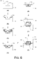
- FIG. 6 is a graphical flow diagram illustrating an example process 600 of forming a microelectronic assembly 300 comprising a pair of substrates 102 and 104 with embedded conductive structures 106 and 108 and one or more barrier interfaces 302, according to an embodiment.
- the method includes forming a cavity 602 (or a plurality of cavities 602 and 603) in a surface of the substrate 102.
- the cavities 602 and 603 may be formed by patterned etching, or the like. In an embodiment, one of the cavities 603 may extend to a depth of less than 5% of a depth of the other cavity 602.
- a barrier layer 604 is formed on the surface of the substrate 102 and within the cavity 602.
- the barrier layer 604 may be comprised of silicon nitride, silicon oxynitride, silicon carbide, silicon carbonitride, diamond, boron doped glass or oxide, aluminum oxide, or other suitable material with worse diffusivity properties than silicon oxide, or a combination thereof, for instance.
- the barrier layer 604 may comprise a conductive material, for example titanium or tantalum or their corresponding nitrides, nickel and nickel alloys, or other conductive materials and combinations.
- the cavity 602 coated with the barrier layer 604 is filled with the conductive material 202, such as copper, a copper alloy, or the like. This could be done using a duel damascene process, for instance. In some examples it may be desirable for the conductive structure 106 to contact the bottom of the cavity 602, at the substrate 102 rather than the barrier layer 604. In these examples, portions of the barrier layer 604 may be removed from the bottom portion (and/or any other desired portion) of the cavity 602 to expose the substrate 102 prior to filling the cavity 602 with the conductive material 202.
- overflow conductive material 202 is removed, by etching, CMP, or the like, stopping at the barrier layer 604, to form a conductive structure 106 (or multiple conductive structures 106) within the barrier layer 604.
- the conductive structure 106 and part of the barrier layer 604 are planarized via CMP, for example, to form a barrier interface 302 partly or fully surrounding an interconnect pad 204, which may have a very small recess, and a substantially planar surface (having a smooth surface topography with a variance of no more than 10-20nm) of the substrate 102.
- the barrier layer 604 or barrier interface 302 is useful to prevent or to mitigate erosion of the insulating material or dielectric of the substrate 102 (e.g., rounding) that can occur during planarization.
- the barrier layer 604 may extend a predetermined extent (i.e., width, diameter, etc.) beyond the conductive structure 106 and over the surface of the substrate 102, protecting the surface of the substrate 102 during planarization.
- the first barrier interface 302 is disposed over at least a portion of the substantially planar surface of the first substrate 102, and is arranged to protect the substantially planar surface from erosion due to planarization or polishing of the substantially planar surface.
- the barrier interface 302 With the barrier interface 302 in place, no dielectric erosion (e.g., rounding) may occur at the intersection of the conductive structure 106 and the substrate 102, or at the intersection of the barrier interface 302 and the substrate 102.
- the barrier interface 302 may be used as an indicator for polishing the substrate 102, and in some examples the barrier interface 302 may be polished a desired amount as well to achieve a flat, smooth bonding surface.
- a like microelectronic structure, with prepared substrate 104, conductive structure 108, and barrier layer 302 is placed onto the substrate 102 for bonding.
- the substrate 104 is direct bonded to the substrate 102 without an intervening material, such as adhesive, to form the microelectronic assembly 300.
- the substrate 104 is bonded to the bonding surface of the substrate 102 and to the barrier layer 302 on the substrate 102, and the substrate 102 is bonded to the bonding surface of the substrate 104 and to the barrier layer 302 on the substrate 104.
- the conductive structures 106 from the substrate 102 and the conductive structures 108 from the substrate 104 can be slightly recessed below the bond-line 110 due to CMP process and may not be in physical contact.
- the conductive structure 108 may be bonded to the conductive structure 106 via heated annealing, or the like. After annealing at high temperature as discussed earlier, the conductive structure 108 is mated to the conductive structure 106 to form electrical connectivity.
- any offset of the conductive structure 106 to the conductive structure 108 due to misalignment rests on the barrier interface 302 rather than on the substrates 102 and 104. Accordingly, diffusion of conductive material (e.g., copper) into substrate 102 and/or 104 material (e.g., silicon oxide) is reduced or eliminated due to the barrier interface(s) 302.
- conductive material e.g., copper
- substrate 102 and/or 104 material e.g., silicon oxide
- an additional layer typically of the same type of material as the substrate 102, e.g. silicon oxide, is deposited over the interconnect pad 204 and the barrier layer 302.
- another planarization process e.g. CMP
- CMP another planarization process
- the barrier layer 302 partially or fully surrounds the interconnect 204 and the substrate layer 102 fully or partially surrounds the barrier layer 302.
- the direct bonding of the bonding layers of 102 and 104 occurs along with the direct bonding of the barrier layer 302 of the substrate 102 with the barrier layer 302 of the substrate 104.
- the annealing step wherein the conductive structure 108 may be bonded to the conductive structure 106 via heated annealing, or the like.
- FIG. 7 is a graphical flow diagram illustrating an example process 700 of forming a microelectronic assembly 300 comprising a pair of substrates 102 and 104 with embedded conductive structures 106 and 108 and one or more barrier interfaces 302, according to another embodiment.
- the method includes depositing the barrier layer material 604 onto the surface of an oxide or other dielectric (for example) substrate 102.
- a portion of the barrier layer 604 and a portion of the dielectric of the substrate 102 are removed, and the resulting cavity 602 is filled with a conductive material 202 (at block C).
- the process of forming the conductive material 202 in the cavity 602 may include coating a second barrier (not shown) over the surface of the first barrier layer 604 and the cavity 602 before filling the cavity 602 with the conductive material 202.
- a conductive structure 106 with interconnect pad 204 surrounded by a barrier interface 302 is formed by planarizing the conductive material 202, and the second barrier layer if present.
- the barrier interface 302 is efficacious to prevent dielectric erosion of the substrate 102 at the intersection of the conductive structure 106 during the planarizing.
- this structure 102 with prepared barrier interface 302 and conductive structure 106 may be bonded to another like structure, but without the barrier interface 302 on the other structure.
- the barrier layer 302 can act as a bonding surface for the other structure, based on the material used for the barrier layer (e.g., silicon nitride, or the like).
- the barrier interface 302 can be altered to remove any unwanted portions.
- a resist, mask, or other pattern 702 may be deposited, and the barrier interface 302 etched as desired (at block F).
- Additional substrate material such as silicon oxide, for example
- the added material may be deposited while the mask 702 is still in place, or after removing the mask 702.
- the surface of the substrate 102 is then planarized (via CMP, or the like) to achieve a flat, smooth surface including the surface of the substrate 102 flush with the barrier interface 302, in preparation for bonding.
- a prepared substrate 102 is shown with an interconnect pad 204 having a partially or fully encompassing barrier interface 302.
- Two similarly prepared substrates 102 and 104 may be stacked and bonded at their planarized surfaces to form a microelectronic structure 300, as shown at block H. Any overlap of conductive material occurs at the barrier interface(s) 302 rather than at the dielectric of the substrates 102 and/or 104.
- This method can also be used to form multiple conductive interconnect structures 106, 108 with barrier interface(s) 302 partially or fully surrounding the multiple conductive interconnect structures 106, 108.
- the conductive structures 106 and/or 108 may include conductive mechanical pads.
- the mechanical pads mate intimately with the barrier layer 302 or the substrate 102/104 to secure the mechanical pads to the substrate 102/104.
- FIG. 8 is a flow diagram describing an example process 800 of forming a microelectronic assembly (such as the microelectronic assembly 300) comprising a pair of substrates (such as the pair of substrates 102 and 104) with embedded conductive structures (such as conductive structures 106 and 108) and one or more barrier interfaces (such as barrier interface 302), according to an embodiment.
- a microelectronic assembly such as the microelectronic assembly 300
- a pair of substrates such as the pair of substrates 102 and 104
- embedded conductive structures such as conductive structures 106 and 10
- barrier interfaces such as barrier interface 302
- the process includes forming a first cavity (or a plurality of first cavities) in a surface of a first substrate (such as substrate 102, for example).
- the first substrate comprises an insulating material or dielectric, such as silicon oxide, or the like, which may be provided on a semiconductor base having circuitry on, in, through the base.
- the process includes forming a first barrier interface (such as barrier interface 302, for example) at the first substrate and at least partially surrounding a perimeter of the first cavity.
- the process includes depositing a first barrier layer material onto at least a portion of a surface of the first cavity.
- the first barrier layer material may also be deposited onto at least a portion of the surface of the first substrate, particularly, partially or fully surrounding the first cavity.
- the first barrier interface comprises a material different from the insulating material or dielectric and is arranged to inhibit a diffusion of a conductive material into the first substrate.
- the process includes filling the first cavity with the conductive material.
- the conductive material comprises copper, a copper alloy, or like conductive material.
- the process includes planarizing at least a portion of the surface of the first substrate, the first barrier interface (including the first barrier layer material), and the conductive material to form a first conductive interconnect structure with a first barrier interface at least partially surrounding an exposed surface of the first conductive interconnect structure.
- the first barrier interface is formed to have a predetermined width.
- the process includes depositing an additional layer of insulating material or dielectric (e.g., silicon oxide) onto the surface of the first substrate to improve the bonding surface of the substrate.
- the depositing may be used to fill any voids created during previous planarization steps, to flush the surface of the substrate with the barrier interface, or the like.
- the surface of the substrate is re-planarized after the depositing to form a flat, smooth, and flush bonding surface.
- the first barrier interface surrounds (at least partially) the conductive interconnect, and the insulating material or dielectric surrounds (at least partially) the first barrier interface.
- the process includes forming a second cavity in a surface of a second substrate (such as substrate 104, for example), where the second substrate also comprises an insulating material or dielectric.
- the process includes forming a second barrier interface at the second substrate and at least partially surrounding a perimeter of the second cavity, where the second barrier interface comprises a material different from the insulating material or dielectric of the second substrate.
- the process includes depositing a second barrier layer material onto at least a portion of the surface of the second substrate and onto at least a portion of a surface of the second cavity.
- the second barrier interface is arranged to inhibit a diffusion of the conductive material of the first conductive structure (embedded in the first substrate) into the second substrate.
- the process includes forming the first barrier interface and/or the second barrier interface to comprise a gas-filled gap.
- the process includes forming the first barrier interface and/or the second barrier interface to comprise a roughened area of the surface of the first substrate and/or the second substrate that inhibits bonding at the roughened area.
- the first barrier interface and/or the second barrier interface comprises one or more of silicon nitride, silicon oxynitride, silicon carbide, silicon carbonitride, diamond, boron doped glass or oxide, aluminum oxide, or a like diffusion resistant material.
- the process includes filling the second cavity with the conductive material and planarizing at least a portion of the surface of the second substrate, the second barrier interface, and the conductive material at the second substrate to form a second conductive interconnect structure (such as the conductive structure 108, for example) with a second barrier interface at least partly surrounding an exposed surface of the second conductive interconnect structure.
- the process includes forming the first barrier interface or the second barrier interface to have a width that is at least 10% of a diameter of the second conductive interconnect structure.
- the process includes forming the first barrier interface or the second barrier interface to have a width that is at least 20% of a diameter/width of the second conductive interconnect structure.
- the process further includes directly bonding the surface of the second substrate to the surface of the first substrate without an adhesive material and mating the second conductive interconnect structure to the first conductive interconnect structure, such that any portion of the second conductive interconnect structure contacts the first barrier interface and not the first substrate and any portion of the first conductive interconnect structure contacts the second barrier interface and not the second substrate when the second conductive interconnect structure and the first conductive interconnect structure are offset or misaligned.
- the process includes directly bonding the exposed surface of the second conductive interconnect structure to the exposed surface of the first conductive interconnect structure.
- the process includes high temperature annealing to bond the conductive structures into a single conductive interconnect.
Landscapes
- Internal Circuitry In Semiconductor Integrated Circuit Devices (AREA)
- Engineering & Computer Science (AREA)
- Manufacturing & Machinery (AREA)
- Non-Metallic Protective Coatings For Printed Circuits (AREA)
- Combinations Of Printed Boards (AREA)
Priority Applications (2)
| Application Number | Priority Date | Filing Date | Title |
|---|---|---|---|
| EP25227107.7A EP4727326A2 (fr) | 2017-10-06 | 2018-10-01 | Collier barrière de diffusion pour interconnexions |
| EP25227115.0A EP4712756A2 (fr) | 2017-10-06 | 2018-10-01 | Collier barrière de diffusion pour interconnexions |
Applications Claiming Priority (4)
| Application Number | Priority Date | Filing Date | Title |
|---|---|---|---|
| US201762569232P | 2017-10-06 | 2017-10-06 | |
| US16/143,850 US11031285B2 (en) | 2017-10-06 | 2018-09-27 | Diffusion barrier collar for interconnects |
| EP18864135.1A EP3692568A4 (fr) | 2017-10-06 | 2018-10-01 | Collier de barrière de diffusion servant à des interconnexions |
| PCT/US2018/053736 WO2019070571A1 (fr) | 2017-10-06 | 2018-10-01 | Collier de barrière de diffusion servant à des interconnexions |
Related Parent Applications (1)
| Application Number | Title | Priority Date | Filing Date |
|---|---|---|---|
| EP18864135.1A Division EP3692568A4 (fr) | 2017-10-06 | 2018-10-01 | Collier de barrière de diffusion servant à des interconnexions |
Related Child Applications (2)
| Application Number | Title | Priority Date | Filing Date |
|---|---|---|---|
| EP25227115.0A Division EP4712756A2 (fr) | 2017-10-06 | 2018-10-01 | Collier barrière de diffusion pour interconnexions |
| EP25227107.7A Division EP4727326A2 (fr) | 2017-10-06 | 2018-10-01 | Collier barrière de diffusion pour interconnexions |
Publications (2)
| Publication Number | Publication Date |
|---|---|
| EP4044229A2 true EP4044229A2 (fr) | 2022-08-17 |
| EP4044229A3 EP4044229A3 (fr) | 2022-11-30 |
Family
ID=65994065
Family Applications (4)
| Application Number | Title | Priority Date | Filing Date |
|---|---|---|---|
| EP25227107.7A Pending EP4727326A2 (fr) | 2017-10-06 | 2018-10-01 | Collier barrière de diffusion pour interconnexions |
| EP25227115.0A Pending EP4712756A2 (fr) | 2017-10-06 | 2018-10-01 | Collier barrière de diffusion pour interconnexions |
| EP18864135.1A Withdrawn EP3692568A4 (fr) | 2017-10-06 | 2018-10-01 | Collier de barrière de diffusion servant à des interconnexions |
| EP22166588.8A Pending EP4044229A3 (fr) | 2017-10-06 | 2018-10-01 | Collier de barrière de diffusion pour interconnexions |
Family Applications Before (3)
| Application Number | Title | Priority Date | Filing Date |
|---|---|---|---|
| EP25227107.7A Pending EP4727326A2 (fr) | 2017-10-06 | 2018-10-01 | Collier barrière de diffusion pour interconnexions |
| EP25227115.0A Pending EP4712756A2 (fr) | 2017-10-06 | 2018-10-01 | Collier barrière de diffusion pour interconnexions |
| EP18864135.1A Withdrawn EP3692568A4 (fr) | 2017-10-06 | 2018-10-01 | Collier de barrière de diffusion servant à des interconnexions |
Country Status (6)
| Country | Link |
|---|---|
| US (5) | US11031285B2 (fr) |
| EP (4) | EP4727326A2 (fr) |
| KR (2) | KR102609290B1 (fr) |
| CN (3) | CN118213350A (fr) |
| TW (1) | TWI756476B (fr) |
| WO (1) | WO2019070571A1 (fr) |
Families Citing this family (115)
| Publication number | Priority date | Publication date | Assignee | Title |
|---|---|---|---|---|
| US7109092B2 (en) | 2003-05-19 | 2006-09-19 | Ziptronix, Inc. | Method of room temperature covalent bonding |
| US7485968B2 (en) | 2005-08-11 | 2009-02-03 | Ziptronix, Inc. | 3D IC method and device |
| US8735219B2 (en) | 2012-08-30 | 2014-05-27 | Ziptronix, Inc. | Heterogeneous annealing method and device |
| US10886250B2 (en) | 2015-07-10 | 2021-01-05 | Invensas Corporation | Structures and methods for low temperature bonding using nanoparticles |
| US9953941B2 (en) | 2015-08-25 | 2018-04-24 | Invensas Bonding Technologies, Inc. | Conductive barrier direct hybrid bonding |
| US10204893B2 (en) | 2016-05-19 | 2019-02-12 | Invensas Bonding Technologies, Inc. | Stacked dies and methods for forming bonded structures |
| US10580735B2 (en) | 2016-10-07 | 2020-03-03 | Xcelsis Corporation | Stacked IC structure with system level wiring on multiple sides of the IC die |
| US10672663B2 (en) | 2016-10-07 | 2020-06-02 | Xcelsis Corporation | 3D chip sharing power circuit |
| US10607136B2 (en) | 2017-08-03 | 2020-03-31 | Xcelsis Corporation | Time borrowing between layers of a three dimensional chip stack |
| TWI822659B (zh) | 2016-10-27 | 2023-11-21 | 美商艾德亞半導體科技有限責任公司 | 用於低溫接合的結構和方法 |
| US10002844B1 (en) | 2016-12-21 | 2018-06-19 | Invensas Bonding Technologies, Inc. | Bonded structures |
| US20180182665A1 (en) | 2016-12-28 | 2018-06-28 | Invensas Bonding Technologies, Inc. | Processed Substrate |
| WO2018125673A2 (fr) | 2016-12-28 | 2018-07-05 | Invensas Bonding Technologies, Inc | Traitement de substrats empilés |
| TWI837879B (zh) | 2016-12-29 | 2024-04-01 | 美商艾德亞半導體接合科技有限公司 | 具有整合式被動構件的接合結構 |
| US10629577B2 (en) | 2017-03-16 | 2020-04-21 | Invensas Corporation | Direct-bonded LED arrays and applications |
| US10515913B2 (en) | 2017-03-17 | 2019-12-24 | Invensas Bonding Technologies, Inc. | Multi-metal contact structure |
| US10508030B2 (en) | 2017-03-21 | 2019-12-17 | Invensas Bonding Technologies, Inc. | Seal for microelectronic assembly |
| US10269756B2 (en) | 2017-04-21 | 2019-04-23 | Invensas Bonding Technologies, Inc. | Die processing |
| US10879212B2 (en) | 2017-05-11 | 2020-12-29 | Invensas Bonding Technologies, Inc. | Processed stacked dies |
| US10446441B2 (en) | 2017-06-05 | 2019-10-15 | Invensas Corporation | Flat metal features for microelectronics applications |
| US10217720B2 (en) | 2017-06-15 | 2019-02-26 | Invensas Corporation | Multi-chip modules formed using wafer-level processing of a reconstitute wafer |
| US10840205B2 (en) * | 2017-09-24 | 2020-11-17 | Invensas Bonding Technologies, Inc. | Chemical mechanical polishing for hybrid bonding |
| US11031285B2 (en) | 2017-10-06 | 2021-06-08 | Invensas Bonding Technologies, Inc. | Diffusion barrier collar for interconnects |
| US11011503B2 (en) | 2017-12-15 | 2021-05-18 | Invensas Bonding Technologies, Inc. | Direct-bonded optoelectronic interconnect for high-density integrated photonics |
| US10923408B2 (en) | 2017-12-22 | 2021-02-16 | Invensas Bonding Technologies, Inc. | Cavity packages |
| US11380597B2 (en) | 2017-12-22 | 2022-07-05 | Invensas Bonding Technologies, Inc. | Bonded structures |
| JP2019140178A (ja) * | 2018-02-07 | 2019-08-22 | 東芝メモリ株式会社 | 半導体装置 |
| US10727219B2 (en) | 2018-02-15 | 2020-07-28 | Invensas Bonding Technologies, Inc. | Techniques for processing devices |
| US11169326B2 (en) | 2018-02-26 | 2021-11-09 | Invensas Bonding Technologies, Inc. | Integrated optical waveguides, direct-bonded waveguide interface joints, optical routing and interconnects |
| US11256004B2 (en) | 2018-03-20 | 2022-02-22 | Invensas Bonding Technologies, Inc. | Direct-bonded lamination for improved image clarity in optical devices |
| US10991804B2 (en) | 2018-03-29 | 2021-04-27 | Xcelsis Corporation | Transistor level interconnection methodologies utilizing 3D interconnects |
| US11056348B2 (en) | 2018-04-05 | 2021-07-06 | Invensas Bonding Technologies, Inc. | Bonding surfaces for microelectronics |
| US10790262B2 (en) | 2018-04-11 | 2020-09-29 | Invensas Bonding Technologies, Inc. | Low temperature bonded structures |
| US11244916B2 (en) | 2018-04-11 | 2022-02-08 | Invensas Bonding Technologies, Inc. | Low temperature bonded structures |
| US10964664B2 (en) | 2018-04-20 | 2021-03-30 | Invensas Bonding Technologies, Inc. | DBI to Si bonding for simplified handle wafer |
| US11004757B2 (en) | 2018-05-14 | 2021-05-11 | Invensas Bonding Technologies, Inc. | Bonded structures |
| US11276676B2 (en) | 2018-05-15 | 2022-03-15 | Invensas Bonding Technologies, Inc. | Stacked devices and methods of fabrication |
| US10923413B2 (en) | 2018-05-30 | 2021-02-16 | Xcelsis Corporation | Hard IP blocks with physically bidirectional passageways |
| US11393779B2 (en) | 2018-06-13 | 2022-07-19 | Invensas Bonding Technologies, Inc. | Large metal pads over TSV |
| WO2019241417A1 (fr) | 2018-06-13 | 2019-12-19 | Invensas Bonding Technologies, Inc. | Tsv en tant que pastille de connexion |
| US10910344B2 (en) | 2018-06-22 | 2021-02-02 | Xcelsis Corporation | Systems and methods for releveled bump planes for chiplets |
| US11664357B2 (en) | 2018-07-03 | 2023-05-30 | Adeia Semiconductor Bonding Technologies Inc. | Techniques for joining dissimilar materials in microelectronics |
| WO2020010265A1 (fr) | 2018-07-06 | 2020-01-09 | Invensas Bonding Technologies, Inc. | Ensembles microélectroniques |
| WO2020010136A1 (fr) | 2018-07-06 | 2020-01-09 | Invensas Bonding Technologies, Inc. | Empilement moulé interconnecté et lié directement |
| US12406959B2 (en) | 2018-07-26 | 2025-09-02 | Adeia Semiconductor Bonding Technologies Inc. | Post CMP processing for hybrid bonding |
| US11515291B2 (en) | 2018-08-28 | 2022-11-29 | Adeia Semiconductor Inc. | Integrated voltage regulator and passive components |
| US11296044B2 (en) | 2018-08-29 | 2022-04-05 | Invensas Bonding Technologies, Inc. | Bond enhancement structure in microelectronics for trapping contaminants during direct-bonding processes |
| US11011494B2 (en) | 2018-08-31 | 2021-05-18 | Invensas Bonding Technologies, Inc. | Layer structures for making direct metal-to-metal bonds at low temperatures in microelectronics |
| US11158573B2 (en) | 2018-10-22 | 2021-10-26 | Invensas Bonding Technologies, Inc. | Interconnect structures |
| KR102518803B1 (ko) * | 2018-10-24 | 2023-04-07 | 삼성전자주식회사 | 반도체 패키지 |
| US11244920B2 (en) | 2018-12-18 | 2022-02-08 | Invensas Bonding Technologies, Inc. | Method and structures for low temperature device bonding |
| KR20210104742A (ko) | 2019-01-14 | 2021-08-25 | 인벤사스 본딩 테크놀로지스 인코포레이티드 | 접합 구조체 |
| US11387202B2 (en) | 2019-03-01 | 2022-07-12 | Invensas Llc | Nanowire bonding interconnect for fine-pitch microelectronics |
| US11901281B2 (en) | 2019-03-11 | 2024-02-13 | Adeia Semiconductor Bonding Technologies Inc. | Bonded structures with integrated passive component |
| US10854578B2 (en) | 2019-03-29 | 2020-12-01 | Invensas Corporation | Diffused bitline replacement in stacked wafer memory |
| US11373963B2 (en) | 2019-04-12 | 2022-06-28 | Invensas Bonding Technologies, Inc. | Protective elements for bonded structures |
| US11205625B2 (en) | 2019-04-12 | 2021-12-21 | Invensas Bonding Technologies, Inc. | Wafer-level bonding of obstructive elements |
| US11610846B2 (en) | 2019-04-12 | 2023-03-21 | Adeia Semiconductor Bonding Technologies Inc. | Protective elements for bonded structures including an obstructive element |
| US11355404B2 (en) | 2019-04-22 | 2022-06-07 | Invensas Bonding Technologies, Inc. | Mitigating surface damage of probe pads in preparation for direct bonding of a substrate |
| US11385278B2 (en) | 2019-05-23 | 2022-07-12 | Invensas Bonding Technologies, Inc. | Security circuitry for bonded structures |
| US12374641B2 (en) | 2019-06-12 | 2025-07-29 | Adeia Semiconductor Bonding Technologies Inc. | Sealed bonded structures and methods for forming the same |
| US11296053B2 (en) | 2019-06-26 | 2022-04-05 | Invensas Bonding Technologies, Inc. | Direct bonded stack structures for increased reliability and improved yield in microelectronics |
| KR102780353B1 (ko) | 2019-08-26 | 2025-03-12 | 삼성전자주식회사 | 반도체 장치 및 그 제조방법 |
| JP7421292B2 (ja) * | 2019-09-11 | 2024-01-24 | キオクシア株式会社 | 半導体装置の製造方法 |
| US12080672B2 (en) | 2019-09-26 | 2024-09-03 | Adeia Semiconductor Bonding Technologies Inc. | Direct gang bonding methods including directly bonding first element to second element to form bonded structure without adhesive |
| US11404307B2 (en) * | 2019-09-27 | 2022-08-02 | Intel Corporation | Interconnect structures and methods of fabrication |
| US12113054B2 (en) | 2019-10-21 | 2024-10-08 | Adeia Semiconductor Technologies Llc | Non-volatile dynamic random access memory |
| KR102740759B1 (ko) | 2019-10-23 | 2024-12-12 | 삼성전자주식회사 | 반도체 패키지 |
| US11862602B2 (en) | 2019-11-07 | 2024-01-02 | Adeia Semiconductor Technologies Llc | Scalable architecture for reduced cycles across SOC |
| US11762200B2 (en) | 2019-12-17 | 2023-09-19 | Adeia Semiconductor Bonding Technologies Inc. | Bonded optical devices |
| US11876076B2 (en) | 2019-12-20 | 2024-01-16 | Adeia Semiconductor Technologies Llc | Apparatus for non-volatile random access memory stacks |
| US11721653B2 (en) | 2019-12-23 | 2023-08-08 | Adeia Semiconductor Bonding Technologies Inc. | Circuitry for electrical redundancy in bonded structures |
| CN121793755A (zh) | 2019-12-23 | 2026-04-03 | 隔热半导体粘合技术公司 | 用于接合结构的电冗余 |
| US11088076B2 (en) * | 2019-12-27 | 2021-08-10 | Sandisk Technologies Llc | Bonding pads embedded in a dielectric diffusion barrier and having recessed metallic liners |
| JP2022528073A (ja) | 2020-02-17 | 2022-06-08 | 長江存儲科技有限責任公司 | ハイブリッドウェハ接合方法およびその構造 |
| CN115943489A (zh) | 2020-03-19 | 2023-04-07 | 隔热半导体粘合技术公司 | 用于直接键合结构的尺寸补偿控制 |
| US11742314B2 (en) | 2020-03-31 | 2023-08-29 | Adeia Semiconductor Bonding Technologies Inc. | Reliable hybrid bonded apparatus |
| US11735523B2 (en) | 2020-05-19 | 2023-08-22 | Adeia Semiconductor Bonding Technologies Inc. | Laterally unconfined structure |
| US11631647B2 (en) | 2020-06-30 | 2023-04-18 | Adeia Semiconductor Bonding Technologies Inc. | Integrated device packages with integrated device die and dummy element |
| US11764177B2 (en) | 2020-09-04 | 2023-09-19 | Adeia Semiconductor Bonding Technologies Inc. | Bonded structure with interconnect structure |
| US11728273B2 (en) | 2020-09-04 | 2023-08-15 | Adeia Semiconductor Bonding Technologies Inc. | Bonded structure with interconnect structure |
| US11990448B2 (en) | 2020-09-18 | 2024-05-21 | Intel Corporation | Direct bonding in microelectronic assemblies |
| US12199018B2 (en) * | 2020-09-18 | 2025-01-14 | Intel Corporation | Direct bonding in microelectronic assemblies |
| US11264357B1 (en) | 2020-10-20 | 2022-03-01 | Invensas Corporation | Mixed exposure for large die |
| KR20230097121A (ko) * | 2020-10-29 | 2023-06-30 | 아데이아 세미컨덕터 본딩 테크놀로지스 인코포레이티드 | 직접 접합 방법 및 구조체 |
| WO2022147430A1 (fr) | 2020-12-28 | 2022-07-07 | Invensas Bonding Technologies, Inc. | Structures comprenant des trous d'interconnexion traversant un substrat et leurs procédés de formation |
| US12456662B2 (en) | 2020-12-28 | 2025-10-28 | Adeia Semiconductor Bonding Technologies Inc. | Structures with through-substrate vias and methods for forming the same |
| CN116848631A (zh) | 2020-12-30 | 2023-10-03 | 美商艾德亚半导体接合科技有限公司 | 具有导电特征的结构及其形成方法 |
| US20220208723A1 (en) * | 2020-12-30 | 2022-06-30 | Invensas Bonding Technologies, Inc. | Directly bonded structures |
| CN114743942B (zh) * | 2021-01-07 | 2026-02-10 | 联华电子股份有限公司 | 混合式接合结构及其制作方法 |
| EP4315411A4 (fr) | 2021-03-31 | 2025-04-30 | Adeia Semiconductor Bonding Technologies Inc. | Procédés et structures de liaison directe |
| US12525572B2 (en) | 2021-03-31 | 2026-01-13 | Adeia Semiconductor Bonding Technologies Inc. | Direct bonding and debonding of carrier |
| US11587895B2 (en) * | 2021-04-21 | 2023-02-21 | Micron Technology, Inc. | Semiconductor interconnect structures with vertically offset bonding surfaces, and associated systems and methods |
| KR20220168234A (ko) | 2021-06-15 | 2022-12-23 | 삼성전자주식회사 | 반도체 패키지 |
| CN115565978B (zh) * | 2021-07-01 | 2024-09-27 | 长鑫存储技术有限公司 | 半导体结构及半导体结构的制作方法 |
| JP7583173B2 (ja) * | 2021-07-01 | 2024-11-13 | チャンシン メモリー テクノロジーズ インコーポレイテッド | 半導体構造及び半導体構造の製造方法 |
| JP2024528964A (ja) | 2021-08-02 | 2024-08-01 | アデイア セミコンダクター ボンディング テクノロジーズ インコーポレイテッド | ボンデッド構造体用の保護半導体素子 |
| KR20240059637A (ko) | 2021-09-24 | 2024-05-07 | 아데이아 세미컨덕터 본딩 테크놀로지스 인코포레이티드 | 능동 인터포저를 가진 결합 구조체 |
| US12604771B2 (en) | 2021-10-28 | 2026-04-14 | Adeia Semiconductor Bonding Technologies Inc. | Direct bonding methods and structures |
| US12563749B2 (en) | 2021-10-28 | 2026-02-24 | Adeia Semiconductor Bonding Technologies Inc | Stacked electronic devices |
| EP4423806A4 (fr) * | 2021-10-28 | 2025-09-24 | Adeia Semiconductor Bonding Technologies Inc | Barrières de diffusion et procédé de formation associé |
| KR20230068590A (ko) | 2021-11-11 | 2023-05-18 | 삼성전자주식회사 | 반도체 패키지 및 그 제조방법 |
| US12557615B2 (en) | 2021-12-13 | 2026-02-17 | Adeia Semiconductor Technologies Llc | Methods for bonding semiconductor elements |
| JP2025500315A (ja) | 2021-12-20 | 2025-01-09 | アデイア セミコンダクター ボンディング テクノロジーズ インコーポレイテッド | ダイパッケージの熱電冷却 |
| JP2024545315A (ja) * | 2021-12-22 | 2024-12-05 | アデイア セミコンダクター ボンディング テクノロジーズ インコーポレイテッド | 低応力直接ハイブリッド接合 |
| KR20230142082A (ko) | 2022-03-31 | 2023-10-11 | 삼성전자주식회사 | 반도체 장치 및 그의 제조 방법 |
| US12512425B2 (en) | 2022-04-25 | 2025-12-30 | Adeia Semiconductor Bonding Technologies Inc. | Expansion controlled structure for direct bonding and method of forming same |
| JP2025517291A (ja) | 2022-05-23 | 2025-06-05 | アデイア セミコンダクター ボンディング テクノロジーズ インコーポレイテッド | ボンデッド構造体のための試験用素子 |
| KR20240022207A (ko) * | 2022-08-11 | 2024-02-20 | 삼성전자주식회사 | 반도체 패키지 및 그 제조 방법 |
| US12444672B2 (en) * | 2022-09-30 | 2025-10-14 | Intel Corporation | Hybrid bonding technologies with thermal expansion compensation structures |
| US12506114B2 (en) | 2022-12-29 | 2025-12-23 | Adeia Semiconductor Bonding Technologies Inc. | Directly bonded metal structures having aluminum features and methods of preparing same |
| US12545010B2 (en) | 2022-12-29 | 2026-02-10 | Adeia Semiconductor Bonding Technologies Inc. | Directly bonded metal structures having oxide layers therein |
| US12341083B2 (en) | 2023-02-08 | 2025-06-24 | Adeia Semiconductor Bonding Technologies Inc. | Electronic device cooling structures bonded to semiconductor elements |
| US12598962B2 (en) | 2023-03-14 | 2026-04-07 | Adeia Semiconductor Bonding Technologies Inc. | System and method for bonding transparent conductor substrates |
| US20240387426A1 (en) * | 2023-05-18 | 2024-11-21 | International Business Machines Corporation | Electromigration resistant semiconductor structure |
Citations (2)
| Publication number | Priority date | Publication date | Assignee | Title |
|---|---|---|---|---|
| US6864585B2 (en) | 2000-03-22 | 2005-03-08 | Ziptronix, Inc. | Three dimensional device integration method and integrated device |
| US7485968B2 (en) | 2005-08-11 | 2009-02-03 | Ziptronix, Inc. | 3D IC method and device |
Family Cites Families (277)
| Publication number | Priority date | Publication date | Assignee | Title |
|---|---|---|---|---|
| JPH0629718A (ja) * | 1992-07-06 | 1994-02-04 | Nippon Telegr & Teleph Corp <Ntt> | アンテナの方位設定方法 |
| JPH07193294A (ja) | 1993-11-01 | 1995-07-28 | Matsushita Electric Ind Co Ltd | 電子部品およびその製造方法 |
| KR960009074A (ko) | 1994-08-29 | 1996-03-22 | 모리시다 요이치 | 반도체 장치 및 그 제조방법 |
| US5755859A (en) | 1995-08-24 | 1998-05-26 | International Business Machines Corporation | Cobalt-tin alloys and their applications for devices, chip interconnections and packaging |
| US6097096A (en) | 1997-07-11 | 2000-08-01 | Advanced Micro Devices | Metal attachment method and structure for attaching substrates at low temperatures |
| JP3532788B2 (ja) | 1999-04-13 | 2004-05-31 | 唯知 須賀 | 半導体装置及びその製造方法 |
| US6984571B1 (en) | 1999-10-01 | 2006-01-10 | Ziptronix, Inc. | Three dimensional device integration method and integrated device |
| US6902987B1 (en) | 2000-02-16 | 2005-06-07 | Ziptronix, Inc. | Method for low temperature bonding and bonded structure |
| US6423640B1 (en) | 2000-08-09 | 2002-07-23 | Taiwan Semiconductor Manufacturing Co., Ltd. | Headless CMP process for oxide planarization |
| US6887769B2 (en) | 2002-02-06 | 2005-05-03 | Intel Corporation | Dielectric recess for wafer-to-wafer and die-to-die metal bonding and method of fabricating the same |
| US6762076B2 (en) | 2002-02-20 | 2004-07-13 | Intel Corporation | Process of vertically stacking multiple wafers supporting different active integrated circuit (IC) devices |
| US6693356B2 (en) | 2002-03-27 | 2004-02-17 | Texas Instruments Incorporated | Copper transition layer for improving copper interconnection reliability |
| US7105980B2 (en) | 2002-07-03 | 2006-09-12 | Sawtek, Inc. | Saw filter device and method employing normal temperature bonding for producing desirable filter production and performance characteristics |
| JP4083502B2 (ja) | 2002-08-19 | 2008-04-30 | 株式会社フジミインコーポレーテッド | 研磨方法及びそれに用いられる研磨用組成物 |
| US7023093B2 (en) | 2002-10-24 | 2006-04-04 | International Business Machines Corporation | Very low effective dielectric constant interconnect Structures and methods for fabricating the same |
| US6962835B2 (en) | 2003-02-07 | 2005-11-08 | Ziptronix, Inc. | Method for room temperature metal direct bonding |
| US6908027B2 (en) | 2003-03-31 | 2005-06-21 | Intel Corporation | Complete device layer transfer without edge exclusion via direct wafer bonding and constrained bond-strengthening process |
| US7109092B2 (en) | 2003-05-19 | 2006-09-19 | Ziptronix, Inc. | Method of room temperature covalent bonding |
| US6867073B1 (en) | 2003-10-21 | 2005-03-15 | Ziptronix, Inc. | Single mask via method and device |
| DE102004021239B4 (de) * | 2004-04-30 | 2017-04-06 | Infineon Technologies Ag | Lange getemperte integrierte Schaltungsanordnungen und deren Herstellungsverfahren |
| US20060057945A1 (en) | 2004-09-16 | 2006-03-16 | Chia-Lin Hsu | Chemical mechanical polishing process |
| US7193423B1 (en) | 2005-12-12 | 2007-03-20 | International Business Machines Corporation | Wafer-to-wafer alignments |
| US7750488B2 (en) | 2006-07-10 | 2010-07-06 | Tezzaron Semiconductor, Inc. | Method for bonding wafers to produce stacked integrated circuits |
| US7902643B2 (en) * | 2006-08-31 | 2011-03-08 | Micron Technology, Inc. | Microfeature workpieces having interconnects and conductive backplanes, and associated systems and methods |
| US7964496B2 (en) | 2006-11-21 | 2011-06-21 | Taiwan Semiconductor Manufacturing Company, Ltd. | Schemes for forming barrier layers for copper in interconnect structures |
| US7803693B2 (en) | 2007-02-15 | 2010-09-28 | John Trezza | Bowed wafer hybridization compensation |
| US8349635B1 (en) | 2008-05-20 | 2013-01-08 | Silicon Laboratories Inc. | Encapsulated MEMS device and method to form the same |
| US9893004B2 (en) | 2011-07-27 | 2018-02-13 | Broadpak Corporation | Semiconductor interposer integration |
| US7855455B2 (en) * | 2008-09-26 | 2010-12-21 | International Business Machines Corporation | Lock and key through-via method for wafer level 3 D integration and structures produced |
| US8049336B2 (en) | 2008-09-30 | 2011-11-01 | Infineon Technologies, Ag | Interconnect structure |
| JP4415100B1 (ja) | 2008-12-19 | 2010-02-17 | 国立大学法人東北大学 | 銅配線、半導体装置および銅配線形成方法 |
| US8476165B2 (en) | 2009-04-01 | 2013-07-02 | Tokyo Electron Limited | Method for thinning a bonding wafer |
| US8482132B2 (en) | 2009-10-08 | 2013-07-09 | International Business Machines Corporation | Pad bonding employing a self-aligned plated liner for adhesion enhancement |
| WO2011153712A1 (fr) | 2010-06-12 | 2011-12-15 | Theracos, Inc. | Forme cristalline d'inhibiteur de sglt2 de type benzyl-benzène |
| JP5517800B2 (ja) | 2010-07-09 | 2014-06-11 | キヤノン株式会社 | 固体撮像装置用の部材および固体撮像装置の製造方法 |
| GB201012226D0 (en) * | 2010-07-21 | 2010-09-08 | Fujifilm Mfg Europe Bv | Method for manufacturing a barrier on a sheet and a sheet for PV modules |
| FR2966283B1 (fr) | 2010-10-14 | 2012-11-30 | Soi Tec Silicon On Insulator Tech Sa | Procede pour realiser une structure de collage |
| US8377798B2 (en) | 2010-11-10 | 2013-02-19 | Taiwan Semiconductor Manufacturing Co., Ltd | Method and structure for wafer to wafer bonding in semiconductor packaging |
| US8620164B2 (en) | 2011-01-20 | 2013-12-31 | Intel Corporation | Hybrid III-V silicon laser formed by direct bonding |
| CN102615584A (zh) | 2011-01-31 | 2012-08-01 | 中芯国际集成电路制造(上海)有限公司 | 一种化学机械研磨的方法 |
| JP2012164813A (ja) | 2011-02-07 | 2012-08-30 | Toshiba Corp | 半導体装置の製造方法 |
| US8501537B2 (en) | 2011-03-31 | 2013-08-06 | Soitec | Methods for bonding semiconductor structures involving annealing processes, and bonded semiconductor structures formed using such methods |
| US8716105B2 (en) | 2011-03-31 | 2014-05-06 | Soitec | Methods for bonding semiconductor structures involving annealing processes, and bonded semiconductor structures and intermediate structures formed using such methods |
| KR101952976B1 (ko) | 2011-05-24 | 2019-02-27 | 소니 주식회사 | 반도체 장치 |
| US8896125B2 (en) * | 2011-07-05 | 2014-11-25 | Sony Corporation | Semiconductor device, fabrication method for a semiconductor device and electronic apparatus |
| TWI495041B (zh) * | 2011-07-05 | 2015-08-01 | 新力股份有限公司 | 半導體裝置、用於半導體裝置之製造方法及電子設備 |
| JP5982748B2 (ja) | 2011-08-01 | 2016-08-31 | ソニー株式会社 | 半導体装置、半導体装置の製造方法、および電子機器 |
| US8828745B2 (en) | 2011-07-06 | 2014-09-09 | United Microelectronics Corp. | Method for manufacturing through-silicon via |
| US9125333B2 (en) * | 2011-07-15 | 2015-09-01 | Tessera, Inc. | Electrical barrier layers |
| US8697493B2 (en) | 2011-07-18 | 2014-04-15 | Soitec | Bonding surfaces for direct bonding of semiconductor structures |
| US8441131B2 (en) | 2011-09-12 | 2013-05-14 | Globalfoundries Inc. | Strain-compensating fill patterns for controlling semiconductor chip package interactions |
| JP5994274B2 (ja) * | 2012-02-14 | 2016-09-21 | ソニー株式会社 | 半導体装置、半導体装置の製造方法、及び、電子機器 |
| CN103377911B (zh) | 2012-04-16 | 2016-09-21 | 中国科学院微电子研究所 | 提高化学机械平坦化工艺均匀性的方法 |
| US8809123B2 (en) | 2012-06-05 | 2014-08-19 | Taiwan Semiconductor Manufacturing Company, Ltd. | Three dimensional integrated circuit structures and hybrid bonding methods for semiconductor wafers |
| US9142517B2 (en) * | 2012-06-05 | 2015-09-22 | Taiwan Semiconductor Manufacturing Company, Ltd. | Hybrid bonding mechanisms for semiconductor wafers |
| US8710660B2 (en) | 2012-07-20 | 2014-04-29 | Taiwan Semiconductor Manufacturing Company, Ltd. | Hybrid interconnect scheme including aluminum metal line in low-k dielectric |
| US8735219B2 (en) | 2012-08-30 | 2014-05-27 | Ziptronix, Inc. | Heterogeneous annealing method and device |
| US20140175655A1 (en) | 2012-12-22 | 2014-06-26 | Industrial Technology Research Institute | Chip bonding structure and manufacturing method thereof |
| US8946784B2 (en) | 2013-02-18 | 2015-02-03 | Taiwan Semiconductor Manufacturing Company, Ltd. | Method and apparatus for image sensor packaging |
| US9076715B2 (en) | 2013-03-12 | 2015-07-07 | Taiwan Semiconductor Manufacturing Company, Ltd. | Interconnect structure for connecting dies and methods of forming the same |
| US9287197B2 (en) | 2013-03-15 | 2016-03-15 | Globalfoundries Singapore Pte. Ltd. | Through silicon vias |
| US8802538B1 (en) | 2013-03-15 | 2014-08-12 | Taiwan Semiconductor Manufacturing Company, Ltd. | Methods for hybrid wafer bonding |
| US9443796B2 (en) | 2013-03-15 | 2016-09-13 | Taiwan Semiconductor Manufacturing Company, Ltd. | Air trench in packages incorporating hybrid bonding |
| US9064937B2 (en) | 2013-05-30 | 2015-06-23 | International Business Machines Corporation | Substrate bonding with diffusion barrier structures |
| US8860229B1 (en) * | 2013-07-16 | 2014-10-14 | Taiwan Semiconductor Manufacturing Co., Ltd. | Hybrid bonding with through substrate via (TSV) |
| US9929050B2 (en) | 2013-07-16 | 2018-03-27 | Taiwan Semiconductor Manufacturing Company, Ltd. | Mechanisms for forming three-dimensional integrated circuit (3DIC) stacking structure |
| US9723716B2 (en) | 2013-09-27 | 2017-08-01 | Infineon Technologies Ag | Contact pad structure, an electronic component, and a method for manufacturing a contact pad structure |
| US9257399B2 (en) | 2013-10-17 | 2016-02-09 | Taiwan Semiconductor Manufacturing Company, Ltd. | 3D integrated circuit and methods of forming the same |
| JP2015115446A (ja) | 2013-12-11 | 2015-06-22 | 株式会社東芝 | 半導体装置の製造方法 |
| US9437572B2 (en) | 2013-12-18 | 2016-09-06 | Taiwan Semiconductor Manufacturing Company, Ltd. | Conductive pad structure for hybrid bonding and methods of forming same |
| US9412662B2 (en) * | 2014-01-28 | 2016-08-09 | Taiwan Semiconductor Manufacturing Company, Ltd. | Structure and approach to prevent thin wafer crack |
| US9425155B2 (en) * | 2014-02-25 | 2016-08-23 | Taiwan Semiconductor Manufacturing Company, Ltd. | Wafer bonding process and structure |
| US20150262902A1 (en) | 2014-03-12 | 2015-09-17 | Invensas Corporation | Integrated circuits protected by substrates with cavities, and methods of manufacture |
| US9230941B2 (en) | 2014-03-28 | 2016-01-05 | Taiwan Semiconductor Manufacturing Company, Ltd. | Bonding structure for stacked semiconductor devices |
| US9299736B2 (en) | 2014-03-28 | 2016-03-29 | Taiwan Semiconductor Manufacturing Company, Ltd. | Hybrid bonding with uniform pattern density |
| US9472458B2 (en) | 2014-06-04 | 2016-10-18 | Semiconductor Components Industries, Llc | Method of reducing residual contamination in singulated semiconductor die |
| KR102275705B1 (ko) | 2014-07-11 | 2021-07-09 | 삼성전자주식회사 | 웨이퍼 대 웨이퍼 접합 구조 |
| KR20160013756A (ko) * | 2014-07-28 | 2016-02-05 | 에스케이하이닉스 주식회사 | 연결구조물, 반도체 장치 및 그 제조 방법 |
| FR3025051A1 (fr) * | 2014-08-22 | 2016-02-26 | Commissariat Energie Atomique | Procede de realisation d'un circuit integre par collage direct de substrats comprenant en surface des portions de cuivre et de materiau dielectrique |
| US9536848B2 (en) | 2014-10-16 | 2017-01-03 | Globalfoundries Inc. | Bond pad structure for low temperature flip chip bonding |
| US9659856B2 (en) | 2014-10-24 | 2017-05-23 | Taiwan Semiconductor Manufacturing Company, Ltd. | Two step metallization formation |
| KR102211143B1 (ko) * | 2014-11-13 | 2021-02-02 | 삼성전자주식회사 | 반도체 장치 및 그 제조 방법 |
| US9595467B2 (en) * | 2014-11-14 | 2017-03-14 | Applied Materials, Inc. | Air gap formation in interconnection structure by implantation process |
| US9394161B2 (en) | 2014-11-14 | 2016-07-19 | Taiwan Semiconductor Manufacturing Co., Ltd. | MEMS and CMOS integration with low-temperature bonding |
| US10727122B2 (en) * | 2014-12-08 | 2020-07-28 | International Business Machines Corporation | Self-aligned via interconnect structures |
| US11069734B2 (en) | 2014-12-11 | 2021-07-20 | Invensas Corporation | Image sensor device |
| US9972602B2 (en) * | 2015-02-23 | 2018-05-15 | Marvell World Trade Ltd. | Method and apparatus for interconnecting stacked dies using metal posts |
| KR102279757B1 (ko) | 2015-03-06 | 2021-07-21 | 에스케이하이닉스 주식회사 | 확산 방지막의 형성 방법, 상기 확산 방지막을 포함하는 반도체 소자의 금속 배선 및 이의 제조 방법 |
| JP2016181531A (ja) * | 2015-03-23 | 2016-10-13 | ソニー株式会社 | 半導体装置、および半導体装置の製造方法、固体撮像素子、撮像装置、並びに電子機器 |
| JP2016219660A (ja) * | 2015-05-22 | 2016-12-22 | ソニー株式会社 | 半導体装置、製造方法、固体撮像素子、および電子機器 |
| CN106298527B (zh) * | 2015-06-01 | 2019-07-30 | 中芯国际集成电路制造(上海)有限公司 | Pmos晶体管及其形成方法 |
| US9741620B2 (en) | 2015-06-24 | 2017-08-22 | Invensas Corporation | Structures and methods for reliable packages |
| US9656852B2 (en) | 2015-07-06 | 2017-05-23 | Taiwan Semiconductor Manufacturing Company Ltd. | CMOS-MEMS device structure, bonding mesa structure and associated method |
| US10886250B2 (en) | 2015-07-10 | 2021-01-05 | Invensas Corporation | Structures and methods for low temperature bonding using nanoparticles |
| US10075657B2 (en) | 2015-07-21 | 2018-09-11 | Fermi Research Alliance, Llc | Edgeless large area camera system |
| US9728521B2 (en) | 2015-07-23 | 2017-08-08 | Taiwan Semiconductor Manufacturing Co., Ltd. | Hybrid bond using a copper alloy for yield improvement |
| US9559081B1 (en) | 2015-08-21 | 2017-01-31 | Apple Inc. | Independent 3D stacking |
| US9953941B2 (en) | 2015-08-25 | 2018-04-24 | Invensas Bonding Technologies, Inc. | Conductive barrier direct hybrid bonding |
| US9496239B1 (en) | 2015-12-11 | 2016-11-15 | International Business Machines Corporation | Nitride-enriched oxide-to-oxide 3D wafer bonding |
| US9852988B2 (en) | 2015-12-18 | 2017-12-26 | Invensas Bonding Technologies, Inc. | Increased contact alignment tolerance for direct bonding |
| KR20170075125A (ko) * | 2015-12-22 | 2017-07-03 | 에스케이하이닉스 주식회사 | 반도체 패키지 및 제조 방법 |
| US9923011B2 (en) | 2016-01-12 | 2018-03-20 | Taiwan Semiconductor Manufacturing Co., Ltd. | Semiconductor device structure with stacked semiconductor dies |
| US10446532B2 (en) | 2016-01-13 | 2019-10-15 | Invensas Bonding Technologies, Inc. | Systems and methods for efficient transfer of semiconductor elements |
| JP2017135247A (ja) * | 2016-01-27 | 2017-08-03 | 日本放送協会 | 接合型半導体素子、半導体素子、接合型半導体素子の製造方法および半導体素子の製造方法 |
| TWI701782B (zh) * | 2016-01-27 | 2020-08-11 | 美商艾馬克科技公司 | 半導體封裝以及其製造方法 |
| US10026716B2 (en) | 2016-04-15 | 2018-07-17 | Taiwan Semiconductor Manufacturing Company, Ltd. | 3DIC formation with dies bonded to formed RDLs |
| US10204893B2 (en) | 2016-05-19 | 2019-02-12 | Invensas Bonding Technologies, Inc. | Stacked dies and methods for forming bonded structures |
| KR102505856B1 (ko) | 2016-06-09 | 2023-03-03 | 삼성전자 주식회사 | 웨이퍼 대 웨이퍼 접합 구조체 |
| US9780035B1 (en) | 2016-06-30 | 2017-10-03 | International Business Machines Corporation | Structure and method for improved stabilization of cobalt cap and/or cobalt liner in interconnects |
| US9941241B2 (en) | 2016-06-30 | 2018-04-10 | International Business Machines Corporation | Method for wafer-wafer bonding |
| US9892961B1 (en) | 2016-08-09 | 2018-02-13 | International Business Machines Corporation | Air gap spacer formation for nano-scale semiconductor devices |
| US10446487B2 (en) | 2016-09-30 | 2019-10-15 | Invensas Bonding Technologies, Inc. | Interface structures and methods for forming same |
| US10672663B2 (en) | 2016-10-07 | 2020-06-02 | Xcelsis Corporation | 3D chip sharing power circuit |
| US10607136B2 (en) | 2017-08-03 | 2020-03-31 | Xcelsis Corporation | Time borrowing between layers of a three dimensional chip stack |
| US10580735B2 (en) | 2016-10-07 | 2020-03-03 | Xcelsis Corporation | Stacked IC structure with system level wiring on multiple sides of the IC die |
| US10163750B2 (en) | 2016-12-05 | 2018-12-25 | Taiwan Semiconductor Manufacturing Company, Ltd. | Package structure for heat dissipation |
| US10453832B2 (en) | 2016-12-15 | 2019-10-22 | Taiwan Semiconductor Manufacturing Co., Ltd. | Seal ring structures and methods of forming same |
| US10002844B1 (en) | 2016-12-21 | 2018-06-19 | Invensas Bonding Technologies, Inc. | Bonded structures |
| US20180182665A1 (en) | 2016-12-28 | 2018-06-28 | Invensas Bonding Technologies, Inc. | Processed Substrate |
| WO2018125673A2 (fr) | 2016-12-28 | 2018-07-05 | Invensas Bonding Technologies, Inc | Traitement de substrats empilés |
| TWI837879B (zh) | 2016-12-29 | 2024-04-01 | 美商艾德亞半導體接合科技有限公司 | 具有整合式被動構件的接合結構 |
| US20180190583A1 (en) | 2016-12-29 | 2018-07-05 | Invensas Bonding Technologies, Inc. | Bonded structures with integrated passive component |
| US10276909B2 (en) | 2016-12-30 | 2019-04-30 | Invensas Bonding Technologies, Inc. | Structure comprising at least a first element bonded to a carrier having a closed metallic channel waveguide formed therein |
| US10431614B2 (en) | 2017-02-01 | 2019-10-01 | Semiconductor Components Industries, Llc | Edge seals for semiconductor packages |
| JP7030825B2 (ja) | 2017-02-09 | 2022-03-07 | インヴェンサス ボンディング テクノロジーズ インコーポレイテッド | 接合構造物 |
| US10629577B2 (en) | 2017-03-16 | 2020-04-21 | Invensas Corporation | Direct-bonded LED arrays and applications |
| US10515913B2 (en) | 2017-03-17 | 2019-12-24 | Invensas Bonding Technologies, Inc. | Multi-metal contact structure |
| US10508030B2 (en) | 2017-03-21 | 2019-12-17 | Invensas Bonding Technologies, Inc. | Seal for microelectronic assembly |
| JP6640780B2 (ja) | 2017-03-22 | 2020-02-05 | キオクシア株式会社 | 半導体装置の製造方法および半導体装置 |
| WO2018183739A1 (fr) | 2017-03-31 | 2018-10-04 | Invensas Bonding Technologies, Inc. | Structures d'interface et leurs procedes de formation |
| US10269756B2 (en) | 2017-04-21 | 2019-04-23 | Invensas Bonding Technologies, Inc. | Die processing |
| US10580823B2 (en) | 2017-05-03 | 2020-03-03 | United Microelectronics Corp. | Wafer level packaging method |
| US10879212B2 (en) | 2017-05-11 | 2020-12-29 | Invensas Bonding Technologies, Inc. | Processed stacked dies |
| US10446441B2 (en) | 2017-06-05 | 2019-10-15 | Invensas Corporation | Flat metal features for microelectronics applications |
| US10217720B2 (en) | 2017-06-15 | 2019-02-26 | Invensas Corporation | Multi-chip modules formed using wafer-level processing of a reconstitute wafer |
| US10840205B2 (en) | 2017-09-24 | 2020-11-17 | Invensas Bonding Technologies, Inc. | Chemical mechanical polishing for hybrid bonding |
| US11195748B2 (en) | 2017-09-27 | 2021-12-07 | Invensas Corporation | Interconnect structures and methods for forming same |
| US11031285B2 (en) | 2017-10-06 | 2021-06-08 | Invensas Bonding Technologies, Inc. | Diffusion barrier collar for interconnects |
| US10504784B2 (en) | 2017-10-25 | 2019-12-10 | Taiwan Semiconductor Manufacturing Co., Ltd. | Inductor structure for integrated circuit |
| US11251157B2 (en) | 2017-11-01 | 2022-02-15 | Taiwan Semiconductor Manufacturing Company, Ltd. | Die stack structure with hybrid bonding structure and method of fabricating the same and package |
| US11011503B2 (en) | 2017-12-15 | 2021-05-18 | Invensas Bonding Technologies, Inc. | Direct-bonded optoelectronic interconnect for high-density integrated photonics |
| US11380597B2 (en) | 2017-12-22 | 2022-07-05 | Invensas Bonding Technologies, Inc. | Bonded structures |
| US10923408B2 (en) | 2017-12-22 | 2021-02-16 | Invensas Bonding Technologies, Inc. | Cavity packages |
| US11127738B2 (en) | 2018-02-09 | 2021-09-21 | Xcelsis Corporation | Back biasing of FD-SOI circuit blocks |
| US10727219B2 (en) | 2018-02-15 | 2020-07-28 | Invensas Bonding Technologies, Inc. | Techniques for processing devices |
| US11169326B2 (en) | 2018-02-26 | 2021-11-09 | Invensas Bonding Technologies, Inc. | Integrated optical waveguides, direct-bonded waveguide interface joints, optical routing and interconnects |
| US11256004B2 (en) | 2018-03-20 | 2022-02-22 | Invensas Bonding Technologies, Inc. | Direct-bonded lamination for improved image clarity in optical devices |
| US10991804B2 (en) | 2018-03-29 | 2021-04-27 | Xcelsis Corporation | Transistor level interconnection methodologies utilizing 3D interconnects |
| US11056348B2 (en) | 2018-04-05 | 2021-07-06 | Invensas Bonding Technologies, Inc. | Bonding surfaces for microelectronics |
| US10790262B2 (en) | 2018-04-11 | 2020-09-29 | Invensas Bonding Technologies, Inc. | Low temperature bonded structures |
| US10964664B2 (en) | 2018-04-20 | 2021-03-30 | Invensas Bonding Technologies, Inc. | DBI to Si bonding for simplified handle wafer |
| US11398258B2 (en) | 2018-04-30 | 2022-07-26 | Invensas Llc | Multi-die module with low power operation |
| US10403577B1 (en) | 2018-05-03 | 2019-09-03 | Invensas Corporation | Dielets on flexible and stretchable packaging for microelectronics |
| US11004757B2 (en) | 2018-05-14 | 2021-05-11 | Invensas Bonding Technologies, Inc. | Bonded structures |
| US11276676B2 (en) | 2018-05-15 | 2022-03-15 | Invensas Bonding Technologies, Inc. | Stacked devices and methods of fabrication |
| US10923413B2 (en) | 2018-05-30 | 2021-02-16 | Xcelsis Corporation | Hard IP blocks with physically bidirectional passageways |
| US11171117B2 (en) | 2018-06-12 | 2021-11-09 | Invensas Bonding Technologies, Inc. | Interlayer connection of stacked microelectronic components |
| WO2019241417A1 (fr) | 2018-06-13 | 2019-12-19 | Invensas Bonding Technologies, Inc. | Tsv en tant que pastille de connexion |
| US11393779B2 (en) | 2018-06-13 | 2022-07-19 | Invensas Bonding Technologies, Inc. | Large metal pads over TSV |
| US10910344B2 (en) | 2018-06-22 | 2021-02-02 | Xcelsis Corporation | Systems and methods for releveled bump planes for chiplets |
| US10937755B2 (en) | 2018-06-29 | 2021-03-02 | Advanced Micro Devices, Inc. | Bond pads for low temperature hybrid bonding |
| US11664357B2 (en) | 2018-07-03 | 2023-05-30 | Adeia Semiconductor Bonding Technologies Inc. | Techniques for joining dissimilar materials in microelectronics |
| WO2020010265A1 (fr) | 2018-07-06 | 2020-01-09 | Invensas Bonding Technologies, Inc. | Ensembles microélectroniques |
| WO2020010136A1 (fr) | 2018-07-06 | 2020-01-09 | Invensas Bonding Technologies, Inc. | Empilement moulé interconnecté et lié directement |
| US12406959B2 (en) | 2018-07-26 | 2025-09-02 | Adeia Semiconductor Bonding Technologies Inc. | Post CMP processing for hybrid bonding |
| US11515291B2 (en) | 2018-08-28 | 2022-11-29 | Adeia Semiconductor Inc. | Integrated voltage regulator and passive components |
| US11296044B2 (en) | 2018-08-29 | 2022-04-05 | Invensas Bonding Technologies, Inc. | Bond enhancement structure in microelectronics for trapping contaminants during direct-bonding processes |
| US11011494B2 (en) | 2018-08-31 | 2021-05-18 | Invensas Bonding Technologies, Inc. | Layer structures for making direct metal-to-metal bonds at low temperatures in microelectronics |
| US11158573B2 (en) | 2018-10-22 | 2021-10-26 | Invensas Bonding Technologies, Inc. | Interconnect structures |
| US11244920B2 (en) | 2018-12-18 | 2022-02-08 | Invensas Bonding Technologies, Inc. | Method and structures for low temperature device bonding |
| KR20210104742A (ko) | 2019-01-14 | 2021-08-25 | 인벤사스 본딩 테크놀로지스 인코포레이티드 | 접합 구조체 |
| US11387202B2 (en) | 2019-03-01 | 2022-07-12 | Invensas Llc | Nanowire bonding interconnect for fine-pitch microelectronics |
| US11901281B2 (en) | 2019-03-11 | 2024-02-13 | Adeia Semiconductor Bonding Technologies Inc. | Bonded structures with integrated passive component |
| US10854578B2 (en) | 2019-03-29 | 2020-12-01 | Invensas Corporation | Diffused bitline replacement in stacked wafer memory |
| US11610846B2 (en) | 2019-04-12 | 2023-03-21 | Adeia Semiconductor Bonding Technologies Inc. | Protective elements for bonded structures including an obstructive element |
| US11205625B2 (en) | 2019-04-12 | 2021-12-21 | Invensas Bonding Technologies, Inc. | Wafer-level bonding of obstructive elements |
| US11373963B2 (en) | 2019-04-12 | 2022-06-28 | Invensas Bonding Technologies, Inc. | Protective elements for bonded structures |
| US11355404B2 (en) | 2019-04-22 | 2022-06-07 | Invensas Bonding Technologies, Inc. | Mitigating surface damage of probe pads in preparation for direct bonding of a substrate |
| US11385278B2 (en) | 2019-05-23 | 2022-07-12 | Invensas Bonding Technologies, Inc. | Security circuitry for bonded structures |
| US12374641B2 (en) | 2019-06-12 | 2025-07-29 | Adeia Semiconductor Bonding Technologies Inc. | Sealed bonded structures and methods for forming the same |
| US11296053B2 (en) | 2019-06-26 | 2022-04-05 | Invensas Bonding Technologies, Inc. | Direct bonded stack structures for increased reliability and improved yield in microelectronics |
| US12080672B2 (en) | 2019-09-26 | 2024-09-03 | Adeia Semiconductor Bonding Technologies Inc. | Direct gang bonding methods including directly bonding first element to second element to form bonded structure without adhesive |
| US12113054B2 (en) | 2019-10-21 | 2024-10-08 | Adeia Semiconductor Technologies Llc | Non-volatile dynamic random access memory |
| US11862602B2 (en) | 2019-11-07 | 2024-01-02 | Adeia Semiconductor Technologies Llc | Scalable architecture for reduced cycles across SOC |
| US11164778B2 (en) | 2019-11-25 | 2021-11-02 | International Business Machines Corporation | Barrier-free vertical interconnect structure |
| US11762200B2 (en) | 2019-12-17 | 2023-09-19 | Adeia Semiconductor Bonding Technologies Inc. | Bonded optical devices |
| US11876076B2 (en) | 2019-12-20 | 2024-01-16 | Adeia Semiconductor Technologies Llc | Apparatus for non-volatile random access memory stacks |
| US11721653B2 (en) | 2019-12-23 | 2023-08-08 | Adeia Semiconductor Bonding Technologies Inc. | Circuitry for electrical redundancy in bonded structures |
| CN121793755A (zh) | 2019-12-23 | 2026-04-03 | 隔热半导体粘合技术公司 | 用于接合结构的电冗余 |
| US20210242152A1 (en) | 2020-02-05 | 2021-08-05 | Invensas Bonding Technologies, Inc. | Selective alteration of interconnect pads for direct bonding |
| CN115943489A (zh) | 2020-03-19 | 2023-04-07 | 隔热半导体粘合技术公司 | 用于直接键合结构的尺寸补偿控制 |
| US11742314B2 (en) | 2020-03-31 | 2023-08-29 | Adeia Semiconductor Bonding Technologies Inc. | Reliable hybrid bonded apparatus |
| US11735523B2 (en) | 2020-05-19 | 2023-08-22 | Adeia Semiconductor Bonding Technologies Inc. | Laterally unconfined structure |
| CN114730701B (zh) | 2020-05-29 | 2025-07-01 | 桑迪士克科技股份有限公司 | 包括嵌入接合焊盘的扩散阻挡层的半导体裸片及其形成方法 |
| US11631647B2 (en) | 2020-06-30 | 2023-04-18 | Adeia Semiconductor Bonding Technologies Inc. | Integrated device packages with integrated device die and dummy element |
| US11764177B2 (en) | 2020-09-04 | 2023-09-19 | Adeia Semiconductor Bonding Technologies Inc. | Bonded structure with interconnect structure |
| US11728273B2 (en) | 2020-09-04 | 2023-08-15 | Adeia Semiconductor Bonding Technologies Inc. | Bonded structure with interconnect structure |
| US11264357B1 (en) | 2020-10-20 | 2022-03-01 | Invensas Corporation | Mixed exposure for large die |
| CN116635998A (zh) | 2020-10-29 | 2023-08-22 | 美商艾德亚半导体接合科技有限公司 | 直接键合方法和结构 |
| KR20230097121A (ko) | 2020-10-29 | 2023-06-30 | 아데이아 세미컨덕터 본딩 테크놀로지스 인코포레이티드 | 직접 접합 방법 및 구조체 |
| WO2022147430A1 (fr) | 2020-12-28 | 2022-07-07 | Invensas Bonding Technologies, Inc. | Structures comprenant des trous d'interconnexion traversant un substrat et leurs procédés de formation |
| US12456662B2 (en) | 2020-12-28 | 2025-10-28 | Adeia Semiconductor Bonding Technologies Inc. | Structures with through-substrate vias and methods for forming the same |
| CN116848631A (zh) | 2020-12-30 | 2023-10-03 | 美商艾德亚半导体接合科技有限公司 | 具有导电特征的结构及其形成方法 |
| US20220208723A1 (en) | 2020-12-30 | 2022-06-30 | Invensas Bonding Technologies, Inc. | Directly bonded structures |
| US11824079B2 (en) | 2021-02-23 | 2023-11-21 | Microchip Technology Incorporated | Thin-film resistor (TFR) having a TFR element providing a diffusion barrier for underlying TFR heads |
| KR20230153446A (ko) | 2021-03-03 | 2023-11-06 | 아데이아 세미컨덕터 본딩 테크놀로지스 인코포레이티드 | 직접 결합을 위한 접촉 구조 |
| US11605558B2 (en) | 2021-03-26 | 2023-03-14 | Taiwan Semiconductor Manufacturing Co., Ltd. | Integrated circuit interconnect structure having discontinuous barrier layer and air gap |
| JP2024515032A (ja) | 2021-03-31 | 2024-04-04 | アデイア セミコンダクター ボンディング テクノロジーズ インコーポレイテッド | 担体の直接接合及び剥離 |
| US12525572B2 (en) | 2021-03-31 | 2026-01-13 | Adeia Semiconductor Bonding Technologies Inc. | Direct bonding and debonding of carrier |
| EP4315411A4 (fr) | 2021-03-31 | 2025-04-30 | Adeia Semiconductor Bonding Technologies Inc. | Procédés et structures de liaison directe |
| KR20240028356A (ko) | 2021-06-30 | 2024-03-05 | 아데이아 세미컨덕터 본딩 테크놀로지스 인코포레이티드 | 결합층에서 라우팅 구조체를 갖는 소자 |
| KR20240036032A (ko) | 2021-07-16 | 2024-03-19 | 아데이아 세미컨덕터 본딩 테크놀로지스 인코포레이티드 | 접합된 구조물의 광학적 차단 보호 요소 |
| JP2024528964A (ja) | 2021-08-02 | 2024-08-01 | アデイア セミコンダクター ボンディング テクノロジーズ インコーポレイテッド | ボンデッド構造体用の保護半導体素子 |
| JP2024532903A (ja) | 2021-09-01 | 2024-09-10 | アデイア セミコンダクター テクノロジーズ リミテッド ライアビリティ カンパニー | インターポーザを備えた積層構造 |
| US20230067677A1 (en) | 2021-09-01 | 2023-03-02 | Invensas Bonding Technologies, Inc. | Sequences and equipment for direct bonding |
| WO2023044308A1 (fr) | 2021-09-14 | 2023-03-23 | Adeia Semiconductor Bonding Technologies Inc. | Procédé de liaison de substrats minces |
| KR20240059637A (ko) | 2021-09-24 | 2024-05-07 | 아데이아 세미컨덕터 본딩 테크놀로지스 인코포레이티드 | 능동 인터포저를 가진 결합 구조체 |
| JP2024538179A (ja) | 2021-10-18 | 2024-10-18 | アデイア セミコンダクター テクノロジーズ リミテッド ライアビリティ カンパニー | 結合構造における寄生容量の低減 |
| KR20240090512A (ko) | 2021-10-19 | 2024-06-21 | 아데이아 세미컨덕터 본딩 테크놀로지스 인코포레이티드 | 멀티-다이 스태킹에서의 적층된 인덕터 |
| EP4420197A4 (fr) | 2021-10-22 | 2025-09-10 | Adeia Semiconductor Tech Llc | Boîtiers de dispositif radiofréquence |
| JP2024541923A (ja) | 2021-10-25 | 2024-11-13 | アデイア セミコンダクター ボンディング テクノロジーズ インコーポレイテッド | 積層化電子デバイス用の電力分配 |
| US20230125395A1 (en) | 2021-10-27 | 2023-04-27 | Adeia Semiconductor Bonding Technologies Inc. | Stacked structures with capacitive coupling connections |
| US12604771B2 (en) | 2021-10-28 | 2026-04-14 | Adeia Semiconductor Bonding Technologies Inc. | Direct bonding methods and structures |
| US12563749B2 (en) | 2021-10-28 | 2026-02-24 | Adeia Semiconductor Bonding Technologies Inc | Stacked electronic devices |
| EP4423806A4 (fr) | 2021-10-28 | 2025-09-24 | Adeia Semiconductor Bonding Technologies Inc | Barrières de diffusion et procédé de formation associé |
| JP2024537478A (ja) | 2021-11-05 | 2024-10-10 | アデイア セミコンダクター ボンディング テクノロジーズ インコーポレイテッド | マルチチャンネル型デバイス積層化 |
| US20230154816A1 (en) | 2021-11-17 | 2023-05-18 | Adeia Semiconductor Bonding Technologies Inc. | Thermal bypass for stacked dies |
| US20230154828A1 (en) | 2021-11-18 | 2023-05-18 | Adeia Semiconductor Bonding Technologies Inc. | Fluid cooling for die stacks |
| US12557615B2 (en) | 2021-12-13 | 2026-02-17 | Adeia Semiconductor Technologies Llc | Methods for bonding semiconductor elements |
| WO2023114726A1 (fr) | 2021-12-13 | 2023-06-22 | Adeia Semiconductor Bonding Technologies Inc. | Structures d'interconnexion |
| US20230197453A1 (en) | 2021-12-17 | 2023-06-22 | Adeia Semiconductor Bonding Technologies Inc. | Structure with conductive feature for direct bonding and method of forming same |
| EP4454005A4 (fr) | 2021-12-20 | 2026-05-06 | Adeia Semiconductor Bonding Technologies Inc | Décollement et collage direct d'éléments |
| WO2023122510A1 (fr) | 2021-12-20 | 2023-06-29 | Adeia Semiconductor Bonding Technologies Inc. | Refroidissement thermoélectrique en microélectronique |
| JP2025500315A (ja) | 2021-12-20 | 2025-01-09 | アデイア セミコンダクター ボンディング テクノロジーズ インコーポレイテッド | ダイパッケージの熱電冷却 |
| JP2024545315A (ja) | 2021-12-22 | 2024-12-05 | アデイア セミコンダクター ボンディング テクノロジーズ インコーポレイテッド | 低応力直接ハイブリッド接合 |
| EP4454008A4 (fr) | 2021-12-23 | 2025-11-05 | Adeia Semiconductor Bonding Technologies Inc | Liaison directe sur des substrats de boîtier |
| EP4454013A4 (fr) | 2021-12-23 | 2025-07-30 | Adeia Semiconductor Bonding Technologies Inc | Structures liées comprenant des ensembles d'interconnexion |
| CN118613905A (zh) | 2021-12-23 | 2024-09-06 | 美商艾德亚半导体接合科技有限公司 | 用于管芯键合控制的装置和方法 |
| US20230207402A1 (en) | 2021-12-27 | 2023-06-29 | Adeia Semiconductor Bonding Technologies Inc. | Directly bonded frame wafers |
| WO2023147502A1 (fr) | 2022-01-31 | 2023-08-03 | Adeia Semiconductor Bonding Technologies Inc. | Système de dissipation de chaleur pour dispositifs électroniques |
| KR20240156613A (ko) | 2022-02-24 | 2024-10-30 | 아데이아 세미컨덕터 본딩 테크놀로지스 인코포레이티드 | 결합 구조체 |
| US20230299029A1 (en) | 2022-03-16 | 2023-09-21 | Adeia Semiconductor Bonding Technologies Inc. | Expansion control for bonding |
| US12512425B2 (en) | 2022-04-25 | 2025-12-30 | Adeia Semiconductor Bonding Technologies Inc. | Expansion controlled structure for direct bonding and method of forming same |
| US20230360950A1 (en) | 2022-05-05 | 2023-11-09 | Adeia Semiconductor Bonding Technologies Inc. | Gang-flipping of dies prior to bonding |
| WO2023215598A1 (fr) | 2022-05-05 | 2023-11-09 | Adeia Semiconductor Bonding Technologies Inc. | Liaison directe à basse température |
| US20230369136A1 (en) | 2022-05-13 | 2023-11-16 | Adeia Semiconductor Bonding Technologies Inc. | Bonding surface validation on dicing tape |
| JP2025517291A (ja) | 2022-05-23 | 2025-06-05 | アデイア セミコンダクター ボンディング テクノロジーズ インコーポレイテッド | ボンデッド構造体のための試験用素子 |
| US20240038702A1 (en) | 2022-07-27 | 2024-02-01 | Adeia Semiconductor Bonding Technologies Inc. | High-performance hybrid bonded interconnect systems |
| US20240055407A1 (en) | 2022-08-11 | 2024-02-15 | Adeia Semiconductor Bonding Technologies Inc. | Bonded debugging elements for integrated circuits and methods for debugging integrated circuits using same |
| WO2024054799A1 (fr) | 2022-09-07 | 2024-03-14 | Adeia Semiconductor Bonding Technologies Inc. | Traitement thermique rapide à des fins de liaison directe |
| WO2024054803A1 (fr) | 2022-09-07 | 2024-03-14 | Adeia Semiconductor Bonding Technologies Inc. | Structure liée et son procédé de fabrication |
| US20240170411A1 (en) | 2022-11-18 | 2024-05-23 | Adeia Semiconductor Bonding Technologies Inc. | Scribe lane reinforcement |
| JP2025537971A (ja) | 2022-12-01 | 2025-11-20 | アデイア セミコンダクター ボンディング テクノロジーズ インコーポレイテッド | フレーム構造体付きのダイレクトボンデッド構造体 |
| US20240186248A1 (en) | 2022-12-01 | 2024-06-06 | Adeia Semiconductor Bonding Technologies Inc. | Backside power delivery network |
| US20240186269A1 (en) | 2022-12-02 | 2024-06-06 | Adeia Semiconductor Bonding Technologies Inc. | Bonded structure with security die |
| US20240213210A1 (en) | 2022-12-23 | 2024-06-27 | Adeia Semiconductor Bonding Technologies Inc. | System and method for using acoustic waves to counteract deformations during bonding |
| US20240222319A1 (en) | 2022-12-28 | 2024-07-04 | Adeia Semiconductor Bonding Technologies Inc. | Debonding repair devices |
| EP4643384A1 (fr) | 2022-12-28 | 2025-11-05 | Adeia Semiconductor Bonding Technologies Inc. | Élément semi-conducteur ayant une couche de liaison comportant des plots conducteurs fonctionnels et non fonctionnels |
| US12506114B2 (en) | 2022-12-29 | 2025-12-23 | Adeia Semiconductor Bonding Technologies Inc. | Directly bonded metal structures having aluminum features and methods of preparing same |
| US12545010B2 (en) | 2022-12-29 | 2026-02-10 | Adeia Semiconductor Bonding Technologies Inc. | Directly bonded metal structures having oxide layers therein |
| US12341083B2 (en) | 2023-02-08 | 2025-06-24 | Adeia Semiconductor Bonding Technologies Inc. | Electronic device cooling structures bonded to semiconductor elements |
| US20240298454A1 (en) | 2023-03-01 | 2024-09-05 | Adeia Semiconductor Bonding Technologies Inc. | Multichannel memory with serdes |
| US20240304593A1 (en) | 2023-03-06 | 2024-09-12 | Adeia Semiconductor Bonding Technologies Inc. | Direct bonding methods and structures |
| US12598962B2 (en) | 2023-03-14 | 2026-04-07 | Adeia Semiconductor Bonding Technologies Inc. | System and method for bonding transparent conductor substrates |
| US20240332227A1 (en) | 2023-03-31 | 2024-10-03 | Adeia Semiconductor Bonding Technologies Inc | Semiconductor element with bonding layer having low-k dielectric material |
| US20240332183A1 (en) | 2023-03-31 | 2024-10-03 | Adeia Semiconductor Bonding Technologies, Inc. | Direct bonding on buried power rails |
| US20240332231A1 (en) | 2023-03-31 | 2024-10-03 | Adeia Semiconductor Bonding Technologies Inc. | Direct hybrid bonding in topographic packages |
| CN121127971A (zh) | 2023-03-31 | 2025-12-12 | 艾德亚半导体接合科技有限公司 | 用于背侧功率递送网络的内插层 |
| US20240387419A1 (en) | 2023-05-18 | 2024-11-21 | Adeia Semiconductor Bonding Technologies Inc. | Direct hybrid bond pad having tapered sidewall |
| US20250004197A1 (en) | 2023-06-30 | 2025-01-02 | Adeia Semiconductor Bonding Technologies Inc. | Directly bonded optical components |
| US20250006642A1 (en) | 2023-06-30 | 2025-01-02 | Adeia Semiconductor Bonding Technologies Inc. | Chiplet-to-chiplet protocol switch |
| US20250006679A1 (en) | 2023-06-30 | 2025-01-02 | Adeia Semiconductor Bonding Technologies Inc. | Conductive materials for direct bonding |
| US20250054854A1 (en) | 2023-06-30 | 2025-02-13 | Adeia Semiconductor Bonding Technologies Inc. | Heavily doped semiconductor devices for power distribution |
| US20250006689A1 (en) | 2023-06-30 | 2025-01-02 | Adeia Semiconductor Bonding Technologies Inc. | Structures and methods for bonding dies |
| US20250006632A1 (en) | 2023-06-30 | 2025-01-02 | Adeia Semiconductor Bonding Technologies Inc. | Embedded chiplets with backside power delivery network |
| US20250006674A1 (en) | 2023-06-30 | 2025-01-02 | Adeia Semiconductor Bonding Technologies Inc. | Methods and structures for low temperature hybrid bonding |
| US20250079364A1 (en) | 2023-09-06 | 2025-03-06 | Adeia Semiconductor Bonding Technologies Inc. | Methods and structures employing metal oxide for direct metal bonding |
-
2018
- 2018-09-27 US US16/143,850 patent/US11031285B2/en active Active
- 2018-10-01 KR KR1020227008301A patent/KR102609290B1/ko active Active
- 2018-10-01 KR KR1020207007913A patent/KR20200052893A/ko not_active Ceased
- 2018-10-01 EP EP25227107.7A patent/EP4727326A2/fr active Pending
- 2018-10-01 CN CN202410366205.5A patent/CN118213350A/zh active Pending
- 2018-10-01 WO PCT/US2018/053736 patent/WO2019070571A1/fr not_active Ceased
- 2018-10-01 EP EP25227115.0A patent/EP4712756A2/fr active Pending
- 2018-10-01 EP EP18864135.1A patent/EP3692568A4/fr not_active Withdrawn
- 2018-10-01 CN CN201880055006.5A patent/CN111095532B/zh active Active
- 2018-10-01 EP EP22166588.8A patent/EP4044229A3/fr active Pending
- 2018-10-01 CN CN202210498640.4A patent/CN114914227B/zh active Active
- 2018-10-02 TW TW107134807A patent/TWI756476B/zh active
-
2021
- 2021-05-06 US US17/313,185 patent/US11694925B2/en active Active
-
2023
- 2023-04-10 US US18/297,829 patent/US12198981B2/en active Active
-
2024
- 2024-09-03 US US18/822,980 patent/US12322650B2/en active Active
-
2025
- 2025-05-05 US US19/198,779 patent/US20250273513A1/en active Pending
Patent Citations (2)
| Publication number | Priority date | Publication date | Assignee | Title |
|---|---|---|---|---|
| US6864585B2 (en) | 2000-03-22 | 2005-03-08 | Ziptronix, Inc. | Three dimensional device integration method and integrated device |
| US7485968B2 (en) | 2005-08-11 | 2009-02-03 | Ziptronix, Inc. | 3D IC method and device |
Also Published As
| Publication number | Publication date |
|---|---|
| EP3692568A4 (fr) | 2021-06-09 |
| WO2019070571A1 (fr) | 2019-04-11 |
| CN118213350A (zh) | 2024-06-18 |
| KR20220036996A (ko) | 2022-03-23 |
| US20250273513A1 (en) | 2025-08-28 |
| TWI756476B (zh) | 2022-03-01 |
| US20210257253A1 (en) | 2021-08-19 |
| CN111095532A (zh) | 2020-05-01 |
| EP4044229A3 (fr) | 2022-11-30 |
| CN111095532B (zh) | 2024-04-09 |
| US20240429094A1 (en) | 2024-12-26 |
| US20190109042A1 (en) | 2019-04-11 |
| US20230360968A1 (en) | 2023-11-09 |
| US11031285B2 (en) | 2021-06-08 |
| EP3692568A1 (fr) | 2020-08-12 |
| KR102609290B1 (ko) | 2023-12-04 |
| EP4712756A2 (fr) | 2026-03-18 |
| US11694925B2 (en) | 2023-07-04 |
| KR20200052893A (ko) | 2020-05-15 |
| CN114914227A (zh) | 2022-08-16 |
| US12322650B2 (en) | 2025-06-03 |
| EP4727326A2 (fr) | 2026-04-15 |
| TW201926621A (zh) | 2019-07-01 |
| US12198981B2 (en) | 2025-01-14 |
| CN114914227B (zh) | 2025-05-06 |
Similar Documents
| Publication | Publication Date | Title |
|---|---|---|
| US12322650B2 (en) | Diffusion barrier for interconnects | |
| US12068278B2 (en) | Processed stacked dies | |
| US11244916B2 (en) | Low temperature bonded structures | |
| US11735523B2 (en) | Laterally unconfined structure | |
| US11515279B2 (en) | Low temperature bonded structures | |
| US10998292B2 (en) | Offset pads over TSV | |
| US8183127B2 (en) | Method for bonding wafers to produce stacked integrated circuits | |
| EP3807931A1 (fr) | Grands plots métalliques sur interconnexion verticale | |
| CN112514059A (zh) | 堆叠微电子部件的层间连接 |
Legal Events
| Date | Code | Title | Description |
|---|---|---|---|
| PUAI | Public reference made under article 153(3) epc to a published international application that has entered the european phase |
Free format text: ORIGINAL CODE: 0009012 |
|
| STAA | Information on the status of an ep patent application or granted ep patent |
Free format text: STATUS: THE APPLICATION HAS BEEN PUBLISHED |
|
| AC | Divisional application: reference to earlier application |
Ref document number: 3692568 Country of ref document: EP Kind code of ref document: P |
|
| AK | Designated contracting states |
Kind code of ref document: A2 Designated state(s): AL AT BE BG CH CY CZ DE DK EE ES FI FR GB GR HR HU IE IS IT LI LT LU LV MC MK MT NL NO PL PT RO RS SE SI SK SM TR |
|
| PUAL | Search report despatched |
Free format text: ORIGINAL CODE: 0009013 |
|
| AK | Designated contracting states |
Kind code of ref document: A3 Designated state(s): AL AT BE BG CH CY CZ DE DK EE ES FI FR GB GR HR HU IE IS IT LI LT LU LV MC MK MT NL NO PL PT RO RS SE SI SK SM TR |
|
| RIC1 | Information provided on ipc code assigned before grant |
Ipc: H01L 25/065 20060101ALI20221025BHEP Ipc: H01L 21/768 20060101ALI20221025BHEP Ipc: H01L 23/485 20060101ALI20221025BHEP Ipc: H01L 23/532 20060101AFI20221025BHEP |
|
| STAA | Information on the status of an ep patent application or granted ep patent |
Free format text: STATUS: REQUEST FOR EXAMINATION WAS MADE |
|
| 17P | Request for examination filed |
Effective date: 20221202 |
|
| RBV | Designated contracting states (corrected) |
Designated state(s): AL AT BE BG CH CY CZ DE DK EE ES FI FR GB GR HR HU IE IS IT LI LT LU LV MC MK MT NL NO PL PT RO RS SE SI SK SM TR |
|
| RAP3 | Party data changed (applicant data changed or rights of an application transferred) |
Owner name: ADEIA SEMICONDUCTOR BONDING TECHNOLOGIES INC. |
|
| STAA | Information on the status of an ep patent application or granted ep patent |
Free format text: STATUS: EXAMINATION IS IN PROGRESS |
|
| 17Q | First examination report despatched |
Effective date: 20251010 |