EP4053898A1 - Panneau à micro-del et son procédé de fabrication - Google Patents
Panneau à micro-del et son procédé de fabrication Download PDFInfo
- Publication number
- EP4053898A1 EP4053898A1 EP22160170.1A EP22160170A EP4053898A1 EP 4053898 A1 EP4053898 A1 EP 4053898A1 EP 22160170 A EP22160170 A EP 22160170A EP 4053898 A1 EP4053898 A1 EP 4053898A1
- Authority
- EP
- European Patent Office
- Prior art keywords
- micro led
- light
- grooves
- transmitting member
- led cells
- Prior art date
- Legal status (The legal status is an assumption and is not a legal conclusion. Google has not performed a legal analysis and makes no representation as to the accuracy of the status listed.)
- Pending
Links
Images





Classifications
-
- H—ELECTRICITY
- H10—SEMICONDUCTOR DEVICES; ELECTRIC SOLID-STATE DEVICES NOT OTHERWISE PROVIDED FOR
- H10W—GENERIC PACKAGES, INTERCONNECTIONS, CONNECTORS OR OTHER CONSTRUCTIONAL DETAILS OF DEVICES COVERED BY CLASS H10
- H10W90/00—Package configurations
-
- H—ELECTRICITY
- H10—SEMICONDUCTOR DEVICES; ELECTRIC SOLID-STATE DEVICES NOT OTHERWISE PROVIDED FOR
- H10H—INORGANIC LIGHT-EMITTING SEMICONDUCTOR DEVICES HAVING POTENTIAL BARRIERS
- H10H20/00—Individual inorganic light-emitting semiconductor devices having potential barriers, e.g. light-emitting diodes [LED]
- H10H20/01—Manufacture or treatment
-
- H—ELECTRICITY
- H10—SEMICONDUCTOR DEVICES; ELECTRIC SOLID-STATE DEVICES NOT OTHERWISE PROVIDED FOR
- H10H—INORGANIC LIGHT-EMITTING SEMICONDUCTOR DEVICES HAVING POTENTIAL BARRIERS
- H10H20/00—Individual inorganic light-emitting semiconductor devices having potential barriers, e.g. light-emitting diodes [LED]
- H10H20/01—Manufacture or treatment
- H10H20/011—Manufacture or treatment of bodies, e.g. forming semiconductor layers
- H10H20/018—Bonding of wafers
-
- H—ELECTRICITY
- H10—SEMICONDUCTOR DEVICES; ELECTRIC SOLID-STATE DEVICES NOT OTHERWISE PROVIDED FOR
- H10H—INORGANIC LIGHT-EMITTING SEMICONDUCTOR DEVICES HAVING POTENTIAL BARRIERS
- H10H20/00—Individual inorganic light-emitting semiconductor devices having potential barriers, e.g. light-emitting diodes [LED]
- H10H20/80—Constructional details
- H10H20/81—Bodies
- H10H20/819—Bodies characterised by their shape, e.g. curved or truncated substrates
-
- H—ELECTRICITY
- H10—SEMICONDUCTOR DEVICES; ELECTRIC SOLID-STATE DEVICES NOT OTHERWISE PROVIDED FOR
- H10H—INORGANIC LIGHT-EMITTING SEMICONDUCTOR DEVICES HAVING POTENTIAL BARRIERS
- H10H20/00—Individual inorganic light-emitting semiconductor devices having potential barriers, e.g. light-emitting diodes [LED]
- H10H20/80—Constructional details
- H10H20/84—Coatings, e.g. passivation layers or antireflective coatings
-
- H—ELECTRICITY
- H10—SEMICONDUCTOR DEVICES; ELECTRIC SOLID-STATE DEVICES NOT OTHERWISE PROVIDED FOR
- H10H—INORGANIC LIGHT-EMITTING SEMICONDUCTOR DEVICES HAVING POTENTIAL BARRIERS
- H10H20/00—Individual inorganic light-emitting semiconductor devices having potential barriers, e.g. light-emitting diodes [LED]
- H10H20/80—Constructional details
- H10H20/85—Packages
- H10H20/851—Wavelength conversion means
- H10H20/8511—Wavelength conversion means characterised by their material, e.g. binder
- H10H20/8512—Wavelength conversion materials
-
- H—ELECTRICITY
- H10—SEMICONDUCTOR DEVICES; ELECTRIC SOLID-STATE DEVICES NOT OTHERWISE PROVIDED FOR
- H10H—INORGANIC LIGHT-EMITTING SEMICONDUCTOR DEVICES HAVING POTENTIAL BARRIERS
- H10H20/00—Individual inorganic light-emitting semiconductor devices having potential barriers, e.g. light-emitting diodes [LED]
- H10H20/80—Constructional details
- H10H20/85—Packages
- H10H20/852—Encapsulations
-
- H—ELECTRICITY
- H10—SEMICONDUCTOR DEVICES; ELECTRIC SOLID-STATE DEVICES NOT OTHERWISE PROVIDED FOR
- H10H—INORGANIC LIGHT-EMITTING SEMICONDUCTOR DEVICES HAVING POTENTIAL BARRIERS
- H10H20/00—Individual inorganic light-emitting semiconductor devices having potential barriers, e.g. light-emitting diodes [LED]
- H10H20/80—Constructional details
- H10H20/85—Packages
- H10H20/855—Optical field-shaping means, e.g. lenses
- H10H20/856—Reflecting means
-
- H—ELECTRICITY
- H10—SEMICONDUCTOR DEVICES; ELECTRIC SOLID-STATE DEVICES NOT OTHERWISE PROVIDED FOR
- H10H—INORGANIC LIGHT-EMITTING SEMICONDUCTOR DEVICES HAVING POTENTIAL BARRIERS
- H10H20/00—Individual inorganic light-emitting semiconductor devices having potential barriers, e.g. light-emitting diodes [LED]
- H10H20/80—Constructional details
- H10H20/85—Packages
- H10H20/857—Interconnections, e.g. lead-frames, bond wires or solder balls
-
- H—ELECTRICITY
- H10—SEMICONDUCTOR DEVICES; ELECTRIC SOLID-STATE DEVICES NOT OTHERWISE PROVIDED FOR
- H10H—INORGANIC LIGHT-EMITTING SEMICONDUCTOR DEVICES HAVING POTENTIAL BARRIERS
- H10H20/00—Individual inorganic light-emitting semiconductor devices having potential barriers, e.g. light-emitting diodes [LED]
- H10H20/80—Constructional details
- H10H20/85—Packages
- H10H20/858—Means for heat extraction or cooling
- H10H20/8581—Means for heat extraction or cooling characterised by their material
-
- H—ELECTRICITY
- H10—SEMICONDUCTOR DEVICES; ELECTRIC SOLID-STATE DEVICES NOT OTHERWISE PROVIDED FOR
- H10H—INORGANIC LIGHT-EMITTING SEMICONDUCTOR DEVICES HAVING POTENTIAL BARRIERS
- H10H20/00—Individual inorganic light-emitting semiconductor devices having potential barriers, e.g. light-emitting diodes [LED]
- H10H20/01—Manufacture or treatment
- H10H20/036—Manufacture or treatment of packages
- H10H20/0361—Manufacture or treatment of packages of wavelength conversion means
-
- H—ELECTRICITY
- H10—SEMICONDUCTOR DEVICES; ELECTRIC SOLID-STATE DEVICES NOT OTHERWISE PROVIDED FOR
- H10H—INORGANIC LIGHT-EMITTING SEMICONDUCTOR DEVICES HAVING POTENTIAL BARRIERS
- H10H20/00—Individual inorganic light-emitting semiconductor devices having potential barriers, e.g. light-emitting diodes [LED]
- H10H20/01—Manufacture or treatment
- H10H20/036—Manufacture or treatment of packages
- H10H20/0363—Manufacture or treatment of packages of optical field-shaping means
-
- H—ELECTRICITY
- H10—SEMICONDUCTOR DEVICES; ELECTRIC SOLID-STATE DEVICES NOT OTHERWISE PROVIDED FOR
- H10H—INORGANIC LIGHT-EMITTING SEMICONDUCTOR DEVICES HAVING POTENTIAL BARRIERS
- H10H20/00—Individual inorganic light-emitting semiconductor devices having potential barriers, e.g. light-emitting diodes [LED]
- H10H20/80—Constructional details
- H10H20/85—Packages
- H10H20/851—Wavelength conversion means
- H10H20/8514—Wavelength conversion means characterised by their shape, e.g. plate or foil
-
- H—ELECTRICITY
- H10—SEMICONDUCTOR DEVICES; ELECTRIC SOLID-STATE DEVICES NOT OTHERWISE PROVIDED FOR
- H10H—INORGANIC LIGHT-EMITTING SEMICONDUCTOR DEVICES HAVING POTENTIAL BARRIERS
- H10H20/00—Individual inorganic light-emitting semiconductor devices having potential barriers, e.g. light-emitting diodes [LED]
- H10H20/80—Constructional details
- H10H20/85—Packages
- H10H20/851—Wavelength conversion means
- H10H20/8515—Wavelength conversion means not being in contact with the bodies
-
- H—ELECTRICITY
- H10—SEMICONDUCTOR DEVICES; ELECTRIC SOLID-STATE DEVICES NOT OTHERWISE PROVIDED FOR
- H10H—INORGANIC LIGHT-EMITTING SEMICONDUCTOR DEVICES HAVING POTENTIAL BARRIERS
- H10H20/00—Individual inorganic light-emitting semiconductor devices having potential barriers, e.g. light-emitting diodes [LED]
- H10H20/80—Constructional details
- H10H20/85—Packages
- H10H20/855—Optical field-shaping means, e.g. lenses
-
- H—ELECTRICITY
- H10—SEMICONDUCTOR DEVICES; ELECTRIC SOLID-STATE DEVICES NOT OTHERWISE PROVIDED FOR
- H10H—INORGANIC LIGHT-EMITTING SEMICONDUCTOR DEVICES HAVING POTENTIAL BARRIERS
- H10H20/00—Individual inorganic light-emitting semiconductor devices having potential barriers, e.g. light-emitting diodes [LED]
- H10H20/80—Constructional details
- H10H20/882—Scattering means
Definitions
- the disclosure relates to a micro LED panel and a method of manufacturing the micro LED panel, and more particularly, to a micro LED panel including a plurality of micro LED cells arranged in a matrix shape and partitioning walls capable of minimizing crosstalk between the micro LED cells and a method of manufacturing the micro LED panel.
- mini-LED or micro-LED In recent years, many researches and developments are being conducted on display technology to which mini-LED or micro-LED is applied.
- Conventional display technology using mini LED or micro LED generally implements individual pixels by using individual R/G/B chips (micro LED chips or mini LED chips) or by using mini LED chips or micro LED chips and a phosphor sheet or a quantum-dot sheet disposed thereon.
- the method of implementing individual pixels by using individual R/G/B chips is expensive.
- the method of applying a phosphor sheet or a quantum-dot sheet onto micro LED chips or mini LED chips is a method in which one phosphor sheet or quantum-dot sheet performs wavelength conversion on light emitted from micro LED chips, which neighbor one another at a fine interval, at once.
- pixels are miniaturized to 100 ⁇ m or smaller, severe light spreading occurs due to crosstalk between cells, and thus there is a limit in implementing a high resolution.
- the disclosure provides a micro LED panel configured to perform individual wavelength conversion of light from micro LED cells by using a partitioning wall structure having formed therein partitioning walls and a method of manufacturing the micro LED panel.
- a method of manufacturing a micro LED panel includes preparing a backplane; forming a plurality of micro LED cells in a matrix shape on a bottom portion of a growth substrate; bonding the micro LED cells to the backplane; separating the growth substrate from the micro LED cells; and disposing a partitioning wall structure on top portions of the micro LED cells, wherein the partitioning wall structure includes a light-transmitting member having a first surface facing light-emitting surfaces of the micro LED cells and a second surface facing the first surface, the light-transmitting member includes a plurality of first grooves formed to correspond in between the plurality of micro LED cells on any one of the first surface and the second surface, and the plurality of first grooves are filled with a partitioning wall composition to form partitioning walls.
- the partitioning wall structure may be formed through a process including preparing the light-transmitting member; forming the plurality of first grooves by cutting to a pre-set depth from the first surface or the second surface of the light-transmitting member by using a contact or non-contact cutting device; and forming partitioning walls by filling the plurality of first grooves with a partitioning wall composition.
- the light-transmitting member may include a phosphor for individual wavelength conversion of light from each of the micro LED cells.
- the light-transmitting member may further include a plurality of second grooves formed on the other one of the first surface and the second surface to face the plurality of first grooves.
- the plurality of first grooves may include concave-convex surfaces.
- the forming of the plurality of micro LED cells in a matrix shape at the bottom of the growth substrate may include sequentially stacking a first conductivity type semiconductor layer, an active layer, and a second conductivity type semiconductor layer on the growth substrate; separating active layers of the micro LED cells by removing portions of the second conductivity type semiconductor layer and the active layer; and separating the micro LED cells by removing the first conductivity type semiconductor layer between the micro LED cells.
- the method may further include, after the bonding of the micro LED cells to the backplane and before the separating of the growth substrate from the micro LED cells, filling and curing an adhesive material between the micro LED cells.
- a micro LED panel includes a backplane on which a plurality of individually driven LED driving circuits are arranged in a matrix shape; a plurality of micro LED cells formed to respectively correspond to the plurality of LED driving circuits and each having a pair of first conductivity type electrode pad and a second conductivity type electrode pad formed therebelow; a partitioning wall structure located above the light-emitting surfaces of the micro LED cells and having a plurality of first grooves formed therein; and an adhesive member formed between a top portion of the light-emitting surfaces and a bottom portion of the partitioning wall structure, wherein the plurality of first grooves are formed at locations corresponding to in between the micro LED cells, and, in the partitioning wall structure, partitioning walls are formed by filling the plurality of first grooves with a composition.
- the partitioning wall structure may include a light-transmitting member having a first surface facing the light-emitting surfaces and a second surface facing the first surface, and the plurality of first grooves may be formed on any one of the first surface and the second surface of the light-transmitting member.
- the light-transmitting member may include a phosphor for individual wavelength conversion of light from each of the micro LED cells.
- the adhesive member may include a phosphor for individual wavelength conversion of light from each of the micro LED cells.
- the light-transmitting member may further include a plurality of second grooves formed on the other one of the first surface and the second surface to face the plurality of first grooves.
- the plurality of first groove and the plurality of second groove facing each other may not contact each other.
- the plurality of first grooves may be formed by cutting to a pre-set depth from the first surface or the second surface of the light-transmitting member by using a contact or non-contact cutting device.
- a first depth of the plurality of first grooves may be less than 1/2 times a thickness of the light-transmitting member.
- the first depth of the plurality of first grooves may have a value between 1/2 and 1 times the thickness of the light-transmitting member.
- the composition may include an organic or inorganic resin material.
- the plurality of first grooves may include concave-convex surfaces.
- a width of the plurality of first grooves may become narrower in a depth-wise direction away from the first surface or the second surface on which the first grooves are formed.
- the partitioning wall structure may further include a substrate member disposed on the second surface of the light-transmitting member.
- FIG. 1 is a cross-sectional view of a micro LED panel according to an embodiment of the disclosure
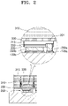
- FIG. 2 is an enlarged cross-sectional view of a portion of FIG. 1
- FIG. 3 is a perspective view of a partitioning wall structure applicable to the micro LED panel shown in FIG. 1 .
- the micro LED panel includes a backplane 100, a plurality of micro LED cells 200, a partitioning wall structure 300, and an adhesive member 330.
- a plurality of individually-driven LED driving circuits may be arranged in a matrix shape.
- the plurality of LED driving circuits may include a plurality of pairs of electrode units including a first electrode unit 120a and a second electrode unit 120b.
- a driving IC for controlling the operation of the plurality of micro LED cells 200 may be provided on the backplane 100.
- the plurality of micro LED cells 200 may be arranged in a matrix shape on the backplane 100, wherein the plurality of micro LED cells 200 may be arranged at positions respectively corresponding to the plurality of LED driving circuits of the backplane 100.
- Each of the plurality of micro LED cells 200 is configured to include both a first conductive type electrode pad 260a, which is bonded to the first electrode unit 120a of the backplane 100, and a second conductivity type electrode pad 260b, which is bonded to the second electrode unit 120b, on the bottom surface, and a light-emitting surface may be formed on the top surface of each of the plurality of micro LED cells 200.
- the plurality of micro LED cells 200 may be formed through cell separation of a gallium nitride-based semiconductor stack grown on a sapphire substrate, which is a growth substrate. A manufacturing method for separating a gallium nitride-based semiconductor stack will be described later in detail.
- Each of the plurality of micro LED cells 200 sequentially includes a first conductivity type semiconductor layer 210, an active layer 220, and a second conductivity type semiconductor layer 230 that are sequentially arranged in a direction away from a light-emitting surface 201.
- portions of the second conductivity type semiconductor layer 230 and the active layer 220 are selectively removed, and thus a portion of the first conductivity type semiconductor layer 210 is exposed toward the backplane 100, the first conductive type electrode pad 260a is connected to the first conductivity type semiconductor layer 210 through the exposed portion.
- the second conductivity type electrode pad 260b is connected to the second conductivity type semiconductor layer 230.
- a reflective layer and more preferably, distributed Bragg reflectors (DBR) may be formed to cover at least lower portions of the respective micro LED cells 200.
- DBR distributed Bragg reflectors
- the partitioning wall structure 300 may be positioned above the light-emitting surface 201 of the plurality of micro LED cells 200, and a plurality of first grooves 315 may be formed therein.
- the partitioning wall structure 300 includes a light-transmitting member 310 having a first surface 310a facing the light-emitting surface 201 and a second surface 310b facing the first surface 310a, and the plurality of first grooves 315 may be formed on the first surface 310a or the second surface 310b of the light-transmitting member 310.
- the light-transmitting member 310 may include a transmitting material that transmits light emitted from the micro LED cells 200 therethrough.
- the light-transmitting member 310 may include a glass material and may include a phosphor for individual wavelength conversion of light of each of the micro LED cells 200.
- the light-transmitting member 310 may include phosphor in glass (PIG).
- PIG is a composition in which a fluorescent material is mixed and dispersed and molded and sintered.
- deterioration and discoloration are less as compared to a conventional method of mixing an epoxy resin with a fluorescent material and then molding the same. Therefore a high power and high-efficiency LED package may be manufactured, the LED package exhibits high reliability at high temperatures.
- a fluorescent material is uniformly mixed with the glass in the PIG, an LED package having light uniformity and high brightness may be implemented. Therefore, the PIG may be applied to headlights of automobiles, flash lights of mobile phones for IT, high-power LED packages, etc.
- the light-transmitting member 310 may include, on any one of the first surface 310a and the second surface 310b, a plurality of first grooves 315 formed correspondingly among the plurality of micro LED cells 200.
- the length of the plurality of first grooves 315 may be extended in a direction from any one of the first surface 310a and the second surface 310b toward the other.
- the plurality of first grooves 315 may be formed in a structure surrounding the plurality of micro LED cells 200 arranged in a matrix shape. In other words, as shown in FIG. 3 , the plurality of first grooves 315 may form a grid structure like a checkerboard when viewed from above the first surface 310a or the second surface 310b.
- the plurality of first grooves 315 may be filled with a composition, from which a partitioning wall 320 that separates respective emission paths of light emitted from the plurality of micro LED cells 200 may be formed in the light-transmitting member 310.
- the light-transmitting member 310 may individually perform wavelength conversion on light (more particularly, blue light) emitted from a corresponding micro LED cell 200 through the partitioning wall 320, thereby generating white light.
- the partitioning wall 320 may include a composition that reflects or absorbs light emitted from the micro LED cells 200.
- the base material of the composition may be an organic or inorganic resin material.
- the composition may include an organic or inorganic resin material like silicone, epoxy, heat-resistant resin polyimide, phenol resin, melamine resin, unsaturated polyester resin, tritan.
- the composition may form black partitioning walls for absorbing light by using carbon or a carbon mixture or may form while partitioning walls for reflecting light by using titanium dioxide (TiO 2 ), barium sulfate (BaSO 4 ), etc.
- the composition may further include boron nitride (BN), aluminum nitride (AIN), aluminum (Al), graphite (Graphite), etc. Therefore, the light-transmitting member 310 may improve heat dissipation performance.
- the partitioning wall structure 300 may further include a substrate member 301 disposed on the second surface 310b of the light-transmitting member 310.
- the substrate member 301 may not only perform a function of supporting the light-transmitting member 310, but also perform a protection function like increasing the scratch resistance of the light-transmitting member 310.
- the substrate member 301 may include glass or a polymer material like polyethylene terephthalate (PET).
- the adhesive member 330 may be formed between the first surface 310a of the light-transmitting member 310 and the light-emitting surface 201 of the plurality of micro LED cells 200.
- the adhesive member 330 adheres the partitioning wall structure 300 and the plurality of micro LED cells 200 to each other.
- the adhesive member 330 may include a light-transmitting material through which light may be transmitted, e.g., a material like semi-cured silicone or epoxy.
- FIGS. 4 and 5 are diagrams for describing a method of manufacturing the partitioning wall structure stated above.
- the method of manufacturing a partitioning wall structure may include preparing the light-transmitting member 310, forming the plurality of first grooves 315 on the light-transmitting member 310, forming the partitioning wall 320 by filling the plurality of first grooves 315 with a composition, and disposing the adhesive member 330 on the first surface 310a of the light-transmitting member 310.
- the light-transmitting member 310 may be prepared on the substrate member 301.
- the light-transmitting member 310 is supported by the substrate member 301 and may be prepared in a state that the second surface 310b of the light-transmitting member 310 is contacting the substrate member 301.
- the technical spirit of the disclosure is not limited thereto.
- the substrate member 301 may be disposed on the second surface 310b of the light-transmitting member 310 after performing a process of forming the partitioning wall on the second surface 310b of the light-transmitting member 310, which is described later.
- descriptions below will focus on a method of forming the partitioning wall 320 on the first surface 310a of the light-transmitting member 310.
- the plurality of first grooves 315 are formed on the light-transmitting member 310, wherein the plurality of first grooves 315 may be cut-formed from the first surface 310a facing the second surface 310b of the light-transmitting member 310 to a pre-set depth.
- the plurality of first grooves 315 may be formed by using a contact or non-contact cutting device.
- the plurality of first grooves 315 may be cut-formed to a pre-set depth from the first surface 310a by using a contact cutting device 1 like a cutting blade.
- the plurality of first grooves 315 may be cut-formed to a pre-set depth from the first surface 310a by using a non-contact cutting device 2 like a laser source.
- the plurality of first grooves 315 formed through the above-described process may have a shape in which the width becomes narrower in a depth-wise direction away from the first surface 310a.
- the base material of the composition includes an organic or inorganic resin material, and the composition thereof may vary depending on whether the partitioning wall 320 is a reflective partitioning wall or an absorbing partitioning wall.
- the adhesive member 330 may be disposed on the first surface 310a of the light-transmitting member 310 and the partitioning wall structure 300 may be adhered to the plurality of micro LED cells 200 through the adhesive member 330.
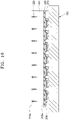
- FIGS. 6 to 11 are diagrams showing examples of a partitioning wall structure according to various embodiments of the disclosure.
- the partitioning wall structure 300 may include the light-transmitting member 310 in which partitioning walls 320 are formed, the adhesive member 330 disposed between the first surface 310a of the light-transmitting member 310 and light-emitting surfaces of the plurality of micro LED cells 200, and the substrate member 301 disposed on the light-transmitting member 310.
- the partitioning wall 320 may be formed by filling the plurality of first grooves 315 formed from the first surface 310a toward the second surface 310b of the light-transmitting member 310 with a composition.
- a depth d1 of the partitioning wall 320 may have a value between 1/2 times a thickness t of the light-transmitting member 310 and the thickness t.
- the light-transmitting member 310 may include a phosphor for individual wavelength conversion of light of each of the micro LED cells 200.
- the partitioning wall 320 may be formed by forming a plurality of second grooves 317 on the second surface 310b instead of the first surface 310a of the light-transmitting member 310 and filling the plurality of second grooves 317 with the composition.
- a depth d2 of the plurality of second grooves 317 may be less than 1/2 times the thickness t of the light-transmitting member 310.
- the partitioning wall structure may be stably manufactured by forming the plurality of second grooves 317 in the light-transmitting member 310 to a depth smaller than 1/2 times the thickness t of the light-transmitting member 310.
- the partitioning wall 320 may be formed by forming a plurality of grooves on both the first surface 310a and the second surface 310b of the light-transmitting member 310 and filling the plurality of grooves with a composition.
- the plurality of first grooves 315 may be formed on the first surface 310a of the light-transmitting member 310
- the plurality of second grooves 317 may be formed on the second surface 310b of the light-transmitting member 310.
- the plurality of first grooves 315 and the plurality of second grooves 317 may be symmetrically formed to face each other, and the plurality of first grooves 315 and the plurality of second grooves 317 facing each other do not contact each other.
- the partitioning wall structure of FIG. 8 may be manufactured by forming the plurality of second grooves 317 on the second surface 310b of the light-transmitting member 310 first and filling the plurality of second grooves 317 with a composition and then forming the plurality of first grooves 315 on the first surface 310a of the light-transmitting member 310 and filling the plurality of first grooves 315 with a composition.
- the substrate member 301 serving as the support member may be removed.
- the partitioning wall structure may include only the substrate member 301 and the adhesive member 330 without a separate light-transmitting member including a phosphor.
- the partitioning wall 320 is formed by forming grooves in the substrate member 301 by using a contact or non-contact cutting device and filling the grooves with a composition, and a phosphor may be included in the adhesive member 330.
- the plurality of first grooves 315 may include concavo-convex surfaces.
- concaveness and convexness may be formed in the plurality of first grooves 315 or the plurality of second grooves 317 (refer to FIG. 7 ) formed in the light-transmitting member 310 along cut surfaces. Due to the first grooves 315 or the second grooves 317 having the above-described shape, the partitioning wall 320 may scatter light emitted from each of the micro LED cells 200 and improve light efficiency.
- FIGS. 12 to 14 are diagrams for describing a method of manufacturing a micro LED panel according to an embodiment of the disclosure.
- the method of manufacturing a micro LED panel according to the present embodiment includes preparing a backplane, forming micro LED cells in a matrix shape at the bottom of a growth substrate, bonding the micro LED cells to the backplane, separating the growth substrate from the micro LED cells, and disposing a partitioning wall structure on the micro LED cells.
- a partitioning wall structure since the method of manufacturing the partitioning wall structure has been described above with reference to FIGS. 4 and 5 , descriptions identical to those given above will be omitted, and descriptions given below will focus on a process of forming micro LED cells and bonding the micro LED cells to a backplane with reference to FIGS. 12 to 14 .
- a gallium nitride-based semiconductor stack sequentially including the first conductivity type semiconductor layer 210, the active layer 220, and the second conductivity type semiconductor layer 230 is formed on a sapphire substrate serving as a growth substrate 20, and then, the gallium nitride-based semiconductor stack is divided into the plurality of micro LED cells 200 arranged in a matrix shape.
- an active layer of micro LED cells may be separated by removing a portion of the second conductivity type semiconductor layer 210 and the active layer 220. Therefore, both the first conductivity type semiconductor layer 210 and the second conductivity type semiconductor layer 230 of each micro LED cell 200 may be exposed toward the backplane 100 therebelow.
- the first conductivity type electrode pad 260a and the second conductivity type electrode pad 260b are formed by, for example, depositing a metal material and are formed to be connected to the first conductivity type semiconductor layer 210 and the second conductivity type semiconductor layer 230, respectively.
- the micro LED cells 200 may be separated from one another by removing a first conductivity type semiconductor layer 210a between the micro LED cells 200.
- FIG. 12 shows a state in which the first conductive type electrode pad 260a is connected to the first conductivity type semiconductor layer 210 and the second conductivity type electrode pad 260b is connected to the second conductivity type semiconductor layer 230 so as to illustrate the structure between the micro LED cells 200 and a method of removing the first conductivity type semiconductor layer 210a between the micro LED cells 200 is described above, the technical spirit of the disclosure is not limited thereto.
- the first conductivity type semiconductor layer 210 may be removed, and the first conductive type electrode pad 260a and the second conductivity type electrode pad 260b may be connected to exposed portions of the first conductivity type semiconductor layer 210 and the second conductivity type semiconductor layer 230, respectively.
- the method of manufacturing a micro LED panel includes bonding the first conductive type electrode pad 260a and the second conductivity type electrode pad 260b of each of the micro LED cells 200 to the first electrode unit 120a and the second electrode unit 120b of the backplane 100, respectively. Through this operation, the plurality of micro LED cells 200 arranged on the bottom surface of the growth substrate 20 in a matrix shape are mounted on the backplane 100.
- the method of manufacturing a micro LED panel may further include filling an adhesive material between the micro LED cells 200 after the micro LED cells 200, which are arranged on the growth substrate 20 in a matrix shape, are mounted on the backplane 100 and curing the adhesive material. Since the first conductivity type semiconductor layer 210 is completely removed between the micro LED cells 200, the micro LED cells 200 may be separated into individual micro LED cells 200 by the adhesive material injected therebetween. Therefore, a micro LED panel manufactured according to the present embodiment may minimize the light spreading phenomenon that may occur in the first conductivity type semiconductor layer. The injected adhesive material is cured to form an adhesive layer 270 disposed on the growth substrate 20 and the backplane 100.
- the method of manufacturing a micro LED panel includes separating and removing the growth substrate 20 from the micro LED cells 200.
- a laser lift off (LLO) process may be applied to separate the growth substrate 20.
- LLO laser lift off
- the growth substrate 20 is separated through the LLO process, since electrode pads respectively formed at the micro LED cells 200 are bonded to the electrode units of the backplane 100, displacement and undesired deformation of the micro LED cells 200 may be suppressed.
- the micro LED cells 200 are adhered to each other by using an adhesive material, defects due to separation of the growth substrate 20 may be suppressed.
- the method of manufacturing a micro LED panel includes disposing the partitioning wall structure 300 (refer to FIG. 1 ) over the micro LED cells 200 after the growth substrate 20 is removed.
- the partitioning wall structure 300 is closely attached to the top of the micro LED cells 200 through the adhesive member 330.
- the partitioning wall structure 300 uses the light-transmitting member 310 in which the partitioning walls 320 are formed to perform individual wavelength conversion on light emitted from each of the micro LED cells 200, thereby generating white light.
- partitioning walls are formed in a light-transmitting member including a phosphor without forming a separate partitioning wall structure, thereby simplifying the overall manufacturing process. Therefore, individual pixels may be implemented at inexpensive process costs.
- FIG. 15 is a diagram showing images of micro LED panels manufactured according to the present embodiment and a comparative example compared for each process.
- FIG. 15A is an image showing bottom surfaces of micro LED cells
- FIG. 15B is an image showing top surfaces of micro LED cells before removal of a growth substrate
- FIG. 15C is an image showing top surfaces of micro LED cells after removal of the growth substrate.
- a micro LED panel (I) according to the comparative example a plurality of micro LED cells are not completely separated from one another and a first conductivity type semiconductor layer remains therebetween.
- a first conductivity type semiconductor layer is removed between a plurality of micro LED cells, and thus clear dividing lines are formed therebetween. Due to the difference, according to a micro LED panel and a method of manufacturing a micro LED panel according to embodiments of the disclosure, light spreading phenomenon due to a first conductivity type semiconductor layer may be minimized by completely removing the first conductivity type semiconductor layer between micro LED cells.
- partitioning walls are formed in a light-transmitting member including a phosphor without forming a separate partitioning wall structure, thereby simplifying the overall manufacturing process. Therefore, individual pixels may be implemented at inexpensive process costs.
- light spreading phenomenon due to a first conductivity type semiconductor layer may be minimized by completely removing the first conductivity type semiconductor layer between micro LED cells.
Landscapes
- Led Device Packages (AREA)
Applications Claiming Priority (1)
| Application Number | Priority Date | Filing Date | Title |
|---|---|---|---|
| KR1020210029712A KR102920084B1 (ko) | 2021-03-05 | 2021-03-05 | 마이크로 엘이디 패널 및 이의 제조 방법 |
Publications (1)
| Publication Number | Publication Date |
|---|---|
| EP4053898A1 true EP4053898A1 (fr) | 2022-09-07 |
Family
ID=80953481
Family Applications (1)
| Application Number | Title | Priority Date | Filing Date |
|---|---|---|---|
| EP22160170.1A Pending EP4053898A1 (fr) | 2021-03-05 | 2022-03-04 | Panneau à micro-del et son procédé de fabrication |
Country Status (3)
| Country | Link |
|---|---|
| US (1) | US20220285326A1 (fr) |
| EP (1) | EP4053898A1 (fr) |
| KR (1) | KR102920084B1 (fr) |
Cited By (4)
| Publication number | Priority date | Publication date | Assignee | Title |
|---|---|---|---|---|
| GB2622794A (en) * | 2022-09-27 | 2024-04-03 | Smartkem Ltd | Selective transfer of micro-LEDs |
| WO2025196104A1 (fr) * | 2024-03-21 | 2025-09-25 | Valeo Vision | Module lumineux pour un dispositif de signalisation d'un vehicule automobile |
| WO2025196103A1 (fr) * | 2024-03-21 | 2025-09-25 | Valeo Vision | Module lumineux pour un dispositif de signalisation d'un vehicule automobile et son procédé de fabrication |
| WO2026074189A1 (fr) * | 2024-10-03 | 2026-04-09 | Valeo Vision | Module lumineux d'un dispositif de signalisation d'un véhicule automobile |
Families Citing this family (3)
| Publication number | Priority date | Publication date | Assignee | Title |
|---|---|---|---|---|
| WO2022212125A1 (fr) * | 2021-03-31 | 2022-10-06 | Apple Inc. | Couture enterrée avec motif de kirigami pour affichage micro-del 3d |
| CN114038977B (zh) * | 2021-08-04 | 2023-10-31 | 重庆康佳光电科技有限公司 | 发光器件的制作方法 |
| WO2026074191A1 (fr) * | 2024-10-03 | 2026-04-09 | Valeo Vision | Module lumineux d'un dispositif de signalisation d'un véhicule automobile |
Citations (5)
| Publication number | Priority date | Publication date | Assignee | Title |
|---|---|---|---|---|
| US8475023B2 (en) * | 2009-11-20 | 2013-07-02 | Koito Manufacturing Co., Ltd. | Light emitting module and automotive lamp |
| WO2014090893A1 (fr) * | 2012-12-12 | 2014-06-19 | Osram Opto Semiconductors Gmbh | Composant semi-conducteur optoélectronique et procédé de fabrication d'un composant semi-conducteur optoélectronique |
| US20170294418A1 (en) * | 2016-04-12 | 2017-10-12 | Cree, Inc. | High density pixelated led and devices and methods thereof |
| US20180012949A1 (en) * | 2016-07-06 | 2018-01-11 | Seoul Semiconductor Co., Ltd. | Display apparatus |
| US20190237637A1 (en) * | 2018-02-01 | 2019-08-01 | Epistar Corporation | Light-emitting device and manufacturing method thereof |
Family Cites Families (5)
| Publication number | Priority date | Publication date | Assignee | Title |
|---|---|---|---|---|
| CN113658943A (zh) * | 2013-12-13 | 2021-11-16 | 晶元光电股份有限公司 | 发光装置及其制作方法 |
| KR102252475B1 (ko) * | 2014-06-02 | 2021-05-17 | 엘지이노텍 주식회사 | 발광 소자 모듈 |
| WO2019078135A1 (fr) * | 2017-10-16 | 2019-04-25 | Nsマテリアルズ株式会社 | Feuille ou film de résine contenant des points quantiques, son procédé de fabrication et élément de conversion de longueur d'onde |
| CN110890453B (zh) * | 2018-09-07 | 2021-08-27 | 群创光电股份有限公司 | 显示装置 |
| KR102779280B1 (ko) * | 2019-05-03 | 2025-03-12 | 삼성전자주식회사 | Led 디스플레이 모듈, led 디스플레이 모듈의 제조 방법, 그리고 led 디스플레이 모듈을 포함하는 디스플레이 장치 |
-
2021
- 2021-03-05 KR KR1020210029712A patent/KR102920084B1/ko active Active
-
2022
- 2022-03-03 US US17/685,459 patent/US20220285326A1/en not_active Abandoned
- 2022-03-04 EP EP22160170.1A patent/EP4053898A1/fr active Pending
Patent Citations (5)
| Publication number | Priority date | Publication date | Assignee | Title |
|---|---|---|---|---|
| US8475023B2 (en) * | 2009-11-20 | 2013-07-02 | Koito Manufacturing Co., Ltd. | Light emitting module and automotive lamp |
| WO2014090893A1 (fr) * | 2012-12-12 | 2014-06-19 | Osram Opto Semiconductors Gmbh | Composant semi-conducteur optoélectronique et procédé de fabrication d'un composant semi-conducteur optoélectronique |
| US20170294418A1 (en) * | 2016-04-12 | 2017-10-12 | Cree, Inc. | High density pixelated led and devices and methods thereof |
| US20180012949A1 (en) * | 2016-07-06 | 2018-01-11 | Seoul Semiconductor Co., Ltd. | Display apparatus |
| US20190237637A1 (en) * | 2018-02-01 | 2019-08-01 | Epistar Corporation | Light-emitting device and manufacturing method thereof |
Cited By (8)
| Publication number | Priority date | Publication date | Assignee | Title |
|---|---|---|---|---|
| GB2622794A (en) * | 2022-09-27 | 2024-04-03 | Smartkem Ltd | Selective transfer of micro-LEDs |
| GB2622794B (en) * | 2022-09-27 | 2025-06-04 | Smartkem Ltd | Selective transfer of micro-LEDs |
| WO2025196104A1 (fr) * | 2024-03-21 | 2025-09-25 | Valeo Vision | Module lumineux pour un dispositif de signalisation d'un vehicule automobile |
| WO2025196103A1 (fr) * | 2024-03-21 | 2025-09-25 | Valeo Vision | Module lumineux pour un dispositif de signalisation d'un vehicule automobile et son procédé de fabrication |
| FR3160447A1 (fr) * | 2024-03-21 | 2025-09-26 | Valeo Vision | Module lumineux d’un dispositif de signalisation d’un véhicule automobile. |
| FR3160448A1 (fr) * | 2024-03-21 | 2025-09-26 | Valeo Vision | Module lumineux d’un dispositif de signalisation d’un véhicule automobile. |
| WO2026074189A1 (fr) * | 2024-10-03 | 2026-04-09 | Valeo Vision | Module lumineux d'un dispositif de signalisation d'un véhicule automobile |
| FR3167193A1 (fr) * | 2024-10-03 | 2026-04-10 | Valeo Vision | Module lumineux d’un dispositif de signalisation d’un véhicule automobile |
Also Published As
| Publication number | Publication date |
|---|---|
| US20220285326A1 (en) | 2022-09-08 |
| KR20220125618A (ko) | 2022-09-14 |
| KR102920084B1 (ko) | 2026-02-02 |
Similar Documents
| Publication | Publication Date | Title |
|---|---|---|
| EP4053898A1 (fr) | Panneau à micro-del et son procédé de fabrication | |
| EP3790062B1 (fr) | Dispositif d'affichage à cristaux liquides avec unité de rétroéclairage ayant des dispositifs électroluminescents | |
| JP6595055B2 (ja) | 発光デバイス及び波長変換材料を含む光共振器 | |
| JP6680349B1 (ja) | 発光モジュール | |
| US7646035B2 (en) | Packaged light emitting devices including multiple index lenses and multiple index lenses for packaged light emitting devices | |
| US20230220975A1 (en) | Light source device and lens structure | |
| KR101850431B1 (ko) | 발광 모듈 및 이를 포함하는 조명 시스템 | |
| JP5458044B2 (ja) | 発光素子および発光素子の製造方法 | |
| KR102285432B1 (ko) | 발광소자 패키지 | |
| US9705050B2 (en) | Phosphor sheet, light-emitting device having the phosphor sheet and method of manufacturing the same | |
| JP2018107257A (ja) | 発光装置 | |
| CN111668201A (zh) | 发光模块 | |
| KR20160054776A (ko) | 발광 모듈, 이 모듈을 포함하는 백 라이트 유닛 및 이 유닛을 포함하는 표시 장치 | |
| KR101575655B1 (ko) | 발광 소자 패키지 및 백라이트 유닛 | |
| KR102252475B1 (ko) | 발광 소자 모듈 | |
| KR20250145505A (ko) | 발광 장치 및 면형상 광원 | |
| KR102194803B1 (ko) | 발광 소자 패키지 | |
| KR101575653B1 (ko) | 발광 소자 패키지, 백라이트 유닛, 조명 장치 및 발광 소자 패키지의 제작 방법 | |
| JP2026503026A (ja) | 発光ダイオードデバイスの側壁配置および関連する方法 | |
| KR101850435B1 (ko) | 발광 모듈 및 이를 포함하는 표시 장치 | |
| US12433076B2 (en) | Light-emitting device package for back light and manufacturing method thereof | |
| KR20210117791A (ko) | 마이크로 엘이디 패널 | |
| KR102160774B1 (ko) | 발광 소자 패키지 및 그 제조방법 | |
| US20230317909A1 (en) | Light-emitting module and method for manufacturing light-emitting module | |
| KR102211319B1 (ko) | Led 모듈 |
Legal Events
| Date | Code | Title | Description |
|---|---|---|---|
| PUAI | Public reference made under article 153(3) epc to a published international application that has entered the european phase |
Free format text: ORIGINAL CODE: 0009012 |
|
| STAA | Information on the status of an ep patent application or granted ep patent |
Free format text: STATUS: REQUEST FOR EXAMINATION WAS MADE |
|
| 17P | Request for examination filed |
Effective date: 20220304 |
|
| AK | Designated contracting states |
Kind code of ref document: A1 Designated state(s): AL AT BE BG CH CY CZ DE DK EE ES FI FR GB GR HR HU IE IS IT LI LT LU LV MC MK MT NL NO PL PT RO RS SE SI SK SM TR |