EP4055426B1 - Facilitation de la formation d'un trou d'interconnexion dans un substrat - Google Patents
Facilitation de la formation d'un trou d'interconnexion dans un substrat Download PDFInfo
- Publication number
- EP4055426B1 EP4055426B1 EP20884706.1A EP20884706A EP4055426B1 EP 4055426 B1 EP4055426 B1 EP 4055426B1 EP 20884706 A EP20884706 A EP 20884706A EP 4055426 B1 EP4055426 B1 EP 4055426B1
- Authority
- EP
- European Patent Office
- Prior art keywords
- inorganic substrate
- opening
- diameter
- pathway
- substrate
- Prior art date
- Legal status (The legal status is an assumption and is not a legal conclusion. Google has not performed a legal analysis and makes no representation as to the accuracy of the status listed.)
- Active
Links
Images




Classifications
-
- B—PERFORMING OPERATIONS; TRANSPORTING
- B23—MACHINE TOOLS; METAL-WORKING NOT OTHERWISE PROVIDED FOR
- B23K—SOLDERING OR UNSOLDERING; WELDING; CLADDING OR PLATING BY SOLDERING OR WELDING; CUTTING BY APPLYING HEAT LOCALLY, e.g. FLAME CUTTING; WORKING BY LASER BEAM
- B23K26/00—Working by laser beam, e.g. welding, cutting or boring
- B23K26/36—Removing material
- B23K26/40—Removing material taking account of the properties of the material involved
- B23K26/402—Removing material taking account of the properties of the material involved involving non-metallic material, e.g. isolators
-
- B—PERFORMING OPERATIONS; TRANSPORTING
- B23—MACHINE TOOLS; METAL-WORKING NOT OTHERWISE PROVIDED FOR
- B23K—SOLDERING OR UNSOLDERING; WELDING; CLADDING OR PLATING BY SOLDERING OR WELDING; CUTTING BY APPLYING HEAT LOCALLY, e.g. FLAME CUTTING; WORKING BY LASER BEAM
- B23K26/00—Working by laser beam, e.g. welding, cutting or boring
- B23K26/02—Positioning or observing the workpiece, e.g. with respect to the point of impact; Aligning, aiming or focusing the laser beam
- B23K26/06—Shaping the laser beam, e.g. by masks or multi-focusing
- B23K26/062—Shaping the laser beam, e.g. by masks or multi-focusing by direct control of the laser beam
- B23K26/0622—Shaping the laser beam, e.g. by masks or multi-focusing by direct control of the laser beam by shaping pulses
- B23K26/0624—Shaping the laser beam, e.g. by masks or multi-focusing by direct control of the laser beam by shaping pulses using ultrashort pulses, i.e. pulses of 1 ns or less
-
- B—PERFORMING OPERATIONS; TRANSPORTING
- B23—MACHINE TOOLS; METAL-WORKING NOT OTHERWISE PROVIDED FOR
- B23K—SOLDERING OR UNSOLDERING; WELDING; CLADDING OR PLATING BY SOLDERING OR WELDING; CUTTING BY APPLYING HEAT LOCALLY, e.g. FLAME CUTTING; WORKING BY LASER BEAM
- B23K26/00—Working by laser beam, e.g. welding, cutting or boring
- B23K26/36—Removing material
- B23K26/38—Removing material by boring or cutting
- B23K26/382—Removing material by boring or cutting by boring
-
- B—PERFORMING OPERATIONS; TRANSPORTING
- B23—MACHINE TOOLS; METAL-WORKING NOT OTHERWISE PROVIDED FOR
- B23K—SOLDERING OR UNSOLDERING; WELDING; CLADDING OR PLATING BY SOLDERING OR WELDING; CUTTING BY APPLYING HEAT LOCALLY, e.g. FLAME CUTTING; WORKING BY LASER BEAM
- B23K26/00—Working by laser beam, e.g. welding, cutting or boring
- B23K26/50—Working by transmitting the laser beam through or within the workpiece
- B23K26/53—Working by transmitting the laser beam through or within the workpiece for modifying or reforming the material inside the workpiece, e.g. for producing break initiation cracks
-
- C—CHEMISTRY; METALLURGY
- C03—GLASS; MINERAL OR SLAG WOOL
- C03C—CHEMICAL COMPOSITION OF GLASSES, GLAZES OR VITREOUS ENAMELS; SURFACE TREATMENT OF GLASS; SURFACE TREATMENT OF FIBRES OR FILAMENTS MADE FROM GLASS, MINERALS OR SLAGS; JOINING GLASS TO GLASS OR OTHER MATERIALS
- C03C15/00—Surface treatment of glass, not in the form of fibres or filaments, by etching
-
- C—CHEMISTRY; METALLURGY
- C03—GLASS; MINERAL OR SLAG WOOL
- C03C—CHEMICAL COMPOSITION OF GLASSES, GLAZES OR VITREOUS ENAMELS; SURFACE TREATMENT OF GLASS; SURFACE TREATMENT OF FIBRES OR FILAMENTS MADE FROM GLASS, MINERALS OR SLAGS; JOINING GLASS TO GLASS OR OTHER MATERIALS
- C03C23/00—Other surface treatment of glass not in the form of fibres or filaments
- C03C23/0005—Other surface treatment of glass not in the form of fibres or filaments by irradiation
- C03C23/0025—Other surface treatment of glass not in the form of fibres or filaments by irradiation by a laser beam
-
- C—CHEMISTRY; METALLURGY
- C03—GLASS; MINERAL OR SLAG WOOL
- C03C—CHEMICAL COMPOSITION OF GLASSES, GLAZES OR VITREOUS ENAMELS; SURFACE TREATMENT OF GLASS; SURFACE TREATMENT OF FIBRES OR FILAMENTS MADE FROM GLASS, MINERALS OR SLAGS; JOINING GLASS TO GLASS OR OTHER MATERIALS
- C03C23/00—Other surface treatment of glass not in the form of fibres or filaments
- C03C23/0005—Other surface treatment of glass not in the form of fibres or filaments by irradiation
- C03C23/006—Other surface treatment of glass not in the form of fibres or filaments by irradiation by plasma or corona discharge
-
- C—CHEMISTRY; METALLURGY
- C03—GLASS; MINERAL OR SLAG WOOL
- C03C—CHEMICAL COMPOSITION OF GLASSES, GLAZES OR VITREOUS ENAMELS; SURFACE TREATMENT OF GLASS; SURFACE TREATMENT OF FIBRES OR FILAMENTS MADE FROM GLASS, MINERALS OR SLAGS; JOINING GLASS TO GLASS OR OTHER MATERIALS
- C03C23/00—Other surface treatment of glass not in the form of fibres or filaments
- C03C23/0075—Cleaning of glass
-
- H—ELECTRICITY
- H10—SEMICONDUCTOR DEVICES; ELECTRIC SOLID-STATE DEVICES NOT OTHERWISE PROVIDED FOR
- H10W—GENERIC PACKAGES, INTERCONNECTIONS, CONNECTORS OR OTHER CONSTRUCTIONAL DETAILS OF DEVICES COVERED BY CLASS H10
- H10W70/00—Package substrates; Interposers; Redistribution layers [RDL]
- H10W70/01—Manufacture or treatment
- H10W70/05—Manufacture or treatment of insulating or insulated package substrates, or of interposers, or of redistribution layers
- H10W70/095—Manufacture or treatment of insulating or insulated package substrates, or of interposers, or of redistribution layers of vias therein
-
- H—ELECTRICITY
- H10—SEMICONDUCTOR DEVICES; ELECTRIC SOLID-STATE DEVICES NOT OTHERWISE PROVIDED FOR
- H10W—GENERIC PACKAGES, INTERCONNECTIONS, CONNECTORS OR OTHER CONSTRUCTIONAL DETAILS OF DEVICES COVERED BY CLASS H10
- H10W70/00—Package substrates; Interposers; Redistribution layers [RDL]
- H10W70/60—Insulating or insulated package substrates; Interposers; Redistribution layers
- H10W70/62—Insulating or insulated package substrates; Interposers; Redistribution layers characterised by their interconnections
- H10W70/63—Vias, e.g. via plugs
- H10W70/635—Through-vias
-
- H—ELECTRICITY
- H10—SEMICONDUCTOR DEVICES; ELECTRIC SOLID-STATE DEVICES NOT OTHERWISE PROVIDED FOR
- H10W—GENERIC PACKAGES, INTERCONNECTIONS, CONNECTORS OR OTHER CONSTRUCTIONAL DETAILS OF DEVICES COVERED BY CLASS H10
- H10W70/00—Package substrates; Interposers; Redistribution layers [RDL]
- H10W70/60—Insulating or insulated package substrates; Interposers; Redistribution layers
- H10W70/67—Insulating or insulated package substrates; Interposers; Redistribution layers characterised by their insulating layers or insulating parts
- H10W70/69—Insulating materials thereof
- H10W70/692—Ceramics or glasses
-
- B—PERFORMING OPERATIONS; TRANSPORTING
- B23—MACHINE TOOLS; METAL-WORKING NOT OTHERWISE PROVIDED FOR
- B23K—SOLDERING OR UNSOLDERING; WELDING; CLADDING OR PLATING BY SOLDERING OR WELDING; CUTTING BY APPLYING HEAT LOCALLY, e.g. FLAME CUTTING; WORKING BY LASER BEAM
- B23K2103/00—Materials to be soldered, welded or cut
- B23K2103/50—Inorganic materials other than metals or composite materials
- B23K2103/54—Glass
Definitions
- aspects of this disclosure generally are related to the formation of one or more vias in a substrate, such as an inorganic substrate, which may be glass.
- Insulating substrates with precisely formed and positioned through-holes, or vias have many applications in electronic and photonic packaging.
- a throughsubstrate via can be filled with conductive material to provide a vertical electrical connection that passes completely through the substrate.
- a via may be a hole through the substrate that is large enough to fill with conductive material, in order to conduct electrical signals from one surface of the substrate to the other.
- Glass has many advantages as a substrate, including that it can be formed in large sheets of uniform thickness with very smooth surfaces, is dimensionally stable, and relatively rigid. Glass can be formed with those good properties at thicknesses well below 0.5 mm.
- the through-holes to be filled with conductive material can be formed by a variety of methods, including lithography of photolithographic glass, sand-blasting, electric discharge drilling, swift heavy ion tracks, and many versions of laser drilling.
- the holes are formed to the correct opening size directly.
- the positions of the vias are established by a method which creates a damage track or preformed opening or pilot hole in the glass, while a subsequent wet etching process enlarges the damage track to create a through-hole with the desired diameter.
- the details of the via formation typically have to be carefully designed to create smooth, circular, vias of the correct opening diameter with low cracking around the holes.
- FIGS. 1A-1C illustrate a conventional via formation process, where, as shown in FIG. 1A , a single-sided wet-etching process is applied to a first surface 400a of a glass substrate 400 having a damage track 40 formed therein to create a via 45 ( FIG. 1B ). To protect the second surface 400b from the wet-etching process, a sealant material layer 450 is applied to the second surface 400b.
- the etch When substrate 400 is immersed in etch solution, the etch will begin at the exposed surface 400a and progress so that the largest diameter of the via 45 is at the top first surface 400a, represented by opening 45a of via 45 in FIG. 1B .
- the etching must continue to be applied further to enlarge the opening 45b in FIG. 1B on the sealed second surface 400b to the desired diameter, 20tb shown in FIG. 1C .
- This added duration of the wet etch means that the top diameter 20ra in FIG. 1B also continues to grow to a potentially undesired diameter 20ta as shown in FIG. 1C , resulting in a tapered through-hole.
- the present inventors recognized that one potential difficulty of this single-sided wet etching process is that the final diameter of the top opening of the via 45 in the exposed first surface 400a is dependent on the thickness 410 of the substrate 400 and the desired diameter of the bottom opening of the via 45 in the sealed second surface 400b.
- the density of vias in the substrate 400 is limited by this conventional single-sided wet etching process due to the relatively large size of the via openings (e.g., opening 45a) in the exposed first surface 400a of the substrate 400, and the achievable size of via 45 is tied directly to and possibly limited by the thickness 410 of the substrate 400.
- the diameter 20ta of the top opening 45a of the via 45 is much smaller than the diameter 59 of the laterally-etched region 47.
- the present inventors recognize that the presence of such a large undercut or laterally-etched region 47 is not preferred and can be harmful to performance.
- the present inventors recognized that the conventional single sided wet etching process of FIGS. 1A-1C is less preferable due at least to the presence of the large undercutting or laterally-etched region 47 and the relatively large diameter 20ta exhibited by the opening 45a in the exposed first surface 400a of the substrate 400, which limits via density.
- the present inventors also recognized that a lack of control exists over opening diameter 20ta, which is dependent on the thickness 410 of the substrate 400.
- Patent application US 2019/185373 A1 discloses methods of forming vias in a glass-based article by laser-damage-and-etch processes including etching solutions having positive charge organic molecules.
- a method of forming a via in a glass-based article includes forming a damage track through a bulk of the glass-based article extending from a first surface of the glass-based article to a second surface of the glass-based article, and applying an etching solution to the glass-based article to form the via.
- the etching solution includes at least one acid and a positive charge organic molecule.
- An etch rate at the first surface and the second surface is lower than an etch rate at the damage track.
- a method of facilitating formation of a via in an inorganic substrate includes applying a double-sided opening process to the inorganic substrate.
- the inorganic substrate may include a damage track including a first end in a first surface of the inorganic substrate and a second end in a second surface of the inorganic substrate.
- the second surface may be on an opposite side of the inorganic substrate than the first surface of the inorganic substrate.
- the double-sided opening process may enlarge at least a first dimension of the first end of the damage track to form a first opening in the first surface of the inorganic substrate.
- the first dimension of the first end of the damage track may be measured within a plane of the first surface of the inorganic substrate.
- the double-sided opening process may enlarge at least a first dimension of the second end of the damage track to form a first opening in the second surface of the inorganic substrate.
- the first dimension of the second end of the damage track may be measured within a plane of the second surface of the inorganic substrate.
- a pathway may extend between the first opening in the first surface of the inorganic substrate and the first opening in the second surface of the inorganic substrate.
- the pathway may include a longitudinal axis perpendicular to (a) an extension direction of the first surface of the inorganic substrate, (b) an extension direction of the second surface of the inorganic substrate, or both (a) and (b).
- the pathway may include varying diameters of lateral cross-sections taken perpendicular to the longitudinal axis of the pathway, and the pathway may include a waist coinciding with a lateral cross-section of the pathway taken perpendicular to the longitudinal axis at a point of minimum diameter of the varying diameters of the pathway.
- the method may include applying a single-sided opening process to the first surface of the inorganic substrate, after completion of the double-sided opening process.
- the single-sided opening process may enlarge at least a first dimension of the first opening in the first surface of the inorganic substrate to form a second opening in the first surface of the inorganic substrate.
- the single-sided opening enlargement process may move the waist of the pathway closer to the second surface of the inorganic substrate as compared to a location of the waist after completion of the double-sided opening process but before applying the single-sided opening process.
- the moving of the waist may form a resultant pathway.
- the single-sided opening process may cause a via formed in the inorganic substrate to comprise the second opening in the first surface of the inorganic substrate, a resultant second opening in the second surface of the inorganic substrate, and the resultant pathway.
- the resultant pathway may extend from the second opening in the first surface of the inorganic substrate to the resultant second opening in the second surface of the inorganic substrate.
- the double-sided opening process includes a wet etching process concurrently applied to the first surface of the inorganic substrate and the second surface of the inorganic substrate.
- the wet etching process includes application of an etching composition comprising an HF concentration less than 1M and a strong acid concentration greater than 0.8M.
- the single-sided opening process comprises a wet etching process applied to the first surface of the inorganic substrate, but not to the second surface of the inorganic substrate.
- the inorganic substrate is glass.
- the damage track is or was formed by a laser.
- a ratio of (a) a diameter of the first opening in the first surface of the inorganic substrate to (b) a diameter of the first opening in the second surface of the inorganic substrate is in a range of 0.7 to 1.3, and the diameter of the first opening in the first surface of the inorganic substrate and the diameter of the first opening in the second surface of the inorganic substrate are measured along parallel line segments.
- a ratio of (a) a diameter of the second opening in the first surface of the inorganic substrate to (b) a diameter of the resultant second opening in the second surface of the inorganic substrate is in a range of 1.2 to 3, and the diameter of the second opening in the first surface of the inorganic substrate and the diameter of the resultant second opening in the second surface of the inorganic substrate are measured along parallel line segments.
- a ratio of (a) a diameter of the second opening in the first surface of the inorganic substrate to (b) a diameter of the waist of the resultant pathway upon completion of the single-sided opening process is in a range of 1.2 to 3, and the diameter of the second opening in the first surface of the inorganic substrate and the diameter of the waist of the resultant pathway are measured along parallel line segments.
- a diameter of the second opening in the first surface of the inorganic substrate is at least 25% larger than a corresponding diameter of the resultant second opening in the second surface of the inorganic substrate, and the diameter of the second opening in the first surface of the inorganic substrate and the corresponding diameter of the resultant second opening in the second surface of the inorganic substrate are measured along parallel line segments.
- a diameter of the first opening in the second surface of the inorganic substrate is within 20% of a corresponding diameter of the resultant second opening in the second surface of the inorganic substrate, and the diameter of the first opening in the second surface of the inorganic substrate and the corresponding diameter of the resultant second opening in the second surface of the inorganic substrate are measured along parallel line segments.
- the resultant pathway after completion of the single-sided opening process, has a trumpet shape or a conical frustum shape. In some examples, after completion of the double-sided opening process but before application of the single-sided opening process, the pathway has an hourglass shape.
- a longitudinal cross-section of the pathway taken along the longitudinal axis of the pathway does not have a trumpet shape and does not have a conical frustum shape.
- the method further includes bonding a semiconductor substrate to the second surface of the inorganic substrate after completion of the double-sided opening process, but before applying the single-sided opening process.
- the bonding is Van der Waals bonding or Van der Waals bonding assisted by covalent bonding.
- the method further includes temporarily bonding the inorganic substrate to a semiconductor substrate using a deposited carbonaceous layer.
- the semiconductor substrate is silicon.
- the deposited carbonaceous layer comprises an amorphous carbon, an amorphous hydrogenated carbon, a diamond, a diamond-like carbon, or a fluorine containing carbon film.
- the semiconductor substrate is silicon, and the deposited carbonaceous layer comprises an amorphous carbon, an amorphous hydrogenated carbon, a diamond, a diamond-like carbon, or a fluorine containing carbon film.
- a cross-section of the second opening in the first surface of the inorganic substrate, taken perpendicular to a longitudinal axis of the resultant pathway, has a circular shape, the longitudinal axis of the resultant pathway perpendicular to (c) an extension direction of the first surface of the inorganic substrate, (d) an extension direction of the second surface of the inorganic substrate, or both (c) and (d).
- a cross-section of the resultant second opening in the second surface of the inorganic substrate, taken perpendicular to a longitudinal axis of the pathway, has a circular shape, the longitudinal axis of the resultant pathway perpendicular to (c) an extension direction of the first surface of the inorganic substrate, (d) an extension direction of the second surface of the inorganic substrate, or both (c) and (d).
- the method further includes, after completion of the double-sided opening process, but before applying the single-sided opening process, depositing an inorganic carbon-containing film on a surface of a blocking substrate and bonding the inorganic carbon-containing film to the second surface of the inorganic substrate.
- the double-sided opening process produces a via through the inorganic substrate from the damage track.
- the single-sided opening process occurs with etching conditions exhibiting a Thiele modulus greater than 1.1. In some examples, the single-sided opening process occurs with etching conditions exhibiting a Thiele modulus in a range of 1.1 to 10, inclusive. In some examples, the single-sided opening process occurs with etching conditions exhibiting a Thiele modulus in a range of 2 to 10, inclusive. In some examples, the double-sided opening process occurs with etching conditions exhibiting a Thiele modulus less than 0.9. In some examples, the double-sided opening process occurs with etching conditions exhibiting a Thiele modulus in a range of 0.1 to 0.9, inclusive.
- the double-sided opening process occurs with etching conditions exhibiting a Thiele modulus in a range of 0.1 to 0.5, inclusive.
- etching conditions exhibiting a Thiele modulus in a range of 0.1 to 0.5, inclusive.
- Various examples exhibit all possible permutations of the double-sided opening process and single-sided opening process Thiele modulus ranges included in this paragraph.
- a method of facilitating formation of a via in an inorganic substrate includes bonding a semiconductor substrate to a second surface of the inorganic substrate.
- the inorganic substrate may include a first opening in a first surface of the inorganic substrate, the second surface on an opposite side of the inorganic substrate than the first surface of the inorganic substrate.
- the inorganic substrate includes a first opening in the second surface of the inorganic substrate and includes a via including the first opening in the first surface of the inorganic substrate, the first opening in the second surface of the inorganic substrate, and a channel extending from the first opening in the first surface of the inorganic substrate at least toward the first opening in the second surface of the inorganic substrate.
- the channel may include a longitudinal axis perpendicular to (a) an extension direction of the first surface of the inorganic substrate, (b) an extension direction of the second surface of the inorganic substrate, or both (a) and (b).
- the channel may include varying diameters of lateral cross-sections taken perpendicular to the longitudinal axis of the channel.
- the via may include a waist coinciding with a lateral cross-section taken perpendicular to the longitudinal axis at a point of minimum diameter of the varying diameters of the channel.
- the method may include applying a single-sided opening process to the first surface of the inorganic substrate, after the bonding of the semiconductor substrate to the second surface of the inorganic substrate.
- a cross-section of the second opening in the first surface of the inorganic substrate, taken perpendicular to the longitudinal axis of the channel, has a circular shape.
- a cross-section of the resultant second opening in the second surface of the inorganic substrate, taken perpendicular to the longitudinal axis of the channel, has a circular shape.
- the bonding includes depositing an inorganic carbon-containing film on a surface of the semiconductor substrate, and bonding the inorganic carbon-containing film to the second surface of the inorganic substrate.
- the single-sided opening process occurs with etching conditions exhibiting a Thiele modulus greater than 1.1.
- a semiconductor apparatus or semiconductor includes an inorganic substrate and a semiconductor substrate bonded to a second surface of the inorganic substrate.
- the second surface of the inorganic substrate is on an opposite side of the inorganic substrate than a first surface of the inorganic substrate.
- the inorganic substrate may include a via that includes a channel that extends from an opening in the first surface of the inorganic substrate to an opening in the second surface of the inorganic substrate.
- the channel may include varying diameters of lateral cross-sections taken perpendicular to a longitudinal axis of the channel.
- the longitudinal axis of the channel may be perpendicular to (a) an extension direction of the first surface of the inorganic substrate, (b) an extension direction of the second surface of the inorganic substrate, or both (a) and (b).
- the via may include a waist coinciding with a lateral cross-section taken perpendicular to the longitudinal axis at a point of minimum diameter of the varying diameters of the channel.
- a first angle of a first portion of a wall of the via at the opening in the first surface of the inorganic substrate may be two (2) or more degrees in some examples, and four (4) or more degrees in some examples, greater than a second angle of a second portion of the wall of the via at the opening in the second surface of the inorganic substrate.
- Each of the first angle and the second angle may be taken between (i) the first portion or the second portion, respectively, of the wall of the via, and (ii) the longitudinal axis of the via.
- the first angle of the first portion of the wall of the via at the opening in the first surface of the inorganic substrate is between two (2) to eight (8) degrees (inclusive) greater than the second angle of the second portion of the wall of the via at the opening in the second surface of the inorganic substrate. In some examples, the first angle of the first portion of the wall of the via at the opening in the first surface of the inorganic substrate is between four (4) to eight (8) degrees (inclusive) greater than the second angle of the second portion of the wall of the via at the opening in the second surface of the inorganic substrate.
- the inorganic substrate is glass.
- a ratio of (a) a diameter of the opening in the first surface of the inorganic substrate to (b) a diameter of the opening in the second surface of the inorganic substrate is in a range of 1.2 to 3, and the diameter of the opening in the first surface of the inorganic substrate and the diameter of the opening in the second surface of the inorganic substrate are measured along parallel line segments.
- a ratio of (a) a diameter of the opening in the first surface of the inorganic substrate to (b) a diameter of the waist of the via is in a range of 1.2 to 3, and the diameter of the opening in the first surface of the inorganic substrate and the diameter of the waist of the via are measured along parallel line segments.
- a diameter of the opening in the first surface of the inorganic substrate is at least 25% larger than a corresponding diameter of the opening in the second surface of the inorganic substrate, and the diameter of the opening in the first surface of the inorganic substrate and the corresponding diameter of the opening in the second surface of the inorganic substrate are measured along parallel line segments.
- the via has a trumpet shape or a conical frustum shape.
- the semiconductor substrate is silicon
- a cross-section of the opening in the first surface of the inorganic substrate, taken perpendicular to the longitudinal axis of the via, has a circular shape.
- a thickness of the inorganic substrate is between 300 micrometers and 10 micrometers.
- Various examples may include apparatuses, systems, devices, or machines that are or include combinations or subsets of any one or more of the apparatuses, systems, devices, or machines and associated features thereof summarized above or otherwise described herein.
- an inventive single-sided opening process may be applied to the unsealed 'top' surface or side of the substrate.
- the SSOP may enlarge the opening in the 'top' unsealed surface or side of the substrate for each via, while moving the 'waist' of the respective via closer to the 'bottom' sealed surface or side of the substrate, providing a conical frustum or trumpet shape to each via, according to some embodiments.
- application of the DSOP followed by the SSOP provides greater control over the diameter of the 'top' opening of the via at least by making the diameter of the 'top' opening less dependent on the thickness of the substrate, allowing the option for a reduced diameter of the 'top' opening of the via and greater via density in the substrate as compared to the conventional solely single-sided etch via formation process above with respect to FIGS. 1A-1C .
- inventive SSOP can be applied for a shorter duration than the conventional solely single-sided etch described above with respect to FIGS. 1A-1C , since the DSOP provides initial openings at both ends of the via, and therefore, the SSOP is not necessarily responsible for having to etch all the way through the substrate and then to enlarge the farther end of the via, as in the conventional solely single-sided etch described above with respect to FIGS. 1A-1C .
- the etch chemistry of the SSOP can be adjusted relative to that of the DSOP, according to various embodiments, to change the etch rate of the portion of the via near the "bottom" or blocked substrate surface relative to that at the top, exposed surface, and thus shape the via advantageously.
- the DSOP utilize etch conditions that have a constant etch rate along the length of the via
- the SSOP may utilize etch conditions which act predominantly on the top opening of the via.
- the etch conditions have the most constant etch rate along the length of the via in order to minimize the size of the via opening in the top surface, which is opposite to the etch conditions selected for the SSOP etch in various embodiments of the present invention.
- inventive SSOP can be applied for a relatively shorter duration, the presence of undercutting or lateral etching at the interface between the bottom sealed surface of the substrate and the seal is reduced, which provides, at least in part, the improved via shape as compared to the conventional solely single-sided etch described above with respect to FIGS. 1A-1C . It should be noted that the invention is not limited to these or any other examples or embodiments provided herein, which are referred to for purposes of illustration only.
- any reference throughout this specification to "one embodiment”, “an embodiment”, “an example embodiment”, “an illustrated embodiment”, “a particular embodiment”, and the like means that a particular feature, structure or characteristic described in connection with the embodiment is included in at least one embodiment.
- any appearance of the phrase “in one embodiment”, “in an embodiment”, “in an example embodiment”, “in this illustrated embodiment”, “in this particular embodiment”, or the like in this specification is not necessarily all referring to one embodiment or a same embodiment.
- the particular features, structures or characteristics of different embodiments may be combined in any suitable manner to form one or more other embodiments.
- the word “or” is used in this disclosure in a non-exclusive sense.
- the word “set” is intended to mean one or more.
- the phrase, "a set of objects” means one or more of the objects.
- the phrase "at least” is or may be used herein at times merely to emphasize the possibility that other elements may exist besides those explicitly listed. However, unless otherwise explicitly noted (such as by the use of the term “only”) or required by context, non-usage herein of the phrase “at least” nonetheless includes the possibility that other elements may exist besides those explicitly listed.
- the phrase, 'based at least on A' includes A as well as the possibility of one or more other additional elements besides A.
- the phrase, 'based on A' includes A, as well as the possibility of one or more other additional elements besides A.
- the phrase, 'based only on A' includes only A.
- the phrase 'configured at least to A' includes a configuration to perform A, as well as the possibility of one or more other additional actions besides A.
- the phrase 'configured to A' includes a configuration to perform A, as well as the possibility of one or more other additional actions besides A.
- the phrase, 'configured only to A' means a configuration to perform only A.
- phrase "in response to” may be used in this disclosure.
- this phrase may be used in the following context, where an event A occurs in response to the occurrence of an event B.
- such phrase includes, for example, that at least the occurrence of the event B causes or triggers the event A.
- FIG. 2 illustrates methods of facilitating formation of a via in a substrate, according to some embodiments of the present invention.
- FIG. 2 includes four blocks, block 202, block 204, block 206, and block 208 in an illustrated sequence, each block corresponding to respective actions, various embodiments of the present invention include a subset (one or more) of such blocks in same or different sequences (when more than two blocks are included). It should be noted that each block in FIG. 2 may be considered a method step, according to some embodiments. Further, various embodiments of the present invention are not limited to one, or more, or all of the actions shown in the blocks of FIG. 2 , and some embodiments of the present invention include other actions described herein not shown in FIG. 2 in addition to or in lieu of the actions shown in FIG. 2 . In this regard, FIG. 2 is provided merely for illustration purposes and is not limiting.
- block 202 may include, according to some embodiments, obtaining an inorganic substrate, such as glass, including damage or pilot tracks (or pilot holes) at specified locations through the substrate where vias are desired.
- damage track will be intended to include a damage track, a pilot track, or a pilot hole, according to various respective embodiments.
- FIG. 3 illustrates a damage track 10 (illustrated in bold broken line) proceeding all the way through the thickness 110 of an inorganic substrate 100, according to some embodiments.
- the inorganic substrate 100 may be any inorganic material, useful for semiconductor, photonic, electronic or photonic packaging, that allows the formation of a damage track, according to some embodiments.
- Inorganic substrates may include, but are not limited to, glass, fused silica, synthetic quartz, glass ceramic, ceramic, aluminum oxides, crystalline material, such as sapphire, or laminated layers of such materials (for example, coated glass.) Silicon dioxide (SiO 2 )-based materials may be particularly suitable in some contexts.
- SiO 2 as an amorphous material that can be suitably disrupted by laser energy and is particularly well suited to some embodiments of the present invention since application of laser energy leads to damage regions that have a substantially higher etch rate than neighboring undamaged regions. Furthermore, SiO 2 can be etched with wet processes that exploit this difference between damaged and undamaged regions which provides very well controlled etch rates that retain a very high degree of surface smoothness. SiO 2 may be pure, commonly referred to as fused silica or fused quartz, or may contain other components including but not limited to Al, Ca, B, and Mg, according to some embodiments.
- the inorganic substrate thickness 110 may be any value, but preferably under 500 micrometers in some embodiments, and more preferably in some embodiments, between 300 micrometers and 10 micrometers, or under 200 micrometers in some embodiments. In some embodiments, such thickness values or ranges of the inorganic substrate 100 are satisfied at least (e.g., immediately) prior to (a) applying the double-sided opening process discussed in more detail below with respect to block 204 in FIG. 2 , (b) applying the single-sided opening process discussed in more detail below with respect to block 208 in FIG. 2 , or both (a) and (b).
- the inorganic substrate 100 may be in the form of a wafer, or in the form of a panel.
- the dimensions of the inorganic substrate 100 may conform to the standard sizes used for semiconductor wafers, or may be different.
- the inorganic substrate 100 if in the form of a wafer, may comprise the flats or notches typical for semiconductor wafers, or be perfectly round.
- the inorganic substrate 100 if in the form of a glass panel, may be any desired size up to the width practical for forming the glass.
- the second surface 100b extends in any of multiple directions within the second plane 102b, although only a single extension direction 104b of the second surface 100b is shown, for example, in FIG. 3 .
- each of the first surface 100a and the second surface 100b has a root mean square ("RMS") surface roughness less than 10nm, according to some embodiments, and preferably less than 1nm, according to some embodiments.
- RMS root mean square
- Inorganic substrates may be made by several processes, according to some embodiments, including fusion processes, melt-grown processes and crystal-growth processes. Although the inorganic substrate 100 shown, for example, by FIG.
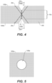
- FIGS. 4 and 5 illustrate an example of a first via-formation state of the inorganic substrate 100 subjected to the DSOP according to some embodiments of block 204 in FIG. 2 .
- the first via-formation state is an interim via-formation state at a time during but before completion of the DSOP, according to some embodiments.
- the wet etch of the DSOP is isotropic and causes, as illustrated by a comparison of FIGS. 3 and 4 , the diameter of an opening at each end of the damage track 10 to grow as the etch depth increases along the line of the damage track 10.
- the longitudinal axis 32 bisects a width of the via or pathway (e.g., via or pathway 30 or resultant via or pathway 30a discussed in more detail below) at least at one or both of the openings of the via or pathway in the first surface 100a and second surface 100b of the inorganic substrate 100.
- the longitudinal axis 32 proceeds through a center of a lateral cross section of either or both of the openings (e.g., openings 106a2, 106b2 in the example of FIG. 6B ) in surfaces 100a, 100b, the lateral cross section(s) residing within the plane(s) (e.g., first plane 102a, second plane 102b, or both) of the respective opening(s).
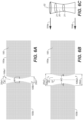
- FIG. 6A may result in a via or pathway 30 in the state of FIG. 6B , which illustrates a larger via or pathway 30 compared to FIG. 6A , due to the longer wet etching process associated with FIG. 6B , according to some embodiments.
- the waist of the via or pathway 30 may be determined as the location along the longitudinal axis 32 of the via or pathway 30 having the smallest lateral two-dimensional cross-sectional area, according to some embodiments.
- all diameters may be required to extend in the same directions or reside within a same plane taken along the longitudinal axis 32 (e.g., a profile of the via or pathway 30 that is perpendicular to the lateral cross-sections of the via or pathway 30), according to some embodiments.
- a method of facilitating formation of a via in an inorganic substrate may include (e.g., according to block 204 in FIG. 2 ), applying the DSOP to the inorganic substrate 100, the inorganic substrate 100 including a damage track 10 having a first end 10a in a first surface 100a of the inorganic substrate 100 and a second end 10b in a second surface 100b of the inorganic substrate 100.
- the second surface 100b is on an opposite side of the inorganic substrate 100 than the first surface 100a of the inorganic substrate 100.
- the DSOP may enlarge at least a first dimension (e.g., a size, diameter, or area of lateral cross-section) of the second end 10b of the damage track 10 to form a first opening (e.g., first opening 106b2) in the second surface 100b of the inorganic substrate 100.
- the first dimension of the second end 10b of the damage track 10 may be measured within a plane (e.g., plane 102b) of the second surface 100b of the inorganic substrate 100.
- the DSOP produces a via or pathway 30 extending between the first opening (e.g., first opening 106a2) in the first surface 100a of the inorganic substrate 100 and the first opening (e.g., first opening 106b2) in the second surface 100b of the inorganic substrate 100.
- the via or pathway 30 may include a longitudinal axis 32 perpendicular to (a) an extension direction (e.g., extension direction 104a) of the first surface 100a of the inorganic substrate 100, (b) an extension direction (e.g., extension direction 104b) of the second surface 100b of the inorganic substrate 100, or both (a) and (b).
- the via or pathway 30 may include varying diameters of lateral cross-sections (e.g., cross-sections 31) taken perpendicular to the longitudinal axis 32 of the via or pathway 30, according to some embodiments.
- the pathway includes a waist coinciding with a lateral cross-section of the via or pathway 30 taken perpendicular to the longitudinal axis 32 at a point of minimum diameter of the varying diameters of the pathway
- the DSOP may be any process that etches or removes portions of the inorganic substrate 100 preferentially in the location of the damage track 10 from both sides of the inorganic substrate 100 so as to enlarge the damage track 10 to form a partial or fully formed via (e.g., akin to FIGS. 4 , 6A, and 6B , depending on desired via shaping, according to some embodiments).
- the DSOP may include etching with reactive gases in a configuration that gives access to both surfaces 100a, 100b, and immersive wet processes involving acidic or basic solutions. Immersive wet processes may be preferred in various contexts. An immersive double-sided opening process performed in a tank may be particularly suitable in various contexts.
- the immersive wet process may also include agitation of the solution in the tank.
- Agitation may include fluid flow, application of ultrasonic energy in the range of 30kHz to approximately 1MHz, or application of so called megasonic mixing involving the application of frequencies near and above 1MHz.
- Etching may be accomplished with solutions of hydroxides, including but not limited to potassium hydroxide, sodium hydroxide, and tetramethylammonium hydroxide at temperatures above 50° C, preferably above 75° C.
- solutions containing hydrogen fluoride (HF) may be preferable.
- Solution compositions including HF at concentrations from 0.1 to 10M may be preferable, and may include additional components to lower or raise pH.
- the additional components may include, but are not limited to, hydrochloric acid, nitric acid, and ammonium fluoride, according to various embodiments. Additional components may include surfactants. Temperature of the tank may be as cold as - 10° C or up to 60° C, with a range between 0° C and 50° C being preferable in some contexts.
- Additives that modify the shape of the via formed during the DSOP may be used.
- additives that promote the formation of a via with a waist diameter that is closest to the diameter of the top opening or bottom opening may be used.
- additives that produce a via shape with the minimum variation of via diameter across the thickness of the substrate, or produce a via with a shape closest to cylindrical may be used.
- Such additives may include any additives that reduce the surface etch rate of a particular etchant, while minimally affecting the diffusion rates of the etchant, may be used, according to some embodiments.
- Multicomponent glasses such as borosilicate or aluminoborosilicate glass contain components such as calcium and magnesium that tend to precipitate upon etching with HF. This precipitation may lead to non-uniform etch and fouling of the etching vessels.
- Certain etchant formulations prevent significant precipitation, generally by providing lower hydrofluoric concentration and higher concentrations of a strong acid.
- a strong acid may be any acid with an acid dissociation constant, pKa, of less than 2, preferably less than 1 in some contexts, including but no limited to hydrochloric, nitric, or sulfuric acid.
- Preferred etching solutions may contain an HF concentration less than between 0.1 and 1M and a strong acid concentration greater than 0.8M and less than 10M, preferably less than 5M in some contexts.
- Particularly preferred etching compositions may contain an HF concentration below 0.6M and a strong acid concentration above 1M.
- the DSOP need not produce a complete via opening that progresses all the way through the inorganic substrate 100, as shown, e.g., by the state of FIG. 4 , where the opening 106a and the opening 106b exist, but a region of the damage track 10 corresponding to length 10s in FIG. 4 exists between the openings 106a, 106b. In some embodiments where the DSOP completes in the via-formation state of FIG.
- a pathway extends from or between the opening 106a (an example of a first opening in the first surface 100a of the inorganic substrate 100 in this example) to or and the opening 106b (an example of a first opening in the second surface 100b of the substrate 100 in this example), such that the pathway includes the remaining portion of the damage track 10 corresponding to length 10s.
- the progression of the complete via opening through the entirety of the inorganic substrate 100 may be completed by a single-sided opening process, discussed in more detail below with respect to at least block 208 in FIG. 2 .
- the DSOP completes in the via-formation state of FIG.
- the etch is allowed to proceed until the 'top' (surface 100a) and 'bottom' (surface 100b) opening diameters, which are generally comparable, have enlarged to within 30%, or more preferably in some contexts within 20%, or more preferably still in some contexts within 10% of the desired final opening size of the via or pathway 30 at surface 100b, according to some embodiments.
- a diameter (e.g., diameter 20b in FIG. 4 , diameter 20b1 in FIG. 6A , or diameter 20b2 in FIG. 6B ) of the first opening (e.g., first opening 106b in FIG. 4 , first opening 106b1 in FIG. 6A , or first opening 106b2 in FIG. 6B ) in the second surface 100b of the inorganic substrate 100 is within 20% in some embodiments, or within 10% in some embodiments, of a corresponding diameter (e.g., diameter 20b3 in FIG. 7A , diameter 20b4 in FIG. 7B , or diameter 20b5 in FIG. 7C ) of the second opening (e.g., second opening 106b3 in FIG.
- opening 106b4 in FIG. 7B , or opening 106b5 in FIG. 7C in the second surface 100b of the inorganic substrate 100, the diameter of the first opening in the second surface 100b of the inorganic substrate 100 and the corresponding diameter of the second opening in the second surface 100b of the inorganic substrate 100 are measured along parallel line segments.
- the waist position is at or substantially at the center of the substrate (along its thickness dimension) as measured along the longitudinal axis 32, according to some embodiments.
- the ratio of the waist diameter to the diameter of either of the opening diameters of the openings in surfaces 100a, 100b of the via or pathway 30 is less than 1, according to some embodiments, indicating that the waist diameter is smaller than the opening diameters.
- the conical shape proceeding from the resulting openings in surfaces 100a, 100b may have smaller diameters occurring at some point along the longitudinal axis 32 than the diameters of either of the openings at their respective surfaces 100a, 100b.
- the resulting shape of the via or pathway 30 upon completion of the DSOP may be an hourglass shape, e.g., as shown in FIG. 6A and FIG. 6B , according to some embodiments.
- the ratio of the waist diameter to the opening diameters upon completion of the DSOP be greater than 0.5, or preferably greater than 0.7, according to various embodiments.
- the position of the waist of the via or pathway 30 may occur at any point between the first surface 100a and the second surface 100b, according to various embodiments. Generally, the waist occurs near the midpoint of the inorganic substrate 100 between the first surface 100a and the second surface 100b upon conclusion of the DSOP.
- the discussions herein commonly refer to consistent references for the first surface 100a, the second surface 100b, and the thickness 110 of the inorganic substrate 100 for purposes of clarity and ease of explanation
- the first surface 100a, the second surface 100b, and the thickness 110 change during the DSOP or any process that etches away at the substrate, as etching may reduce the thickness of the inorganic substrate 100 as a function of the duration of the application of the etch.
- a midpoint of the thickness and the like of the inorganic substrate 100 such a midpoint and the like may be determined according to the thickness of the inorganic substrate 100 existing at the time of midpoint measurement, according to some embodiments.
- the waist of the via or pathway 30 may exist between 30% and 70% of the distance between the first surface 100a and the second surface 100b.
- the waist preferably may exist between 40% and 60% of the distance between the first surface 100a and the second surface 100b, according to some embodiments.
- surface 100b of the inorganic substrate 100 may be protected, sealed, or blocked, in preparation for application of a single-sided opening process ("SSOP").
- SSOP single-sided opening process
- the SSOP may include a wet etching process applied to the first surface 100a of the inorganic substrate 100, but not to the second surface 100b of the inorganic substrate.
- second surface 100b may be protected, sealed, or blocked by applying an adhesive etch-resistant film on second surface 100b, according to some embodiments.
- Second surface 100b may also be protected, sealed, or blocked by temporarily bonding a carrier or blocking substrate, preferably an etch-resistant carrier or blocking substrate, to second surface 100b, according to some embodiments.
- a carrier or blocking substrate preferably an etch-resistant carrier or blocking substrate
- the temporary bond adhesive is polymeric, the polymer can wick into the via 30 formed in the DSOP and may adversely affect the SSOP. Accordingly, it may be preferable in some applications to protect, seal, or block second surface 100b by temporarily bonding a carrier or blocking substrate with a carbonaceous surface modification layer applied, according to some embodiments.
- a carrier or blocking substrate preferably an etch-resistant carrier or blocking substrate
- an inorganic carbon-containing film may be deposited on a surface of a carrier or blocking substrate, and the inorganic carbon-containing film may be bonded to the second surface 100b of the inorganic substrate 100.
- the carrier or blocking substrate may be any substrate with sufficient mechanical properties and smoothness to adhere to the inorganic substrate 100 and protect, seal, or block penetration of etchant solution, and not be overly reactive to the etchant solution, according to some embodiments.
- Suitable carrier or blocking substrates that may be bonded to the second surface 100b of the inorganic substrate 100 after completion of the DSOP, but before applying the SSOP, include semiconductor substrates, including but not limited to, silicon and germanium, according to some embodiments.
- semiconductor substrates including but not limited to, silicon and germanium, according to some embodiments.
- the second surface 100b of the inorganic substrate 100 is temporarily bonded to a semiconductor substrate using a deposited carbonaceous layer.
- the semiconductor substrate may be made of silicon.
- Carbonaceous surface modification layers allow a higher adhesion force between the second surface 100b and the carrier or blocking substrate than simple Van der Waals interactions between the clean surfaces, yet remain temporary even after anneals to 400° C.
- Carbonaceous surface modification layers may include one or more layers or films which contain carbon as a significant component.
- the carbon may exist in the form of polymeric chains exhibiting finite molecular weight.
- the carbon may exist as a matrix of carbon atoms bonded to form an amorphous or crystalline solid film.
- the carbon may exhibit sp 2 bonding or sp 3 bonding, also referred to as sp 2 or sp 3 orbital hybridization.
- the carbonaceous surface modification layers may contain substantial quantities of other atoms.
- Preferred additional atoms may include hydrogen and fluorine, at concentrations below 50 atomic % relative to the entire film, or preferably below 40 atomic % relative to the entire film, according to various embodiments.
- Preferred carbonaceous surface modification layers may be amorphous carbon, amorphous hydrogenated carbon, diamond, diamond-like carbon, and fluorine containing carbon films, according to various embodiments.
- the carbonaceous surface modification layers may be deposited by any suitable deposition technique, according to some embodiments.
- Preferred deposition techniques may include vacuum deposition, preferably plasma enhanced chemical vapor deposition (PECVD), according to various embodiments.
- a particularly preferred deposition technique may be PECVD in the presence of a voltage-floating platen as used in reactive ion etch (RIE) systems, according to some embodiments.
- the carbonaceous surface modification layers may be of any desired thickness. Layer thickness below 100 nm may be preferred, according to some embodiments, and a particularly preferred layer thickness may be below 50 nm, according to some embodiments.
- the carbonaceous surface modification layers may include an exposed surface with very low roughness. The roughness of the surface may be below 10 nm, preferably below 1nm in RMS roughness, according to some embodiments.
- the carbonaceous surface modification layers may be applied to either or both surfaces that are to be bonded.
- the carbonaceous surface modification layers may be applied either to the surface of the glass substrate or to the surface of a silicon substrate that are to be bonded, or to both of the surfaces to be bonded.
- the surfaces to be bonded are the two surfaces from different substrates that are contacted during bonding, as opposed the two opposing surfaces of single substrate, according to some embodiments.
- the bonding or bonding type between the inorganic substrate 100 and the carrier or blocking substrate may be of any type that permits the two substrates to remain in adhesion during all envisioned processing steps of at least the SSOP (e.g., according to block 208 in FIG. 2 ), but allows debonding without excessive force when required, according to some embodiments.
- a preferred method of bonding may be Van der Waals bonding, in which the substrates are held together due to Van der Waals forces resulting from atomic constituents present on the two surfaces (e.g., surface 100b of the inorganic substrate 100 and the surface of the carrier or blocking substrate) being bonded.
- Van der Waals forces may result in bonded substrates with bond energies ranging from 20 to 300 mJ/m 2 as measured by a razor insertion technique (see, e.g., Gillis, Peter P., et al., "Double-Cantilever Cleavage Mode of Crack Propagation", Journal of Applied Physics 35, 647 (1964 )).
- Van der Waals bonds may be modified by treating surfaces to be bonded with processes including, but not limited to, cleaning, acid exposure, base exposure, plasma treatments, and ozone treatments, according to various embodiments.
- the bonding or bonding type may also include some number of covalent bonds that form at room temperature or above and serve to covalently connect moieties on the two respective surfaces.
- the starting roughness, details of the DSOP etchant solution composition, conditions of the etch bath including agitation and temperature, and time in the solution determine the roughness of the substrate surfaces after the etch, according to some embodiments.
- the roughness may be dramatically increased, essentially maintained, or in some cases decreased after the DSOP.
- Another advantage of applying the DSOP according to block 204 in FIG. 2 followed by the SSOP according to block 206 in FIG. 2 is that the resulting shape of the via lends itself to ready filling with electrically conductive material in subsequent processes.
- a via profile that does not contain a re-entrant portion may be preferred for single-side via filling.
- superimposing an etching process that tends to create a conical profile (SSOP) onto an hour-glass via profile would not create a useful profile without reentrance.
- etching condition for the DSOP by careful choice for the etching condition for the DSOP and then carefully tuning the etching conditions (e.g., choosing conditions distinctly optimized away from the conditions chosen for the DSOP) for the SSOP, it is possible to create a via profile without significant reentrance.
- a method of facilitating formation of a via in an inorganic substrate may include (e.g., according to block 208 in FIG. 2 ) applying the SSOP to the first surface 100a of the inorganic substrate 100, after completion of the DSOP associated with block 204 in FIG. 2 .
- the SSOP may enlarge at least a first dimension (e.g., diameter 20a in FIG. 4 , diameter 20a1 in FIG. 6A , or diameter 20a2 in FIG. 6B ) of the first opening (e.g., opening 106a in FIG. 4 , opening 106a1 in FIG. 6A , or opening 106a2 in FIG.
- the SSOP moves the waist of the via or pathway 30 closer to the second surface 100b of the inorganic substrate 100 as compared to a location of the waist after completion of the DSOP but before applying the SSOP, e.g., as illustrated by a comparison of at least (a) FIG. 6A or FIG. 6B with (b) FIG. 7A, FIG. 7B, or FIG. 7C .
- the moving of the waist may be considered to form a resultant via or pathway (e.g., resultant via or pathway 30a illustrated in FIGS. 7 ).
- the SSOP causes a via (e.g., at least resultant via or pathway 30a) formed in the inorganic substrate 100 to include the second opening (e.g., opening 106a3 in FIG. 7A , opening 106a4 in FIG. 7B , or opening 106a5 in FIG. 7C ) in the first surface 100a of the inorganic substrate, a resultant second opening (e.g., opening 106b3 in FIG. 7A , opening 106b4 in FIG. 7B , or opening 106b5 in FIG.
- the second opening e.g., opening 106a3 in FIG. 7A , opening 106a4 in FIG. 7B , or opening 106b5 in FIG.
- the resultant pathway 30a extending from the second opening (e.g., opening 106a3 in FIG. 7A , opening 106a4 in FIG. 7B , or opening 106a5 in FIG. 7C ) in the first surface 100a of the inorganic substrate 100 to the resultant second opening (e.g., opening 106b3 in FIG. 7A , opening 106b4 in FIG. 7B , or opening 106b5 in FIG. 7C ) in the second surface 100b of the inorganic substrate 100, according to some embodiments.
- the resultant second opening e.g., opening 106b3 in FIG.
- opening 106b4 in FIG. 7B , or opening 106b5 in FIG. 7C in the second surface 100b of the inorganic substrate 100 is the original first opening (e.g., opening 106b in FIG. 4 , opening 106b1 in FIG. 6A , or opening 106b2 in FIG. 6B ) in the second surface 100b of the inorganic substrate 100, subject to any effects on such original first opening due to the application of the SSOP, which, in some embodiments, is nil or relatively minimal.
- the resultant second opening e.g., opening 106b3 in FIG. 7A , opening 106b4 in FIG. 7B , or opening 106b5 in FIG.
- the position of the waist (e.g., waist W3 in FIG. 7A , waist W4 in FIG. 7B , or waist W5 in FIG. 7C ), is preferably within 10% of the total thickness (remaining) of the inorganic substrate 100 from the second surface 100b of the inorganic substrate 100.
- the SSOP applied to the first surface 100a of the inorganic substrate 100 may result in a funnel-shaped, trumped-shaped, megaphone-shaped, frustum-shaped, or conical frustum-shaped resultant via or pathway 30a.
- FIG. 7A-7C such as FIG. 7A
- the resultant via or pathway 30a may be funnel-shaped, where the internal diameters of the resultant via or pathway 30a taken in a sequence of lateral cross-sections perpendicular to longitudinal axis 32 are consistent or relatively consistent over a length of the longitudinal axis 32 adjacent the blocked or sealed second surface 100b, at a value smaller than the diameter in the upper section (toward surface 100a) of the resultant via or pathway 30a.
- the region of the resultant via or pathway 30a adjacent the blocked or sealed second surface 100b, where the lateral cross-sections perpendicular to longitudinal axis 32 are consistent or relatively consistent, represents the smallest or approximately the smallest diameter or diameters of the resultant via or pathway 30a taken within one or more lateral cross-sections perpendicular to longitudinal axis 32.
- the SSOP moves the waist of the resultant via or pathway 30a closer to the second surface 100b of the inorganic substrate 100 as compared to a location of the waist after completion of the DSOP but before applying the SSOP, e.g., as illustrated by a comparison of at least (a) FIG. 6A or FIG. 6B with (b) FIG. 7A, FIG. 7B, or FIG.
- the waist may be considered to apply to a region (rather than just a point) of minimum or near minimum internal diameter(s) of the resultant via or pathway 30a, as illustrated, e.g., by waist W5 in FIG. 7C .
- the size (e.g., diameter or area) of the opening in the first surface 100a, exposed directly to the etching solution expands more than the other portions of the via or pathway.
- the diameter (e.g., diameter 20a3 in FIG. 7A or diameter 20a4 in FIG. 7B ) of the second opening (e.g., opening 106a3 in FIG. 7A or opening 106a4 in FIG. 7B ) in the second surface 100b of the inorganic substrate 100 is in a range of 1.2 to 3 in some embodiments, in a range of 1.4 to 3 in some embodiments, in a range of 1.4 to 2 in some embodiments, and in a range of 1.2 to 2 in some embodiments.
- the diameter of the second opening in the first surface 100a of the inorganic substrate 100 and the corresponding diameter of the resultant second opening in the second surface 100b of the inorganic substrate 100 are measured along parallel line segments, according to some embodiments.
- a preferred shape of the resultant via or pathway 30a may be any shape in which the diameter of the resultant via or pathway 30a is decreasing, constant, or only minimally increasing in moving along the longitudinal axis 32 of the resultant via or pathway 30a from the first surface 100a (or at least the first plane 102a in which the first surface 100a resides) of the inorganic substrate 100 to the second surface 100b (or at least the second plane 102b in which the second surface 100b resides) of the inorganic substrate 100.
- the openings of the resultant via or pathway 30a in the first surface 100a and the second surface 100b may have a circular shape.
- a cross-section of the second opening e.g., opening 106a3 in FIG. 7A , opening 106a4 in FIG. 7B , or opening 106a5 in FIG.
- a longitudinal axis (e.g., longitudinal axis 32) of the resultant via or pathway 30a may have a circular shape, the longitudinal axis of the resultant via or pathway 30a perpendicular to, e.g., (a) an extension direction (e.g., extension direction 104a) of the first surface 100a of the inorganic substrate 100, (b) an extension direction (e.g., extension direction 104b) of the second surface 100b of the inorganic substrate 100, or both (a) and (b).
- a cross-section of the resultant second opening e.g., opening 106b3 in FIG.
- opening 106b4 in FIG. 7B , or opening 106b5 in FIG. 7C ) in the second surface 100b of the inorganic substrate 100, taken perpendicular to a longitudinal axis (e.g., longitudinal axis 32) of the resultant via or pathway 30a, may have a circular shape.
- the longitudinal cross-section or profile of the resultant via or pathway 30a taken along the longitudinal axis 32 (i.e., within a plane in which the longitudinal axis 32 resides), may have substantially linear walls, which leads to a frustum or conical frustum shape of the resultant via or pathway 30a.
- a conical frustum may be defined as the shape produced when a cone, which has a base and a point or tip, is cut off by two planes parallel to the base, such that at least the point or tip is removed.
- the longitudinal cross-section or profile of the resultant via or pathway 30a may have curved walls.
- each curved wall has a lower angle between it and the plane (e.g., plane 102a) in which the first surface 100a resides taken in a direction toward an interior of the resultant via or pathway 30a than the curved wall has between it and the plane (e.g., plane 102b) in which the second surface 100b resides taken in a direction toward an interior of the resultant via or pathway 30a, as shown in the example of FIG. 7B , according to some embodiments.
- Such a configuration leads to a trumpet shape of the resultant via or pathway 30a, in which the diameters of the lateral cross-sections (akin to lateral cross-sections 31) of the resultant via or pathway 30a as one progresses along the longitudinal axis 32 from the first surface 100a (or at least the first plane 102a in which the first surface 100a resides) to the second surface 100b (or at least the second plane 102b in which the second surface 100b resides) decrease more rapidly near the first surface 100a than near the second surface 100b.
- the frustum or trumpet shapes are a direct consequent of the SSOP, in which etching reactants have more access to portions of the opening near the first surface 100a than they do near the second surface 100b as a result of the blocked access at the second surface 100b described above with respect to block 206 in FIG. 2 .
- a first angle ⁇ of a first portion 108a of a wall 108 of the resultant via or pathway 30a at or adjacent the second opening 106a5 in the first surface 100a of the inorganic substrate 100 is at least two (2) degrees, in some embodiments, and preferably at least four (4) degrees in some embodiments, greater than a second angle ⁇ of a second portion 108b of the wall 108 of the resultant via or pathway 30a at or adjacent the resultant second opening 106b5 in the second surface 100b of the inorganic substrate 100, each of the first angle ⁇ and the second angle ⁇ being taken between (i) the first portion 108a or the second portion 108b, respectively, of the wall 108 of the resultant via or pathway 30a, and (ii) the longitudinal
- the first angle ⁇ of the first portion 108a of the wall 108 of the resultant via or pathway 30a at or adjacent the second opening 106a5 in the first surface 100a of the inorganic substrate 100 is between two (2) to eight (8) degrees (inclusive), in some embodiments, and between four (4) to eight (8) degrees (inclusive), in some embodiments, greater than the second angle ⁇ of a second portion 108b of the wall 108 of the resultant via or pathway 30a at or adjacent the resultant second opening 106b5 in the second surface 100b of the inorganic substrate 100.
- the first portion 108a is a span (e.g., the longest span in some embodiments) of the wall 108 between the first surface 100a and at least a portion (e.g., an initial portion 108a1 in some embodiments) of the waist (e.g., waist W5 in the example of FIG. 7C ) closest to the first surface 100a in which the angle or slope of the wall is constant or substantially constant.
- a span e.g., the longest span in some embodiments
- the waist e.g., waist W5 in the example of FIG. 7C
- the second portion 108b is a span (e.g., the longest span in some embodiments) of the wall 108 between the second surface 100b and the at least the portion (e.g., the initial portion 108a1 in some embodiments) of the waist (e.g., waist W5 in the example of FIG. 7C ) closest to the first surface 100a in which the angle or slope of the wall is constant or substantially constant.
- the first portion 108a and the second portion 108b of the wall 108 which portions 108a, 108b are used to determine the first angle ⁇ and the second angle ⁇ , according to some embodiments, may be selected from respective regions of the wall 108 that are separated by a point of inflection (e.g., portion 108a1 in the example of FIG. 7C ) in the angle or slope of the wall 108, such as may be present at the waist of the resultant via or pathway 30a.
- the diameter of the second opening on the second surface 100b may be slightly larger than the waist, as exemplified in FIG. 7A with opening 106b3 having a diameter 20b3. In this case, a similar span to 108b from FIG. 7C would exhibit a negative angle ⁇ .
- the SSOP moves the waist of the resultant via or pathway 30a closer to the blocked second surface 100b, as can be seen by comparing FIG. 4 , FIG. 6A, or FIG. 6B to FIG. 7C .
- the wet-etch fluid used for the SSOP also performs a lateral etch, shown by undercut region 65, at the interface between the surface 100b and the adhered surface of the protectant 70.
- the lateral etch can result from etch acceleration at the interface between blocked second surface 100b of inorganic substrate 100 and protectant 70.
- the extent of lateral etch can be limited relative to, for example, the case of not performing the DSOP and attempting to perform only a single sided etch on a substrate with a protectant, because in the case having first performed the DSOP, the first opening (e.g., at least first opening 106b2 in FIG. 6B , among others) in the second surface 100b is already fairly close in diameter to the diameter of the desired second opening (e.g., second opening 106b5 in FIG. 7C ) in the second surface 100b, so the time the substrate spends in the wet-etch fluid for the SSOP may be determined by the time taken to move the waist W of the via or pathway closer to the second surface 100b of the inorganic substrate 100.
- the first opening e.g., at least first opening 106b2 in FIG. 6B , among others
- the desired second opening e.g., second opening 106b5 in FIG. 7C
- the lateral extent of the lateral etching (shown by diameter 60 in FIG. 7C ), also referred to as undercutting, can be larger than the diameter 20b5 of the second opening 106b5 at the second surface 100b and can be larger than the diameter 20a5 of the second opening 106a5 at the first surface 100a.
- the waist W5 in the example of FIG. 7C of the resultant via or pathway 30a may have the same or substantially a same diameter over a distance along the longitudinal axis 32 in the resultant via or pathway 30a, forming a cylindrical section corresponding to the region of waist W5 extending to the second opening 106b5 close to the interface of the second surface 100b of the inorganic substrate 100 with the protectant layer 70.
- the undercut region (e.g., region 65 of lateral etch in FIG. 7C ) may be considered to not be part of the resultant via or pathway 30a, according to some embodiments.
- the distance 65a from the protectant 70 to the smallest diameter of the resultant via or pathway 30a is less than 10% in some embodiments, or less than 5% in some embodiments, of the etched substrate thickness (e.g., thickness 110a in FIG. 7C )
- the undercut region (e.g., region 65 of lateral etch in FIG.
- undercutting may be considered to be a footer rather than part of the resultant via or pathway 30a, and the diameter (e.g., diameter 20b5) is considered to be the diameter of the second opening 106b5 in second surface 100b of the inorganic substrate 100.
- this interpretation is also illustrated by the representation that the second surface 100b of the inorganic substrate 100 includes a surface of the undercut region (e.g., region 65 of lateral etch in FIG. 7C ) on the inorganic substrate 100.
- the undercut region e.g., region 65 of lateral etch in FIG. 7C
- the resultant via or pathway 30a may still be considered to be tapered, but to also comprise a footer or undercut region (e.g., region 65 of lateral etch in FIG. 7C ).
- the resultant via or pathway 30a may be considered to be one with a waist and not a tapered through-hole, according to some embodiments.
- the diameter 60 of the undercut region (e.g., region 65 of lateral etch in FIG. 7C ) may be produced to be as small as possible, according to some embodiments.
- the diameter 60 of undercut region (e.g., region 65 of lateral etch in FIG. 7C ) may be less than four times the diameter 20b5 of the second opening 106b5 in the second surface 100b in some embodiments, and preferably less than three times the diameter 20b5 of the second opening 106b5 in the second surface 100b of the inorganic substrate 100, according to some embodiments.
- a method of facilitating formation of a via in an inorganic substrate may include (e.g., according to block 208 in FIG. 2 ) applying a SSOP to the first surface 100a of the inorganic substrate 100, after bonding a carrier or blocking semiconductor substrate to the second surface 100b of the inorganic substrate 100 (e.g., according to block 206 in FIG. 2 ).
- the SSOP may enlarge at least a first dimension (e.g., diameter 20a in FIG. 4 , diameter 20a1 in FIG. 6A , or diameter 20a2 in FIG. 6B ) of the first opening (e.g., opening 106a in FIG. 4 , opening 106a1 in FIG.
- the SSOP may cause the resultant via or pathway 30a to include the second opening in the first surface 100a of the inorganic substrate 100 and a resultant second opening (e.g., opening 106b3 in FIG. 7A , opening 106b4 in FIG. 7B , or opening 106b5 in FIG.
- a useful via with a trumpet shape was produced by a combination of a double-sided opening process followed by a single-sided opening process according an embodiment of the present invention.
- the resulting glass was cleaned with a plasma treatment and then received a carbonaceous layer as described above.
- the resulting glass was then bonded to a silicon wafer on which a carbonaceous layer was also deposited.
- the bonding is a spontaneous process in which the two samples are brought into contact and the bond progresses between the two substrates.
- the resulting bonded pair was etched in a solution 0.4M HF and 1.8M HCl, maintained at approximately 40° C, for 40 minutes with light megasonics agitation. Due to the blocking of one side of the substrate with the silicon wafer, the etching occurs predominantly on the other side of the glass substrate.
- the resulting via is shown in SEM cross section in FIG. 8 , with the darker region representing the interior of the via (filled with polymer for the SEM cross section process).
- the top diameter of the via is approximately 32 microns, while the bottom diameter of the via is 19 microns.
- the via has a trumpet shape with little to no reentrancy, and is suitable for typical via fill / metallization plating approaches.
Landscapes
- Engineering & Computer Science (AREA)
- Physics & Mathematics (AREA)
- Chemical & Material Sciences (AREA)
- Optics & Photonics (AREA)
- General Chemical & Material Sciences (AREA)
- Chemical Kinetics & Catalysis (AREA)
- Plasma & Fusion (AREA)
- Mechanical Engineering (AREA)
- Geochemistry & Mineralogy (AREA)
- Materials Engineering (AREA)
- Organic Chemistry (AREA)
- Life Sciences & Earth Sciences (AREA)
- Health & Medical Sciences (AREA)
- Toxicology (AREA)
- Oil, Petroleum & Natural Gas (AREA)
- Internal Circuitry In Semiconductor Integrated Circuit Devices (AREA)
- Ceramic Engineering (AREA)
- Drying Of Semiconductors (AREA)
Claims (16)
- Procédé facilitant la formation d'un trou d'interconnexion dans un substrat inorganique (100), le procédé comprenant :l'application (204) d'un processus d'ouverture double face au substrat inorganique, le substrat inorganique comprenant une piste d'endommagement (10) ayant une première extrémité (10a) dans une première surface (100a) du substrat inorganique et une seconde extrémité (10b) dans une seconde surface (100b) du substrat inorganique, la seconde surface étant sur un côté opposé du substrat inorganique par rapport à la première surface du substrat inorganique, le processus d'ouverture double face agrandissant au moins une première dimension de la première extrémité de la piste d'endommagement pour former une première ouverture (106a) dans la première surface du substrat inorganique, la première dimension de la première extrémité de la piste d'endommagement étant mesurée dans un plan (102a) de la première surface du substrat inorganique, et le processus d'ouverture double face agrandissant au moins une première dimension de la seconde extrémité de la piste d'endommagement pour former une première ouverture (106b) dans la seconde surface du substrat inorganique, la première dimension de la seconde extrémité de la piste d'endommagement étant mesurée dans un plan (102b) de la seconde surface du substrat inorganique, un passage (30) s'étendant entre la première ouverture dans la première surface du substrat inorganique et la première ouverture dans la seconde surface du substrat inorganique, le passage comprenant un axe longitudinal (32) perpendiculaire à (a) une direction d'extension (104a) de la première surface du substrat inorganique, (b) une direction d'extension (104b) de la seconde surface du substrat inorganique, ou à la fois (a) et (b), le passage comprenant des diamètres variables de sections transversales latérales prises perpendiculairement à l'axe longitudinal du passage, le passage comprenant une taille (W1) coïncidant avec une section transversale latérale (31) du passage prise perpendiculairement à l'axe longitudinal en un point de diamètre minimum des diamètres variables du passage ; etl'application (208) d'un processus d'ouverture d'un seul côté à la première surface du substrat inorganique, après l'achèvement du processus d'ouverture double face, le processus d'ouverture d'un seul côté agrandissant au moins une première dimension (20a) de la première ouverture dans la première surface du substrat inorganique pour former une seconde ouverture (106a3) dans la première surface du substrat inorganique, le processus d'agrandissement d'ouverture d'un seul côté déplaçant la taille du passage plus près de la seconde surface du substrat inorganique par rapport à un emplacement de la taille après l'achèvement du processus d'ouverture double face mais avant l'application du processus d'ouverture d'un seul côté, le déplacement de la taille formant un passage résultant, le processus d'ouverture d'un seul côté amenant un trou d'interconnexion formé dans le substrat inorganique à comprendre la seconde ouverture dans la première surface du substrat inorganique, une seconde ouverture résultante (106b3) dans la seconde surface du substrat inorganique, et le passage résultant (30a), le passage résultant s'étendant depuis la seconde ouverture dans la première surface du substrat inorganique jusqu'à la seconde ouverture résultante dans la seconde surface du substrat inorganique.
- Procédé selon la revendication 1, dans lequel le processus d'ouverture double face comprend un processus de gravure humide appliqué simultanément à la première surface (100a) du substrat inorganique (100) et à la seconde surface (100b) du substrat inorganique.
- Procédé selon la revendication 1, dans lequel le processus d'ouverture d'un seul côté comprend un processus de gravure humide appliqué à la première surface (100a) du substrat inorganique (100), mais pas à la seconde surface (100b) du substrat inorganique.
- Procédé selon la revendication 1, dans lequel le substrat inorganique (100) est du verre.
- Procédé selon la revendication 1,dans lequel un rapport entre (a) un diamètre (20a3) de la seconde ouverture (106a3) dans la première surface (100a) du substrat inorganique (100) et (b) un diamètre (20b3) de la seconde ouverture résultante (106b3) dans la seconde surface (100b) du substrat inorganique est compris entre 1,2 et 3, etdans lequel le diamètre de la seconde ouverture dans la première surface du substrat inorganique et le diamètre de la seconde ouverture résultante dans la seconde surface (100b) du substrat inorganique sont mesurés le long de segments de ligne parallèles.
- Procédé selon la revendication 1,dans lequel un rapport entre (a) un diamètre (20a3) de la seconde ouverture (106a3) dans la première surface (100a) du substrat inorganique (100) et (b) un diamètre de la taille (W1) du passage résultant (30a) à l'issue du processus d'ouverture d'un seul côté est compris entre 1,2 et 3, etdans lequel le diamètre de la seconde ouverture dans la première surface du substrat inorganique et le diamètre de la taille du passage résultant sont mesurés le long de segments de ligne parallèles.
- Procédé selon la revendication 1,dans lequel un diamètre (20b) de la première ouverture (106b) dans la seconde surface (100b) du substrat inorganique (100) est à moins de 20 % d'un diamètre correspondant (20b3) de la seconde ouverture résultante (106b3) dans la seconde surface du substrat inorganique, etdans lequel le diamètre de la première ouverture dans la seconde surface du substrat inorganique et le diamètre correspondant de la seconde ouverture résultante dans la seconde surface du substrat inorganique sont mesurés le long de segments de ligne parallèles.
- Procédé selon la revendication 1, dans lequel, à l'issue du processus d'ouverture d'un seul côté, le passage résultant (30a) présente une forme de trompette ou une forme tronconique.
- Procédé selon la revendication 1, comprenant la liaison d'un substrat semi-conducteur à la seconde surface (100b) du substrat inorganique (100) après achèvement du processus d'ouverture double face, mais avant l'application du processus d'ouverture d'un seul côté.
- Procédé selon la revendication 9, dans lequel la liaison est une liaison de Van der Waals ou une liaison de Van der Waals assistée par liaison covalente.
- Procédé selon la revendication 1, comprenant la liaison temporaire du substrat inorganique (100) à un substrat semi-conducteur à l'aide d'une couche carbonée déposée.
- Procédé selon la revendication 11, dans lequel la couche carbonée déposée comprend un carbone amorphe, un carbone hydrogéné amorphe, un diamant, un carbone de type diamant ou un film de carbone contenant du fluor.
- Procédé selon la revendication 1, comprenant, après l'achèvement du processus d'ouverture double face, mais avant l'application du processus d'ouverture d'un seul côté, le dépôt d'un film contenant du carbone inorganique sur une surface d'un substrat de blocage et la liaison du film contenant du carbone inorganique à la seconde surface (100b) du substrat inorganique (100).
- Procédé selon la revendication 1, dans lequel le processus d'ouverture double face produit un trou d'interconnexion à travers le substrat inorganique (100) à partir de la piste endommagée (10).
- Procédé selon la revendication 1, dans lequel le processus d'ouverture d'un seul côté se produit avec des conditions de gravure présentant un module de Thiele supérieur à 1,1, et le processus d'ouverture double face se produit avec des conditions de gravure présentant un module de Thiele inférieur à 0,9.
- Procédé selon la revendication 1, dans lequel, avant l'application (204) du processus d'ouverture double face, une épaisseur du substrat inorganique (100) est comprise entre 300 micromètres et 10 micromètres.
Applications Claiming Priority (2)
| Application Number | Priority Date | Filing Date | Title |
|---|---|---|---|
| US201962932536P | 2019-11-08 | 2019-11-08 | |
| PCT/US2020/059387 WO2021092361A1 (fr) | 2019-11-08 | 2020-11-06 | Facilitation de la formation d'un trou d'interconnexion dans un substrat |
Publications (3)
| Publication Number | Publication Date |
|---|---|
| EP4055426A1 EP4055426A1 (fr) | 2022-09-14 |
| EP4055426A4 EP4055426A4 (fr) | 2023-12-06 |
| EP4055426B1 true EP4055426B1 (fr) | 2025-04-09 |
Family
ID=75849304
Family Applications (1)
| Application Number | Title | Priority Date | Filing Date |
|---|---|---|---|
| EP20884706.1A Active EP4055426B1 (fr) | 2019-11-08 | 2020-11-06 | Facilitation de la formation d'un trou d'interconnexion dans un substrat |
Country Status (3)
| Country | Link |
|---|---|
| US (2) | US12293926B2 (fr) |
| EP (1) | EP4055426B1 (fr) |
| WO (1) | WO2021092361A1 (fr) |
Families Citing this family (2)
| Publication number | Priority date | Publication date | Assignee | Title |
|---|---|---|---|---|
| KR20250032884A (ko) * | 2023-08-29 | 2025-03-07 | 앱솔릭스 인코포레이티드 | 기판 및 이의 제조방법 |
| DE102024126529A1 (de) * | 2024-09-13 | 2026-03-19 | Gottfried Wilhelm Leibniz Universität Hannover, Körperschaft des öffentlichen Rechts | Verfahren zur vollständigen Metallisierung einer Substrat-Durchkontaktierung in einem dielektrischen Substrat sowie ein dielektrisches Substrat umfassend eine solche Durchkontaktierung |
Family Cites Families (22)
| Publication number | Priority date | Publication date | Assignee | Title |
|---|---|---|---|---|
| JP3091903B2 (ja) * | 1994-08-17 | 2000-09-25 | セイコーインスツルメンツ株式会社 | アバランシェ・フォト・ダイオード及びその製造方法 |
| WO2011105255A1 (fr) | 2010-02-26 | 2011-09-01 | 株式会社Sumco | Procédé de fabrication de tranche de semi-conducteur |
| CN102844858A (zh) | 2010-04-20 | 2012-12-26 | 旭硝子株式会社 | 用于形成半导体器件贯通电极的玻璃基板 |
| WO2012021197A2 (fr) | 2010-05-21 | 2012-02-16 | Arizona Board Of Regents, For And On Behalf Of Arizona State University | Procédé de fabrication de dispositifs électroniques sur les deux côtés d'un substrat porteur et dispositifs électroniques ainsi obtenus |
| US8846499B2 (en) | 2010-08-17 | 2014-09-30 | Taiwan Semiconductor Manufacturing Company, Ltd. | Composite carrier structure |
| US8481405B2 (en) | 2010-12-24 | 2013-07-09 | Io Semiconductor, Inc. | Trap rich layer with through-silicon-vias in semiconductor devices |
| US20130271610A1 (en) | 2012-04-16 | 2013-10-17 | Keith Gregory ROZENBURG | Polycrystalline chalcogenide ceramic material |
| KR102132028B1 (ko) | 2012-11-07 | 2020-08-05 | 현대자동차(주) | 차량 휠너트 및 그 제조방법 |
| US9296646B2 (en) * | 2013-08-29 | 2016-03-29 | Corning Incorporated | Methods for forming vias in glass substrates |
| WO2015112958A1 (fr) | 2014-01-27 | 2015-07-30 | Corning Incorporated | Articles et procédés pour la liaison contrôlée de feuilles minces avec des supports |
| JP6104354B2 (ja) * | 2014-12-16 | 2017-03-29 | 旭硝子株式会社 | 貫通孔形成方法、貫通孔形成装置、および貫通孔を有するガラス基板の製造方法 |
| WO2016140229A1 (fr) | 2015-03-04 | 2016-09-09 | 有限会社Mtec | Procédé de fabrication de substrat de semi-conducteur et substrat de semi-conducteur |
| KR101679736B1 (ko) | 2015-05-14 | 2016-11-25 | 한양대학교 산학협력단 | 센서 패키징 및 그 제조 방법 |
| DE102016106351A1 (de) | 2016-04-07 | 2017-10-12 | Ev Group E. Thallner Gmbh | Verfahren und Vorrichtung zum Bonden zweier Substrate |
| US10134657B2 (en) | 2016-06-29 | 2018-11-20 | Corning Incorporated | Inorganic wafer having through-holes attached to semiconductor wafer |
| US10264672B2 (en) * | 2017-04-28 | 2019-04-16 | AGC Inc. | Glass substrate and glass substrate for high frequency device |
| US11078112B2 (en) * | 2017-05-25 | 2021-08-03 | Corning Incorporated | Silica-containing substrates with vias having an axially variable sidewall taper and methods for forming the same |
| US10580725B2 (en) | 2017-05-25 | 2020-03-03 | Corning Incorporated | Articles having vias with geometry attributes and methods for fabricating the same |
| US12180108B2 (en) * | 2017-12-19 | 2024-12-31 | Corning Incorporated | Methods for etching vias in glass-based articles employing positive charge organic molecules |
| US10424606B1 (en) | 2018-04-05 | 2019-09-24 | Corning Incorporated | Systems and methods for reducing substrate surface disruption during via formation |
| US10470300B1 (en) * | 2018-07-24 | 2019-11-05 | AGC Inc. | Glass panel for wiring board and method of manufacturing wiring board |
| US11952310B2 (en) | 2019-05-10 | 2024-04-09 | Corning Incorporated | Silicate glass compositions useful for the efficient production of through glass vias |
-
2020
- 2020-11-06 EP EP20884706.1A patent/EP4055426B1/fr active Active
- 2020-11-06 WO PCT/US2020/059387 patent/WO2021092361A1/fr not_active Ceased
-
2022
- 2022-04-19 US US17/723,701 patent/US12293926B2/en active Active
-
2025
- 2025-05-05 US US19/198,605 patent/US20250273479A1/en active Pending
Also Published As
| Publication number | Publication date |
|---|---|
| US20220270892A1 (en) | 2022-08-25 |
| EP4055426A4 (fr) | 2023-12-06 |
| US12293926B2 (en) | 2025-05-06 |
| EP4055426A1 (fr) | 2022-09-14 |
| US20250273479A1 (en) | 2025-08-28 |
| WO2021092361A1 (fr) | 2021-05-14 |
Similar Documents
| Publication | Publication Date | Title |
|---|---|---|
| US20250273479A1 (en) | Facilitating formation of a via in a substrate | |
| KR100395077B1 (ko) | 복합부재의 분리방법 및 박막제작방법 | |
| KR100283373B1 (ko) | 반도체부재 및 그 제조방법 | |
| CN100372060C (zh) | 半导体材料的膜或层及制造该膜或层的方法 | |
| EP0867922A2 (fr) | Substrat semiconducteur et procédé de fabrication | |
| KR100356416B1 (ko) | 반도체기판및그제작방법 | |
| KR20080101864A (ko) | Soi 기판 및 soi 기판의 제조 방법 | |
| JP2000349267A (ja) | 半導体部材の作製方法 | |
| KR20080100160A (ko) | Soi 기판의 제조 방법 | |
| US6127281A (en) | Porous region removing method and semiconductor substrate manufacturing method | |
| US20100130021A1 (en) | Method for processing a silicon-on-insulator structure | |
| CN101578231B (zh) | 表面粗糙化方法 | |
| JP4311702B2 (ja) | 複合部材の分離方法及び薄膜の製造方法 | |
| CN107074529A (zh) | 用于构造空腔的方法以及具有空腔的构件 | |
| US20240071779A1 (en) | Facilitating formation of a via in a substrate | |
| TWI851859B (zh) | 自絕緣層上矽結構移除氧化物膜的方法及絕緣層上矽結構的製備方法 | |
| KR101568898B1 (ko) | 방향성 박리를 사용한 반도체 온 절연체 구조를 생성하기 위한 방법 및 장치 | |
| Trifonov et al. | Tuning the shape of macroporous silicon | |
| US12062534B2 (en) | Processed inorganic wafer and processing wafer stack with abrasive process | |
| JP7444885B2 (ja) | 蓋をされ金属化されたビアの形成方法 | |
| KR20140004232A (ko) | 측면 확산 액상 에피택시에 의한 반도체 형성 | |
| KR20060120765A (ko) | 반도체 장치의 제조 방법 | |
| CN121225886B (zh) | 基于玻璃基板的通孔的制备方法、玻璃基板及其中间体 | |
| Köhler et al. | Silicon fusion bond interfaces resilient to wet anisotropic etchants | |
| Giermann | Templated dewetting of thin solid films |
Legal Events
| Date | Code | Title | Description |
|---|---|---|---|
| STAA | Information on the status of an ep patent application or granted ep patent |
Free format text: STATUS: THE INTERNATIONAL PUBLICATION HAS BEEN MADE |
|
| PUAI | Public reference made under article 153(3) epc to a published international application that has entered the european phase |
Free format text: ORIGINAL CODE: 0009012 |
|
| STAA | Information on the status of an ep patent application or granted ep patent |
Free format text: STATUS: REQUEST FOR EXAMINATION WAS MADE |
|
| 17P | Request for examination filed |
Effective date: 20220601 |
|
| AK | Designated contracting states |
Kind code of ref document: A1 Designated state(s): AL AT BE BG CH CY CZ DE DK EE ES FI FR GB GR HR HU IE IS IT LI LT LU LV MC MK MT NL NO PL PT RO RS SE SI SK SM TR |
|
| DAV | Request for validation of the european patent (deleted) | ||
| DAX | Request for extension of the european patent (deleted) | ||
| A4 | Supplementary search report drawn up and despatched |
Effective date: 20231108 |
|
| RIC1 | Information provided on ipc code assigned before grant |
Ipc: G02B 6/42 20060101ALI20231102BHEP Ipc: G02B 6/38 20060101ALI20231102BHEP Ipc: G02B 6/293 20060101AFI20231102BHEP |
|
| GRAP | Despatch of communication of intention to grant a patent |
Free format text: ORIGINAL CODE: EPIDOSNIGR1 |
|
| STAA | Information on the status of an ep patent application or granted ep patent |
Free format text: STATUS: GRANT OF PATENT IS INTENDED |
|
| RIC1 | Information provided on ipc code assigned before grant |
Ipc: B23K 26/53 20140101ALI20241015BHEP Ipc: B23K 26/402 20140101ALI20241015BHEP Ipc: B23K 26/382 20140101ALI20241015BHEP Ipc: B23K 26/0622 20140101ALI20241015BHEP Ipc: G02B 6/42 20060101ALI20241015BHEP Ipc: G02B 6/38 20060101ALI20241015BHEP Ipc: G02B 6/293 20060101AFI20241015BHEP |
|
| INTG | Intention to grant announced |
Effective date: 20241028 |
|
| GRAS | Grant fee paid |
Free format text: ORIGINAL CODE: EPIDOSNIGR3 |
|
| GRAA | (expected) grant |
Free format text: ORIGINAL CODE: 0009210 |
|
| STAA | Information on the status of an ep patent application or granted ep patent |
Free format text: STATUS: THE PATENT HAS BEEN GRANTED |
|
| AK | Designated contracting states |
Kind code of ref document: B1 Designated state(s): AL AT BE BG CH CY CZ DE DK EE ES FI FR GB GR HR HU IE IS IT LI LT LU LV MC MK MT NL NO PL PT RO RS SE SI SK SM TR |
|
| REG | Reference to a national code |
Ref country code: GB Ref legal event code: FG4D |
|
| REG | Reference to a national code |
Ref country code: CH Ref legal event code: EP |
|
| REG | Reference to a national code |
Ref country code: DE Ref legal event code: R096 Ref document number: 602020049309 Country of ref document: DE |
|
| REG | Reference to a national code |
Ref country code: IE Ref legal event code: FG4D |
|
| REG | Reference to a national code |
Ref country code: NL Ref legal event code: MP Effective date: 20250409 |
|
| PG25 | Lapsed in a contracting state [announced via postgrant information from national office to epo] |
Ref country code: NL Free format text: LAPSE BECAUSE OF FAILURE TO SUBMIT A TRANSLATION OF THE DESCRIPTION OR TO PAY THE FEE WITHIN THE PRESCRIBED TIME-LIMIT Effective date: 20250409 |
|
| REG | Reference to a national code |
Ref country code: AT Ref legal event code: MK05 Ref document number: 1784013 Country of ref document: AT Kind code of ref document: T Effective date: 20250409 |
|
| PG25 | Lapsed in a contracting state [announced via postgrant information from national office to epo] |
Ref country code: FI Free format text: LAPSE BECAUSE OF FAILURE TO SUBMIT A TRANSLATION OF THE DESCRIPTION OR TO PAY THE FEE WITHIN THE PRESCRIBED TIME-LIMIT Effective date: 20250409 Ref country code: ES Free format text: LAPSE BECAUSE OF FAILURE TO SUBMIT A TRANSLATION OF THE DESCRIPTION OR TO PAY THE FEE WITHIN THE PRESCRIBED TIME-LIMIT Effective date: 20250409 Ref country code: PT Free format text: LAPSE BECAUSE OF FAILURE TO SUBMIT A TRANSLATION OF THE DESCRIPTION OR TO PAY THE FEE WITHIN THE PRESCRIBED TIME-LIMIT Effective date: 20250811 |
|
| REG | Reference to a national code |
Ref country code: LT Ref legal event code: MG9D |
|
| PG25 | Lapsed in a contracting state [announced via postgrant information from national office to epo] |
Ref country code: GR Free format text: LAPSE BECAUSE OF FAILURE TO SUBMIT A TRANSLATION OF THE DESCRIPTION OR TO PAY THE FEE WITHIN THE PRESCRIBED TIME-LIMIT Effective date: 20250710 Ref country code: NO Free format text: LAPSE BECAUSE OF FAILURE TO SUBMIT A TRANSLATION OF THE DESCRIPTION OR TO PAY THE FEE WITHIN THE PRESCRIBED TIME-LIMIT Effective date: 20250709 |
|
| PG25 | Lapsed in a contracting state [announced via postgrant information from national office to epo] |
Ref country code: PL Free format text: LAPSE BECAUSE OF FAILURE TO SUBMIT A TRANSLATION OF THE DESCRIPTION OR TO PAY THE FEE WITHIN THE PRESCRIBED TIME-LIMIT Effective date: 20250409 |
|
| PG25 | Lapsed in a contracting state [announced via postgrant information from national office to epo] |
Ref country code: BG Free format text: LAPSE BECAUSE OF FAILURE TO SUBMIT A TRANSLATION OF THE DESCRIPTION OR TO PAY THE FEE WITHIN THE PRESCRIBED TIME-LIMIT Effective date: 20250409 |
|
| PG25 | Lapsed in a contracting state [announced via postgrant information from national office to epo] |
Ref country code: HR Free format text: LAPSE BECAUSE OF FAILURE TO SUBMIT A TRANSLATION OF THE DESCRIPTION OR TO PAY THE FEE WITHIN THE PRESCRIBED TIME-LIMIT Effective date: 20250409 |
|
| PG25 | Lapsed in a contracting state [announced via postgrant information from national office to epo] |
Ref country code: AT Free format text: LAPSE BECAUSE OF FAILURE TO SUBMIT A TRANSLATION OF THE DESCRIPTION OR TO PAY THE FEE WITHIN THE PRESCRIBED TIME-LIMIT Effective date: 20250409 |
|
| PG25 | Lapsed in a contracting state [announced via postgrant information from national office to epo] |
Ref country code: RS Free format text: LAPSE BECAUSE OF FAILURE TO SUBMIT A TRANSLATION OF THE DESCRIPTION OR TO PAY THE FEE WITHIN THE PRESCRIBED TIME-LIMIT Effective date: 20250709 |
|
| PG25 | Lapsed in a contracting state [announced via postgrant information from national office to epo] |
Ref country code: IS Free format text: LAPSE BECAUSE OF FAILURE TO SUBMIT A TRANSLATION OF THE DESCRIPTION OR TO PAY THE FEE WITHIN THE PRESCRIBED TIME-LIMIT Effective date: 20250809 |
|
| PG25 | Lapsed in a contracting state [announced via postgrant information from national office to epo] |
Ref country code: LV Free format text: LAPSE BECAUSE OF FAILURE TO SUBMIT A TRANSLATION OF THE DESCRIPTION OR TO PAY THE FEE WITHIN THE PRESCRIBED TIME-LIMIT Effective date: 20250409 |
|
| PGFP | Annual fee paid to national office [announced via postgrant information from national office to epo] |
Ref country code: DE Payment date: 20251118 Year of fee payment: 6 |
|
| REG | Reference to a national code |
Ref country code: DE Ref legal event code: R097 Ref document number: 602020049309 Country of ref document: DE |
|
| PG25 | Lapsed in a contracting state [announced via postgrant information from national office to epo] |
Ref country code: DK Free format text: LAPSE BECAUSE OF FAILURE TO SUBMIT A TRANSLATION OF THE DESCRIPTION OR TO PAY THE FEE WITHIN THE PRESCRIBED TIME-LIMIT Effective date: 20250409 Ref country code: SM Free format text: LAPSE BECAUSE OF FAILURE TO SUBMIT A TRANSLATION OF THE DESCRIPTION OR TO PAY THE FEE WITHIN THE PRESCRIBED TIME-LIMIT Effective date: 20250409 |
|
| PG25 | Lapsed in a contracting state [announced via postgrant information from national office to epo] |
Ref country code: CZ Free format text: LAPSE BECAUSE OF FAILURE TO SUBMIT A TRANSLATION OF THE DESCRIPTION OR TO PAY THE FEE WITHIN THE PRESCRIBED TIME-LIMIT Effective date: 20250409 |
|
| PG25 | Lapsed in a contracting state [announced via postgrant information from national office to epo] |
Ref country code: EE Free format text: LAPSE BECAUSE OF FAILURE TO SUBMIT A TRANSLATION OF THE DESCRIPTION OR TO PAY THE FEE WITHIN THE PRESCRIBED TIME-LIMIT Effective date: 20250409 |
|
| PG25 | Lapsed in a contracting state [announced via postgrant information from national office to epo] |
Ref country code: SK Free format text: LAPSE BECAUSE OF FAILURE TO SUBMIT A TRANSLATION OF THE DESCRIPTION OR TO PAY THE FEE WITHIN THE PRESCRIBED TIME-LIMIT Effective date: 20250409 |
|
| PG25 | Lapsed in a contracting state [announced via postgrant information from national office to epo] |
Ref country code: IT Free format text: LAPSE BECAUSE OF FAILURE TO SUBMIT A TRANSLATION OF THE DESCRIPTION OR TO PAY THE FEE WITHIN THE PRESCRIBED TIME-LIMIT Effective date: 20250409 |
|
| PG25 | Lapsed in a contracting state [announced via postgrant information from national office to epo] |
Ref country code: RO Free format text: LAPSE BECAUSE OF FAILURE TO SUBMIT A TRANSLATION OF THE DESCRIPTION OR TO PAY THE FEE WITHIN THE PRESCRIBED TIME-LIMIT Effective date: 20250409 |
|
| PLBE | No opposition filed within time limit |
Free format text: ORIGINAL CODE: 0009261 |
|
| STAA | Information on the status of an ep patent application or granted ep patent |
Free format text: STATUS: NO OPPOSITION FILED WITHIN TIME LIMIT |
|
| REG | Reference to a national code |
Ref country code: CH Ref legal event code: L10 Free format text: ST27 STATUS EVENT CODE: U-0-0-L10-L00 (AS PROVIDED BY THE NATIONAL OFFICE) Effective date: 20260218 |
|
| 26N | No opposition filed |
Effective date: 20260112 |