WO2011105255A1 - Procédé de fabrication de tranche de semi-conducteur - Google Patents
Procédé de fabrication de tranche de semi-conducteur Download PDFInfo
- Publication number
- WO2011105255A1 WO2011105255A1 PCT/JP2011/053193 JP2011053193W WO2011105255A1 WO 2011105255 A1 WO2011105255 A1 WO 2011105255A1 JP 2011053193 W JP2011053193 W JP 2011053193W WO 2011105255 A1 WO2011105255 A1 WO 2011105255A1
- Authority
- WO
- WIPO (PCT)
- Prior art keywords
- semiconductor wafer
- grinding
- polishing
- semiconductor
- wafer
- Prior art date
- Legal status (The legal status is an assumption and is not a legal conclusion. Google has not performed a legal analysis and makes no representation as to the accuracy of the status listed.)
- Ceased
Links
Images




Classifications
-
- B—PERFORMING OPERATIONS; TRANSPORTING
- B24—GRINDING; POLISHING
- B24B—MACHINES, DEVICES, OR PROCESSES FOR GRINDING OR POLISHING; DRESSING OR CONDITIONING OF ABRADING SURFACES; FEEDING OF GRINDING, POLISHING, OR LAPPING AGENTS
- B24B37/00—Lapping machines or devices; Accessories
- B24B37/04—Lapping machines or devices; Accessories designed for working plane surfaces
- B24B37/042—Lapping machines or devices; Accessories designed for working plane surfaces operating processes therefor
-
- H—ELECTRICITY
- H10—SEMICONDUCTOR DEVICES; ELECTRIC SOLID-STATE DEVICES NOT OTHERWISE PROVIDED FOR
- H10P—GENERIC PROCESSES OR APPARATUS FOR THE MANUFACTURE OR TREATMENT OF DEVICES COVERED BY CLASS H10
- H10P52/00—Grinding, lapping or polishing of wafers, substrates or parts of devices
-
- B—PERFORMING OPERATIONS; TRANSPORTING
- B24—GRINDING; POLISHING
- B24B—MACHINES, DEVICES, OR PROCESSES FOR GRINDING OR POLISHING; DRESSING OR CONDITIONING OF ABRADING SURFACES; FEEDING OF GRINDING, POLISHING, OR LAPPING AGENTS
- B24B27/00—Other grinding machines or devices
- B24B27/06—Grinders for cutting-off
- B24B27/0633—Grinders for cutting-off using a cutting wire
-
- B—PERFORMING OPERATIONS; TRANSPORTING
- B24—GRINDING; POLISHING
- B24B—MACHINES, DEVICES, OR PROCESSES FOR GRINDING OR POLISHING; DRESSING OR CONDITIONING OF ABRADING SURFACES; FEEDING OF GRINDING, POLISHING, OR LAPPING AGENTS
- B24B37/00—Lapping machines or devices; Accessories
- B24B37/04—Lapping machines or devices; Accessories designed for working plane surfaces
-
- B—PERFORMING OPERATIONS; TRANSPORTING
- B24—GRINDING; POLISHING
- B24B—MACHINES, DEVICES, OR PROCESSES FOR GRINDING OR POLISHING; DRESSING OR CONDITIONING OF ABRADING SURFACES; FEEDING OF GRINDING, POLISHING, OR LAPPING AGENTS
- B24B37/00—Lapping machines or devices; Accessories
- B24B37/04—Lapping machines or devices; Accessories designed for working plane surfaces
- B24B37/07—Lapping machines or devices; Accessories designed for working plane surfaces characterised by the movement of the work or lapping tool
- B24B37/08—Lapping machines or devices; Accessories designed for working plane surfaces characterised by the movement of the work or lapping tool for double side lapping
-
- B—PERFORMING OPERATIONS; TRANSPORTING
- B24—GRINDING; POLISHING
- B24B—MACHINES, DEVICES, OR PROCESSES FOR GRINDING OR POLISHING; DRESSING OR CONDITIONING OF ABRADING SURFACES; FEEDING OF GRINDING, POLISHING, OR LAPPING AGENTS
- B24B37/00—Lapping machines or devices; Accessories
- B24B37/11—Lapping tools
- B24B37/20—Lapping pads for working plane surfaces
- B24B37/24—Lapping pads for working plane surfaces characterised by the composition or properties of the pad materials
- B24B37/245—Pads with fixed abrasives
-
- B—PERFORMING OPERATIONS; TRANSPORTING
- B24—GRINDING; POLISHING
- B24B—MACHINES, DEVICES, OR PROCESSES FOR GRINDING OR POLISHING; DRESSING OR CONDITIONING OF ABRADING SURFACES; FEEDING OF GRINDING, POLISHING, OR LAPPING AGENTS
- B24B9/00—Machines or devices designed for grinding edges or bevels on work or for removing burrs; Accessories therefor
- B24B9/02—Machines or devices designed for grinding edges or bevels on work or for removing burrs; Accessories therefor characterised by a special design with respect to properties of materials specific to articles to be ground
- B24B9/06—Machines or devices designed for grinding edges or bevels on work or for removing burrs; Accessories therefor characterised by a special design with respect to properties of materials specific to articles to be ground of non-metallic inorganic material, e.g. stone, ceramics, porcelain
- B24B9/065—Machines or devices designed for grinding edges or bevels on work or for removing burrs; Accessories therefor characterised by a special design with respect to properties of materials specific to articles to be ground of non-metallic inorganic material, e.g. stone, ceramics, porcelain of thin, brittle parts, e.g. semiconductors, wafers
-
- B—PERFORMING OPERATIONS; TRANSPORTING
- B28—WORKING CEMENT, CLAY, OR STONE
- B28D—WORKING STONE OR STONE-LIKE MATERIALS
- B28D5/00—Fine working of gems, jewels, crystals, e.g. of semiconductor material; apparatus or devices therefor
- B28D5/0058—Accessories specially adapted for use with machines for fine working of gems, jewels, crystals, e.g. of semiconductor material
- B28D5/0076—Accessories specially adapted for use with machines for fine working of gems, jewels, crystals, e.g. of semiconductor material for removing dust, e.g. by spraying liquids; for lubricating, cooling or cleaning tool or work
-
- H—ELECTRICITY
- H10—SEMICONDUCTOR DEVICES; ELECTRIC SOLID-STATE DEVICES NOT OTHERWISE PROVIDED FOR
- H10P—GENERIC PROCESSES OR APPARATUS FOR THE MANUFACTURE OR TREATMENT OF DEVICES COVERED BY CLASS H10
- H10P90/00—Preparation of wafers not covered by a single main group of this subclass, e.g. wafer reinforcement
- H10P90/12—Preparing bulk and homogeneous wafers
-
- H—ELECTRICITY
- H10—SEMICONDUCTOR DEVICES; ELECTRIC SOLID-STATE DEVICES NOT OTHERWISE PROVIDED FOR
- H10P—GENERIC PROCESSES OR APPARATUS FOR THE MANUFACTURE OR TREATMENT OF DEVICES COVERED BY CLASS H10
- H10P90/00—Preparation of wafers not covered by a single main group of this subclass, e.g. wafer reinforcement
- H10P90/12—Preparing bulk and homogeneous wafers
- H10P90/123—Preparing bulk and homogeneous wafers by grinding or lapping
-
- H—ELECTRICITY
- H10—SEMICONDUCTOR DEVICES; ELECTRIC SOLID-STATE DEVICES NOT OTHERWISE PROVIDED FOR
- H10P—GENERIC PROCESSES OR APPARATUS FOR THE MANUFACTURE OR TREATMENT OF DEVICES COVERED BY CLASS H10
- H10P90/00—Preparation of wafers not covered by a single main group of this subclass, e.g. wafer reinforcement
- H10P90/12—Preparing bulk and homogeneous wafers
- H10P90/128—Preparing bulk and homogeneous wafers by edge treatment, e.g. chamfering
-
- H—ELECTRICITY
- H10—SEMICONDUCTOR DEVICES; ELECTRIC SOLID-STATE DEVICES NOT OTHERWISE PROVIDED FOR
- H10P—GENERIC PROCESSES OR APPARATUS FOR THE MANUFACTURE OR TREATMENT OF DEVICES COVERED BY CLASS H10
- H10P90/00—Preparation of wafers not covered by a single main group of this subclass, e.g. wafer reinforcement
- H10P90/12—Preparing bulk and homogeneous wafers
- H10P90/129—Preparing bulk and homogeneous wafers by polishing
Definitions
- the present invention relates to a semiconductor wafer manufacturing method, and more particularly to a semiconductor wafer manufacturing method for obtaining a semiconductor wafer by processing a single crystal ingot made of a raw material semiconductor.
- Patent Document 1 is known as a method for manufacturing a semiconductor wafer.
- This manufacturing method includes a slicing step of slicing a plurality of semiconductor wafers from a single crystal ingot with a wire saw, a lapping step of flattening the surface of the semiconductor wafer, a chamfering step of chamfering the outer peripheral portion of the semiconductor wafer, and a semiconductor wafer.
- the etching process for removing the processing distortion and the polishing process for mirror-finishing the surface of the semiconductor wafer are performed, and the lapping process, the etching process, and the polishing process are all performed in a single wafer mode.
- Patent Document 1 Although it is effective as a processing technique corresponding to an increase in the diameter of a semiconductor wafer, in a slicing process or a lapping process, an oil-based dispersant and free abrasive grains are added to a semiconductor ingot or a semiconductor wafer. Each processing was carried out while supplying a slurry containing. Since the semiconductor waste generated during the processing can be a resource, it can be reused as a part of the raw material of the semiconductor ingot, for example. However, the semiconductor waste is contained in the used slurry in a mixed state with the oil-based dispersant and free abrasive grains, and a large processing cost is required for reuse. Therefore, at present, it was disposed of while recognizing that this was a valuable resource.
- the inventor has exhausted each process by making all the processing steps performed in the machining process excluding the polishing step while supplying pure water not containing loose abrasive grains. It has been found that the amount of abrasive grains contained in the used working fluid can be reduced, and semiconductor scrap can be recovered from the used slurry and reused.
- the number of semiconductor wafer manufacturing processes can be increased by using a fixed-abrasive method that uses a fixed-abrasive wire with abrasive grains fixed to the outer peripheral surface in the slicing process, and using a fixed-abrasive simultaneous double-sided grinding system that can perform a series of operations from rough grinding to finish grinding It has been found that the amount of semiconductor waste generated in these processes is reduced and kerf loss is reduced.
- An object of the present invention is to provide a method for manufacturing a semiconductor wafer.
- a fixed abrasive wire having abrasive grains fixed to the outer peripheral surface is used, and a slicing step of slicing a large number of semiconductor wafers from a semiconductor single crystal ingot is formed on the surface plate surface.
- Each of the slicing, grinding, and chamfering steps is a method for manufacturing a semiconductor wafer that is performed while supplying pure water that does not contain loose abrasive grains to the single crystal ingot or the semiconductor wafer.
- the single crystal ingot is sliced into a large number of semiconductor wafers by the fixed abrasive wire in the slicing step. Further, in the surface grinding process, the semiconductor wafer is processed by double-sided simultaneous grinding using a fixed abrasive method capable of completing from rough grinding to finish grinding in one process. As a result, the number of manufacturing steps of the semiconductor wafer can be reduced, and kerf loss during slicing and simultaneous grinding on both sides can be reduced.
- the used slicing and double-sided grinding and chamfering processes are used, including the chamfering process using a chamfering grindstone.
- the amount of abrasive grains contained in the working fluid is reduced compared to the case of using a slurry containing conventional free abrasive grains.
- pure water is used as the processing liquid supplied to the processing surface of the single crystal ingot and the semiconductor wafer, which is the processing target, semiconductor waste is removed from the used slurry containing conventional oil-based dispersant and free abrasive grains. Compared with the case of collecting and reusing, the ease of processing increases and the processing cost can be reduced.
- a single crystal silicon ingot can be employed.
- the semiconductor wafer for example, a single crystal silicon wafer can be employed.
- the diameter of the semiconductor wafer include 300 mm and 450 mm.
- a slice using a fixed abrasive wire is made to reciprocate a wire array given a predetermined tension, and a single crystal ingot is pressed against this, and the single crystal ingot is applied to a number of semiconductor wafers by the grinding action of the fixed abrasive. Cutting (slicing).
- a fixed abrasive wire is one in which abrasive grains are fixed to the outer peripheral surface of the wire. For example, the surface of the wire is covered with a metal plating layer containing a large number of abrasive grains, and a part of the abrasive grains protrudes from the surface of the metal plating layer.
- steel wires such as a piano wire, a tungsten wire, a molybdenum wire, etc. are employable, for example.
- the diameter of the wire is 50 to 500 ⁇ m. If it is less than 50 ⁇ m, the wire is easily broken. If the thickness exceeds 500 ⁇ m, kerf loss increases, and the number of semiconductor wafers obtained by slicing one single crystal ingot decreases.
- a preferred wire diameter is 70-400 ⁇ m. If it is this range, it will become possible to extract
- Diamond, silica, SiC, alumina, zirconia, or the like can be used as a material for the abrasive grains fixed to the wire. Diamond is particularly desirable.
- the particle size (average particle size) of the abrasive grains fixed to the wire is 1 to 100 ⁇ m. If it is less than 1 ⁇ m, the cutting ability of the single crystal ingot by the fixed abrasive wire is lowered. Moreover, if it exceeds 100 micrometers, it will become easy to detach
- a preferable average grain size of the abrasive grains is 5 to 40 ⁇ m. Within this range, it is possible to obtain a high-quality semiconductor wafer with reduced warpage and processing scratches on the cut surface.
- the abrasive grains are attached to the outer peripheral surface of the wire using a thermosetting resin binder or a photo-curable resin binder, and the binder is thermoset or photocured.
- the method can be adopted.
- a method of electrodepositing abrasive grains on the outer peripheral surface of the wire, a method of depositing abrasive grains by forming an electrolytic plating layer on the outer peripheral surface of the wire, and the like can be employed.
- the wire to be used is not limited to the electrodeposited abrasive wire, but may be a resin bond wire or the like.
- pure water that does not contain free abrasive grains such as silica grains is employed.
- the amount of dissolved substances such as sodium, iron, copper, zinc, etc. is from 1 / billion to 1 trillion (ng / l) per billion liters of water.
- Water with a level of purity can be employed.
- alcohols and glycols such as ethylene glycol, diethylene glycol, and propylene glycol are added to pure water. Thereby, the viscosity of pure water increases and the high discharge effect of cutting waste is acquired.
- the feed rate of the fixed abrasive wire is 0.05 to 2.00 m / min.
- a preferable feed rate of the fixed abrasive wire is 0.2 to 1.0 m / min. Within this range, it is possible to obtain a high-quality semiconductor wafer with reduced warpage and processing scratches on the cut surface.
- a grinding method for the front and back surfaces of a semiconductor wafer using fixed abrasive grains there is a sun gear (planetary gear) method or a method in which the carrier plate is ground on both sides of the semiconductor wafer simultaneously by causing a circular motion without rotation.
- a sun gear type can be used.
- rough grinding for increasing the parallelism of the front and back surfaces of the semiconductor wafer and precision grinding for increasing the flatness of the front and back surfaces of the semiconductor wafer after the rough grinding are continuously performed.
- This grinding process may be a single wafer process for processing semiconductor wafers one by one or a batch process for simultaneously processing a plurality of semiconductor wafers.
- this grinding may be performed either simultaneously on the front and back surfaces of the semiconductor wafer or on each side.
- the fixed abrasive processing apparatus is used in the non-sun gear type double-sided grinding method.
- the fixed abrasive processing device for example, a double-side grinding device, a double-side polishing device, or the like can be employed.
- a lower surface plate for grinding in which a fixed abrasive layer for grinding one surface of a semiconductor wafer is formed on the upper surface (surface plate surface), and for grinding
- An upper surface plate for grinding which is disposed immediately above the lower surface plate, and has another fixed abrasive layer formed on the lower surface (surface plate surface) for grinding the other surface of the semiconductor wafer, and a lower surface plate for grinding and an upper surface plate for grinding Between the carrier plate in which a plurality of wafer holding holes for semiconductor wafers are formed, and the lower surface plate for grinding and the upper surface plate for grinding.
- Examples include a carrier circular motion mechanism that simultaneously grinds the front and back surfaces of a plurality of semiconductor wafers held in the wafer holding holes with both fixed abrasive layers.
- the rotational speed of the upper surface plate for grinding and the lower surface plate for grinding is 5 to 30 rpm. If it is less than 5 rpm, the processing rate of the semiconductor wafer decreases. Moreover, if it exceeds 30 rpm, a semiconductor wafer will jump out of a wafer holding hole during a process.
- the preferred rotational speed of both surface plates is 10 to 25 rpm. If it is this range, the double-sided grinding process of the semiconductor wafer which maintained the stable processing rate is attained, and flatness can be maintained. Both surface plates may be rotated at the same speed or at different speeds. Moreover, the upper surface plate for grinding and the lower surface plate for grinding may be rotated in the same direction or in different directions. Note that, during wafer processing, the carrier plate is caused to perform a circular motion that does not involve rotation, so that both surface plates need not necessarily be rotated.
- the circular motion without rotation refers to a circle in which the carrier plate always rotates and swings (oscillates and rotates) while maintaining a state where the carrier plate is decentered by a predetermined distance from the axis of the upper surface plate for grinding and the lower surface plate for grinding. Refers to exercise.
- This circular motion without rotation all points on the carrier plate draw a small circular locus having the same size (radius r).
- Such a sun-gear-type fixed abrasive machining apparatus is suitable for, for example, a large-diameter wafer having a diameter of 300 mm or more because there is no sun gear unlike the planetary gear type.
- the number of wafer holding holes formed in the carrier plate is arbitrary.
- the circular motion speed without rotation of the carrier plate is 1 to 15 rpm. If it is less than 1 rpm, the wafer surface cannot be cut uniformly. Further, if it exceeds 15 rpm, the end face of the semiconductor wafer held in the wafer holding hole is damaged.
- both fixed abrasive layers for example, a fixed abrasive having a particle size (average particle size) of less than 4 ⁇ m fixed to an elastic base material in a dispersed state can be used. Within this range, scratches are not generated on the processed surface of the semiconductor wafer, and a high processing rate can be maintained. If it is 4 ⁇ m or more, scratches are likely to occur on the processed surface of the semiconductor wafer.
- the preferred particle size of the fixed abrasive is 0.5 ⁇ m or more and less than 4 ⁇ m. Within this range, clogging is less likely and stable processing can be performed.
- the thickness of the fixed abrasive layer is 0.1 to 15 mm.
- the base material holding the fixed abrasive layer contacts the wafer. Moreover, if it exceeds 15 mm, the intensity
- the preferred thickness of the fixed abrasive layer is 0.5 to 10 mm. Within this range, stable grinding of the semiconductor wafer can be achieved and the life of the fixed abrasive layer can be extended.
- Diamond, silica, SiC, alumina, zirconia, or the like can be used as a material for the fixed abrasive.
- the concentration of the fixed abrasive is, for example, 50 to 200. If it is less than 50 (12.5% by volume), the processing performance for the semiconductor wafer is lowered, and if it exceeds 200 (50% by volume), the self-generated action of the (fixed) abrasive grains is lowered.
- the degree of concentration represents the number of abrasive grains contained in the grindstone.
- the content rate of the abrasive grains in the bond (elastic base material) is 25% by volume.
- the preferred concentration of the fixed abrasive is 100 (25% by volume) to 150 (37.5% by volume).
- a cured polymer system epoxy resin, phenol resin, acrylic urethane resin, polyurethane resin, vinyl chloride resin, fluorine resin
- a cured polymer system epoxy resin, phenol resin, acrylic urethane resin, polyurethane resin, vinyl chloride resin, fluorine resin
- the surface pressure on the semiconductor wafer during the double-side grinding is, for example, 250 to 400 g / cm 2 . If it is this range, the stable grinding
- pure water that does not contain loose abrasive grains is used as in the case of slicing.
- a small amount of the thickener may be added to pure water.
- chamfering grindstone used when chamfering the outer peripheral portion of the semiconductor wafer, for example, a # 800 to # 1500 metal bond chamfering grindstone can be employed.
- the chamfering amount here is 100 to 1000 ⁇ m.
- pure water not containing the loose abrasive grains is supplied to the outer peripheral surface of the wafer in order to perform processing smoothly.
- the polishing of the front and back surfaces of the semiconductor wafer refers to polishing in which the roughness of the front and back surfaces of the semiconductor wafer after polishing is 100 nm or less in RMS display.
- the front and back surfaces of the semiconductor wafer may be polished simultaneously or may be polished one by one.
- the polishing cloth used for polishing the front and back surfaces for example, a urethane type having an Asker hardness of 75 to 85, a compression rate of 2 to 3%, and the like can be used.
- polyurethane is desirable, and it is particularly desirable to use foamable polyurethane having excellent mirror surface precision on the wafer surface.
- a suede type polyurethane, a non-woven fabric made of polyester, or the like can also be employed.
- the polishing conditions for the front and back surfaces are, for example, a polishing rate of 0.2 to 0.6 ⁇ m / min, a polishing amount of 5 to 20 ⁇ m, a polishing load of 200 to 300 g / cm 2 , a polishing time of 10 to 90 minutes, Examples of the temperature of the polishing liquid are 20 to 30 ° C.
- the polishing liquid may contain free abrasive grains or may contain no free abrasive grains.
- polishing liquid containing free abrasive grains for example, a main liquid in which silica having an average particle diameter of 20 to 40 ⁇ m is dispersed in various alkaline aqueous solutions (KOH aqueous solution, NaOH aqueous solution, etc.) can be used.
- a polishing liquid that does not contain loose abrasive grains for example, a liquid that employs the above-mentioned various aqueous alkali solutions as a main liquid may be used.
- a polishing device for the front and back surfaces of a semiconductor wafer for example, a sun gear (planetary gear) type or a non-sun gear type device that polishes both the front and back sides of a semiconductor wafer simultaneously by causing a circular movement of the carrier plate without rotation.
- a single-sided double-side polishing apparatus or a batch-type double-side polishing apparatus that simultaneously polishes a plurality of semiconductor wafers may be used.
- waste water containing semiconductor waste generated in each process using the pure water is collected in one water tank, and then the semiconductor waste is recovered from the waste water. It is a manufacturing method of the semiconductor wafer as described in above.
- waste water containing semiconductor waste generated in a slicing process, a grinding process and a chamfering process in which predetermined processing is performed while supplying pure water is collected in one water tank, Thereafter, the semiconductor waste is reused by subjecting the semiconductor waste separated and recovered from the wastewater to a predetermined recycling process.
- pure water that does not contain loose abrasive grains is used as the processing liquid (lubricating liquid) supplied to the semiconductor wafer during grinding and chamfering of the single crystal ingot at the time of slicing and waste water from each process.
- Examples of the semiconductor scrap include grinding scraps of a single crystal ingot generated during slicing, grinding scraps of a semiconductor wafer generated during grinding, and grinding (chamfering) scraps of a wafer outer peripheral portion generated during chamfering.
- a method for recovering semiconductor waste from wastewater for example, a natural precipitation method, a centrifugal separation method, or the like can be employed.
- the collected semiconductor waste is dried by heating or the like, and then formed into a lump having a size that is easy to handle.
- a method for reusing the recovered semiconductor waste for example, a method of evaporating the recovered supernatant water by heating or the like can be employed.
- the fixed abrasive layer formed on the lower surface of the upper surface plate for grinding and the other fixed abrasive layer formed on the upper surface of the lower surface plate for grinding In the step of simultaneously grinding the front and back surfaces of the semiconductor wafer by disposing the semiconductor wafer in between and rotating the upper surface plate for grinding and the lower surface plate for grinding relatively with the semiconductor wafer, 3.
- the polishing step is a step of simultaneously polishing the front and back surfaces of the semiconductor wafer and finish polishing the front surface or the front and back surfaces of the polished semiconductor wafer.
- the grinding process is double-sided simultaneous grinding in which the front and back surfaces of the semiconductor wafer are ground simultaneously.
- the polishing step is a double-sided simultaneous polishing in which the front and back surfaces of the semiconductor wafer are simultaneously polished.
- Final polishing is high-precision polishing performed on the surface (surface to be polished) or the front and back surfaces of a semiconductor wafer.
- finish polishing as a polishing cloth, a suede type finish polishing having a hardness (Shore hardness) of 60 to 70, a compression rate of 3 to 7%, and a compression modulus of 50 to 70% is employed.
- As the abrasive one containing free abrasive grains (silica or the like) having an average particle diameter of 20 to 40 nm is employed.
- the conditions for final polishing are, for example, a polishing pressure of about 100 g / cm 2 , a polishing amount of about 0.1 ⁇ m, and a surface roughness of 0.1 nm or less in RMS display.
- the finish polishing is mirror polishing applied to at least the wafer surface (device forming surface).
- the surface is located above a polishing surface plate having a polishing cloth attached to the upper surface.
- the semiconductor wafer is processed by the fixed-abrasive double-sided grinding that can be performed in one step from rough grinding to finish grinding, the number of manufacturing steps of the semiconductor wafer can be reduced. Moreover, since the single crystal ingot is sliced by the fixed abrasive wire at the time of slicing as well as the double-sided grinding of the fixed abrasive method, kerf loss at the time of wafer production can be reduced.
- slicing with a fixed abrasive wire and double-sided grinding with a fixed-abrasive type upper and lower surface plate are adopted, it is discharged from each process of slicing, double-sided grinding, and chamfering, including a chamfering process using a chamfering grindstone.
- the amount of abrasive grains contained in the used working fluid is less than in the case of a slurry containing conventional free abrasive grains.
- pure water is used as the working fluid used in these three steps, so that the conventional slurry containing oil-based dispersant and free abrasive particles is used. Compared with the case where semiconductor waste is collected and reused, the reuse process becomes easier and the processing cost can be reduced.
- the single crystal ingot at the time of slicing, or pure water that does not contain free abrasive grains is used as the processing liquid supplied to the semiconductor wafer at the time of grinding and chamfering the front and back surfaces.
- the wastewater from each process is collected in one water tank and reused.
- semiconductor waste can be recovered individually from the used slurry containing a large amount of loose abrasive grains, and reused compared to the case where the recovered semiconductor waste is individually reused as a raw material for single crystal silicon. This processing is easy and the processing cost can be reduced.
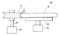
- FIG. 1 It is a top view explaining circular motion which does not involve rotation of a carrier plate in a fixed abrasive processing device used in a simultaneous grinding process of front and back among semiconductor wafer manufacturing methods concerning Example 1 of this invention. It is a front view which shows the use condition of the chamfering apparatus used at the chamfering process of a semiconductor wafer among the manufacturing methods of the semiconductor wafer which concerns on Example 1 of this invention.
- FIG. 1 is a perspective view of a planetary gear type double-side polishing apparatus used in a semiconductor wafer double-side polishing step in a semiconductor wafer manufacturing method according to Embodiment 1 of the present invention; It is a front view which shows the collection
- the semiconductor wafer manufacturing method according to the first embodiment includes a crystal pulling step S101, a crystal processing step S102, a slicing step S103, a fixed abrasive double-sided grinding step S104, a chamfering step S105, and double-side polishing.
- Step S106 and finish polishing step S107 are provided.
- the crystal pulling step S101 from a silicon melt doped with a predetermined amount of boron in the crucible, the diameter is 306 mm, the length of the straight body is 2500 mm, the specific resistance is 0.01 ⁇ ⁇ cm, the initial oxygen is obtained by the Czochralski method. A single crystal silicon ingot having a concentration of 1.0 ⁇ 10 18 atoms / cm 3 is pulled up.
- each crystal block I is formed in a cylindrical shape.
- a wire saw 40 is used to slice a large number of silicon wafers having a diameter of 300 mm from the crystal block I.
- the wire saw 40 includes three wire saw groove rollers (hereinafter referred to as groove rollers) 41A to 41C arranged in a triangular shape when viewed from the front. Between these groove rollers 41A to 41C, one fixed abrasive wire 42 is wound at a constant pitch so as to be parallel to each other. As a result, the wire row 45 appears between the groove rollers 41A to 41C.
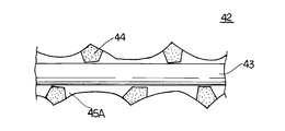
- the fixed abrasive wire 42 is obtained by fixing diamond abrasive grains 44 having a particle diameter of 15 to 25 ⁇ m to a surface of a steel wire 43 having a diameter of 160 ⁇ m by a nickel plating 45A having a thickness of 7 ⁇ m (FIG. 3).
- the fixed abrasive wire 42 is led out from the bobbin of the feeding device, is laid over each of the groove rollers 41A to 41C via the supply-side guide roller, and then is passed through the guide roller on the lead-out side of the winding device. It is wound on a bobbin. Since the fixed abrasive wire 42 reciprocates, the roles of the feeding device and the winding device are alternately changed.
- the wire row 45 is reciprocated by the main motor between the three groove rollers 41A to 41C.
- the middle of the two groove rollers 41A and 41B arranged on the lower side is the cutting position of the crystal block I.
- a pure water supply nozzle 46 for continuously supplying pure water onto the wire row 45 is provided above one side of the cutting position. While supplying 10 liter / min of pure water from the pure water supply nozzle 46 to the wire row 45, the crystal block I is pressed at 1.0 mm / min from below onto the wire row 45 that is reciprocating at 1 m / min.
- reference numeral 47 denotes a lifting block for the crystal block I.
- the fixed abrasive double-side grinding step S104 the front and back surfaces of the silicon wafer are ground simultaneously while supplying pure water using a non-sun gear fixed abrasive processing apparatus.
- the fixed abrasive processing apparatus 10 will be described in detail with reference to FIGS.
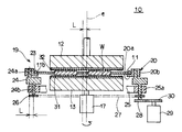
- the fixed abrasive processing apparatus 10 includes a carrier plate 11 made of glass epoxy having a disk shape in plan view in which three wafer holding holes 11a are formed around the plate axis (in the circumferential direction) every 120 °; An upper surface plate that grinds the front and back surfaces of the wafer by sandwiching the silicon wafer W inserted and held in each wafer holding hole 11a so as to be pivotable from above and below and moving it relative to the silicon wafer W (grinding) And a lower surface plate (a lower surface plate for grinding) 13.
- the thickness (700 ⁇ m) of the carrier plate 11 is slightly smaller than the thickness (780 ⁇ m) of the silicon wafer W.
- a lower processing layer (fixed abrasive layer) 31 is formed on the upper surface (surface plate surface) of the lower surface plate 13, and an upper processing layer (another fixed abrasive layer) 32 on the lower surface (surface plate surface) of the upper surface plate 12. Is formed.
- the lower processed layer 31 and the upper processed layer 32 are diamond abrasive grains (fixed abrasive grains) having a particle size (average particle size) of less than 4 ⁇ m (for example, 0.5 ⁇ m or more and less than 4 ⁇ m) over the entire surface of the elastic base materials 31a and 32a.
- 31b and 32b are provided by adhering a grinding stone piece a of several mm square (0.1 mm square to 10 mm square) with an adhesive so that the degree of concentration is 100.
- a cured polymer system for example, epoxy resin, phenol resin, acrylic urethane resin, polyurethane resin, vinyl chloride resin, fluorine resin
- Its thickness is 800 ⁇ m.
- the grindstone pieces a including the diamond abrasive grains 31b and 32b are bonded to the surfaces of the elastic base materials 31a and 32a to form the two processed layers 31 and 32.
- Both processed layers 31 and 32 may be formed by directly bonding the diamond abrasive grains 31b and 32b.
- the upper surface plate 12 is rotationally driven in the horizontal plane by the upper rotation motor 16 via a rotating shaft 12a extending upward. Further, the upper surface plate 12 is vertically moved up and down by an elevating device 18 that advances and retracts in the axial direction.
- the elevating device 18 is used, for example, when the silicon wafer W is supplied to and discharged from the carrier plate 11.
- the surface pressure of 250 g / cm 2 on the upper and lower surfaces of the silicon wafer W of the upper surface plate 12 and the lower surface plate 13 is applied by pressure means such as an air bag system (not shown) incorporated in the upper surface plate 12 and the lower surface plate 13. Done.
- the lower surface plate 13 is rotated in the horizontal plane by the lower rotation motor 17 via the output shaft 17a.
- the carrier plate 11 is circularly moved in a plane (horizontal plane) parallel to the surface of the plate 11 by the carrier circular motion mechanism 19 so that the plate 11 itself does not rotate.
- the carrier circular motion mechanism 19 has an annular carrier holder 20 that holds the carrier plate 11 from the outside.
- the carrier circular motion mechanism 19 and the carrier holder 20 are connected via a connection structure.
- the connection structure is means for connecting the carrier plate 11 to the carrier holder 20 so that the carrier plate 11 does not rotate and can absorb the elongation of the carrier plate 11 during thermal expansion. That is, as shown in FIG. 4 and FIG. 5, the connecting structure includes a large number of pins 23 projecting from the inner peripheral flange 20 a of the carrier holder 20 at predetermined angles in the holder circumferential direction, and the outer periphery of the carrier plate 11. Among the portions, each pin 23 has a long hole-shaped pin hole 11b formed in a number corresponding to the corresponding position.
- Each pin hole 11b has its hole length direction aligned with the plate radial direction so that the carrier plate 11 connected to the carrier holder 20 via the pin 23 can move slightly in the radial direction.
- the outer periphery of the carrier holder 20 is provided with four bearing portions 20b that protrude outward every 90 °.
- Each bearing portion 20b is provided with an eccentric shaft 24a projecting at an eccentric position on the upper surface of the small-diameter disk-shaped eccentric arm 24.
- a rotating shaft 24 b is suspended from the center of each lower surface of the four eccentric arms 24.
- Each rotary shaft 24b is attached to a bearing portion 25a disposed on the annular device base 25 every 90 ° in a state where each tip portion protrudes downward.
- a sprocket 26 is fixed to the tip of each rotating shaft 24b protruding downward.
- Each sprocket 26 has a series of timing chains 27 in a horizontal state.
- Each sprocket 26 and the timing chain 27 constitute synchronizing means for simultaneously rotating the four rotating shafts 24b so that the four eccentric arms 24 perform a circular motion in synchronization.
- one rotating shaft 24b is formed to be longer, and a tip portion thereof projects downward from the sprocket 26.
- a power transmission gear 28 is fixed to this portion.
- the gear 28 is engaged with a large-diameter driving gear 30 fixed to an output shaft extending upward of a circular motion motor 29 such as a geared motor.
- a circular motion motor 29 for circular motion may be arrange
- the carrier holder 20 collectively connected to each eccentric shaft 24 a, and by extension, the carrier plate 11 held by the holder 20, performs a circular motion without rotation in a horizontal plane parallel to the plate 11.
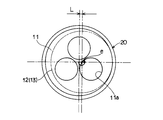
- the center line of the carrier plate 11 turns while maintaining a state of being eccentric from the axis e of both surface plates 12 and 13 by a distance L.
- This distance L is the same as the distance between the eccentric shaft 24a and the rotating shaft 24b. Due to this circular motion without rotation, all points on the carrier plate 11 draw a locus of a small circle of the same size (FIG. 6).
- the silicon wafer W is inserted into each wafer holding hole 11a of the carrier plate 11 so as to be rotatable.
- the upper processing layer 32 rotating at 15 rpm together with the upper surface plate 12 is pressed against each wafer W at 250 g / cm 2
- the lower processing layer 31 rotating at 15 rpm together with the lower surface plate 13 is pressed.
- the timing chain 27 is rotated by the circular motion motor 29 while supplying pure water from the upper surface plate 12 at 2 liters / minute while pressing both the processed layers 31 and 32 against the front and back surfaces of the wafer.
- each eccentric arm 24 rotates synchronously in a horizontal plane, and the carrier holder 20 and the carrier plate 11 collectively connected to each eccentric shaft 24a are rotated in a horizontal plane parallel to the surface of the plate 11.
- the front and back surfaces of the three silicon wafers W are simultaneously ground while each silicon wafer W rotates in a horizontal plane in the corresponding wafer holding hole 11a.
- the grinding amount is 30 ⁇ m on one side of the wafer and 60 ⁇ m on the wafer front and back sides (processing strain is 15 ⁇ m on one side, 30 ⁇ m on both sides).
- the silicon wafer W is processed three by three by the fixed abrasive type fixed abrasive processing apparatus 10 that can perform rough grinding to finish grinding in one step, the number of manufacturing steps of the silicon wafer W can be reduced. Moreover, since the crystal block I is sliced by the fixed abrasive wire 42 during the above-described slicing as well as the double-sided simultaneous grinding of the fixed abrasive method, kerf loss during wafer manufacture can be reduced. Also, using the non-sun gear type fixed abrasive machining apparatus 10, the surface pressure is increased to 250 g / cm 2, which is higher than that of the sun gear method (100 to 150 g / cm 2 ), and circular motion without rotation is performed. However, since the front and back surfaces of each silicon wafer W are ground simultaneously, it is possible to realize high-precision processing with few scratches on the ground surface (processed surface) while having a high processing rate of 15 ⁇ m / min.
- the silicon wafer W is processed using the diamond abrasive grains 31b and 32b of less than 4 ⁇ m adhered on the surfaces of the elastic base materials 31a and 32a using the fixed abrasive processing apparatus 10, the silicon after slicing A surface having good flatness can be obtained for the wafer W.
- the silicon wafer W is in a free state placed in the wafer holding hole 11a of the carrier plate 11, in addition to good flatness, a good nanotopography (appears on the surface when the silicon wafer W is not attracted). Swell) can be obtained.
- the elastic base materials 31a and 32a have elasticity, when the diamond abrasive grains 31b and 32b are pressed against the silicon wafer W, the elastic base material 31a and 32b receive the force that the silicon wafer W receives from the diamond abrasive grains 31b and 32b. 32a is mitigated, and it is possible to prevent the silicon wafer W from being damaged by local and excessive external force acting on the silicon wafer W.
- the use of fine diamond abrasive grains 31b and 32b of less than 4 ⁇ m employs a method in which the fixed abrasive processing apparatus 10 fixes the diamond abrasive grains 31b and 32b to the upper surface plate 12 and the lower surface plate 13 to perform wafer processing. This is possible. That is, for example, in the conventional lapping apparatus, since the free abrasive grains are employed as the abrasive grains, it is difficult to reduce the grain size.
- the chamfering grindstone 51 during rotation of the chamfering device 50 is pressed against the outer peripheral portion of the silicon wafer W to chamfer (FIG. 7).
- the chamfering device 50 used here is a device that chamfers the outer peripheral portion of the silicon wafer W by pressing the outer peripheral portion of the silicon wafer W against the grinding surface (outer peripheral surface) of the rotating # 800 chamfering grindstone 51. is there.
- the silicon wafer W is vacuum-sucked on the upper surface of the turntable 52, and the turntable 52 is rotatably provided by a table motor 53. Further, a chamfering grindstone 51 is disposed in proximity to the rotary table 52.
- the chamfering grindstone 51 is fixed to the tip of the rotation shaft 55 of the rotary motor 54 and is supported so as to be rotatable about the rotation shaft 55.
- pure water is supplied to the chamfered surface of the silicon wafer W at 5 liters / minute.
- the chamfered surface of the silicon wafer W may be mirrored after the chamfering step S105. Specifically, the chamfered portion (chamfered surface) of the silicon wafer W is pressed against a rotating cloth or buff around a vertical rotation axis, and the chamfered surface of the chamfered portion is finished to be a mirror surface.
- a planetary gear type double-side polishing apparatus is used to polish the front and back surfaces (both sides) of a large number of silicon wafers W using a polishing liquid containing loose abrasive grains.
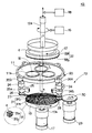
- the planetary gear type double-side polishing apparatus 60 will be described in detail with reference to FIG.
- the double-side polishing apparatus 60 includes an upper surface plate 61 and a lower surface plate 62 that are arranged in parallel, a small-diameter sun gear 63 that is interposed between both surface plates 61 and 62 and that is rotatable about an axis, A large-diameter internal gear 64 provided rotatably around the same axis as this axis, and a total of four small-diameter disk-shaped carrier plates 65 are provided.
- An upper polishing cloth 66 is stretched on the lower surface of the upper surface plate 61, and a lower polishing cloth 67 is stretched on the upper surface of the lower surface plate 62.
- Each carrier plate 65 is formed with four wafer holding holes 65a.
- an outer gear 65 b that meshes with the sun gear 63 and the internal gear 64 is formed at the outer edge of the carrier plate 65.
- a method for simultaneously polishing the front and back surfaces of the silicon wafer W by the double-side polishing apparatus 60 will be described.
- Each carrier plate 65 is rotated and revolved between the upper surface plate 61 and the lower surface plate 62 while supplying the polishing liquid, and the surface of the four silicon wafers W held in the wafer holding holes 65a of each carrier plate 65 is displayed.
- the back surface is mechanically and chemically polished while being pressed against the corresponding upper polishing cloth 66 and lower polishing cloth 67.
- colloidal silica in which baked silica is dispersed in an aqueous solution is employed.
- the sun gear 63 and the internal gear 64 are rotated in directions opposite to each other. Thereby, the front and back surfaces of the silicon wafers W are simultaneously polished by 20 ⁇ m.
- a single-side polishing apparatus (not shown) is used to finish and polish the surface of a large number of silicon wafers W into a mirror surface.
- the single-side polishing apparatus includes a polishing surface plate on which a polishing cloth made of a hard urethane pad is stretched on the upper surface, and a polishing head disposed above the polishing surface plate. On the lower surface of the polishing head, three silicon wafers W, the surface of which is disposed downward, are attached by wax via a carrier plate.
- the polishing head is gradually lowered while rotating the polishing surface plate and the polishing head at a predetermined direction and at a predetermined speed, and pressed against the polishing cloth supplied with the polishing liquid at 5 liters / minute. Thereby, the surface of each silicon wafer W is mirror-polished by 0.5 ⁇ m.
- the chamfering using the chamfering device 50 is performed.
- the used processing fluid waste water
- pure water can be adopted as a working fluid used in these three steps.
- silicon scrap semiconductor scrap
- silicon scrap recovery equipment 70 shown in FIG. 9 silicon scrap (semiconductor scrap) is recovered from a used slurry containing a conventional oil-based dispersant and free abrasive grains and reused. Compared to the above, the reuse process can be facilitated, and the processing cost can be reduced.
- the recovery facility 70 stores a first sub tank 71 that stores waste water from the wire saw 40, a second sub tank 72 that stores waste water from the fixed abrasive grain processing device 10, and a first sub tank that stores waste water from the chamfering device 50. 3 sub-tanks 73.
- Each of the sub tanks 71 to 73 is provided with a stirrer 74 that stirs the stored waste water.
- An upstream end portion of a branch pipe 76a provided with an on-off valve 75 is connected to the bottom plate of each of the sub tanks 71 to 73.
- the downstream end of each branch pipe 76a is the upstream end of the introduction pipe 76 in which the downstream end communicates with the inside of the bottom of the recovery tank (water tank) 77, the intermediate portion in the length direction. , Communicated with the downstream part.
- the waste water in each of the sub tanks 71 to 73 is introduced into the recovery tank 77 through each branch pipe 76a and the introduction pipe 76.
- the three types of waste water are dispersed and mixed by the stirrer 74 and then led out through the lead-out pipe 78.
- the silicon waste S is centrifuged from the mixed waste liquid by the cyclone separator 79 provided in the intermediate portion of the outlet pipe 78.
- the separated silicon waste S falls directly below and is collected in the waste receiving tank 80.
- the recovered silicon scrap S is subjected to post-processing called metal removal cleaning.
- the post-processed silicon scrap S is put into a crucible of a Czochralski-type single crystal silicon pulling apparatus and reused as a raw material for the single crystal silicon ingot.
- the present invention is useful for reducing industrial waste (semiconductor waste) discharged from a semiconductor manufacturing factory and reusing this industrial waste.
Landscapes
- Engineering & Computer Science (AREA)
- Mechanical Engineering (AREA)
- Chemical & Material Sciences (AREA)
- Ceramic Engineering (AREA)
- Inorganic Chemistry (AREA)
- Mechanical Treatment Of Semiconductor (AREA)
- Grinding Of Cylindrical And Plane Surfaces (AREA)
- Grinding-Machine Dressing And Accessory Apparatuses (AREA)
- Processing Of Stones Or Stones Resemblance Materials (AREA)
Abstract
Priority Applications (3)
| Application Number | Priority Date | Filing Date | Title |
|---|---|---|---|
| US13/581,011 US20120315739A1 (en) | 2010-02-26 | 2011-02-16 | Manufacturing method for semiconductor wafer |
| JP2012501747A JPWO2011105255A1 (ja) | 2010-02-26 | 2011-02-16 | 半導体ウェーハの製造方法 |
| DE112011100688T DE112011100688T5 (de) | 2010-02-26 | 2011-02-16 | Verfahren zum Herstellen eines Halbleiterwafers |
Applications Claiming Priority (2)
| Application Number | Priority Date | Filing Date | Title |
|---|---|---|---|
| JP2010-043150 | 2010-02-26 | ||
| JP2010043150 | 2010-02-26 |
Publications (1)
| Publication Number | Publication Date |
|---|---|
| WO2011105255A1 true WO2011105255A1 (fr) | 2011-09-01 |
Family
ID=44506669
Family Applications (1)
| Application Number | Title | Priority Date | Filing Date |
|---|---|---|---|
| PCT/JP2011/053193 Ceased WO2011105255A1 (fr) | 2010-02-26 | 2011-02-16 | Procédé de fabrication de tranche de semi-conducteur |
Country Status (5)
| Country | Link |
|---|---|
| US (1) | US20120315739A1 (fr) |
| JP (1) | JPWO2011105255A1 (fr) |
| KR (1) | KR20120091371A (fr) |
| DE (1) | DE112011100688T5 (fr) |
| WO (1) | WO2011105255A1 (fr) |
Cited By (6)
| Publication number | Priority date | Publication date | Assignee | Title |
|---|---|---|---|---|
| WO2014129304A1 (fr) * | 2013-02-19 | 2014-08-28 | 株式会社Sumco | Procédé de traitement de tranche de semi-conducteur |
| JP2015008247A (ja) * | 2013-06-26 | 2015-01-15 | 株式会社Sumco | 半導体ウェーハの加工プロセス |
| WO2015097989A1 (fr) * | 2013-12-26 | 2015-07-02 | 信越半導体株式会社 | Procédé de tranchage |
| CN106181747B (zh) * | 2016-06-13 | 2018-09-04 | 江苏吉星新材料有限公司 | 一种大尺寸蓝宝石超薄双面抛光窗口片加工方法 |
| JP2020031181A (ja) * | 2018-08-24 | 2020-02-27 | 株式会社荏原製作所 | 基板処理装置、基板処理方法、及び基板処理装置を制御する方法をコンピュータに実行させるためのプログラムを格納した記憶媒体 |
| JP7072180B1 (ja) | 2021-12-20 | 2022-05-20 | 有限会社サクセス | 半導体結晶ウェハの製造方法および製造装置 |
Families Citing this family (14)
| Publication number | Priority date | Publication date | Assignee | Title |
|---|---|---|---|---|
| KR101271444B1 (ko) * | 2009-06-04 | 2013-06-05 | 가부시키가이샤 사무코 | 고정 연마 입자 가공 장치 및 고정 연마 입자 가공 방법, 그리고 반도체 웨이퍼 제조 방법 |
| CN105451938A (zh) * | 2013-08-09 | 2016-03-30 | 福吉米株式会社 | 研磨加工工具以及构件的加工方法 |
| KR101895817B1 (ko) * | 2014-06-02 | 2018-09-07 | 가부시키가이샤 사무코 | 실리콘 웨이퍼 및 그 제조 방법 |
| US10000863B2 (en) * | 2015-02-03 | 2018-06-19 | Sumco Corporation | Method for cleaning single crystal pulling apparatus, cleaning tool for use therein, and method for manufacturing single crystal |
| MY186276A (en) | 2015-05-13 | 2021-07-02 | Shinetsu Chemical Co | Method for producing substrates |
| KR101971150B1 (ko) * | 2017-08-18 | 2019-04-22 | 에스케이실트론 주식회사 | 웨이퍼의 에지 연마부, 이를 포함하는 웨이퍼의 에지 연마 장치 및 방법 |
| JP7075808B2 (ja) * | 2018-04-20 | 2022-05-26 | 株式会社ディスコ | 切削装置 |
| US11309188B2 (en) * | 2018-05-09 | 2022-04-19 | Semiconductor Components Industries, Llc | Singulation of silicon carbide semiconductor wafers |
| JP7242220B2 (ja) * | 2018-09-03 | 2023-03-20 | キヤノン株式会社 | 接合ウェハ及びその製造方法、並びにスルーホール形成方法 |
| US11621171B2 (en) * | 2018-09-25 | 2023-04-04 | Nissan Chemical Corporation | Method for polishing silicon wafer with reduced wear on carrier, and polishing liquid used therein |
| WO2021092376A1 (fr) | 2019-11-08 | 2021-05-14 | Mosaic Microsystems Llc | Plaquette inorganique traitée et traitement d'un empilement de plaquettes avec un procédé abrasif |
| EP4055426B1 (fr) | 2019-11-08 | 2025-04-09 | Mosaic Microsystems LLC | Facilitation de la formation d'un trou d'interconnexion dans un substrat |
| CN118977161B (zh) * | 2024-10-22 | 2025-01-03 | 北京特思迪半导体设备有限公司 | 一种压头以及具有该压头的晶圆打磨装置 |
| CN121589709A (zh) * | 2025-10-20 | 2026-03-03 | 苏州光斯奥光电科技有限公司 | 屏显玻璃单边研磨工艺 |
Citations (4)
| Publication number | Priority date | Publication date | Assignee | Title |
|---|---|---|---|---|
| JP2002050596A (ja) * | 2000-08-02 | 2002-02-15 | Sanyo Electric Co Ltd | 半導体結晶物の処理システムおよび半導体ウェハの処理システム |
| JP2004319951A (ja) * | 2003-04-02 | 2004-11-11 | Sumitomo Electric Ind Ltd | エッジ研磨した窒化物半導体基板とエッジ研磨したGaN自立基板及び窒化物半導体基板のエッジ加工方法 |
| JP2007301687A (ja) * | 2006-05-12 | 2007-11-22 | Naoetsu Electronics Co Ltd | ワーク切断装置 |
| JP2009302409A (ja) * | 2008-06-16 | 2009-12-24 | Sumco Corp | 半導体ウェーハの製造方法 |
Family Cites Families (24)
| Publication number | Priority date | Publication date | Assignee | Title |
|---|---|---|---|---|
| JPH08197400A (ja) * | 1995-01-25 | 1996-08-06 | Sumitomo Sitix Corp | 半導体ウェーハの面取り部研磨方法 |
| JPH11154655A (ja) * | 1997-11-21 | 1999-06-08 | Komatsu Electron Metals Co Ltd | 半導体ウェハの製造方法 |
| JP2000114216A (ja) * | 1998-10-01 | 2000-04-21 | Sumitomo Metal Ind Ltd | 半導体ウェーハの製造方法 |
| US6746309B2 (en) * | 1999-05-27 | 2004-06-08 | Sanyo Electric Co., Ltd. | Method of fabricating a semiconductor device |
| EP1313135A1 (fr) * | 2000-06-29 | 2003-05-21 | Shin-Etsu Handotai Co., Ltd | Procede de traitement d'une plaquette de semi-conducteur et plaquette de semi-conducteur |
| JP2002124490A (ja) * | 2000-08-03 | 2002-04-26 | Sumitomo Metal Ind Ltd | 半導体ウェーハの製造方法 |
| DE10157433B4 (de) * | 2000-11-24 | 2019-05-29 | Hitachi Metals, Ltd. | Verfahren zum Schneiden einer Seltenerdmetall-Legierung, Verfahren zur Herstellung eines Seltenerdmetall-Magneten und Drahtsäge-Vorrichtung |
| JP2003022989A (ja) * | 2001-07-09 | 2003-01-24 | Sumitomo Mitsubishi Silicon Corp | エピタキシャル半導体ウェーハ及びその製造方法 |
| JP4192482B2 (ja) * | 2002-03-22 | 2008-12-10 | 株式会社Sumco | シリコンウェーハの製造方法 |
| JP2004050384A (ja) * | 2002-07-24 | 2004-02-19 | Hitachi Zosen Corp | 研磨装置 |
| US7416962B2 (en) * | 2002-08-30 | 2008-08-26 | Siltronic Corporation | Method for processing a semiconductor wafer including back side grinding |
| JP4248895B2 (ja) * | 2003-02-27 | 2009-04-02 | Sumco Techxiv株式会社 | スラリ再生方法及びワイヤソーシステム |
| KR100797734B1 (ko) * | 2003-12-05 | 2008-01-24 | 가부시키가이샤 섬코 | 편면 경면 웨이퍼의 제조 방법 |
| JP4424039B2 (ja) * | 2004-04-02 | 2010-03-03 | 株式会社Sumco | 半導体ウェーハの製造方法 |
| JP2006073747A (ja) * | 2004-09-01 | 2006-03-16 | Sumco Corp | 半導体ウェーハの処理方法およびその装置 |
| JP4517867B2 (ja) * | 2005-01-31 | 2010-08-04 | 株式会社Sumco | シリコンウェーハ表面形状制御用エッチング液及び該エッチング液を用いたシリコンウェーハの製造方法 |
| JP4835069B2 (ja) * | 2005-08-17 | 2011-12-14 | 株式会社Sumco | シリコンウェーハの製造方法 |
| KR101460993B1 (ko) * | 2007-01-31 | 2014-11-13 | 신에쯔 한도타이 가부시키가이샤 | 실리콘 웨이퍼의 면취 장치 및 실리콘 웨이퍼의 제조방법 그리고 에치드 실리콘 웨이퍼 |
| JP5557391B2 (ja) * | 2007-10-30 | 2014-07-23 | ポール・コーポレーション | 基板材料からウェハ状スライスを製造するための方法及びシステム |
| JP5600867B2 (ja) * | 2008-06-16 | 2014-10-08 | 株式会社Sumco | 半導体ウェーハの製造方法 |
| JP2009302410A (ja) * | 2008-06-16 | 2009-12-24 | Sumco Corp | 半導体ウェーハの製造方法 |
| JP2010017811A (ja) * | 2008-07-11 | 2010-01-28 | Sumco Corp | 半導体ウェーハの製造方法 |
| JP2010029998A (ja) * | 2008-07-30 | 2010-02-12 | Japan Fine Steel Co Ltd | 固定砥粒ワイヤソーに使用したクーラントの処理方法及びその処理装置 |
| KR20110104066A (ko) * | 2008-12-20 | 2011-09-21 | 캐보트 마이크로일렉트로닉스 코포레이션 | 와이어 쏘잉 동안 건조 상태를 개선시키는 조성물 |
-
2011
- 2011-02-16 WO PCT/JP2011/053193 patent/WO2011105255A1/fr not_active Ceased
- 2011-02-16 US US13/581,011 patent/US20120315739A1/en not_active Abandoned
- 2011-02-16 JP JP2012501747A patent/JPWO2011105255A1/ja active Pending
- 2011-02-16 DE DE112011100688T patent/DE112011100688T5/de not_active Ceased
- 2011-02-16 KR KR1020127015531A patent/KR20120091371A/ko not_active Ceased
Patent Citations (4)
| Publication number | Priority date | Publication date | Assignee | Title |
|---|---|---|---|---|
| JP2002050596A (ja) * | 2000-08-02 | 2002-02-15 | Sanyo Electric Co Ltd | 半導体結晶物の処理システムおよび半導体ウェハの処理システム |
| JP2004319951A (ja) * | 2003-04-02 | 2004-11-11 | Sumitomo Electric Ind Ltd | エッジ研磨した窒化物半導体基板とエッジ研磨したGaN自立基板及び窒化物半導体基板のエッジ加工方法 |
| JP2007301687A (ja) * | 2006-05-12 | 2007-11-22 | Naoetsu Electronics Co Ltd | ワーク切断装置 |
| JP2009302409A (ja) * | 2008-06-16 | 2009-12-24 | Sumco Corp | 半導体ウェーハの製造方法 |
Cited By (10)
| Publication number | Priority date | Publication date | Assignee | Title |
|---|---|---|---|---|
| WO2014129304A1 (fr) * | 2013-02-19 | 2014-08-28 | 株式会社Sumco | Procédé de traitement de tranche de semi-conducteur |
| JPWO2014129304A1 (ja) * | 2013-02-19 | 2017-02-02 | 株式会社Sumco | 半導体ウェーハの加工方法 |
| US9881783B2 (en) | 2013-02-19 | 2018-01-30 | Sumco Corporation | Method for processing semiconductor wafer |
| JP2015008247A (ja) * | 2013-06-26 | 2015-01-15 | 株式会社Sumco | 半導体ウェーハの加工プロセス |
| WO2015097989A1 (fr) * | 2013-12-26 | 2015-07-02 | 信越半導体株式会社 | Procédé de tranchage |
| JP2015126069A (ja) * | 2013-12-26 | 2015-07-06 | 信越半導体株式会社 | スライス方法 |
| CN106181747B (zh) * | 2016-06-13 | 2018-09-04 | 江苏吉星新材料有限公司 | 一种大尺寸蓝宝石超薄双面抛光窗口片加工方法 |
| JP2020031181A (ja) * | 2018-08-24 | 2020-02-27 | 株式会社荏原製作所 | 基板処理装置、基板処理方法、及び基板処理装置を制御する方法をコンピュータに実行させるためのプログラムを格納した記憶媒体 |
| JP7072180B1 (ja) | 2021-12-20 | 2022-05-20 | 有限会社サクセス | 半導体結晶ウェハの製造方法および製造装置 |
| JP2023091696A (ja) * | 2021-12-20 | 2023-06-30 | 有限会社サクセス | 半導体結晶ウェハの製造方法および製造装置 |
Also Published As
| Publication number | Publication date |
|---|---|
| DE112011100688T5 (de) | 2013-02-28 |
| US20120315739A1 (en) | 2012-12-13 |
| JPWO2011105255A1 (ja) | 2013-06-20 |
| KR20120091371A (ko) | 2012-08-17 |
Similar Documents
| Publication | Publication Date | Title |
|---|---|---|
| WO2011105255A1 (fr) | Procédé de fabrication de tranche de semi-conducteur | |
| CN102069448B (zh) | 半导体晶片的制造方法 | |
| JP3400765B2 (ja) | 半導体ウェハの製造方法および該製造方法の使用 | |
| JP5913839B2 (ja) | 研磨方法 | |
| Li et al. | Machining processes for sapphire wafers: a literature review | |
| CN102484042B (zh) | 生产半导体晶片的方法 | |
| US9550264B2 (en) | Fixed abrasive-grain processing device, method of fixed abrasive-grain processing, and method for producing semiconductor wafer | |
| US20150162181A1 (en) | Semiconductor wafer manufacturing method | |
| JP6079554B2 (ja) | 半導体ウェーハの製造方法 | |
| JP2011155265A (ja) | 半導体ウェハの製造方法 | |
| JP6747599B2 (ja) | シリコンウェーハの両面研磨方法 | |
| CN115319564B (zh) | 基于恒压复合固结磨粒的硬脆性晶圆材料减薄装置和方法 | |
| KR20120042674A (ko) | 경취성 웨이퍼의 평탄화 가공 방법 및 평탄화 가공용 패드 | |
| EP1759810B1 (fr) | Méthode de polissage de plaquette | |
| JP2013045909A (ja) | 半導体ウェーハの製造方法 | |
| WO2004107428A1 (fr) | Procede de production pour plaquettes de semi-conducteur | |
| KR101303552B1 (ko) | 반도체 웨이퍼의 양면을 화학적으로 그라인딩하는 방법 | |
| JP2010131683A (ja) | シリコンウェーハの研磨方法 | |
| JP2004356336A (ja) | 半導体ウェーハの両面研磨方法 | |
| EP2192609A1 (fr) | Procédé de fabrication d'une tranche pour une couche active | |
| JPH1058306A (ja) | 研磨布のドレッシング装置および研磨布ドレッシング用砥石 | |
| JP2001007064A (ja) | 半導体ウエーハの研削方法 | |
| CN112548883A (zh) | 研磨砂轮及研磨设备 | |
| KR100584043B1 (ko) | 화학적 기계적 연마장치를 위한 컨디셔닝 장치 | |
| JP2004238566A (ja) | 研磨用スラリの製造方法 |
Legal Events
| Date | Code | Title | Description |
|---|---|---|---|
| 121 | Ep: the epo has been informed by wipo that ep was designated in this application |
Ref document number: 11747219 Country of ref document: EP Kind code of ref document: A1 |
|
| WWE | Wipo information: entry into national phase |
Ref document number: 2012501747 Country of ref document: JP |
|
| ENP | Entry into the national phase |
Ref document number: 20127015531 Country of ref document: KR Kind code of ref document: A |
|
| WWE | Wipo information: entry into national phase |
Ref document number: 13581011 Country of ref document: US |
|
| WWE | Wipo information: entry into national phase |
Ref document number: 1120111006888 Country of ref document: DE Ref document number: 112011100688 Country of ref document: DE |
|
| 122 | Ep: pct application non-entry in european phase |
Ref document number: 11747219 Country of ref document: EP Kind code of ref document: A1 |