EP4060355A1 - Schutz des inhalts eines schmelzspeichers - Google Patents
Schutz des inhalts eines schmelzspeichers Download PDFInfo
- Publication number
- EP4060355A1 EP4060355A1 EP22162199.8A EP22162199A EP4060355A1 EP 4060355 A1 EP4060355 A1 EP 4060355A1 EP 22162199 A EP22162199 A EP 22162199A EP 4060355 A1 EP4060355 A1 EP 4060355A1
- Authority
- EP
- European Patent Office
- Prior art keywords
- state
- circuit
- word
- fuse
- memory
- Prior art date
- Legal status (The legal status is an assumption and is not a legal conclusion. Google has not performed a legal analysis and makes no representation as to the accuracy of the status listed.)
- Granted
Links
Images


Classifications
-
- G—PHYSICS
- G01—MEASURING; TESTING
- G01R—MEASURING ELECTRIC VARIABLES; MEASURING MAGNETIC VARIABLES
- G01R31/00—Arrangements for testing electric properties; Arrangements for locating electric faults; Arrangements for electrical testing characterised by what is being tested not provided for elsewhere
- G01R31/28—Testing of electronic circuits, e.g. by signal tracer
- G01R31/317—Testing of digital circuits
- G01R31/31719—Security aspects, e.g. preventing unauthorised access during test
-
- G—PHYSICS
- G11—INFORMATION STORAGE
- G11C—STATIC STORES
- G11C29/00—Checking stores for correct operation ; Subsequent repair; Testing stores during standby or offline operation
- G11C29/52—Protection of memory contents; Detection of errors in memory contents
-
- G—PHYSICS
- G01—MEASURING; TESTING
- G01R—MEASURING ELECTRIC VARIABLES; MEASURING MAGNETIC VARIABLES
- G01R31/00—Arrangements for testing electric properties; Arrangements for locating electric faults; Arrangements for electrical testing characterised by what is being tested not provided for elsewhere
- G01R31/28—Testing of electronic circuits, e.g. by signal tracer
- G01R31/317—Testing of digital circuits
- G01R31/3181—Functional testing
- G01R31/3185—Reconfiguring for testing, e.g. LSSD, partitioning
- G01R31/318533—Reconfiguring for testing, e.g. LSSD, partitioning using scanning techniques, e.g. LSSD, Boundary Scan, JTAG
- G01R31/318583—Design for test
- G01R31/318588—Security aspects
-
- G—PHYSICS
- G06—COMPUTING OR CALCULATING; COUNTING
- G06F—ELECTRIC DIGITAL DATA PROCESSING
- G06F1/00—Details not covered by groups G06F3/00 - G06F13/00 and G06F21/00
- G06F1/24—Resetting means
-
- G—PHYSICS
- G06—COMPUTING OR CALCULATING; COUNTING
- G06F—ELECTRIC DIGITAL DATA PROCESSING
- G06F12/00—Accessing, addressing or allocating within memory systems or architectures
- G06F12/14—Protection against unauthorised use of memory or access to memory
- G06F12/1458—Protection against unauthorised use of memory or access to memory by checking the subject access rights
-
- G—PHYSICS
- G06—COMPUTING OR CALCULATING; COUNTING
- G06F—ELECTRIC DIGITAL DATA PROCESSING
- G06F9/00—Arrangements for program control, e.g. control units
- G06F9/06—Arrangements for program control, e.g. control units using stored programs, i.e. using an internal store of processing equipment to receive or retain programs
- G06F9/44—Arrangements for executing specific programs
- G06F9/448—Execution paradigms, e.g. implementations of programming paradigms
- G06F9/4498—Finite state machines
-
- G—PHYSICS
- G11—INFORMATION STORAGE
- G11C—STATIC STORES
- G11C29/00—Checking stores for correct operation ; Subsequent repair; Testing stores during standby or offline operation
- G11C29/02—Detection or location of defective auxiliary circuits, e.g. defective refresh counters
- G11C29/027—Detection or location of defective auxiliary circuits, e.g. defective refresh counters in fuses
-
- G—PHYSICS
- G11—INFORMATION STORAGE
- G11C—STATIC STORES
- G11C29/00—Checking stores for correct operation ; Subsequent repair; Testing stores during standby or offline operation
- G11C29/04—Detection or location of defective memory elements, e.g. cell constructio details, timing of test signals
- G11C29/08—Functional testing, e.g. testing during refresh, power-on self testing [POST] or distributed testing
- G11C29/10—Test algorithms, e.g. memory scan [MScan] algorithms; Test patterns, e.g. checkerboard patterns
-
- G—PHYSICS
- G11—INFORMATION STORAGE
- G11C—STATIC STORES
- G11C29/00—Checking stores for correct operation ; Subsequent repair; Testing stores during standby or offline operation
- G11C29/04—Detection or location of defective memory elements, e.g. cell constructio details, timing of test signals
- G11C29/50—Marginal testing, e.g. race, voltage or current testing
-
- G—PHYSICS
- G11—INFORMATION STORAGE
- G11C—STATIC STORES
- G11C29/00—Checking stores for correct operation ; Subsequent repair; Testing stores during standby or offline operation
- G11C29/54—Arrangements for designing test circuits, e.g. design for test [DFT] tools
-
- G—PHYSICS
- G01—MEASURING; TESTING
- G01R—MEASURING ELECTRIC VARIABLES; MEASURING MAGNETIC VARIABLES
- G01R31/00—Arrangements for testing electric properties; Arrangements for locating electric faults; Arrangements for electrical testing characterised by what is being tested not provided for elsewhere
- G01R31/28—Testing of electronic circuits, e.g. by signal tracer
- G01R31/317—Testing of digital circuits
- G01R31/3181—Functional testing
- G01R31/3185—Reconfiguring for testing, e.g. LSSD, partitioning
- G01R31/318533—Reconfiguring for testing, e.g. LSSD, partitioning using scanning techniques, e.g. LSSD, Boundary Scan, JTAG
- G01R31/318597—JTAG or boundary scan test of memory devices
-
- G—PHYSICS
- G11—INFORMATION STORAGE
- G11C—STATIC STORES
- G11C29/00—Checking stores for correct operation ; Subsequent repair; Testing stores during standby or offline operation
- G11C29/04—Detection or location of defective memory elements, e.g. cell constructio details, timing of test signals
- G11C29/08—Functional testing, e.g. testing during refresh, power-on self testing [POST] or distributed testing
- G11C29/12—Built-in arrangements for testing, e.g. built-in self testing [BIST] or interconnection details
- G11C2029/1206—Location of test circuitry on chip or wafer
Definitions
- the present description relates generally to electronic circuits, and more particularly to integrated circuits comprising a non-volatile memory of the fuse type.
- the present description concerns, in particular, the implementation of a method making it possible to carry out a test of such a circuit.
- Integrated circuits are used in the design of electronic devices with various applications.
- JTAG Joint Test Action Group
- the JTAG interface is commonly used to test memories, in particular non-volatile memories, and is likely to be used in production as well as in the life of the product, in particular during maintenance operations in order to identify potential defects. from manufacturing.
- the integrated circuit is then generally returned to the manufacturer.
- users may wish to return the product to the manufacturer to be re-tested for manufacturing defects. The user does not perform these tests as a routine maintenance operation. The user sees a problem, suspects it might be a manufacturing defect, and returns the product so the manufacturer can run a test scan again to analyze the defect.
- test procedures and the access to the information contained in the memories of an integrated circuit are likely to pose problems in applications where these memories contain information supposed to be hidden from the manufacturer.
- These may be authentication or encryption keys (more generally passwords, codes or keys used in the life of the circuit), software codes or proprietary protocols stored in the circuit during a customization phase carried out by the end user of the circuit or by an intermediary entity between the manufacturer and this user.
- These elements constitute information to be hidden from the manufacturer (secrets), which it is generally not desirable to communicate to the manufacturer of the integrated circuit.
- non-volatile memories of the circuit are of the erasable or reprogrammable type (flash memory or EPROM), it is possible to erase areas of the memory containing the "secret" before returning the circuit for fault analysis.
- flash memory erasable or reprogrammable type
- EPROM erasable or reprogrammable type
- the non-volatile memories are of the fuse type, their programming is irreversible and it is then problematic to allow access to the circuit via its JTAG interface during the execution of operating tests of the components of the circuit.
- One embodiment overcomes all or part of the drawbacks of known integrated circuit devices.
- An embodiment provides a method in which a state of an integrated circuit enters a first state, authorizing access for reading a first zone of a memory not volatile type fuse to a processing unit, and a second state, prohibiting access for reading of said memory to the processing unit, is conditioned by a verification, by a finite state machine, of a first word of fuse type of said memory, representing a number of transitions to said first state, and a second word of fuse type of said memory, representing a number of transitions to said second state.
- An embodiment provides an integrated circuit comprising a finite state machine conditioning a state of the integrated circuit between a first state, authorizing access for reading a first zone of a non-volatile memory of the fuse type to a processing unit , and a second state, prohibiting access for reading of said memory to the processing unit, to a verification of the values of a first fuse-type word of said memory, representing a number of transitions to said first state, and a second fuse-type word from said memory, representing a number of transitions to said second state.
- said verification consists in comparing the respective values of said first and second words and in verifying the value of the most significant bit of the first word.
- the circuit is in the first state if the value of the second word is lower than the value of the first word or if the most significant bit of the first word is burned out.
- said verification is performed each time the integrated circuit is reset.
- a scan test of the integrated circuit is prohibited.
- a scan test of the integrated circuit is permitted, except for the fuse-type non-volatile memory.
- an incrementation of the second counter is caused exclusively by the state machine.
- an incrementation of the first counter is accessible to the processing unit.
- a transition of said circuit from the first state to the second state is performed if, and only if, on leaving reset, a value entered in a register from outside the circuit while said circuit is being reset, corresponds to a code stored in said first zone of the fuse-type non-volatile memory, said code being only readable by the finite state machine.
- any introduction of a value into said register when the integrated circuit is in the first state on leaving reset, increments a third counter defined by a third word of said memory provided that the most significant bit of said third word is different from 1.
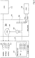
- the figure 1 shows, very schematically and in the form of blocks, an embodiment of an electronic device 100 comprising an integrated circuit 102 of the type to which the described embodiments apply, by way of example.
- the electronic device is, for example, an electronic card such as a microcircuit card, equipment for computer use, a microprocessor circuit, etc.
- the integrated circuit 102 comprises a non-volatile non-rewritable memory, of the fuse type (FUSE NV MEM) 110.
- FUSE NV MEM fuse type
- all the bits of fuse type of the memory 110 are in the same state, arbitrarily 0.
- This state corresponds, according to the native state of the fuse bits, for example, to a non-conductive or "blocked" state, of the storage elements defining the bits.
- data is stored on the non-volatile memory 110 by switching the states of (by toasting) certain bits of the memory (of memory words) to the inverse state 1, corresponding for example to a conductive or "passing" state of the corresponding storage elements.
- the integrated circuit 102 further comprises a processing unit (CPU) 112, having access to the memory 110 via an adapter 106 (WRAPPER).
- the integrated circuit 102 further comprises a JTAG (Joint Test Action Group) type access port 104 allowing a user to connect a JTAG type interface (not shown) to the circuit in order to request the running system tests.
- JTAG Joint Test Action Group
- These tests are, for example, continuity tests of the circuit detecting possible short-circuits or even tests of the logic functions of the circuit. The tests cannot be carried out during the design of prototypes, during manufacture, or even when the device 100 is returned to the manufacturer for analysis of defect(s).
- the embodiments described provide a new mechanism for authorizing access to the integrated circuit during tests, without compromising the security of this data.
- the circuit has, in particular from the point of view of the JTAG port 104, a "closed” state in which the scanning tests are blocked but in which the adapter 106 authorizes the processing unit 112 to have access to the memory 110, including its protected part (202, Fig. 2 ) containing the "secret”, and an "open” state in which scan tests are permitted, but in which the adapter 106 prohibits any access to the protected area 202 of the memory 110 to the processing unit 112 and that even through scan tests.
- the embodiments described provide for the presence of a finite state machine (FSM) 108 to control the transition from the "closed" state of the circuit to the "open” state.
- FSM finite state machine
- the adapter 106 contained in the circuit 102, ensures compatibility between data that can be entered via the JTAG interface and the data stored in the non-rewritable non-volatile memory 110.
- the adapter 106 itself contains the finite state machine 108 and is connected to the access port 104 and to the non-volatile memory 110.
- the JTAG access port 104 is not connected to the processing unit 112 and, in In particular, the respective operations of processor 112 and finite state machine 108 are independent of each other.
- figure 2 represents, schematically and in the form of blocks, more detailed than in figure 1 , an embodiment of an integrated circuit of the type to which the described embodiments apply, by way of example.
- the fuse-type non-volatile memory 110 comprises or be broken down into several distinct memory zones.
- a first zone (PROTECTED) 202 containing protected data, contains all the data (program or data proper) access to which must be reserved for operation in a secure mode or environment, that is to say when the circuit is in the closed state.
- data are stored by the end user of the circuit or by an intermediate entity between the manufacturer and this user. This data may be authentication or encryption keys, software codes or proprietary protocols, etc.
- codes or passwords are contained in dedicated memory words 204. This or these codes are in particular used to condition the reopening of the circuit.
- the code 204 is only readable by the adapter 106 and, more particularly, by the state machine 108.
- the code 204 can be stored in the zone 202 by the manufacturer during the production of the circuit 102, but is preferentially chosen and stored during the personalization phase.
- Code 204 corresponds to a fuse-like secret password which, once programmed (or locked), is only accessible by the finite state machine 108.
- the state machine 108 determines whether the chip is in an “open” state or in a “closed” state. If the chip is in a "closed” state, and if a content has been entered into a register 206 of the adapter 106 before the chip comes out of reset, the finite state machine compares the code 204 with this content. During the period in which the chip is resetting, the JTAG port 104 is functional and content can be entered and is then stored in register 206.
- the register 206 accessible via the JTAG port 104, is typically a shift register (volatile storage) written via the JTAG port and read by the state machine 108.
- the writing of the register is carried out, in the usual way, by a TDI data input being sequenced by a TCK signal from the JTAG interface.
- the function 109 of comparison between the data entered via the port 104 and those contained in the code 204 is also part of the finite state machine.
- a second area is provided in memory 110 containing first, second and third memory words 208 (WORD1), 210 (WORD2) and 212 (WORD3) having specific functions related to the opening and closing of the circuit. More particularly, each word 208, 210, 212 constitutes a counter, respectively, of the number of closures, of the number of openings and of the number of seizures of data via port 104 when the chip is reset. Initially, all the fuse bits of words 208, 210 and 212 are in the same state, arbitrarily 0. Word 210 can only be burnt out by state machine 108 (and not by unit 112).
- the length of words 208, 210 and 212 may be the same or differ from word to word. This length determines, depending on the word, the number of closings, openings and password entry attempts via the JTAG interface.
- each word 208, 210, 212 comprises at least 8 bits, preferably 32 bits.
- the bits of words 208 to 212 are irreversibly programmable bits, the corresponding counter does not count a number which can reach 2 raised to the power of the number of bits, but a number which can reach the maximum number of bits.
- the state machine 108 grids a bit (or group of bits) of the counter represented by the word 212. This uses one of the opportunities to guess the password.
- circuit 102 is locked in state "firm". For example, in the case where word 212 is made up of 8 bits (or 32 bits programmed in groups of 4 bits), the circuit is locked after eight attempts to introduce a password via the JTAG interface.
- the circuit except for the fuse-type non-volatile memory 110, can then be scanned.
- An "open” chip can be "closed” at any time by burning a bit (or group of bits) of the counter represented by word 208. This operation can be performed by the processing unit 112 or by a debugger connected to JTAG port 104.
- Closing the circuit involves frying a bit of word 208, thus using a circuit closing opportunity. If all the bits of word 208 are burned out, the circuit is stuck in the closed state and cannot be opened again.
- counters 208 and 210 are provided.
- counter 212 only prevents a password guess attack. This is useful if the 204 password is short.
- an advantage induced by the implementation of the reopenings by the state machine 108 rather than by the processing unit 112 is that reopening to perform scan tests will work even when the manufacturing defect is in the processing unit 112 itself.
- the processing unit 112 occupies a large surface of the circuit 102, in particular compared to the size of the state machine 108, and the probability that the fault having caused the malfunction of the circuit is present there is not negligible. .
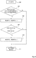
- the picture 3 is a decision tree illustrating an embodiment of a method for protecting the content of a fuse memory.
- the picture 3 is a decision tree representing the conditions under which circuit 102 is in the open state, respectively in the closed state.
- finite state machine 108 verifies the state (open or closed) in which circuit 102 is located.
- the state is determined by the values respective first, second and third words 208, 210 and 212.
- the checks of the respective counters represented by the words 208, 210 and 212 are carried out by determining the rank of the most significant bit which is at state 1. In the example of the picture 3 , it is assumed that the counters are all on the same number of bits.
- the finite state machine 108 begins by checking (block 303, WORD 1 > WORD 2?) if the value of the first word 208 is greater than the value of the second word 210. If it is the case (output Y of block 303), this means that the last operation on words 208, 210 and 212 consisted of closing circuit 102 and the state of circuit 102 therefore remains in the closed state (block 309, CLOSED ).
- output Y of block 307 this means that the maximum number of attempts to enter passwords has been reached and the circuit then remains in the closed state 309. Otherwise (output N of block 307 or of block 305, if step 307 is omitted), the state of circuit 102 is the open state (block 311, OPEN) and the test interface can send, via the shift register, the instructions required to run the circuit scan test.
- the most significant bits of the first and third words 208 and 212 must have the value 0 and the value of the second word 210 must be less than or equal to the value of the first word 208.
- steps 303, 305 and 307 of the picture 3 has no importance. In practice, these steps can be performed in parallel or independently of each other by the state machine 108 insofar as it suffices that only one of the steps gives a true result for the circuit to be in the closed state.
- the figure 4 is a flowchart representing the steps of an implementation mode of a test mode transition of an integrated circuit.
- figure 4 is a flowchart representing operations of a mode of implementing the transition from the closed state 309 (CLOSED) to a reset 301 ( picture 3 ).
- the contents of register 206 in order to detect if a password was entered via the JTAG interface during the reset, and the values of the first and third words to verify that none of them has its bit the more significant in state 1 (ie grilled).
- test request verification process ends (block 411, RUNNING TO 301) and the circuit will remain, once reset in block 301, in the closed state.
- all the bits of the fuse memory 110 are preferably at state 0. Consequently, the circuit is in the open state, which is not a problem insofar as no "secret" has been introduced in zone 202.
- An initial transition is preferentially triggered before personalizing the data supposed to remain protected and storing the code 204 in the zone 202.
- a program code executed by the processing unit causes the fusion of the least significant bit (LSB) of the word 208 (WORD1), which will place the circuit in the closed state at the next restart.
- LSB least significant bit
- WORD1 least significant bit
- a debugger connected to circuit 102 can grill the bit of word 208 of lowest order being still at state 0 to close the chip.
- the transition to the open state will be successful at the last (for example the 7 th ) entry (when the value of word 210 will reach 7). In doing so, a transition from the closed state to the open state can only occur once.
- the check performed on the most significant bit of word 208 can be replaced by a check performed on the most significant bit of word 210 (maximum number of openings reached) .
- An advantage of the described embodiments and implementations is that only finite state machine 108 can read code 204. Central processing unit 112 cannot read code 204. Thus, the circuit surface on which an attack can be performed to extract the 204 code is reduced. In other words, the re-opening of the circuit can only be performed by the finite state machine 108, and does not involve the central processing unit. Thus the surface of the circuit on which a fraudulent attack can be carried out with the aim of reopening the circuit is reduced.
- Another advantage of the embodiments and modes of implementation described is that the reopenings are executed by a finite state machine independent of the processing unit, thus allowing the detection of one or more faults which could be present on the 'processing unit.
- Another advantage of the described embodiments is that the implementation of the finite state machine requires a simple combinatorial logic that can be implemented in a robust way.
Landscapes
- Engineering & Computer Science (AREA)
- Physics & Mathematics (AREA)
- General Engineering & Computer Science (AREA)
- General Physics & Mathematics (AREA)
- Theoretical Computer Science (AREA)
- Computer Security & Cryptography (AREA)
- Software Systems (AREA)
- Semiconductor Integrated Circuits (AREA)
- Storage Device Security (AREA)
- Read Only Memory (AREA)
Applications Claiming Priority (1)
| Application Number | Priority Date | Filing Date | Title |
|---|---|---|---|
| FR2102717A FR3120953B1 (fr) | 2021-03-18 | 2021-03-18 | Protection du contenu d'une mémoire fusible |
Publications (2)
| Publication Number | Publication Date |
|---|---|
| EP4060355A1 true EP4060355A1 (de) | 2022-09-21 |
| EP4060355B1 EP4060355B1 (de) | 2023-10-04 |
Family
ID=76807705
Family Applications (1)
| Application Number | Title | Priority Date | Filing Date |
|---|---|---|---|
| EP22162199.8A Active EP4060355B1 (de) | 2021-03-18 | 2022-03-15 | Schutz des inhalts eines schmelzspeichers |
Country Status (4)
| Country | Link |
|---|---|
| US (2) | US12117487B2 (de) |
| EP (1) | EP4060355B1 (de) |
| CN (1) | CN115116533B (de) |
| FR (1) | FR3120953B1 (de) |
Families Citing this family (1)
| Publication number | Priority date | Publication date | Assignee | Title |
|---|---|---|---|---|
| FR3120953B1 (fr) * | 2021-03-18 | 2023-03-10 | St Microelectronics Grenoble 2 | Protection du contenu d'une mémoire fusible |
Citations (4)
| Publication number | Priority date | Publication date | Assignee | Title |
|---|---|---|---|---|
| US20050289355A1 (en) * | 2004-06-29 | 2005-12-29 | Dimitri Kitariev | Lockstep mechanism to ensure security in hardware at power-up |
| CN101620656A (zh) * | 2009-07-29 | 2010-01-06 | 深圳国微技术有限公司 | 安全jtag模块及保护芯片内部信息安全的方法 |
| US20120278630A1 (en) * | 2004-02-05 | 2012-11-01 | Research In Motion Limited | Debugging port security interface |
| US20190163909A1 (en) * | 2016-12-30 | 2019-05-30 | Google Llc | Secure Device State Apparatus and Method and Lifecycle Management |
Family Cites Families (18)
| Publication number | Priority date | Publication date | Assignee | Title |
|---|---|---|---|---|
| US5867505A (en) * | 1996-08-07 | 1999-02-02 | Micron Technology, Inc. | Method and apparatus for testing an integrated circuit including the step/means for storing an associated test identifier in association with integrated circuit identifier for each test to be performed on the integrated circuit |
| US6922456B2 (en) * | 2002-03-25 | 2005-07-26 | Hewlett-Packard Development Company, L.P. | Counter system and method |
| US7268577B2 (en) * | 2004-12-17 | 2007-09-11 | International Business Machines Corporation | Changing chip function based on fuse states |
| US7442583B2 (en) * | 2004-12-17 | 2008-10-28 | International Business Machines Corporation | Using electrically programmable fuses to hide architecture, prevent reverse engineering, and make a device inoperable |
| US20080320263A1 (en) * | 2007-06-20 | 2008-12-25 | Daniel Nemiroff | Method, system, and apparatus for encrypting, integrity, and anti-replay protecting data in non-volatile memory in a fault tolerant manner |
| US8405412B2 (en) * | 2009-04-28 | 2013-03-26 | Lsi Corporation | Integrated circuit self-monitored burn-in |
| US8341472B2 (en) * | 2010-06-25 | 2012-12-25 | Via Technologies, Inc. | Apparatus and method for tamper protection of a microprocessor fuse array |
| EP2856379B1 (de) * | 2012-05-30 | 2016-10-12 | Freescale Semiconductor, Inc. | Halbleiterbauelement und verfahren zur herstellung eines halbleiterbauelements |
| US9390291B2 (en) * | 2012-12-29 | 2016-07-12 | Intel Corporation | Secure key derivation and cryptography logic for integrated circuits |
| US9058903B2 (en) * | 2013-01-16 | 2015-06-16 | International Business Machines Corporation | Methods and circuits for disrupting integrated circuit function |
| US20170180131A1 (en) * | 2015-12-16 | 2017-06-22 | Intel Corporation | Secure unlock to access debug hardware |
| US10217498B2 (en) * | 2016-09-12 | 2019-02-26 | Qualcomm Incorporated | Techniques for preventing tampering with PROM settings |
| US10491401B2 (en) * | 2017-02-21 | 2019-11-26 | Google Llc | Verification of code signature with flexible constraints |
| US10481205B2 (en) * | 2017-07-27 | 2019-11-19 | Seagate Technology Llc | Robust secure testing of integrated circuits |
| US11768611B2 (en) * | 2020-04-02 | 2023-09-26 | Axiado Corporation | Secure boot of a processing chip |
| FR3120964B1 (fr) * | 2021-03-18 | 2026-03-20 | St Microelectronics Grenoble 2 | Stockage matériel d’une clé unique |
| FR3120953B1 (fr) * | 2021-03-18 | 2023-03-10 | St Microelectronics Grenoble 2 | Protection du contenu d'une mémoire fusible |
| US11615187B2 (en) * | 2021-03-31 | 2023-03-28 | Microsoft Technology Licensing, Llc | Fuse based replay protection with conservative fuse usage |
-
2021
- 2021-03-18 FR FR2102717A patent/FR3120953B1/fr active Active
-
2022
- 2022-03-15 US US17/654,918 patent/US12117487B2/en active Active
- 2022-03-15 EP EP22162199.8A patent/EP4060355B1/de active Active
- 2022-03-17 CN CN202210265421.1A patent/CN115116533B/zh active Active
-
2024
- 2024-09-12 US US18/883,619 patent/US20250004051A1/en active Pending
Patent Citations (4)
| Publication number | Priority date | Publication date | Assignee | Title |
|---|---|---|---|---|
| US20120278630A1 (en) * | 2004-02-05 | 2012-11-01 | Research In Motion Limited | Debugging port security interface |
| US20050289355A1 (en) * | 2004-06-29 | 2005-12-29 | Dimitri Kitariev | Lockstep mechanism to ensure security in hardware at power-up |
| CN101620656A (zh) * | 2009-07-29 | 2010-01-06 | 深圳国微技术有限公司 | 安全jtag模块及保护芯片内部信息安全的方法 |
| US20190163909A1 (en) * | 2016-12-30 | 2019-05-30 | Google Llc | Secure Device State Apparatus and Method and Lifecycle Management |
Also Published As
| Publication number | Publication date |
|---|---|
| CN115116533B (zh) | 2026-01-13 |
| US20220301649A1 (en) | 2022-09-22 |
| US20250004051A1 (en) | 2025-01-02 |
| FR3120953B1 (fr) | 2023-03-10 |
| US12117487B2 (en) | 2024-10-15 |
| CN115116533A (zh) | 2022-09-27 |
| EP4060355B1 (de) | 2023-10-04 |
| FR3120953A1 (fr) | 2022-09-23 |
Similar Documents
| Publication | Publication Date | Title |
|---|---|---|
| EP2280364B1 (de) | Fehlerinjektionsdetektor in einer integrierten Schaltung | |
| FR2609175A1 (fr) | Carte a circuits integres et systeme pour verifier le bon fonctionnement de la carte | |
| EP1000413A1 (de) | Chipkartenleser mit mikrokontroller und sicherheitskomponente | |
| FR2711833A1 (fr) | Circuit intégré contenant une mémoire protégée et système sécurisé utilisant ledit circuit intégré. | |
| EP4060355B1 (de) | Schutz des inhalts eines schmelzspeichers | |
| EP2313844B1 (de) | Einrichtung und verfahren zum schutz eines elektronischen systems vor unbefugtem zugang | |
| CA2104373A1 (fr) | Procede de protection d'un circuit integre contre les utilisations frauduleuses | |
| EP1724700A1 (de) | Kontrolle der Integrität eines externen Prozessorspeichers | |
| FR2670595A1 (fr) | Carte a circuit integre. | |
| CA2575143C (fr) | Procede et dispositif de traitement de donnees | |
| EP3391228B1 (de) | Verfahren zum schreiben in einem nichtflüchtigen speicher einer elektronischen einheit und zugehörige elektronische einheit | |
| EP4068134B1 (de) | Gesicherte fehlerbeseitigung | |
| Zonenberg et al. | Extraction of Secrets from 40nm {CMOS} Gate Dielectric Breakdown Antifuses by {FIB} Passive Voltage Contrast | |
| FR2889005A1 (fr) | Integrite materielle permanente des donnees | |
| FR2834366A1 (fr) | Carte a puce autoverrouillable, dispositif de securisation d'une telle carte et procedes associes | |
| EP1742407A1 (de) | Kopierschutz von digitalen Daten innerhalb einer integrierte Schaltung mit JTAG Anschluss | |
| EP1942428B1 (de) | Verfahren zur Konformitätsprüfung einer elektronischen Plattform und/oder eines Softwareprogramms auf dieser Plattform sowie entsprechende Vorrichtung und entsprechendes Computerprogramm | |
| EP1715436A2 (de) | Schutz des Ablaufs eines von einem integrierten Schaltkreis ausgeführten Programms oder von Daten, die in diesem Schaltkreis enthalten sind | |
| EP1357459B1 (de) | Gegen Umleitung gesicherter Prozessor | |
| EP1742075B1 (de) | Verfahren zum Testen eines elektronischen Schaltkreises, das einen mittels Verwendung einer Signatur gesicherten Testmodus umfasst, und zugehöriger elektronischer Schaltkreis | |
| EP0800676B1 (de) | Verfahren und einrichtung zum automatischen prüfen elektronischer bauteile | |
| EP1005686B1 (de) | Verfahren zum aufspüren von missbrauch von elektronischen telefonkarten | |
| FR2928754A1 (fr) | Carte a circuit integre ayant un programme d'exploitation modifiable et procede de modification correspondant | |
| EP1030314B1 (de) | Einrichtung und Verfahren zur Prüfung eines nichtflüchtigen wiederprogrammierbaren Speichers | |
| WO2016181062A1 (fr) | Procede de securisation d'une comparaison de donnees lors de l'execution d'un programme |
Legal Events
| Date | Code | Title | Description |
|---|---|---|---|
| PUAI | Public reference made under article 153(3) epc to a published international application that has entered the european phase |
Free format text: ORIGINAL CODE: 0009012 |
|
| STAA | Information on the status of an ep patent application or granted ep patent |
Free format text: STATUS: REQUEST FOR EXAMINATION WAS MADE |
|
| 17P | Request for examination filed |
Effective date: 20220315 |
|
| AK | Designated contracting states |
Kind code of ref document: A1 Designated state(s): AL AT BE BG CH CY CZ DE DK EE ES FI FR GB GR HR HU IE IS IT LI LT LU LV MC MK MT NL NO PL PT RO RS SE SI SK SM TR |
|
| GRAP | Despatch of communication of intention to grant a patent |
Free format text: ORIGINAL CODE: EPIDOSNIGR1 |
|
| STAA | Information on the status of an ep patent application or granted ep patent |
Free format text: STATUS: GRANT OF PATENT IS INTENDED |
|
| RIC1 | Information provided on ipc code assigned before grant |
Ipc: G01R 31/3185 20060101ALI20230601BHEP Ipc: G01R 31/317 20060101AFI20230601BHEP |
|
| INTG | Intention to grant announced |
Effective date: 20230622 |
|
| GRAS | Grant fee paid |
Free format text: ORIGINAL CODE: EPIDOSNIGR3 |
|
| GRAA | (expected) grant |
Free format text: ORIGINAL CODE: 0009210 |
|
| STAA | Information on the status of an ep patent application or granted ep patent |
Free format text: STATUS: THE PATENT HAS BEEN GRANTED |
|
| AK | Designated contracting states |
Kind code of ref document: B1 Designated state(s): AL AT BE BG CH CY CZ DE DK EE ES FI FR GB GR HR HU IE IS IT LI LT LU LV MC MK MT NL NO PL PT RO RS SE SI SK SM TR |
|
| REG | Reference to a national code |
Ref country code: GB Ref legal event code: FG4D Free format text: NOT ENGLISH |
|
| REG | Reference to a national code |
Ref country code: CH Ref legal event code: EP |
|
| REG | Reference to a national code |
Ref country code: DE Ref legal event code: R096 Ref document number: 602022000602 Country of ref document: DE |
|
| REG | Reference to a national code |
Ref country code: IE Ref legal event code: FG4D Free format text: LANGUAGE OF EP DOCUMENT: FRENCH |
|
| REG | Reference to a national code |
Ref country code: LT Ref legal event code: MG9D |
|
| REG | Reference to a national code |
Ref country code: NL Ref legal event code: MP Effective date: 20231004 |
|
| REG | Reference to a national code |
Ref country code: AT Ref legal event code: MK05 Ref document number: 1618263 Country of ref document: AT Kind code of ref document: T Effective date: 20231004 |
|
| PG25 | Lapsed in a contracting state [announced via postgrant information from national office to epo] |
Ref country code: NL Free format text: LAPSE BECAUSE OF FAILURE TO SUBMIT A TRANSLATION OF THE DESCRIPTION OR TO PAY THE FEE WITHIN THE PRESCRIBED TIME-LIMIT Effective date: 20231004 |
|
| PG25 | Lapsed in a contracting state [announced via postgrant information from national office to epo] |
Ref country code: GR Free format text: LAPSE BECAUSE OF FAILURE TO SUBMIT A TRANSLATION OF THE DESCRIPTION OR TO PAY THE FEE WITHIN THE PRESCRIBED TIME-LIMIT Effective date: 20240105 |
|
| PG25 | Lapsed in a contracting state [announced via postgrant information from national office to epo] |
Ref country code: IS Free format text: LAPSE BECAUSE OF FAILURE TO SUBMIT A TRANSLATION OF THE DESCRIPTION OR TO PAY THE FEE WITHIN THE PRESCRIBED TIME-LIMIT Effective date: 20240204 |
|
| PG25 | Lapsed in a contracting state [announced via postgrant information from national office to epo] |
Ref country code: LT Free format text: LAPSE BECAUSE OF FAILURE TO SUBMIT A TRANSLATION OF THE DESCRIPTION OR TO PAY THE FEE WITHIN THE PRESCRIBED TIME-LIMIT Effective date: 20231004 |
|
| PG25 | Lapsed in a contracting state [announced via postgrant information from national office to epo] |
Ref country code: AT Free format text: LAPSE BECAUSE OF FAILURE TO SUBMIT A TRANSLATION OF THE DESCRIPTION OR TO PAY THE FEE WITHIN THE PRESCRIBED TIME-LIMIT Effective date: 20231004 |
|
| PG25 | Lapsed in a contracting state [announced via postgrant information from national office to epo] |
Ref country code: ES Free format text: LAPSE BECAUSE OF FAILURE TO SUBMIT A TRANSLATION OF THE DESCRIPTION OR TO PAY THE FEE WITHIN THE PRESCRIBED TIME-LIMIT Effective date: 20231004 |
|
| PG25 | Lapsed in a contracting state [announced via postgrant information from national office to epo] |
Ref country code: LT Free format text: LAPSE BECAUSE OF FAILURE TO SUBMIT A TRANSLATION OF THE DESCRIPTION OR TO PAY THE FEE WITHIN THE PRESCRIBED TIME-LIMIT Effective date: 20231004 Ref country code: IS Free format text: LAPSE BECAUSE OF FAILURE TO SUBMIT A TRANSLATION OF THE DESCRIPTION OR TO PAY THE FEE WITHIN THE PRESCRIBED TIME-LIMIT Effective date: 20240204 Ref country code: GR Free format text: LAPSE BECAUSE OF FAILURE TO SUBMIT A TRANSLATION OF THE DESCRIPTION OR TO PAY THE FEE WITHIN THE PRESCRIBED TIME-LIMIT Effective date: 20240105 Ref country code: ES Free format text: LAPSE BECAUSE OF FAILURE TO SUBMIT A TRANSLATION OF THE DESCRIPTION OR TO PAY THE FEE WITHIN THE PRESCRIBED TIME-LIMIT Effective date: 20231004 Ref country code: BG Free format text: LAPSE BECAUSE OF FAILURE TO SUBMIT A TRANSLATION OF THE DESCRIPTION OR TO PAY THE FEE WITHIN THE PRESCRIBED TIME-LIMIT Effective date: 20240104 Ref country code: AT Free format text: LAPSE BECAUSE OF FAILURE TO SUBMIT A TRANSLATION OF THE DESCRIPTION OR TO PAY THE FEE WITHIN THE PRESCRIBED TIME-LIMIT Effective date: 20231004 Ref country code: PT Free format text: LAPSE BECAUSE OF FAILURE TO SUBMIT A TRANSLATION OF THE DESCRIPTION OR TO PAY THE FEE WITHIN THE PRESCRIBED TIME-LIMIT Effective date: 20240205 |
|
| PG25 | Lapsed in a contracting state [announced via postgrant information from national office to epo] |
Ref country code: SE Free format text: LAPSE BECAUSE OF FAILURE TO SUBMIT A TRANSLATION OF THE DESCRIPTION OR TO PAY THE FEE WITHIN THE PRESCRIBED TIME-LIMIT Effective date: 20231004 Ref country code: RS Free format text: LAPSE BECAUSE OF FAILURE TO SUBMIT A TRANSLATION OF THE DESCRIPTION OR TO PAY THE FEE WITHIN THE PRESCRIBED TIME-LIMIT Effective date: 20231004 Ref country code: PL Free format text: LAPSE BECAUSE OF FAILURE TO SUBMIT A TRANSLATION OF THE DESCRIPTION OR TO PAY THE FEE WITHIN THE PRESCRIBED TIME-LIMIT Effective date: 20231004 Ref country code: NO Free format text: LAPSE BECAUSE OF FAILURE TO SUBMIT A TRANSLATION OF THE DESCRIPTION OR TO PAY THE FEE WITHIN THE PRESCRIBED TIME-LIMIT Effective date: 20240104 Ref country code: LV Free format text: LAPSE BECAUSE OF FAILURE TO SUBMIT A TRANSLATION OF THE DESCRIPTION OR TO PAY THE FEE WITHIN THE PRESCRIBED TIME-LIMIT Effective date: 20231004 Ref country code: HR Free format text: LAPSE BECAUSE OF FAILURE TO SUBMIT A TRANSLATION OF THE DESCRIPTION OR TO PAY THE FEE WITHIN THE PRESCRIBED TIME-LIMIT Effective date: 20231004 |
|
| REG | Reference to a national code |
Ref country code: DE Ref legal event code: R097 Ref document number: 602022000602 Country of ref document: DE |
|
| PG25 | Lapsed in a contracting state [announced via postgrant information from national office to epo] |
Ref country code: DK Free format text: LAPSE BECAUSE OF FAILURE TO SUBMIT A TRANSLATION OF THE DESCRIPTION OR TO PAY THE FEE WITHIN THE PRESCRIBED TIME-LIMIT Effective date: 20231004 |
|
| PG25 | Lapsed in a contracting state [announced via postgrant information from national office to epo] |
Ref country code: CZ Free format text: LAPSE BECAUSE OF FAILURE TO SUBMIT A TRANSLATION OF THE DESCRIPTION OR TO PAY THE FEE WITHIN THE PRESCRIBED TIME-LIMIT Effective date: 20231004 |
|
| PG25 | Lapsed in a contracting state [announced via postgrant information from national office to epo] |
Ref country code: SK Free format text: LAPSE BECAUSE OF FAILURE TO SUBMIT A TRANSLATION OF THE DESCRIPTION OR TO PAY THE FEE WITHIN THE PRESCRIBED TIME-LIMIT Effective date: 20231004 |
|
| PG25 | Lapsed in a contracting state [announced via postgrant information from national office to epo] |
Ref country code: SM Free format text: LAPSE BECAUSE OF FAILURE TO SUBMIT A TRANSLATION OF THE DESCRIPTION OR TO PAY THE FEE WITHIN THE PRESCRIBED TIME-LIMIT Effective date: 20231004 Ref country code: SK Free format text: LAPSE BECAUSE OF FAILURE TO SUBMIT A TRANSLATION OF THE DESCRIPTION OR TO PAY THE FEE WITHIN THE PRESCRIBED TIME-LIMIT Effective date: 20231004 Ref country code: RO Free format text: LAPSE BECAUSE OF FAILURE TO SUBMIT A TRANSLATION OF THE DESCRIPTION OR TO PAY THE FEE WITHIN THE PRESCRIBED TIME-LIMIT Effective date: 20231004 Ref country code: IT Free format text: LAPSE BECAUSE OF FAILURE TO SUBMIT A TRANSLATION OF THE DESCRIPTION OR TO PAY THE FEE WITHIN THE PRESCRIBED TIME-LIMIT Effective date: 20231004 Ref country code: EE Free format text: LAPSE BECAUSE OF FAILURE TO SUBMIT A TRANSLATION OF THE DESCRIPTION OR TO PAY THE FEE WITHIN THE PRESCRIBED TIME-LIMIT Effective date: 20231004 Ref country code: DK Free format text: LAPSE BECAUSE OF FAILURE TO SUBMIT A TRANSLATION OF THE DESCRIPTION OR TO PAY THE FEE WITHIN THE PRESCRIBED TIME-LIMIT Effective date: 20231004 Ref country code: CZ Free format text: LAPSE BECAUSE OF FAILURE TO SUBMIT A TRANSLATION OF THE DESCRIPTION OR TO PAY THE FEE WITHIN THE PRESCRIBED TIME-LIMIT Effective date: 20231004 |
|
| PLBE | No opposition filed within time limit |
Free format text: ORIGINAL CODE: 0009261 |
|
| STAA | Information on the status of an ep patent application or granted ep patent |
Free format text: STATUS: NO OPPOSITION FILED WITHIN TIME LIMIT |
|
| 26N | No opposition filed |
Effective date: 20240705 |
|
| PG25 | Lapsed in a contracting state [announced via postgrant information from national office to epo] |
Ref country code: SI Free format text: LAPSE BECAUSE OF FAILURE TO SUBMIT A TRANSLATION OF THE DESCRIPTION OR TO PAY THE FEE WITHIN THE PRESCRIBED TIME-LIMIT Effective date: 20231004 |
|
| PG25 | Lapsed in a contracting state [announced via postgrant information from national office to epo] |
Ref country code: SI Free format text: LAPSE BECAUSE OF FAILURE TO SUBMIT A TRANSLATION OF THE DESCRIPTION OR TO PAY THE FEE WITHIN THE PRESCRIBED TIME-LIMIT Effective date: 20231004 |
|
| PG25 | Lapsed in a contracting state [announced via postgrant information from national office to epo] |
Ref country code: LU Free format text: LAPSE BECAUSE OF NON-PAYMENT OF DUE FEES Effective date: 20240315 |
|
| PG25 | Lapsed in a contracting state [announced via postgrant information from national office to epo] |
Ref country code: MC Free format text: LAPSE BECAUSE OF FAILURE TO SUBMIT A TRANSLATION OF THE DESCRIPTION OR TO PAY THE FEE WITHIN THE PRESCRIBED TIME-LIMIT Effective date: 20231004 |
|
| PG25 | Lapsed in a contracting state [announced via postgrant information from national office to epo] |
Ref country code: MC Free format text: LAPSE BECAUSE OF FAILURE TO SUBMIT A TRANSLATION OF THE DESCRIPTION OR TO PAY THE FEE WITHIN THE PRESCRIBED TIME-LIMIT Effective date: 20231004 Ref country code: LU Free format text: LAPSE BECAUSE OF NON-PAYMENT OF DUE FEES Effective date: 20240315 |
|
| REG | Reference to a national code |
Ref country code: BE Ref legal event code: MM Effective date: 20240331 |
|
| PG25 | Lapsed in a contracting state [announced via postgrant information from national office to epo] |
Ref country code: BE Free format text: LAPSE BECAUSE OF NON-PAYMENT OF DUE FEES Effective date: 20240331 |
|
| PG25 | Lapsed in a contracting state [announced via postgrant information from national office to epo] |
Ref country code: FR Free format text: LAPSE BECAUSE OF NON-PAYMENT OF DUE FEES Effective date: 20240331 |
|
| PG25 | Lapsed in a contracting state [announced via postgrant information from national office to epo] |
Ref country code: IE Free format text: LAPSE BECAUSE OF NON-PAYMENT OF DUE FEES Effective date: 20240315 |
|
| PG25 | Lapsed in a contracting state [announced via postgrant information from national office to epo] |
Ref country code: IE Free format text: LAPSE BECAUSE OF NON-PAYMENT OF DUE FEES Effective date: 20240315 Ref country code: FR Free format text: LAPSE BECAUSE OF NON-PAYMENT OF DUE FEES Effective date: 20240331 Ref country code: BE Free format text: LAPSE BECAUSE OF NON-PAYMENT OF DUE FEES Effective date: 20240331 |
|
| PG25 | Lapsed in a contracting state [announced via postgrant information from national office to epo] |
Ref country code: CY Free format text: LAPSE BECAUSE OF FAILURE TO SUBMIT A TRANSLATION OF THE DESCRIPTION OR TO PAY THE FEE WITHIN THE PRESCRIBED TIME-LIMIT; INVALID AB INITIO Effective date: 20220315 |
|
| PG25 | Lapsed in a contracting state [announced via postgrant information from national office to epo] |
Ref country code: FI Free format text: LAPSE BECAUSE OF FAILURE TO SUBMIT A TRANSLATION OF THE DESCRIPTION OR TO PAY THE FEE WITHIN THE PRESCRIBED TIME-LIMIT Effective date: 20231004 |
|
| REG | Reference to a national code |
Ref country code: CH Ref legal event code: H13 Free format text: ST27 STATUS EVENT CODE: U-0-0-H10-H13 (AS PROVIDED BY THE NATIONAL OFFICE) Effective date: 20251023 |
|
| PG25 | Lapsed in a contracting state [announced via postgrant information from national office to epo] |
Ref country code: TR Free format text: LAPSE BECAUSE OF FAILURE TO SUBMIT A TRANSLATION OF THE DESCRIPTION OR TO PAY THE FEE WITHIN THE PRESCRIBED TIME-LIMIT Effective date: 20231004 |
|
| PG25 | Lapsed in a contracting state [announced via postgrant information from national office to epo] |
Ref country code: CH Free format text: LAPSE BECAUSE OF NON-PAYMENT OF DUE FEES Effective date: 20250331 |
|
| PGFP | Annual fee paid to national office [announced via postgrant information from national office to epo] |
Ref country code: DE Payment date: 20260219 Year of fee payment: 5 |