EP4068502B1 - Isolant électrique - Google Patents
Isolant électrique Download PDFInfo
- Publication number
- EP4068502B1 EP4068502B1 EP20954435.2A EP20954435A EP4068502B1 EP 4068502 B1 EP4068502 B1 EP 4068502B1 EP 20954435 A EP20954435 A EP 20954435A EP 4068502 B1 EP4068502 B1 EP 4068502B1
- Authority
- EP
- European Patent Office
- Prior art keywords
- circuit
- signal
- plane
- transmission circuit
- projection
- Prior art date
- Legal status (The legal status is an assumption and is not a legal conclusion. Google has not performed a legal analysis and makes no representation as to the accuracy of the status listed.)
- Active
Links
Images


Classifications
-
- H—ELECTRICITY
- H01—ELECTRIC ELEMENTS
- H01P—WAVEGUIDES; RESONATORS, LINES, OR OTHER DEVICES OF THE WAVEGUIDE TYPE
- H01P5/00—Coupling devices of the waveguide type
- H01P5/02—Coupling devices of the waveguide type with invariable factor of coupling
-
- H—ELECTRICITY
- H01—ELECTRIC ELEMENTS
- H01P—WAVEGUIDES; RESONATORS, LINES, OR OTHER DEVICES OF THE WAVEGUIDE TYPE
- H01P1/00—Auxiliary devices
- H01P1/32—Non-reciprocal transmission devices
- H01P1/36—Isolators
- H01P1/37—Field displacement isolators
-
- H—ELECTRICITY
- H01—ELECTRIC ELEMENTS
- H01P—WAVEGUIDES; RESONATORS, LINES, OR OTHER DEVICES OF THE WAVEGUIDE TYPE
- H01P5/00—Coupling devices of the waveguide type
- H01P5/02—Coupling devices of the waveguide type with invariable factor of coupling
- H01P5/022—Transitions between lines of the same kind and shape, but with different dimensions
- H01P5/028—Transitions between lines of the same kind and shape, but with different dimensions between strip lines
-
- H—ELECTRICITY
- H01—ELECTRIC ELEMENTS
- H01P—WAVEGUIDES; RESONATORS, LINES, OR OTHER DEVICES OF THE WAVEGUIDE TYPE
- H01P1/00—Auxiliary devices
- H01P1/32—Non-reciprocal transmission devices
- H01P1/36—Isolators
Definitions
- This application relates to the field of electronic technologies, and in particular, to an electrical isolation apparatus.
- An electrical isolation apparatus is an apparatus that can be disposed between two devices and that can still transmit information between the two devices while physically isolating the two devices.
- an electrical isolation apparatus disposed between a solar panel and a control device can convert a signal with a relatively high voltage and a relatively large current that is sent by the solar panel into a signal with a relatively low voltage and a relatively small current, and then send the signal to the control device, thereby ensuring safety of the control device and safety of a person who is using the control device.
- an implementation of the electrical isolation apparatus is an optical coupler.
- a light emitting diode and a light-sensitive element are encapsulated in one package. After a signal is received on one side of the light emitting diode and the light emitting diode is energized to emit light, the light-sensitive element receives the light, generates a signal, and transmits the signal to the other side.
- Signal isolation and information transmission are implemented in an electrical-optical-electrical manner.
- this manner has disadvantages such as a limited frequency and a relatively short service life.
- Another implementation of the electrical isolation apparatus is an isolation transformer. Windings and magnetic cores are disposed. When an input winding on one side receives a signal and generates a magnetic flux, an output winding generates an electrical signal and transmits the electrical signal to the other side.
- this manner has disadvantages such as a relatively large size.
- the optical coupler is limited by a frequency and is not applicable to isolating a signal with a relatively high frequency, and the isolation transformer has a relatively large size.
- the two manners have respective disadvantages. Therefore, how to reduce a size of an electrical isolation apparatus while increasing an applicable frequency of the electrical isolation apparatus is a technical problem that needs to be resolved in the field.
- WO 2014/072335 A1 discloses a coupling structure for a galvanically separating transmission of a high frequency signal between an antenna and a sending/receiving unit, the coupling structure comprises a first reference plate arranged in a first metal layer of a multilayer printed circuit board.
- US 2017/110777 A1 discloses a flat cable high-frequency filter which includes a dielectric substrate extending in a transmission direction of a high-frequency signal.
- the dielectric substrate includes dielectric layers stacked on each other. Elongated conductor patterns are provided on a flat surface of one dielectric layer which faces another dielectric layer.
- US 8 823 216 B2 discloses a signal transmission device, in which first open-ended resonators include a first first-open-ended resonator and a second first-open-ended resonator, in which open ends of the first first-open-ended resonator face a central portion of the second first-open-ended resonator, and a central portion of the first first-open-ended resonator faces open ends of the second first-open-ended resonator.
- JP H09 232822 A discloses a high frequency coupling line which is composed of a dielectric substrate and an inductor that is formed on one surface of the dielectric substrate and is coupled to the inductor via the dielectric substrate and capacitors.
- JP 2008 067012 A discloses a high-frequency signal-transmission apparatus which transmits a high-frequency signal between circuits on different planes and comprises a resonator which has a structure wherein a part of closed-curve track is in an open/released state, or a spiral structure.
- a resonator which has a structure wherein a part of closed-curve track is in an open/released state, or a spiral structure.
- an input-output track which inputs/outputs a high-frequency signal with respect to the said resonator is formed.
- This application provides an electrical isolation apparatus.
- a signal is transmitted between a first transmission circuit, a first reference circuit, a second transmission circuit, and a second reference circuit according to a principle of electric field coupling between conductors. Therefore, in embodiments, the electrical isolation apparatus can be applied to isolation and transmission for a signal with a relatively high frequency between a first signal device and a second signal device.
- a material used by the electrical isolation apparatus may be a common metal conductor, for example, a common PCB material, which greatly reduces a size and costs of the electrical isolation apparatus, and facilitates manufacturing and implementation of the electrical isolation apparatus.
- a first aspect of this application provides an electrical isolation apparatus.
- the apparatus is connected to a first signal device through a primary stage, and is connected to a second signal device through a secondary stage.
- a first reference circuit and a first transmission circuit of the primary stage, and a second transmission circuit and a second reference circuit of the secondary stage are not in contact with each other, and are sequentially disposed in parallel to a first plane.
- a projection, on the first plane, of a second part included in the first transmission circuit overlaps with a projection of a second region of the second reference circuit on the first plane.
- a projection, on the first plane, of a fourth part included in the second transmission circuit overlaps with a projection of a fourth region of the first reference circuit on the first plane.
- the electrical isolation apparatus transmits a signal between the primary stage and the secondary stage according to a principle of electric field coupling between conductors, so that a first signal can be immediately induced to the second reference circuit to generate a corresponding second signal, regardless of a frequency of the first signal, provided that a frequency change of the first signal causes a change of positive and negative charge distribution on the first transmission circuit. Therefore, the electrical isolation apparatus provided in these embodiments can be applied to isolation and transmission for a signal with a relatively high frequency, especially an RF signal.
- the electrical isolation apparatus provided in these embodiments includes circuits in which different conductors are located, and a material used by the electrical isolation apparatus may be a common metal conductor, for example, a common PCB material may be used for implementation.
- a material used by the electrical isolation apparatus may be a common metal conductor, for example, a common PCB material may be used for implementation.
- the electrical isolation apparatus greatly reduces its size and costs, so that the electrical isolation apparatus is easy to be manufactured and implemented.
- the electrical isolation apparatus further isolates and supports, by using insulation circuits, the first reference circuit, the first transmission circuit, the second transmission circuit, and the second reference circuit that are sequentially disposed in parallel.
- a first insulation circuit may be disposed between the first reference circuit and the first transmission circuit.
- a second insulation circuit may be disposed between the first transmission circuit and the second transmission circuit.
- a third insulation circuit may be disposed between the second transmission circuit and the second reference circuit.
- the insulation circuits disposed in this embodiment can isolate and support circuits disposed in parallel at different layers, so that the circuits at the layers can be disposed in parallel and are not in direct contact with each other, thereby helping transmit a signal between the circuits not in contact through electric field coupling, and maintaining overall structural stability of the electrical isolation apparatus.
- the electrical isolation apparatus may be further connected to the first signal device and the second signal device through matching circuits, to perform impedance matching on the received first signal and second signal.
- the matching circuits are further provided on two sides of the insulation circuits disposed in this embodiment, so that a signal transmitted by the first signal device and the second signal device by using the electrical isolation apparatus, especially a high-frequency signal, can be transmitted without loss, and the signal is prevented from being reflected back to a source point. Therefore, an insertion loss caused by the electrical isolation apparatus added between the first signal device and the second signal device is reduced, and energy efficiency of signal transmission by the electrical isolation apparatus is improved.
- a shape of the second part that extends from the first transmission circuit and whose projection overlaps with the projection of the first reference circuit, and a shape of the fourth part that extends from the second transmission circuit and whose projection overlaps with the projection of the second reference circuit may be arranged as a circular shape, a rectangular shape, a ring shape, a shape of a letter L, or the like, and the shape of the second part is the same as that of the fourth part.
- the second part of the first transmission circuit and the fourth part of the second transmission circuit may be disposed in different shapes. Therefore, when the electrical isolation apparatus is used in different scenarios, the electrical isolation apparatus may be designed based on various factors such as different working conditions, circuit design requirements, and limitations on space in a device, and the shapes of the second part and the fourth part are flexibly arranged, thereby enriching application scenarios of the electrical isolation apparatus and improving application flexibility.
- materials of the first transmission circuit, the second transmission circuit, the first reference circuit, and the second reference circuit in the electrical isolation apparatus may be copper foil metal conductors; and materials of the first insulation circuit, the second insulation circuit, and the third insulation circuit disposed in the electrical isolation apparatus may be filler insulation materials.
- the transmission circuits and the reference circuits may be implemented by using the copper foil metal conductors, and the insulation circuits may be implemented by using the filler insulation materials.
- a material used by the electrical isolation apparatus is also a common material such as a conductor, which greatly reduces costs of the electrical isolation apparatus, and facilitates manufacturing and implementation of the electrical isolation apparatus.
- the metal conductors do not easily age, and do not decay with changes of time and operating environments during operating, thereby further extending a service life of the electrical isolation apparatus, improving reliability, and reducing costs caused by frequently updating the electrical isolation apparatus.
- a second aspect of this application provides an electrical isolation apparatus.
- the apparatus is connected to a first signal device through a primary stage, and is connected to a second signal device through a secondary stage.
- a first transmission circuit includes a first part and a second part.
- a projection of the first part on a first plane falls within a projection of a first return structure on the first plane.
- a projection of the second part of the first transmission circuit on the first plane overlaps with a projection of a second region of a second reference circuit on the first plane.
- a second transmission circuit includes a third part and a fourth part.
- a projection of the third part of the second transmission circuit on the first plane falls within a projection of a second return structure on the first plane.
- the first transmission circuit, the second reference circuit, the second transmission circuit, and the first reference circuit may be configured to implement signal isolation and information transmission between devices on two sides of the electrical isolation apparatus.
- the electrical isolation apparatus when transmitting a signal between the primary stage and the secondary stage according to a principle of electric field coupling between conductors, the electrical isolation apparatus provided in this embodiment can be applied to isolation and transmission for a signal with a relatively high frequency, and a size and costs of the electrical isolation apparatus are reduced. Therefore, on a basis of facilitating manufacturing and implementation of the electrical isolation apparatus, a PCB with fewer layers is used for implementation, thereby reducing structural complexity of the electrical isolation apparatus, and making implementation of the electrical isolation apparatus more flexible.
- the electrical isolation apparatus isolates and supports, by using an insulation circuit, circuits disposed in parallel at different layers.
- a fourth insulation circuit is disposed between a plane on which the first transmission circuit, the first reference circuit, and the second return circuit are located and a plane on which the second transmission circuit, the second reference circuit, and the first return circuit are located.
- the electrical isolation apparatus may be further connected to the first signal device and the second signal device through matching circuits, to perform impedance matching on a received first signal and second signal.
- a shape of the second part that extends from the first transmission circuit and whose projection overlaps with the projection of the first reference circuit, and a shape of the fourth part that extends from the second transmission circuit and whose projection overlaps with the projection of the second reference circuit may be arranged as a circular shape, a rectangular shape, a ring shape, a shape of a letter L, or the like, and the shape of the second part is the same as that of the fourth part.
- materials of the first transmission circuit, the second transmission circuit, the first reference circuit, and the second reference circuit in the electrical isolation apparatus may be copper foil metal conductors; and a material of the fourth insulation circuit disposed in the electrical isolation apparatus may be a filler insulation material.
- a signal transmission method in an embodiment of a third aspect of this application, obtains a first signal from a first signal device, inputs the first signal into a first transmission circuit and a first reference circuit, receives a second signal output by the second transmission circuit and the second reference circuit, and then sends the second signal to a second signal device.
- the first reference circuit, the first transmission circuit, the second transmission circuit, and the second reference circuit are not in contact with each other and are sequentially disposed in parallel to a first plane. There is a spacing between a projection of the first reference circuit on the first plane and a projection of the second reference circuit on the first plane.
- the first transmission circuit includes a first part and a second part.
- a projection of the first part on the first plane overlaps with a projection of a first region of the first reference circuit on the first plane.
- a projection of the second part on the first plane overlaps with a projection of a second region of the second reference circuit on the first plane.
- the second transmission circuit includes a third part and a fourth part.
- a projection of the third part on the first plane overlaps with a projection of a third region of the second reference circuit on the first plane.
- a projection of the fourth part on the first plane overlaps with a projection of a fourth region of the first reference circuit on the first plane.
- the first signal sent by the first signal device can be converted into the second signal, and then the second signal can be sent to the second signal device. Therefore, information transmission between the first signal device and the second signal device is not affected while electrical isolation is implemented between the first signal device and the second signal device.
- a signal is transmitted between the first transmission circuit, the first reference circuit, the second transmission circuit, and the second reference circuit according to a principle of electric field coupling between conductors. Therefore, this embodiment can be applied to isolation and transmission for a signal with a relatively high frequency, especially an RF signal, between the first signal device and the second signal device.
- a material used for the first transmission circuit, the first reference circuit, the second transmission circuit, and the second reference circuit configured to implement the signal transmission method in this embodiment may be a common metal conductor, for example, a common PCB material may be used for implementation, thereby greatly reducing a size and costs of the electrical isolation apparatus, and facilitating manufacturing and implementation of the electrical isolation apparatus.
- a frequency applicable to isolating the first signal device from the second signal device can be increased, and a signal can be converted by using a circuit with a relatively small size and relatively low costs.
- a first insulation circuit is further disposed between the first reference circuit and the first transmission circuit, where the first insulation circuit is parallel to the first plane, and is configured to isolate the first reference circuit from the first transmission circuit.
- a second insulation circuit is further disposed between the first transmission circuit and the second transmission circuit, where the second insulation circuit is parallel to the first plane, and is configured to isolate the first transmission circuit from the second transmission circuit.
- a third insulation circuit is further disposed between the second transmission circuit and the second reference circuit, where the third insulation circuit is parallel to the first plane, and is configured to isolate the second transmission circuit from the second reference circuit.
- the first reference circuit and the first transmission circuit are further connected to the first signal device through a first matching circuit, and the first matching circuit is configured to perform impedance matching on a signal passing through the first matching circuit.
- the second transmission circuit and the second reference circuit are further connected to the second signal device through a second matching circuit, and the second matching circuit is configured to perform impedance matching on a signal passing through the second matching circuit.
- a shape of the second part includes a circular shape, a rectangular shape, a ring shape, or a shape of a letter L; and a shape of the fourth part is the same as that of the second part.
- materials of the first transmission circuit, the second transmission circuit, the first reference circuit, and the second reference circuit are copper foil metal conductors; and materials of the first insulation circuit, the second insulation circuit, and the third insulation circuit are filler insulation materials.
- a signal transmission method in an embodiment of a fourth aspect of this application, obtains a first signal from a first signal device, inputs the first signal into a first transmission circuit and a first reference circuit, receives a second signal output by the first transmission circuit and the second reference circuit, and then sends the second signal to a second signal device.
- the first transmission circuit, the first reference circuit, and a second return circuit are disposed on a same plane.
- the second transmission circuit, the second reference circuit, and a first return circuit are disposed on a same plane.
- the first reference circuit, the first transmission circuit, the second transmission circuit, the second reference circuit, the first return circuit, and the second return circuit are not in contact with each other, and are each disposed in parallel to a first plane.
- the first transmission circuit includes a first part and a second part. A projection of the first part on the first plane falls within a projection, on the first plane, of a first return structure disposed in the first return circuit. A projection of the second part on the first plane overlaps with a projection of a second region of the second reference circuit on the first plane.
- the second transmission circuit includes a third part and a fourth part.
- a projection of the third part on the first plane falls within a projection, on the first plane, of a second return structure disposed in the second return circuit.
- a projection of the fourth part on the first plane overlaps with a projection of a fourth region of the first reference circuit on the first plane.
- the first signal sent by the first signal device can be converted into the second signal, and then the second signal can be sent to the second signal device. Therefore, information transmission between the first signal device and the second signal device is not affected while electrical isolation is implemented between the first signal device and the second signal device.
- a signal is transmitted between the first transmission circuit, the first reference circuit, the second transmission circuit, and the second reference circuit according to a principle of electric field coupling between conductors.
- this embodiment can be applied to isolation and transmission for a signal with a relatively high frequency, especially an RF signal, between the first signal device and the second signal device, thereby enriching application scenarios and avoiding a limitation by a signal frequency when a signal is being isolated and transmitted.
- a material used for the first transmission circuit, the first reference circuit, the second transmission circuit, and the second reference circuit configured to implement the signal transmission method in this embodiment may be a common metal conductor, for example, a common PCB material may be used for implementation, thereby greatly reducing a size and costs of the electrical isolation apparatus, and facilitating manufacturing and implementation of the electrical isolation apparatus.
- the method provided in this embodiment can be applied to isolation and transmission for a signal with a relatively high frequency, and a size and costs of an apparatus required for implementing the method are reduced. Therefore, on a basis of facilitating manufacturing and implementation of the apparatus on which the method provided in this embodiment is based, a PCB with fewer layers is used for implementation, thereby reducing structural complexity of the apparatus, and making implementation of the apparatus more flexible.
- a fourth insulation circuit is further disposed between a plane on which the first transmission circuit, the first reference circuit, and the second return circuit are located and a plane on which the second transmission circuit, the second reference circuit, and the first return circuit are located.
- the first reference circuit and the first transmission circuit are further connected to the first signal device through a first matching circuit, and the first matching circuit is configured to perform impedance matching on a signal passing through the first matching circuit.
- the second transmission circuit and the second reference circuit are further connected to the second signal device through a second matching circuit, and the second matching circuit is configured to perform impedance matching on a signal passing through the second matching circuit.
- a shape of the second part includes a circular shape, a rectangular shape, a ring shape, or a shape of a letter L; and a shape of the fourth part is the same as that of the second part.
- materials of the first transmission circuit, the second transmission circuit, the first reference circuit, and the second reference circuit are copper foil metal conductors; and a material of the fourth insulation circuit is a filler insulation material.
- an embodiment of this application provides a chip, including a processor and a communications interface.
- the communications interface is configured to implement communication with another device.
- the processor is configured to read instructions to implement the method according to the third aspect or the fourth aspect.
- an embodiment of this application provides a computer program product.
- the computer program product includes computer program code.
- the computer program code is executed by a computer, the computer is enabled to perform the method according to the third aspect or the fourth aspect.
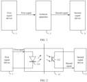
- FIG. 1 is a schematic diagram of an application scenario of this application. This application may be applied to a scenario of electrically isolating different devices, as shown in FIG. 1 .
- an electrical isolation apparatus 3 may be configured to electrically isolate a first signal device 1 from a second signal device 2.
- the electrical isolation apparatus 3 may be disposed on an electrical connection path between the first signal device 1 and the second signal device 2.
- the electrical isolation apparatus 3 converts, into a second signal with a relatively small current or a relatively low voltage, the first signal that is output by the first signal device 1 and that has a relatively large current or a relatively high voltage, and outputs the second signal to the second signal device 2.
- the disposed electrical isolation apparatus 3 may process the first signal sent by the first signal device 1, and then send a processed signal to the second signal device 2, to prevent the first signal from being directly transmitted from the first signal device 1 to the second signal device 2, and relieve a safety hazard posed by the first signal to the second signal device 2.
- the electrical isolation apparatus 3 does not directly transmit the first signal from the first signal device 1 to the second signal device 2, energy, information, or the like carried in the first signal may still be transmitted to the second signal device 2 by using the second signal obtained through processing by the electrical isolation apparatus 3. Therefore, normal communication between the first signal device 1 and the second signal device 2 is not affected while a safety hazard is relieved.
- the electrical isolation apparatus shown in FIG. 1 may be applied to a situation in which currents and voltages of signals processed by two devices are different, or the two devices are connected to different ground potentials, but information still needs to be exchanged between the two devices.
- the electrical isolation apparatus may be disposed between the two devices. In this way, information can be exchanged between the two independent devices while direct signal transmission is avoided to ensure safety of the devices and personnel.
- an electrical signal generated by a solar panel from sunlight is transmitted to a power grid to generate power.
- a photovoltaic power generating operator may use a control device, such as a mobile phone or a computer, to obtain a working status of the solar panel, adjust a working parameter of the solar panel, and the like, to meet an intelligent control requirement of the operator.
- the electrical signal output by the solar panel has an excessively high voltage.
- an electrical isolation apparatus may be disposed between the solar panel and the device, so that a first signal that is output by the solar panel and that has a relatively high voltage may be converted into a second signal with a relatively low voltage, and then the second signal is sent to the device used by the operator.
- FIG. 2 is a schematic diagram of a structure of an electrical isolation apparatus, and shows a manner of disposing the electrical isolation apparatus 3 shown in FIG. 1 when the electrical isolation apparatus 3 is an optical coupler (optical coupler, OC) 31.
- a light emitter 311 for example, an infrared light emitting diode LED
- a light receiver 312 for example, a light sensitive semiconductor transistor or a light sensitive resistor
- the light emitter emits light when a signal passes through the light emitter, and the light receiver generates a photocurrent after receiving the light, thereby implementing "electrical-optical-electrical" conversion.
- FIG. 1 optical coupler
- FIG. 2 is a schematic diagram of a structure of an electrical isolation apparatus, and shows a manner of disposing the electrical isolation apparatus 3 shown in FIG. 1 when the electrical isolation apparatus 3 is an optical coupler (optical coupler, OC) 31.
- a light emitter 311 for example, an infrared light emitting diode LED
- an input end of the optical coupler 31, that is, the light emitter 311, is connected to the first signal device 1; and an output end of the optical coupler 31, that is, the light receiver 312, is connected to the second signal device 2.
- the light emitter 311 converts the electrical signal into an optical signal to emit light.
- the light receiver 312 outputs a second signal to the second signal device 2.
- the first signal and the second signal are independent of each other, and voltages of the first signal and the second signal may be different.
- the optical coupler 31 implements signal isolation and information transmission between devices on two sides.
- the optical coupler shown in FIG. 2 is relatively widely used, the optical coupler has the following obvious disadvantages: First, a conversion rate between the light emitter and the light receiver in the optical coupler has an upper limit. As a result, the optical coupler can be used to transmit only a first signal whose frequency is less than 10 MHz. For a first signal with a higher frequency, the first signal cannot be converted into a second signal at a higher conversion rate. In addition, costs of an optical coupler with a higher conversion rate are higher. Therefore, the optical coupler is usually used only in a scenario of isolating a low-frequency signal at a high voltage.
- a service life of the diode disposed in the optical coupler is relatively short, and light emitting efficiency of the diode decays with changes of time and operating environments, thereby reducing a service life of the optical coupler, and reducing reliability.
- the optical coupler can perform only unidirectional signal transmission in a direction from the light emitter to the light receiver. Therefore, bidirectional signal transmission cannot be implemented between devices connected to two sides of the optical coupler.
- FIG. 3 is a schematic diagram of a structure of another electrical isolation apparatus, and shows a manner of disposing the electrical isolation apparatus 3 shown in FIG. 1 when the electrical isolation apparatus 3 is an isolation transformer 32.
- An input winding N1 of the isolation transformer 32 is connected to the first signal device 1, and an output winding N2 is connected to the second signal device 2.
- the first signal when a first signal output by the first signal device 1 passes through the input winding N1, the first signal generates a magnetic flux ⁇ in a magnetic core according to Faraday's law of electromagnetic induction.
- the magnetic flux ⁇ in the same magnetic core causes the output winding N2 to output a second signal to the second signal device 2, thereby implementing "electrical-magnetic-electrical" conversion.
- the first signal and the second signal can be independent of each other, and voltages of the first signal and the second signal may be different, thereby implementing signal isolation and information transmission between devices on two sides, and implementing isolation for a signal with a relatively high frequency.
- the isolation transformer shown in FIG. 3 also has the following disadvantages: First, the isolation transformer usually has a relatively large size, and the size increases with an increase in a voltage difference between input and output signals, thereby causing inconvenience to disposing and engineering implementation. Second, the isolation transformer is not applicable to isolating a high-frequency signal either. To implement safety isolation, a signal attenuation is relatively large.
- the high-frequency signal may be at least a radio frequency (radio frequency, RF) signal within a frequency range of 300 kHz to 300 GHz.
- FIG. 4 is a schematic diagram of a structure of an embodiment of an electrical isolation apparatus according to this application.
- the electrical isolation apparatus 33 provided in this embodiment is disposed between a first signal device 1 and a second signal device 2.
- the electrical isolation apparatus 33 may convert the first signal into a second signal and output the second signal to the second signal device 2.
- the electrical isolation apparatus 33 may convert the third signal into a fourth signal and output the fourth signal to the first signal device 1.
- the electrical isolation apparatus provided in this embodiment may implement bidirectional transmission.
- a principle of the electrical isolation apparatus 33 is described by using unidirectional transmission as an example in which the first signal device 1 sends the first signal to the electrical isolation apparatus 33, and the electrical isolation apparatus 33 outputs the second signal to the second signal device 2.
- the first signal device 1 includes a first terminal 11 and a second terminal 12 that may be configured to send/receive an alternating current signal.
- the first signal device 1 may output a forward current to the electrical isolation apparatus 33 through the first terminal 11 of the first signal device 1, and a current returns through the second terminal 12.
- the first signal device 1 may output a forward current to the electrical isolation apparatus 33 through the second terminal 12 of the first signal device 1, and a current returns through the first terminal 11.
- the second signal device 2 includes a first terminal 21 and a second terminal 22 that may be configured to send/receive an alternating current signal.
- the second signal device 2 may output a forward current to the electrical isolation apparatus 33 through the first terminal 21 of the second signal device 2, and a current returns through the second terminal 22.
- the second signal device 2 may output a forward current to the electrical isolation apparatus 33 through the second terminal 22 of the second signal device 2, and a current returns through the first terminal 21.
- the electrical isolation apparatus 33 provided in this embodiment includes a primary stage 331 and a secondary stage 332.
- the primary stage 331 is connected to the first signal device 1, and the secondary stage 332 is connected to the second signal device 2.
- the primary stage 331 and the secondary stage 332 are disposed independently and are not in contact with each other.
- the primary stage 331 includes a first transmission circuit 3311 and a first reference circuit 3312.
- the two circuits are connected to the two terminals of the first signal device 1 in a one-to-one correspondence.
- the first transmission circuit 3311 is connected to the first terminal 11 of the first signal device 1
- the first reference circuit 3312 is connected to the second terminal 12 of the first signal device 1.
- the secondary stage 332 includes a second transmission circuit 3321 and a second reference circuit 3322.
- the two circuits are connected to the two terminals of the second signal device 2 in a one-to-one correspondence.
- the second transmission circuit 3321 is connected to the first terminal 21 of the second signal device
- the second reference circuit 3322 is connected to the second terminal 22 of the second signal device.
- FIG. 5 is a schematic diagram of a hierarchical structure of the electrical isolation apparatus according to this application.
- the first reference circuit 3312, the first transmission circuit 3311, the second transmission circuit 3321, and the second reference circuit 3322 are not in contact with each other, and are sequentially disposed in parallel to one plane (denoted as a first plane) from top to bottom in the figure.
- an insulation circuit may be disposed between two adjacent circuits of the four circuits that are not in contact with each other, to isolate different circuits.
- a first insulation circuit 3313 is disposed between the first reference circuit 3312 and the first transmission circuit 3311
- a second insulation circuit 333 is disposed between the first transmission circuit 3311 and the second transmission circuit 3321
- a third insulation circuit 3323 is disposed between the second transmission circuit 3321 and the second reference circuit 3322.
- the first insulation circuit 3313, the second insulation circuit 333, and the third insulation circuit 3323 are also disposed in parallel to the first plane.
- each insulation circuit may be configured to isolate circuits disposed on two sides, and the insulation circuit may be in contact with the circuits disposed on the two sides.
- first reference circuit 3312, the first transmission circuit 3311, the second transmission circuit 3321, and the second reference circuit 3322 provided in this embodiment are all disposed in parallel to the first plane, projections of these circuits on the first plane do not exactly overlap.
- FIG. 6 to FIG. 10 the following describes space arrangement requirements that at least need to be met by the first reference circuit 3312, the first transmission circuit 3311, the second transmission circuit 3321, and the second reference circuit 3322 in the electrical isolation apparatus provided in this embodiment.
- the electrical isolation apparatus provided in this embodiment should meet all of the following three arrangement requirements.
- FIG. 6 is a schematic diagram of a projection of a reference circuit according to this application.
- shapes of the first reference circuit 3312 and the second reference circuit 3322 are a rectangular shape.
- the shapes of the foregoing two reference circuits are not limited in this application, and may be alternatively another shape such as a circular shape or a triangular shape.
- a plane on which the second insulation circuit 333 between the first reference circuit 3312 and the second reference circuit 3322 is located serves as a base plane of the first plane. In this case, in FIG.
- a projection of the first reference circuit 3312 on the first plane overlaps with a region A of the second insulation circuit 333
- a projection of the second reference circuit 3322 on the first plane overlaps with a region B of the second insulation circuit 333. It can be learned that the region A and the region B have no overlapping part, and a region C between an edge a of the region A and an edge b of the region B separates the region A from the region B.
- Arrangement requirement 2 Projections of the first transmission circuit 3311 and the second transmission circuit 3321 on the first plane have no overlapping region.
- Projection of a part of the first transmission circuit 3311 and the first reference circuit 3312 have an overlapping region
- projection of a part of the first transmission circuit 3311 and the second reference circuit 3322 have an overlapping region
- projection of a part of the second transmission circuit 3321 and the second reference circuit 3322 have an overlapping region
- projection of a part of the second transmission circuit 3321 and the first reference circuit 3312 have an overlapping region.
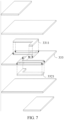
- FIG. 7 is a schematic diagram of a projection of a transmission circuit according to this application.
- shapes of the first transmission circuit 3311 and the second transmission circuit 3321 are an "L shape".
- the shapes of the foregoing two transmission circuits are not limited in this application, and may be alternatively another shape such as a circular shape, a triangular shape, or a ring shape.
- a plane on which the second insulation circuit 333 is located serves as a base plane of the first plane. In this case, in FIG.
- a projection of the first transmission circuit 3311 on the first plane overlaps with a part of a region A (a projection of the first reference circuit 3312 on the first plane), a part of a region B (a projection of the second reference circuit 3322 on the first plane), and a part of a region C of the second insulation circuit 333.
- a projection of the second transmission circuit 3321 on the first plane also overlaps with a part of the region A, a part of the region B, and a part of the region C of the second insulation circuit 333.
- FIG. 8 is a schematic diagram of division of different parts of a transmission circuit according to this application
- FIG. 9 is a schematic diagram of division of different regions of a reference circuit according to this application.
- the first transmission circuit 3311 may be divided into a first part and a second part.
- a projection of the first part on the first plane overlaps with a projection, on the first plane, of a first region of the first reference circuit 3312 shown in FIG. 9 .
- a projection of the second part on the first plane overlaps with a projection, on the first plane, of a second region of the second reference circuit 3322 shown in FIG. 9 .
- the second transmission circuit 3321 may be divided into a third part and a fourth part.
- a projection of the third part on the first plane overlaps with a projection, on the first plane, of a third region of the second reference circuit 3322 shown in FIG. 9 .
- a projection of the fourth part on the first plane overlaps with a projection, on the first plane, of a fourth region of the first reference circuit 3312 shown in FIG. 9 .
- FIG. 10 is a schematic diagram of a structure of a cross section of the electrical isolation apparatus according to this application, and shows a cross section of the electrical isolation apparatus observed from an L direction shown in FIG. 5 .
- the first insulation circuit 3313 extends beyond ends of the first reference circuit 3312 and the first transmission circuit 3311 that are disposed on two sides of the first insulation circuit 3313, and is disposed between the first transmission circuit 3311 and the first reference circuit 3312. Therefore, the first reference circuit 3312 and the first transmission circuit 3311 can be completely isolated physically, without parts in direct contact or facing each other.
- the first insulation circuit 3313 is configured to support the first transmission circuit 3311 and the first reference circuit 3312.
- the second insulation circuit 333 extends beyond ends of the first transmission circuit 3311 and the second transmission circuit 3321 that are disposed on two sides of the second insulation circuit 333, and is disposed between the first transmission circuit 3311 and the second transmission circuit 3321. Therefore, the first transmission circuit 3311 and the second transmission circuit 3321 can be completely isolated physically, without parts in direct contact or facing each other.
- the second insulation circuit 333 is configured to support the first transmission circuit 3311 and the second transmission circuit 3321.
- the third insulation circuit 3323 extends beyond ends of the second transmission circuit 3321 and the second reference circuit 3322 that are disposed on two sides of the third insulation circuit 3323, and is disposed between the second transmission circuit 3321 and the second reference circuit 3322. Therefore, the second transmission circuit 3321 and the second reference circuit 3322 can be completely isolated physically, without parts in direct contact or facing each other.
- the third insulation circuit 3323 is configured to support the second transmission circuit 3321 and the second reference circuit 3322. In addition, it can be learned from the cross-sectional view shown in FIG.
- a length of the first part of the first transmission circuit 3311 that extends to the second reference circuit 3322 is N, and a length of the third part of the second transmission circuit 3321 that extends to the first reference circuit 3312 is M.
- FIG. 11 is a schematic diagram of a principle of electric field coupling in the electrical isolation apparatus according to this application.
- Coupling refers to a process of transmitting a signal from one stage to another stage.
- the electric field coupling means that an interactive electric field is generated between two overlapping conductors under an action of a high-frequency alternating current, and a "displacement current" is generated between the two conductors under an action of the interactive electric field, to transmit energy between the two conductors.
- a conductor X and a conductor Y are disposed in parallel and opposite to each other.
- FIG. 12 is a schematic diagram of an operating principle of the electrical isolation apparatus according to this application, and shows a specific operating principle of performing, by the electrical isolation apparatus shown in FIG. 5 , electrical isolation between a first signal device and a second signal device according to the principle of electric field coupling shown in FIG. 11 .
- a first signal sent by the first signal device to the electrical isolation apparatus 33 through a first port 11 and a second port 12 of the first signal device is denoted as an alternating current signal within a voltage range of -V1 to +V1.
- the first signal device 1 In a positive half-cycle of the alternating current signal of the first signal, for example, in a time period of t0 to 11, the first signal device 1 outputs a current signal in a forward direction to the first transmission circuit 3311 of the electrical isolation apparatus 33 through the first port 11 of the first signal device 1, so that positive charges are distributed on the first transmission circuit 3311.
- the first part of the first transmission circuit 3311 and the first region of the first reference circuit 3312 constitute a return circuit, and the current signal successively passes through the first part and the first region to return to the second port 12 of the first signal device.
- the positive charges distributed on the second part cause negative charges to be generated in the second region through electric field coupling shown in FIG. 11 .
- the negative charges distributed on the second reference circuit 3322 in which the second region is located further cause positive charges to be generated on the second transmission circuit 3321
- the third part of the second transmission circuit 3321 and the third region of the second reference circuit 3322 can further constitute a return circuit, to generate a second signal to be transmitted to the second signal device 2.
- a current direction of the second signal is as follows: A current signal in a forward direction is output from a first port 21 of the second signal device 2, and the current signal successively passes through the third part of the second transmission circuit 3321 and the third region of the second reference circuit 3322 to return to a second port 22 of the second signal device 2.
- the first signal device In a negative half-cycle of the alternating current signal of the first signal, for example, in a time period of t1 to 12, the first signal device outputs a current signal in a forward direction to the first reference circuit 3311 through the second port 12.
- the first part of the first transmission circuit 3311 and the first region of the first reference circuit 3312 constitute a return circuit, and the current signal successively passes through the first region and the first part to return to the first port 11 of the first signal device, so that negative charges are distributed on the first transmission circuit 3311.
- the negative charges distributed on the second part cause positive charges to be generated in the second region through electric field coupling shown in FIG. 11 .
- a current direction of the second signal is as follows: A current signal in a forward direction is output from the second port 22 of the second signal device 2, and the current signal successively passes through the third region of the second reference circuit 3322 and the third part of the second transmission circuit 3321 to return to the first port 21 of the second signal device 2.
- the second signal device can be enabled to receive an alternating current signal within a voltage range of -V2 to +V2.
- the first signal and the second signal are current signals
- the first signal device 1 and the second signal device 2 provide voltages for the current signals through power supplies and ground ports respectively disposed in the first signal device 1 and the second signal device 2.
- a voltage provided by the first signal device is V1
- a voltage of the first signal sent by the first signal device ranges from -V1 to V1
- a voltage provided by the second signal device is V2
- a voltage of the second signal received by the second signal device ranges from -V2 to V2.
- the electrical isolation apparatus 33 converts the first signal received by the primary stage into the second signal at the secondary stage. This is equivalent to that the change regularity of the alternating current of the first signal is transmitted from the primary stage to the secondary stage, so that phase changes of the first signal and the second signal are the same. Amplitudes may be related to voltages provided by the first signal device and the second signal device.
- the voltage V2 of the second signal and the voltage V1 of the first signal may be the same or different.
- the power supplies that are disposed in the first signal device and the second signal device and that provide voltages are not limited in this application.
- a power supply of the first signal device 1 can provide a voltage between the first port 11 and the second port 12 of the first signal device 1
- a power supply of the second signal device 2 can provide a voltage between the first port 21 and the second port 22 of the second signal device 2.
- a voltage of a first signal sent by a solar panel is relatively high, and may usually reach hundreds of volts (greater than 100 V).
- a phase of a second signal sent to a control device is the same as that of the first signal but a voltage may be several volts (less than 10 V) provided by the control device, a safety hazard caused by transmitting the first signal with a relatively high voltage to the second signal device is avoided.
- information such as a change regularity of the first signal may be transmitted to the second signal device by using the second signal with a relatively low voltage, so that the second signal device can still receive the information in the first signal sent by the first signal device.
- the electrical isolation apparatus may also send a fourth signal to the first signal device through electric field coupling.
- An implementation and an implementation principle thereof are the same as those in the embodiment in which the first signal sent by the first signal device is converted by the electrical isolation apparatus into the second signal to be sent to the second signal device. Details are not described again.
- the electrical isolation apparatus can further output the fourth signal to the first signal device after converting the third signal sent by the second signal device.
- the third signal and the fourth signal may also have a same phase change, and amplitudes may be the same or different.
- lengths of the first transmission circuit 3311 and the second transmission circuit 3321 may be set based on a wavelength of a processed signal, and the lengths of the first transmission circuit 3311 and the second transmission circuit 3321 are directly proportional to the wavelength.
- a length of the first transmission circuit 3311 is a length of an entire "L" shape, and the length of the first transmission circuit 3311 is directly proportional to a wavelength of the first signal
- a length of the second transmission circuit 3321 is a length of an entire "L" shape, and the length of the second transmission circuit 3321 is directly proportional to a wavelength of the third signal.
- the electrical isolation apparatus provided in this embodiment is connected to the first signal device through the primary stage, and is connected to the second signal device through the secondary stage. After the first signal sent by the first signal device is received, the first part, of the first transmission circuit of the primary stage, that extends to the secondary stage, and the first region of the second reference circuit of the secondary stage may be configured to jointly generate the second signal and send the second signal to the second signal device. After the third signal sent by the second signal device is received, the third part, of the second transmission circuit of the secondary stage, that extends to the primary stage, and the third region of the first reference circuit of the primary stage may be configured to jointly generate the fourth signal and send the fourth signal to the first signal device. Therefore, the electrical isolation apparatus provided in this embodiment has at least the following technical effects.
- the electrical isolation apparatus provided in this embodiment transmits a signal between the primary stage and the secondary stage according to a principle of electric field coupling between conductors, so that a first signal can be immediately induced to the second reference circuit to generate a corresponding second signal, regardless of a frequency of the first signal, provided that a frequency change of the first signal causes a change of positive and negative charge distribution on the first transmission circuit. Therefore, the electrical isolation apparatus provided in this embodiment can be applied to isolation and transmission for a signal with a relatively high frequency, especially an RF signal. Therefore, compared with the technologies shown in FIG. 2 and FIG. 3 , this embodiment enriches application scenarios of the electrical isolation apparatus, so that signal isolation and transmission are not limited by a signal frequency.
- the electrical isolation apparatus includes circuits in which different conductors are located, and a material used by the electrical isolation apparatus may be a common metal conductor, for example, a common PCB material may be used for implementation.
- a material used by the electrical isolation apparatus may be a common metal conductor, for example, a common PCB material may be used for implementation.
- the electrical isolation apparatus greatly reduces its costs, so that the electrical isolation apparatus is easy to be manufactured and implemented.
- a signal can be transmitted by using a conductor in a circuit in this embodiment, compared with a device, such as the optical coupler shown in FIG. 2 , whose service life is reduced due to a limitation by a service life of a diode, a metal conductor does not easily age, and does not decay with changes of time and operating environments during operating, thereby further extending a service life of the electrical isolation apparatus, improving reliability, and reducing costs caused by frequently updating the electrical isolation apparatus.
- the electrical isolation apparatus can effectively reduce its size, so that flexibility of disposing the electrical isolation apparatus is improved.
- the electrical isolation apparatus isolates a signal between the first signal device and the second signal device.
- the primary stage and the secondary stage can be understood as being symmetrically disposed, bidirectional signal transmission between the first signal device and the second signal device can be implemented.
- the electrical isolation apparatus enriches its functions, so that usage efficiency of the electrical isolation apparatus is improved.
- phase of input and output signals are the same, so that a 0-degree phase shift can be achieved for the input and output signals.
- the electrical isolation apparatus can also be used, and can ensure stable phases without shifts, thereby enriching application scenarios of the electrical isolation apparatus.
- a "cross" coupling manner is used for the electrical isolation apparatus provided in this embodiment.
- the first transmission circuit of the primary stage serves as a signal (signal) terminal and is coupled to the second transmission circuit of the secondary stage that serves as a ground (GND) terminal
- the second transmission circuit of the secondary stage serves as a signal (signal) terminal and is coupled to the first transmission circuit of the primary stage that serves as a ground (GND) terminal.
- this manner is more flexible in design, and an insertion loss caused between the first signal device and the second signal device by disposing the electrical isolation apparatus can be further reduced.
- FIG. 13 is a schematic diagram of a structure of an embodiment of an electrical isolation apparatus according to this application.
- a first matching circuit 41 and a second matching circuit 42 are further included in the embodiment shown in FIG. 13 .
- the first matching circuit 41 is disposed between the first signal device 1 and the primary stage 331 of the electrical isolation apparatus 33, and is configured to perform impedance matching on a signal passing through the first matching circuit 41.
- the second matching circuit 42 is disposed between the second signal device 2 and the secondary stage 332 of the electrical isolation apparatus 33, and is configured to perform impedance matching on a signal passing through the second matching circuit 42.
- the impedance refers to an obstruction function performed by a current in a transmission circuit.
- the impedance matching is performed on the transmission circuit.
- a matching unit is used to make the impedance on the transmission circuit continuous, so that all signals at a transmit end can be transmitted to a receive end, and no signal is reflected back to the transmit end, thereby improving energy efficiency of the signals.
- the first matching circuit 41 may be configured to perform signal impedance matching with a standard impedance of 50 ⁇ on the first port 11 and the second port 12 of the first signal device 1, and the second matching circuit 42 may be configured to perform impedance matching with a standard impedance of 50 ⁇ on the first port 21 and the second port 22 of the second signal device 2.
- RF radio frequency
- first matching circuit 41 and the second matching circuit 42 may be the same or different, and available matching circuits include: matching through printed circuit board (printed circuit boards, PCB) wiring, matching by using discrete resistor-capacitor devices, and the like.
- FIG. 14 is a schematic diagram of another shape of a transmission circuit according to this application.
- a shape of the second part, of the first transmission circuit 3311, that extends to the secondary stage may be another shape such as a rectangular shape, a ring shape, or a circular shape.
- a shape of the fourth part, of the second transmission circuit 3322, that extends to the primary stage is the same as the shape of the second part, and for example, may also be another shape such as a rectangular shape, a ring shape, or a circular shape.
- materials of the first transmission circuit 3311, the second transmission circuit 3321, the first reference circuit 3312, and the second reference circuit 3322 may be copper foil metal conductors.
- materials of the first insulation circuit 3313, the second insulation circuit 333, and the third insulation circuit 3323 may be filler insulation materials whose model is FR4 (a code of a fire-resistant material class), air, plastic, or the like.
- An insulation circuit may be disposed to prevent discharge, creepage, and the like between conductors on two sides of the insulation circuit.
- a non-conducting insulation material may prevent voltage breakdown between conductors on two sides, and ensure physical isolation between the conductors on the two sides.
- the foregoing insulation circuits may further serve as support structures for the entire electrical isolation apparatus, and provide integral support for the entire apparatus.
- FIG. 15 is a structural diagram of specific engineering application of the electrical isolation apparatus according to this application.
- FIG. 15 shows a specific application manner of the electrical isolation apparatus 33 in a radio frequency communications system.
- the electrical isolation apparatus 33 shown in FIG. 15 is specifically implemented by a PCB.
- a designed pass-band center frequency of the electrical isolation apparatus 33 is 2.4 GHz.
- the first port 11 is further disposed at the primary stage of the electrical isolation apparatus 33, and is configured to connect to the first signal device 1.
- the first signal device 1 may be connected to a radio frequency IC device and a transceiver antenna, and the first port may be an IPEX terminal.
- both the first port 11 and the second port 12 may be IPEX terminals.
- the IPEX terminals may be disposed at a surface layer of the PCB, and the first matching circuit 41 and the second matching circuit 42 may also be disposed at the surface layer of the PCB.
- a memory signal may be connected to an inner-layer coupling conductor through a via, so that inner-layer signal coupling can be implemented, and direct current (direct current, DC) withstand voltage safety isolation at a KV (a voltage level) level can be achieved.
- the provided electrical isolation apparatus may be implemented by a four-layer (layer) PCB (the first transmission circuit, the first reference circuit, the second transmission circuit, and the second reference circuit are respectively disposed at different layers, and there are four layers in total).
- this application further provides another electrical isolation apparatus. Signal isolation and information transmission may be performed by using the same principle of electric field coupling, and fewer PCB layers may be used for implementation.
- FIG. 16 is a schematic diagram of a structure of an embodiment of an electrical isolation apparatus according to this application.
- a primary stage of the electrical isolation apparatus includes a first transmission circuit 3311, a first reference circuit 3312, and a first return circuit 3314.
- a secondary stage includes a second transmission circuit 3321, a second reference circuit 3322, and a second return circuit 3324.
- the first transmission circuit 3311, the first reference circuit 3312, and the second return circuit 3324 are disposed on a same plane, that is, an uppermost plane in FIG. 16 .
- the second transmission circuit 3321, the second reference circuit 3322, and the first return circuit 3314 are disposed on a same plane, that is, a lowermost plane in FIG. 16 .
- a fourth insulation circuit 3331 may be further disposed between the primary stage and the secondary stage, and is configured to isolate and support a plane on which the first transmission circuit 3311, the first reference circuit 3312, and the second return circuit 3324 are located, and a plane on which the second transmission circuit 3321, the second reference circuit 3322, and the first return circuit 3314 are located.
- first transmission circuit 3311, the first reference circuit 3312, the first return circuit 3314, the second transmission circuit 3321, the second reference circuit 3322, and the second return circuit 3324 are not in contact with each other, and are disposed in parallel to one plane (denoted as a first plane).
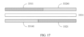
- FIG. 17 is a schematic diagram of a structure of a cross section of the electrical isolation apparatus according to this application.
- the first transmission circuit 3311 includes a first part and a second part.
- the first part is disposed directly above a first return structure 33141 disposed in the first return circuit 3314.
- a projection of the first part on the first plane falls within a projection of the first return structure 33141 on the first plane.
- a projection of the second part of the first transmission circuit 3311 on the first plane overlaps with a projection of a second region of the second reference circuit 3322 on the first plane.
- the second transmission circuit 3321 includes a third part and a fourth part.
- the third part is disposed directly below a second return structure 33241 disposed in the second return circuit 3324.
- a projection of the third part on the first plane falls within a projection of the second return structure 33241 on the first plane.
- a projection of the fourth part of the second transmission circuit 3321 on the first plane overlaps with a projection of a fourth region of the first reference circuit 3312 on the first plane.
- the first transmission circuit 3311, the second reference circuit 3322, the second transmission circuit 3321, and the first reference circuit 3312 may be configured to implement signal isolation and information transmission between devices on two sides of the electrical isolation apparatus.
- the first transmission circuit 3311 and the first reference circuit 3312 are connected to a first signal device
- the second transmission circuit 3321 and the second reference circuit 3322 are connected to a second signal device
- a first signal sent by the first signal device is transmitted through the first transmission circuit 3311 and the first reference circuit 3312 (transmission is performed through electric field coupling on a plane on which the first transmission circuit 3311 overlaps with the projection of the first reference circuit 3312).
- transmission is performed through electric field coupling on a plane on which the first transmission circuit 3311 overlaps with the projection of the first reference circuit 3312.
- the second transmission circuit 3321 and the second reference circuit 3322 can further constitute a return circuit (transmission is performed through electric field coupling on a plane on which the second transmission circuit 3321 overlaps with the projection of the second reference circuit 3322), to generate a second signal to be transmitted to the second signal device 2.
- the first return circuit 3314 is further disposed below the first transmission circuit 3311 in FIG. 16 .
- the first return structure 33141 disposed in the first return circuit 3314 provides a reference plane for the first transmission circuit 3311.
- the first transmission circuit 3311 may be connected to the first return structure 33141 through a via provided in the fourth insulation circuit 3331.
- the second return circuit 3324 is further disposed above the second transmission circuit 3321 in FIG. 16 .
- the second return structure 33241 disposed in the second return circuit 3324 provides a reference plane for the second transmission circuit 3321.
- the reference plane may be a reference ground plane.
- the second transmission circuit 3321 may be connected to the second return structure 33241 through a via provided in the fourth insulation circuit 3331.
- the first return structure 33141 and the second return structure 33241 may be connected (a connection relationship is not shown in the figure), to provide a same reference plane for the primary stage and the secondary stage of the electrical isolation apparatus.
- the negative charges distributed on the second part cause positive charges to be generated in the second region through electric field coupling shown in FIG. 11 .
- the positive charges distributed on the second reference circuit 3322 in which the second region is located further cause negative charges to be generated on the second transmission circuit 3321.
- the second transmission circuit 3321 and the second reference circuit 3322 can further constitute a return circuit (transmission is performed through electric field coupling on a plane on which the second transmission circuit 3321 overlaps with the projection of the second reference circuit 3322), to generate a second signal to be transmitted to the second signal device 2.
- the electrical isolation apparatus may also send a fourth signal to the first signal device through electric field coupling.
- An implementation and an implementation principle thereof are the same as those in the embodiment in which the first signal sent by the first signal device is converted by the electrical isolation apparatus into the second signal to be sent to the second signal device. Details are not described again.
- the electrical isolation apparatus provided in this embodiment is implemented by a PCB with fewer layers on a basis of keeping a technical principle and a technical effect same as those in FIG. 5 to FIG. 15 , thereby reducing structural complexity of the electrical isolation apparatus, and making implementation of the electrical isolation apparatus more flexible and effective.
- a structure of the electrical isolation apparatus is described in detail.
- another electronic device may also implement information transmission through software while isolating a signal.
- this application provides a signal transmission method that may be performed by an electronic device whose structure is the same as that of the electrical isolation apparatus in FIG.5 to FIG.17 .
- the signal transmission method includes the following steps.
- the electronic device obtains a first signal from a first signal device.
- the electronic device serving as an execution entity is connected to both the first signal device and a second signal device, but the first signal device and the second signal device are not in direct contact with each other through the electronic device.
- the first signal device When sending the first signal to the second signal device, the first signal device first sends the first signal to the electronic device, and the electronic device receives the first signal sent by the first signal device.
- the electronic device inputs the received first signal into a first transmission circuit and a first reference circuit.
- the electronic device receives a second signal output by a second transmission circuit and a second reference circuit.
- a manner of disposing the first transmission circuit, the first reference circuit, the second transmission circuit, and the second reference circuit may be the same as that of disposing the electrical isolation apparatus in any one of embodiments in FIG. 5 to FIG. 17 .
- a specific implementation and a principle thereof are the same. Details are not described again.
- the electronic device sends the second signal obtained in S103 to the second signal device.
- the first signal sent by the first signal device can be converted into the second signal, and then the second signal can be sent to the second signal device. Therefore, information transmission between the first signal device and the second signal device is not affected while electrical isolation is implemented between the first signal device and the second signal device.
- a signal is transmitted between the first transmission circuit, the first reference circuit, the second transmission circuit, and the second reference circuit according to a principle of electric field coupling between conductors. Therefore, this embodiment can be applied to isolation and transmission for a signal with a relatively high frequency, especially an RF signal, between the first signal device and the second signal device.
- a material used for the first transmission circuit, the first reference circuit, the second transmission circuit, and the second reference circuit configured to implement the signal transmission method in this embodiment may be a common metal conductor, for example, a common PCB material may be used for implementation, thereby greatly reducing a size and costs of the electrical isolation apparatus, and facilitating manufacturing and implementation of the electrical isolation apparatus.
- a frequency applicable to isolating the first signal device from the second signal device can be increased, and a signal can be converted by using a circuit with a relatively small size and relatively low costs.
- the program may be stored in a computer-readable storage medium. When the program is executed, the steps in the foregoing method embodiments are performed.
- the foregoing storage medium includes any medium that can store program code, such as a ROM, a RAM, a magnetic disk, or an optical disc.
Landscapes
- Near-Field Transmission Systems (AREA)
Claims (6)
- Appareil d'isolation électrique, comprenant :un étage primaire, configuré pour se connecter à un premier dispositif de signalisation (1), l'étage primaire comprenant un premier circuit de référence (3312) et un premier circuit de transmission (3311) ; etun étage secondaire, configuré pour se connecter à un deuxième dispositif de signalisation (2), l'étage secondaire comprenant un deuxième circuit de transmission (3321) et un deuxième circuit de référence (3322),le premier circuit de référence (3312), le premier circuit de transmission (3311), le deuxième circuit de transmission (3321) et le deuxième circuit de référence (3322) n'étant pas en contact les uns avec les autres, et étant disposés séquentiellement parallèlement à un premier plan, un espacement existant entre une projection du premier circuit de référence (3312) sur le premier plan et une projection du deuxième circuit de référence (3322) sur le premier plan ;le premier circuit de transmission (3311) comprenant une première partie et une deuxième partie ;une projection de la première partie sur le premier plan se superposant à une projection d'une première région du premier circuit de référence (3312) sur le premier plan, et une projection de la deuxième partie sur le premier plan se superposant à une projection d'une deuxième région du deuxième circuit de référence (3322) sur le premier plan ; etle deuxième circuit de transmission (3321) comprenant une troisième partie et une quatrième partie ;une projection de la troisième partie sur le premier plan se superposant à une projection d'une troisième région du deuxième circuit de référence (3322) sur le premier plan, et une projection de la quatrième partie sur le premier plan se superposant à une projection d'une quatrième région du premier circuit de référence (3312) sur le premier plan.
- Appareil selon la revendication 1, l'appareil comprenant en outre au moins un des circuits suivants :un premier circuit d'isolation (3313), parallèle au premier plan, disposé entre le premier circuit de référence (3312) et le premier circuit de transmission (3311), et configuré pour isoler le premier circuit de référence (3312) du premier circuit de transmission (3311) ;un deuxième circuit d'isolation (333), parallèle au premier plan, disposé entre le premier circuit de transmission (3311) et le deuxième circuit de transmission (3321), et configuré pour isoler le premier circuit de transmission (3311) du deuxième circuit de transmission (3321) ; etun troisième circuit d'isolation (3323), parallèle au premier plan, disposé entre le deuxième circuit de transmission (3321) et le deuxième circuit de référence (3322), et configuré pour isoler le deuxième circuit de transmission (3321) du deuxième circuit de référence (3322).
- Appareil selon la revendication 1 ou 2, l'appareil comprenant en outre au moins l'un des circuits suivants :un premier circuit d'adaptation (41), disposé entre le premier dispositif de signalisation (1) et l'étage primaire, et configuré pour réaliser une adaptation d'impédance sur un signal traversant le premier circuit d'adaptation (41) ; etun deuxième circuit d'adaptation (42), disposé entre le deuxième dispositif de signalisation (2) et l'étage secondaire, et configuré pour réaliser l'adaptation d'impédance d'un signal passant par le deuxième circuit d'adaptation (42).
- Appareil selon l'une quelconque des revendications 1 à 3,une forme de la deuxième partie comprenant une forme circulaire, une forme rectangulaire, une forme d'anneau ou une forme de lettre L ; etune forme de la quatrième partie étant la même que celle de la deuxième partie.
- Appareil selon la revendication 2,les matériaux du premier circuit de transmission (3311), du deuxième circuit de transmission (3321), du premier circuit de référence (3312) et du deuxième circuit de référence (3322) étant des conducteurs métalliques à feuille de cuivre ; etles matériaux du premier circuit d'isolation (3313), du deuxième circuit d'isolation (333) et du troisième circuit d'isolation (3323) étant des matériaux d'isolation de remplissage.
- Procédé de transmission de signal, comprenant :l'obtention d'un premier signal à partir d'un premier dispositif de signalisation (1) ;l'introduction du premier signal dans un premier circuit de transmission (3311) et un premier circuit de référence (3312) ;la réception d'un deuxième signal émis par un deuxième circuit de transmission (3321) et un deuxième circuit de référence (3322), le premier circuit de référence (3312), le premier circuit de transmission (3311), le deuxième circuit de transmission (3321) et le deuxième circuit de référence (3322) n'étant pas en contact les uns avec les autres et étant disposés de manière séquentielle parallèlement à un premier plan ; un espacement existant entre une projection du premier circuit de référence (3312) sur le premier plan et une projection du deuxième circuit de référence (3322) sur le premier plan ; le premier circuit de transmission (3311) comprenant une première partie et une deuxième partie, une projection de la première partie sur le premier plan se superposant à une projection d'une première région du premier circuit de référence (3312) sur le premier plan ; et une projection de la deuxième partie sur le premier plan se superposant à une projection d'une deuxième région du deuxième circuit de référence (3322) sur le premier plan, le deuxième circuit de transmission (3321) comprenant une troisième partie et une quatrième partie, une projection de la troisième partie sur le premier plan se superposant à une projection d'une troisième région du deuxième circuit de référence (3322) sur le premier plan ; et une projection de la quatrième partie sur le premier plan se superposant à une projection d'une quatrième région du premier circuit de référence (3312) sur le premier plan ; etl'envoi du deuxième signal à un deuxième dispositif de signalisation (2).
Priority Applications (1)
| Application Number | Priority Date | Filing Date | Title |
|---|---|---|---|
| EP23206744.7A EP4411980B1 (fr) | 2020-09-23 | 2020-09-23 | Appareil d'isolation électrique |
Applications Claiming Priority (1)
| Application Number | Priority Date | Filing Date | Title |
|---|---|---|---|
| PCT/CN2020/117117 WO2022061581A1 (fr) | 2020-09-23 | 2020-09-23 | Isolant électrique |
Related Child Applications (1)
| Application Number | Title | Priority Date | Filing Date |
|---|---|---|---|
| EP23206744.7A Division EP4411980B1 (fr) | 2020-09-23 | 2020-09-23 | Appareil d'isolation électrique |
Publications (3)
| Publication Number | Publication Date |
|---|---|
| EP4068502A1 EP4068502A1 (fr) | 2022-10-05 |
| EP4068502A4 EP4068502A4 (fr) | 2022-12-21 |
| EP4068502B1 true EP4068502B1 (fr) | 2023-11-22 |
Family
ID=80844551
Family Applications (2)
| Application Number | Title | Priority Date | Filing Date |
|---|---|---|---|
| EP23206744.7A Active EP4411980B1 (fr) | 2020-09-23 | 2020-09-23 | Appareil d'isolation électrique |
| EP20954435.2A Active EP4068502B1 (fr) | 2020-09-23 | 2020-09-23 | Isolant électrique |
Family Applications Before (1)
| Application Number | Title | Priority Date | Filing Date |
|---|---|---|---|
| EP23206744.7A Active EP4411980B1 (fr) | 2020-09-23 | 2020-09-23 | Appareil d'isolation électrique |
Country Status (5)
| Country | Link |
|---|---|
| US (1) | US12327902B2 (fr) |
| EP (2) | EP4411980B1 (fr) |
| CN (2) | CN117374547A (fr) |
| ES (2) | ES3042459T3 (fr) |
| WO (1) | WO2022061581A1 (fr) |
Family Cites Families (18)
| Publication number | Priority date | Publication date | Assignee | Title |
|---|---|---|---|---|
| JP3307214B2 (ja) * | 1996-02-23 | 2002-07-24 | 三菱電機株式会社 | 高周波結合線路 |
| CN1914763A (zh) * | 2004-08-27 | 2007-02-14 | 樋口俊昭 | 高频耦合器,高频传输器及天线 |
| US8385043B2 (en) * | 2006-08-28 | 2013-02-26 | Avago Technologies ECBU IP (Singapoare) Pte. Ltd. | Galvanic isolator |
| JP4835334B2 (ja) * | 2006-09-06 | 2011-12-14 | 国立大学法人徳島大学 | 高周波信号伝送装置 |
| ITTO20070325A1 (it) * | 2007-05-11 | 2008-11-12 | St Microelectronics Srl | Isolatore galvanico integrato utilizzante trasmissione wireless |
| FR2920061A1 (fr) * | 2007-08-17 | 2009-02-20 | Patrick Camurati | Procede et dispositif de transport, distribution et gestion de l'energie electrique par couplage longitudinal a distance en champ proche entre dipoles electriques |
| JP4915747B2 (ja) * | 2008-03-31 | 2012-04-11 | 国立大学法人徳島大学 | 高周波信号伝送装置 |
| WO2011034205A1 (fr) * | 2009-09-16 | 2011-03-24 | 株式会社 ヨコオ | Coupleur haute fréquence |
| JP5081284B2 (ja) * | 2010-08-31 | 2012-11-28 | Tdk株式会社 | 信号伝送装置、フィルタ、ならびに基板間通信装置 |
| DE102012110787B4 (de) * | 2012-11-09 | 2015-05-13 | Sma Solar Technology Ag | Koppelstruktur zur galvanisch getrennten Signalübertragung, Kommunikationsstruktur und Wechselrichter |
| CN205039787U (zh) * | 2013-02-01 | 2016-02-17 | 株式会社村田制作所 | 扁平电缆型高频滤波器、扁平电缆型高频双工器以及电子设备 |
| US9496926B2 (en) * | 2013-05-24 | 2016-11-15 | Texas Instruments Incorporated | Galvanic isolator |
| US9774079B2 (en) * | 2014-04-08 | 2017-09-26 | Microsoft Technology Licensing, Llc | Capacitively-coupled isolator assembly |
| TWI595518B (zh) * | 2015-11-04 | 2017-08-11 | 財團法人工業技術研究院 | 電隔離器構裝結構及電隔離器的製造方法 |
| FR3053473B1 (fr) * | 2016-07-01 | 2018-08-10 | Schneider Electric Industries Sas | Dispositif d'isolation electrique |
| CN108288742B (zh) | 2017-12-13 | 2021-02-12 | 成都四相致新科技有限公司 | 射频隔离栅及信号隔离方法、射频隔离传输电路及传输方法 |
| US11044022B2 (en) * | 2018-08-29 | 2021-06-22 | Analog Devices Global Unlimited Company | Back-to-back isolation circuit |
| WO2022081338A1 (fr) * | 2020-10-12 | 2022-04-21 | Cummins Inc. | Alimentation électrique à commande de grille à interrupteur isolée flexible |
-
2020
- 2020-09-23 ES ES23206744T patent/ES3042459T3/es active Active
- 2020-09-23 CN CN202311220447.5A patent/CN117374547A/zh active Pending
- 2020-09-23 CN CN202080093168.5A patent/CN114946081B/zh active Active
- 2020-09-23 EP EP23206744.7A patent/EP4411980B1/fr active Active
- 2020-09-23 ES ES20954435T patent/ES2973234T3/es active Active
- 2020-09-23 WO PCT/CN2020/117117 patent/WO2022061581A1/fr not_active Ceased
- 2020-09-23 EP EP20954435.2A patent/EP4068502B1/fr active Active
-
2022
- 2022-06-13 US US17/838,533 patent/US12327902B2/en active Active
Also Published As
| Publication number | Publication date |
|---|---|
| WO2022061581A1 (fr) | 2022-03-31 |
| CN114946081B (zh) | 2023-10-10 |
| EP4068502A4 (fr) | 2022-12-21 |
| CN117374547A (zh) | 2024-01-09 |
| ES2973234T3 (es) | 2024-06-19 |
| CN114946081A (zh) | 2022-08-26 |
| ES3042459T3 (en) | 2025-11-20 |
| EP4068502A1 (fr) | 2022-10-05 |
| US20220311113A1 (en) | 2022-09-29 |
| EP4411980B1 (fr) | 2025-07-30 |
| US12327902B2 (en) | 2025-06-10 |
| EP4411980A1 (fr) | 2024-08-07 |
Similar Documents
| Publication | Publication Date | Title |
|---|---|---|
| Mostafa et al. | Wireless battery charging system for drones via capacitive power transfer | |
| JP6238175B2 (ja) | 電磁共鳴結合器及び高周波伝送装置 | |
| US6980074B1 (en) | Low noise full integrated multilayers magnetic for power converters | |
| US8963622B2 (en) | Method and apparatus for generating regulated isolation supply voltage | |
| US11496064B2 (en) | Resonant converter and manufacturing method of transformer thereof | |
| CN110310815A (zh) | 平面变压器、电源转换电路以及适配器 | |
| US11791087B2 (en) | Planar converter | |
| US9508485B1 (en) | Isolator with integral transformer | |
| JP6528241B2 (ja) | 共鳴結合器、及び、伝送装置 | |
| US12609615B2 (en) | Switching power supply device for reducing common mode noise generated by a switching element | |
| EP4068502B1 (fr) | Isolant électrique | |
| KR20170078034A (ko) | 고밀도 전원용 전력변환장치 | |
| CN117060739A (zh) | 一种电源集成电路及电源集成模块 | |
| CN217468172U (zh) | 变压器、电源转换电路及适配器 | |
| Shinoda et al. | Insulated signal transmission system using planar resonant coupling technology for high voltage IGBT gate driver | |
| CN220605757U (zh) | 一种电源集成模块 | |
| US20250203799A1 (en) | Integrated power supply using a planar energy transfer element | |
| CN220606160U (zh) | 一种多层电路板 | |
| CN119675441B (zh) | 一种利用封装盖板寄生元件的隔离式栅驱动电路 | |
| EP3289660B1 (fr) | Station de base radio alimentée à l'aide d'électricité sans fil | |
| CN217063583U (zh) | 一种电磁加固型ac-dc适配器 | |
| US20250149923A1 (en) | Wireless power receiver arrangement with planar inductor arrangement and reconfigurable switching network | |
| WO2025087502A1 (fr) | Techniques de détection de courant | |
| JPH03195007A (ja) | パルストランス |
Legal Events
| Date | Code | Title | Description |
|---|---|---|---|
| STAA | Information on the status of an ep patent application or granted ep patent |
Free format text: STATUS: THE INTERNATIONAL PUBLICATION HAS BEEN MADE |
|
| PUAI | Public reference made under article 153(3) epc to a published international application that has entered the european phase |
Free format text: ORIGINAL CODE: 0009012 |
|
| STAA | Information on the status of an ep patent application or granted ep patent |
Free format text: STATUS: REQUEST FOR EXAMINATION WAS MADE |
|
| 17P | Request for examination filed |
Effective date: 20220627 |
|
| AK | Designated contracting states |
Kind code of ref document: A1 Designated state(s): AL AT BE BG CH CY CZ DE DK EE ES FI FR GB GR HR HU IE IS IT LI LT LU LV MC MK MT NL NO PL PT RO RS SE SI SK SM TR |
|
| A4 | Supplementary search report drawn up and despatched |
Effective date: 20221122 |
|
| RIC1 | Information provided on ipc code assigned before grant |
Ipc: H01P 5/02 20060101AFI20221116BHEP |
|
| GRAJ | Information related to disapproval of communication of intention to grant by the applicant or resumption of examination proceedings by the epo deleted |
Free format text: ORIGINAL CODE: EPIDOSDIGR1 |
|
| STAA | Information on the status of an ep patent application or granted ep patent |
Free format text: STATUS: GRANT OF PATENT IS INTENDED |
|
| GRAP | Despatch of communication of intention to grant a patent |
Free format text: ORIGINAL CODE: EPIDOSNIGR1 |
|
| DAV | Request for validation of the european patent (deleted) | ||
| DAX | Request for extension of the european patent (deleted) | ||
| INTG | Intention to grant announced |
Effective date: 20230724 |
|
| GRAS | Grant fee paid |
Free format text: ORIGINAL CODE: EPIDOSNIGR3 |
|
| GRAA | (expected) grant |
Free format text: ORIGINAL CODE: 0009210 |
|
| STAA | Information on the status of an ep patent application or granted ep patent |
Free format text: STATUS: THE PATENT HAS BEEN GRANTED |
|
| P01 | Opt-out of the competence of the unified patent court (upc) registered |
Effective date: 20230927 |
|
| AK | Designated contracting states |
Kind code of ref document: B1 Designated state(s): AL AT BE BG CH CY CZ DE DK EE ES FI FR GB GR HR HU IE IS IT LI LT LU LV MC MK MT NL NO PL PT RO RS SE SI SK SM TR |
|
| REG | Reference to a national code |
Ref country code: GB Ref legal event code: FG4D |
|
| REG | Reference to a national code |
Ref country code: CH Ref legal event code: EP |
|
| REG | Reference to a national code |
Ref country code: DE Ref legal event code: R096 Ref document number: 602020021689 Country of ref document: DE |
|
| REG | Reference to a national code |
Ref country code: IE Ref legal event code: FG4D |
|
| REG | Reference to a national code |
Ref country code: NL Ref legal event code: FP |
|
| REG | Reference to a national code |
Ref country code: LT Ref legal event code: MG9D |
|
| PG25 | Lapsed in a contracting state [announced via postgrant information from national office to epo] |
Ref country code: GR Free format text: LAPSE BECAUSE OF FAILURE TO SUBMIT A TRANSLATION OF THE DESCRIPTION OR TO PAY THE FEE WITHIN THE PRESCRIBED TIME-LIMIT Effective date: 20240223 |
|
| PG25 | Lapsed in a contracting state [announced via postgrant information from national office to epo] |
Ref country code: IS Free format text: LAPSE BECAUSE OF FAILURE TO SUBMIT A TRANSLATION OF THE DESCRIPTION OR TO PAY THE FEE WITHIN THE PRESCRIBED TIME-LIMIT Effective date: 20240322 |
|
| PG25 | Lapsed in a contracting state [announced via postgrant information from national office to epo] |
Ref country code: LT Free format text: LAPSE BECAUSE OF FAILURE TO SUBMIT A TRANSLATION OF THE DESCRIPTION OR TO PAY THE FEE WITHIN THE PRESCRIBED TIME-LIMIT Effective date: 20231122 |
|
| REG | Reference to a national code |
Ref country code: AT Ref legal event code: MK05 Ref document number: 1634704 Country of ref document: AT Kind code of ref document: T Effective date: 20231122 |
|
| PG25 | Lapsed in a contracting state [announced via postgrant information from national office to epo] |
Ref country code: AT Free format text: LAPSE BECAUSE OF FAILURE TO SUBMIT A TRANSLATION OF THE DESCRIPTION OR TO PAY THE FEE WITHIN THE PRESCRIBED TIME-LIMIT Effective date: 20231122 |
|
| PG25 | Lapsed in a contracting state [announced via postgrant information from national office to epo] |
Ref country code: LT Free format text: LAPSE BECAUSE OF FAILURE TO SUBMIT A TRANSLATION OF THE DESCRIPTION OR TO PAY THE FEE WITHIN THE PRESCRIBED TIME-LIMIT Effective date: 20231122 Ref country code: IS Free format text: LAPSE BECAUSE OF FAILURE TO SUBMIT A TRANSLATION OF THE DESCRIPTION OR TO PAY THE FEE WITHIN THE PRESCRIBED TIME-LIMIT Effective date: 20240322 Ref country code: GR Free format text: LAPSE BECAUSE OF FAILURE TO SUBMIT A TRANSLATION OF THE DESCRIPTION OR TO PAY THE FEE WITHIN THE PRESCRIBED TIME-LIMIT Effective date: 20240223 Ref country code: BG Free format text: LAPSE BECAUSE OF FAILURE TO SUBMIT A TRANSLATION OF THE DESCRIPTION OR TO PAY THE FEE WITHIN THE PRESCRIBED TIME-LIMIT Effective date: 20240222 Ref country code: AT Free format text: LAPSE BECAUSE OF FAILURE TO SUBMIT A TRANSLATION OF THE DESCRIPTION OR TO PAY THE FEE WITHIN THE PRESCRIBED TIME-LIMIT Effective date: 20231122 Ref country code: PT Free format text: LAPSE BECAUSE OF FAILURE TO SUBMIT A TRANSLATION OF THE DESCRIPTION OR TO PAY THE FEE WITHIN THE PRESCRIBED TIME-LIMIT Effective date: 20240322 |
|
| PG25 | Lapsed in a contracting state [announced via postgrant information from national office to epo] |
Ref country code: SE Free format text: LAPSE BECAUSE OF FAILURE TO SUBMIT A TRANSLATION OF THE DESCRIPTION OR TO PAY THE FEE WITHIN THE PRESCRIBED TIME-LIMIT Effective date: 20231122 Ref country code: RS Free format text: LAPSE BECAUSE OF FAILURE TO SUBMIT A TRANSLATION OF THE DESCRIPTION OR TO PAY THE FEE WITHIN THE PRESCRIBED TIME-LIMIT Effective date: 20231122 Ref country code: PL Free format text: LAPSE BECAUSE OF FAILURE TO SUBMIT A TRANSLATION OF THE DESCRIPTION OR TO PAY THE FEE WITHIN THE PRESCRIBED TIME-LIMIT Effective date: 20231122 Ref country code: NO Free format text: LAPSE BECAUSE OF FAILURE TO SUBMIT A TRANSLATION OF THE DESCRIPTION OR TO PAY THE FEE WITHIN THE PRESCRIBED TIME-LIMIT Effective date: 20240222 Ref country code: LV Free format text: LAPSE BECAUSE OF FAILURE TO SUBMIT A TRANSLATION OF THE DESCRIPTION OR TO PAY THE FEE WITHIN THE PRESCRIBED TIME-LIMIT Effective date: 20231122 Ref country code: HR Free format text: LAPSE BECAUSE OF FAILURE TO SUBMIT A TRANSLATION OF THE DESCRIPTION OR TO PAY THE FEE WITHIN THE PRESCRIBED TIME-LIMIT Effective date: 20231122 |
|
| REG | Reference to a national code |
Ref country code: ES Ref legal event code: FG2A Ref document number: 2973234 Country of ref document: ES Kind code of ref document: T3 Effective date: 20240619 |
|
| PG25 | Lapsed in a contracting state [announced via postgrant information from national office to epo] |
Ref country code: DK Free format text: LAPSE BECAUSE OF FAILURE TO SUBMIT A TRANSLATION OF THE DESCRIPTION OR TO PAY THE FEE WITHIN THE PRESCRIBED TIME-LIMIT Effective date: 20231122 |
|
| PG25 | Lapsed in a contracting state [announced via postgrant information from national office to epo] |
Ref country code: CZ Free format text: LAPSE BECAUSE OF FAILURE TO SUBMIT A TRANSLATION OF THE DESCRIPTION OR TO PAY THE FEE WITHIN THE PRESCRIBED TIME-LIMIT Effective date: 20231122 |
|
| PG25 | Lapsed in a contracting state [announced via postgrant information from national office to epo] |
Ref country code: SK Free format text: LAPSE BECAUSE OF FAILURE TO SUBMIT A TRANSLATION OF THE DESCRIPTION OR TO PAY THE FEE WITHIN THE PRESCRIBED TIME-LIMIT Effective date: 20231122 |
|
| PG25 | Lapsed in a contracting state [announced via postgrant information from national office to epo] |
Ref country code: SM Free format text: LAPSE BECAUSE OF FAILURE TO SUBMIT A TRANSLATION OF THE DESCRIPTION OR TO PAY THE FEE WITHIN THE PRESCRIBED TIME-LIMIT Effective date: 20231122 Ref country code: SK Free format text: LAPSE BECAUSE OF FAILURE TO SUBMIT A TRANSLATION OF THE DESCRIPTION OR TO PAY THE FEE WITHIN THE PRESCRIBED TIME-LIMIT Effective date: 20231122 Ref country code: RO Free format text: LAPSE BECAUSE OF FAILURE TO SUBMIT A TRANSLATION OF THE DESCRIPTION OR TO PAY THE FEE WITHIN THE PRESCRIBED TIME-LIMIT Effective date: 20231122 Ref country code: EE Free format text: LAPSE BECAUSE OF FAILURE TO SUBMIT A TRANSLATION OF THE DESCRIPTION OR TO PAY THE FEE WITHIN THE PRESCRIBED TIME-LIMIT Effective date: 20231122 Ref country code: DK Free format text: LAPSE BECAUSE OF FAILURE TO SUBMIT A TRANSLATION OF THE DESCRIPTION OR TO PAY THE FEE WITHIN THE PRESCRIBED TIME-LIMIT Effective date: 20231122 Ref country code: CZ Free format text: LAPSE BECAUSE OF FAILURE TO SUBMIT A TRANSLATION OF THE DESCRIPTION OR TO PAY THE FEE WITHIN THE PRESCRIBED TIME-LIMIT Effective date: 20231122 |
|
| REG | Reference to a national code |
Ref country code: DE Ref legal event code: R097 Ref document number: 602020021689 Country of ref document: DE |
|
| PLBE | No opposition filed within time limit |
Free format text: ORIGINAL CODE: 0009261 |
|
| STAA | Information on the status of an ep patent application or granted ep patent |
Free format text: STATUS: NO OPPOSITION FILED WITHIN TIME LIMIT |
|
| PG25 | Lapsed in a contracting state [announced via postgrant information from national office to epo] |
Ref country code: SI Free format text: LAPSE BECAUSE OF FAILURE TO SUBMIT A TRANSLATION OF THE DESCRIPTION OR TO PAY THE FEE WITHIN THE PRESCRIBED TIME-LIMIT Effective date: 20231122 |
|
| 26N | No opposition filed |
Effective date: 20240823 |
|
| PG25 | Lapsed in a contracting state [announced via postgrant information from national office to epo] |
Ref country code: SI Free format text: LAPSE BECAUSE OF FAILURE TO SUBMIT A TRANSLATION OF THE DESCRIPTION OR TO PAY THE FEE WITHIN THE PRESCRIBED TIME-LIMIT Effective date: 20231122 |
|
| PG25 | Lapsed in a contracting state [announced via postgrant information from national office to epo] |
Ref country code: MC Free format text: LAPSE BECAUSE OF FAILURE TO SUBMIT A TRANSLATION OF THE DESCRIPTION OR TO PAY THE FEE WITHIN THE PRESCRIBED TIME-LIMIT Effective date: 20231122 |
|
| REG | Reference to a national code |
Ref country code: CH Ref legal event code: PL |
|
| PG25 | Lapsed in a contracting state [announced via postgrant information from national office to epo] |
Ref country code: LU Free format text: LAPSE BECAUSE OF NON-PAYMENT OF DUE FEES Effective date: 20240923 |
|
| REG | Reference to a national code |
Ref country code: BE Ref legal event code: MM Effective date: 20240930 |
|
| PG25 | Lapsed in a contracting state [announced via postgrant information from national office to epo] |
Ref country code: BE Free format text: LAPSE BECAUSE OF NON-PAYMENT OF DUE FEES Effective date: 20240930 |
|
| PG25 | Lapsed in a contracting state [announced via postgrant information from national office to epo] |
Ref country code: CH Free format text: LAPSE BECAUSE OF NON-PAYMENT OF DUE FEES Effective date: 20240930 |
|
| PG25 | Lapsed in a contracting state [announced via postgrant information from national office to epo] |
Ref country code: IE Free format text: LAPSE BECAUSE OF NON-PAYMENT OF DUE FEES Effective date: 20240923 |
|
| PGFP | Annual fee paid to national office [announced via postgrant information from national office to epo] |
Ref country code: NL Payment date: 20250814 Year of fee payment: 6 |
|
| PG25 | Lapsed in a contracting state [announced via postgrant information from national office to epo] |
Ref country code: FI Free format text: LAPSE BECAUSE OF FAILURE TO SUBMIT A TRANSLATION OF THE DESCRIPTION OR TO PAY THE FEE WITHIN THE PRESCRIBED TIME-LIMIT Effective date: 20231122 |
|
| PGFP | Annual fee paid to national office [announced via postgrant information from national office to epo] |
Ref country code: DE Payment date: 20250730 Year of fee payment: 6 |
|
| PGFP | Annual fee paid to national office [announced via postgrant information from national office to epo] |
Ref country code: IT Payment date: 20250825 Year of fee payment: 6 |
|
| PGFP | Annual fee paid to national office [announced via postgrant information from national office to epo] |
Ref country code: GB Payment date: 20250731 Year of fee payment: 6 |
|
| PGFP | Annual fee paid to national office [announced via postgrant information from national office to epo] |
Ref country code: FR Payment date: 20250808 Year of fee payment: 6 |
|
| PG25 | Lapsed in a contracting state [announced via postgrant information from national office to epo] |
Ref country code: CY Free format text: LAPSE BECAUSE OF FAILURE TO SUBMIT A TRANSLATION OF THE DESCRIPTION OR TO PAY THE FEE WITHIN THE PRESCRIBED TIME-LIMIT; INVALID AB INITIO Effective date: 20200923 |
|
| PGFP | Annual fee paid to national office [announced via postgrant information from national office to epo] |
Ref country code: ES Payment date: 20251015 Year of fee payment: 6 |
|
| PG25 | Lapsed in a contracting state [announced via postgrant information from national office to epo] |
Ref country code: HU Free format text: LAPSE BECAUSE OF FAILURE TO SUBMIT A TRANSLATION OF THE DESCRIPTION OR TO PAY THE FEE WITHIN THE PRESCRIBED TIME-LIMIT; INVALID AB INITIO Effective date: 20200923 |