EP4068760A1 - Circuit de captage de pixels et capteur d'image - Google Patents
Circuit de captage de pixels et capteur d'image Download PDFInfo
- Publication number
- EP4068760A1 EP4068760A1 EP20892079.3A EP20892079A EP4068760A1 EP 4068760 A1 EP4068760 A1 EP 4068760A1 EP 20892079 A EP20892079 A EP 20892079A EP 4068760 A1 EP4068760 A1 EP 4068760A1
- Authority
- EP
- European Patent Office
- Prior art keywords
- pixel collection
- collection circuit
- module
- time signal
- time
- Prior art date
- Legal status (The legal status is an assumption and is not a legal conclusion. Google has not performed a legal analysis and makes no representation as to the accuracy of the status listed.)
- Granted
Links
Images



Classifications
-
- H—ELECTRICITY
- H04—ELECTRIC COMMUNICATION TECHNIQUE
- H04N—PICTORIAL COMMUNICATION, e.g. TELEVISION
- H04N5/00—Details of television systems
- H04N5/14—Picture signal circuitry for video frequency region
- H04N5/144—Movement detection
-
- H—ELECTRICITY
- H04—ELECTRIC COMMUNICATION TECHNIQUE
- H04N—PICTORIAL COMMUNICATION, e.g. TELEVISION
- H04N23/00—Cameras or camera modules comprising electronic image sensors; Control thereof
- H04N23/60—Control of cameras or camera modules
- H04N23/61—Control of cameras or camera modules based on recognised objects
-
- H—ELECTRICITY
- H04—ELECTRIC COMMUNICATION TECHNIQUE
- H04N—PICTORIAL COMMUNICATION, e.g. TELEVISION
- H04N25/00—Circuitry of solid-state image sensors [SSIS]; Control thereof
- H04N25/47—Image sensors with pixel address output; Event-driven image sensors; Selection of pixels to be read out based on image data
-
- H—ELECTRICITY
- H04—ELECTRIC COMMUNICATION TECHNIQUE
- H04N—PICTORIAL COMMUNICATION, e.g. TELEVISION
- H04N25/00—Circuitry of solid-state image sensors [SSIS]; Control thereof
- H04N25/70—SSIS architectures; Circuits associated therewith
-
- H—ELECTRICITY
- H04—ELECTRIC COMMUNICATION TECHNIQUE
- H04N—PICTORIAL COMMUNICATION, e.g. TELEVISION
- H04N25/00—Circuitry of solid-state image sensors [SSIS]; Control thereof
- H04N25/70—SSIS architectures; Circuits associated therewith
- H04N25/703—SSIS architectures incorporating pixels for producing signals other than image signals
- H04N25/707—Pixels for event detection
-
- H—ELECTRICITY
- H04—ELECTRIC COMMUNICATION TECHNIQUE
- H04N—PICTORIAL COMMUNICATION, e.g. TELEVISION
- H04N25/00—Circuitry of solid-state image sensors [SSIS]; Control thereof
- H04N25/70—SSIS architectures; Circuits associated therewith
- H04N25/709—Circuitry for control of the power supply
-
- H—ELECTRICITY
- H04—ELECTRIC COMMUNICATION TECHNIQUE
- H04N—PICTORIAL COMMUNICATION, e.g. TELEVISION
- H04N25/00—Circuitry of solid-state image sensors [SSIS]; Control thereof
- H04N25/70—SSIS architectures; Circuits associated therewith
- H04N25/76—Addressed sensors, e.g. MOS or CMOS sensors
- H04N25/77—Pixel circuitry, e.g. memories, A/D converters, pixel amplifiers, shared circuits or shared components
- H04N25/772—Pixel circuitry, e.g. memories, A/D converters, pixel amplifiers, shared circuits or shared components comprising A/D, V/T, V/F, I/T or I/F converters
-
- H—ELECTRICITY
- H04—ELECTRIC COMMUNICATION TECHNIQUE
- H04N—PICTORIAL COMMUNICATION, e.g. TELEVISION
- H04N25/00—Circuitry of solid-state image sensors [SSIS]; Control thereof
- H04N25/70—SSIS architectures; Circuits associated therewith
- H04N25/76—Addressed sensors, e.g. MOS or CMOS sensors
- H04N25/7795—Circuitry for generating timing or clock signals
-
- H—ELECTRICITY
- H04—ELECTRIC COMMUNICATION TECHNIQUE
- H04N—PICTORIAL COMMUNICATION, e.g. TELEVISION
- H04N25/00—Circuitry of solid-state image sensors [SSIS]; Control thereof
- H04N25/70—SSIS architectures; Circuits associated therewith
- H04N25/76—Addressed sensors, e.g. MOS or CMOS sensors
- H04N25/78—Readout circuits for addressed sensors, e.g. output amplifiers or A/D converters
Definitions
- the present disclosure relates to the field of image collection technology, in particular to an image collection circuit and an image sensor.
- an image sensor As a source of front-end image data, an image sensor is an important component of the entire machine vision system. Most of the image sensors output an entire image at a fixed frame rate, so information about an entire image is adopted as an input of a mainstream machine vision algorithm. However, the information includes a large quantity of redundancy information (mainly useless background information), and meanwhile for a machine vision application, dynamic information of interest in the field of view is lost. Due to these problems, an additional burden is imposed on a back-end algorithm in terms of storage and computing capability. In contrast, a dynamic vision image sensor (dynamic vision sensor for short) may meet the requirement of the machine vision on an image data source in a better manner.
- a dynamic vision image sensor dynamic vision sensor for short
- the dynamic vision sensor merely responds to and output the dynamic information in the field of view, and it automatically shield and filter out the useless background information. Different from the image sensor which outputs the image at a fixed frame rate, the dynamic vision sensor outputs asynchronous event streams, which are used to directly represent the dynamic information in a time-space domain.
- the dynamic vision sensor directly detects the dynamic information in the field of view, so as to reduce a redundancy level of the output data.
- an output format of the asynchronous event streams outputted by the dynamic vision sensor is not compatible with a format of the input data for a mainstream machine vision algorithm.
- the asynchronous event streams need to be converted into synchronous frame data.
- a large external storage space and a large computing capability are still required for the data conversion, so the efficiency of the entire image processing system will be adversely affected.
- An object of the present disclosure is to provide a pixel collection circuit and an image sensor, so as to solve or at least alleviate at least one of the above-mentioned problems.
- the present disclosure provides in some embodiments a pixel collection circuit, including: a movement detection module configured to detect a change in a light intensity in a field of view, and generate a pixel triggering signal when the change in the light intensity exceeds a predetermined threshold so as to indicate the pixel collection circuit to be in a triggered state; and a time signal generation module coupled to the movement detection module and configured to generate a time signal upon the receipt of the pixel triggering signal, the time signal being used to represent time information about a time point at which the pixel collection circuit is triggered, wherein the movement detection module and the time signal generation module are coupled to a peripheral reading unit, so that the reading unit scans the pixel collection circuit to output the time information about the pixel collection circuit.
- the time signal indicates an instantaneous voltage pulse when the pixel collection circuit enters the triggered state, and subsequently the time signal is attenuated over time.
- the movement detection module includes: a photoelectric detection sub-module configured to monitor a light signal in real time, and output a corresponding electric signal; a triggering generation sub-module, a first input end of which is coupled to the photoelectric detection sub-module, a first output end of which is coupled to a reading interface sub-module, and a second output end of which is coupled to the time signal generation module, the triggering generation sub-module being configured to generate a triggering generation signal when the electric signal meets a predetermined triggering condition, and output the triggering generation signal to the reading interface sub-module and the time signal generation module; and the reading interface sub-module coupled to the triggering generation sub-module and configured to communicate with the reading unit.
- the time signal generation module includes: a first switch, a first end of which is coupled to a fixed voltage, and a second end of which is coupled to a first end of a first buffer; a first capacitor and a first resistor connected in parallel to each other, one end of each of the first capacitor and the first resistor being grounded, and the other end of each of the first capacitor and the first resistor being coupled to the second end of the first switch and the first end of the first buffer; the first buffer, a second end of which is coupled to the first end of a second switch; and the second switch, a second end of which is coupled to a time signal column output line.
- the time signal generation module includes: a third switch, a first end of which is coupled to a fixed voltage, and a second end of which is coupled to a first end of a second buffer; a second capacitor and a constant current source connected in parallel to each other, one end of each of the second capacitor and the constant current source being grounded, and the other end of each of the second capacitor and the constant current source being coupled to the second end of the third switch and the first end of the second buffer; the second buffer, a second end of which is coupled to a first end of a fourth switch; and the fourth switch, a second end of which is coupled to a time signal column output line.
- the first switch or the third switch is controlled by the pixel triggering signal from the movement detection module, and when the pixel triggering signal is active, the first switch or the third switch is turned on; and the second switch or the fourth switch is controlled by a time signal row selection signal from the reading unit, and when the time signal row selection signal is active, the second switch or the fourth switch is turned on.
- the first resistor is an adjustable resistor, and an attenuation rate of the time signal is determined in accordance with a time constant consisting of the first capacitor and the first resistor.
- an attenuation rate of the time signal is determined in accordance with the second capacitor and the constant current source.
- an image sensor including: a pixel collection circuit array including a plurality of the above-mentioned pixel collection circuits; a global control unit configured to control an initial operating state of the pixel collection circuit array; and a reading unit configured to scan the pixel collection circuit array progressively, so as to output time information about the pixel collection circuit array.
- the reading unit includes: a row selection module configured to control the pixel collection circuit array in a row direction; a column selection module configured to control the pixel collection circuit array in a column direction; and a reading control module coupled to the row selection module and the column selection module, and configured to control an output of each of the row selection module and the column selection module.
- the row selection module includes: a movement detection row selection sub-module coupled to the movement detection module of the pixel collection circuit via a movement detection row request line and a movement detection row selection line, and configured to respond to a row request signal from the pixel collection circuitry array; and a time signal row selection sub-module coupled to the time signal generation module of the pixel collection circuit via each time signal row selection line, and configured to progressively set the time signal row selection lines of the pixel collection circuit as active.
- the column selection module includes: a movement detection column selection sub-module coupled to the movement detection module of the pixel collection circuit via a movement detection column request line and a movement detection column selection line, and configured to respond to a column request signal from the pixel collection circuit array, the column request signal being active when the pixel collection circuit obtains a row response; and a time signal column selection sub-module coupled to the time signal generation module of the pixel collection circuit via a time signal column output line, and configured to read the time signal of the pixel collection circuit via the time signal column output line, the time signal being outputted by the pixel collection circuit when a time signal row selection line coupled to the pixel collection circuit is active.
- the global control unit is further configured to reset the pixel collection circuit array when the image sensor is powered on, and control the pixel collection circuit array to operate when the pixel collection circuit array is maintained in a stable initial state.
- the pixel collection circuit is provided with the additional time signal generation module for generating a local time signal.
- the time signal is a voltage signal, and it is an instantaneous voltage pulse when an event has been detected by the pixel collection circuit and then attenuated gradually to indicate the elapse of time.
- the peripheral reading unit is provided with an additional time signal row selection sub-module and an additional time signal column selection sub-module, so as to regularly scan the time signals outputted by the time signal generation modules of all the pixel collection circuits, thereby to generate and output a time surface frame.
- the image sensor may asynchronously detect the dynamic information like the conventional dynamic vision sensor, and directly output the time surface frame representing the time information about the pixel collection circuit to a back-end machine vision algorithm.
- the time surface frame may be used by the back-end machine vision algorithm as a train sample, and use to implement such tasks as object identification and tracking. As a result, it is able to reduce the overhead of storage and computation for data conversion at a back end of an image processing system, thereby to improve the efficiency of the image processing system.
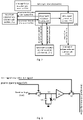
- Fig. 1 is a schematic view showing an image sensor 100 according to one embodiment of the present disclosure.
- the image sensor 100 is applied to a scenario where an object moving at a high speed is to be detected, so as to output an event data stream associated with a motion event.
- the image sensor 100 is coupled to an external image processor (not shown), and outputs an image representing time information to the external image processor for the subsequent calculation and application.
- the image processor is used to implement some machine vision algorithms, e.g., object detection and object tracking, which will not be particularly defined herein.
- the image sensor 100 includes a pixel collection circuit array 110, a global control unit 120 and a reading unit 130.
- the pixel collection circuit array 110 consists of a plurality of pixel collection circuits 200 arranged evenly in both a row direction and a column direction.
- Fig. 1 shows a 3 ⁇ 3 pixel collection circuit array.
- the global control unit 120 is coupled to the pixel collection circuit array 110, and configured to control an initial operating state of the pixel collection circuit array 110. Generally, the global control unit 120 takes charge of resetting the entire pixel collection circuit array 110 when the image sensor 100 is powered on, so as to enable each pixel collection circuit 112 to be maintained in a stable initial state. Then, the pixel collection circuit array 110 starts to operate normally.
- the reading unit 130 is coupled to the pixel collection circuit array 110.
- the reading unit 130 is configured to manage events generated by the pixel collection circuit array 110, and scan the time signal generated by the pixel collection circuit array 110 to generate an image associated with time information about the pixel collection circuit array 110.
- a position of a pixel in the image indicates a row address and a column address of the pixel collection circuit, and a size of the pixel is a size of the time signal generated by the pixel collection circuit.
- the image is called as a time surface frame (TimeSurface) which reflects the distribution of dynamic information in a field of view in time and space over a small time period.
- the above two functions of the reading unit 130 are independent of each other.
- the reading unit 130 includes three sub-units, i.e., a row selection module 132, a column selection module 134 and a reading control module 136.
- the row selection module 132 is configured to manage the pixel collection circuit array 110 in the row direction
- the column selection module 134 is configured to manage the pixel collection circuit array 110 in the column direction
- the reading control module 136 is configured to coordinate the row selection module 132 and the column selection module 134.
- the pixel collection circuit 200 includes not only a movement detection module 210 but also a time signal generation module 220, as shown in Fig. 2 .
- the movement detection module 210 is configured to detect dynamic information in the field of view.
- the time signal generation module 220 is configured to generate a local time signal, and the time signal is used to represent time information about a time point at which the pixel collection circuit is triggered.
- the movement detection module 210 is configured to detect in real time a change in a light intensity in the field of view, and generate a pixel triggering signal when the change in the light intensity exceeds a predetermined threshold so as to indicate the pixel collection circuit to be in a triggered state.
- the time signal generation module 220 of the pixel collection circuit 200 generates a local time signal, and usually the time signal is a voltage signal.
- the time signal indicates an instantaneous voltage pulse when the pixel collection circuit 200 enters the triggered state, and subsequently an amplitude of the time signal is attenuated over time. Hence, through obtaining the amplitude of the time signal at a certain time point, it is able to determine whether and when an event is detected by the pixel collection circuit 200.
- the row selection module 132 includes a movement detection row selection sub-module 1322 and a time signal row selection sub-module 1324
- the column selection module 132 includes a movement detection column selection sub-module 1342 and a time signal column selection sub-module 1344, as shown in Fig. 1 .
- the reading unit 130 For each pixel collection circuit 200 in the pixel collection circuit array 110, the reading unit 130 is coupled thereto via a corresponding bus, so as to manage the event and scan the time signal. In addition, for the reading unit 130, the managing of the event is independent of the scanning of the time signal. The two procedures will be described hereinafter in more details in conjunction with Fig. 2 .
- the movement detection row selection sub-module 1322 is coupled to the movement detection module 210 of the pixel collection circuit 200 via a movement detection row request line and a movement detection row selection line
- the movement detection column selection sub-module 1342 is coupled to the movement detection unit 210 of the pixel collection circuit 200 via a movement detection column request line and a movement detection column selection line.
- the movement detection module 210 of the pixel collection circuit 200 may set a corresponding movement detection row request line as active.
- the movement detection row selection sub-module 1322 may manage all the movement detection row request lines for the pixel collection circuit array 110, and response to a received row request signal.
- the movement detection row selection module 1322 sets a corresponding movement row selection lien as active, so as to respond to active row request signal.
- a response has been obtained with respect to a row request signal from the pixel collection circuits in a certain row, column request signals from the pixel collection circuits in the row are active.
- the movement detection column selection sub-module 1342 respond to these column request signals.
- the movement detection column selection sub-module 1342 manages all the column request signals in the column direction, and set a corresponding movement detection column selection line as active to release the corresponding pixel collection circuit from being in the triggered state, so that the pixel collection circuit may respond to the change in the light intensity again.
- the reading control module 136 notifies the movement detection row selection sub-module 1322 to perform a row switching operation.
- the movement detection row selection sub-module 1322 cancels a movement detection row selection signal for a current row, and selects a next row, until all the pixel collection circuits in the pixel collection circuit array 110 have been scanned.
- the time signal row selection sub-module 1324 is coupled to the time signal generation module 220 of the pixel collection circuit 200 via a time signal row selection line
- the time signal column selection sub-module 1344 is coupled to the time signal generation module 220 of the pixel collection circuit 200 via a time signal column output line.
- the time signal row selection sub-module 1324 sets the time signal row selection lines as active progressively (e.g., a first time signal row selection line is set as active at first).
- the time signal row selection line coupled to the pixel collection circuit 200 is active, the pixel collection circuit 200 outputs the time signal to the time signal column output line.
- the time signal column selection sub-module 1344 scans the time signals from the pixel collection circuit 200 progressively via the time signal column output line.
- the reading control module 136 notifies the time signal row selection sub-module 1324 to perform a row switching operation.
- the time signal row selection sub-module 1324 cancels the time signal row selection signal for the current row, and selects a next row, until the time signals from the pixel collection circuits 200 in a last row have been read.
- a time surface frame is formed.
- the reading control module 136 cancels the time signal row selection signal for the last row, and sets the time signal row selection signal for the first row as active for the subsequent reading of a next time surface frame.
- the image sensor 100 Based on the above-mentioned reading mechanism, the image sensor 100 outputs a synchronous time surface frame.
- the time surface frame includes time-space information about an object moving the field of view, and it may be directly used by the back-end machine vision algorithm as a training sample for implementing such tasks as object identification and object tracking.
- the movement detection row selection sub-module 1322 and the movement detection column selection sub-module 1342 may be implemented in the form of a selection scanning circuit or a decision circuit
- the time signal row selection sub-module 1324 and the time signal column selection sub-module 1344 may be implemented in the form of a full scanning circuit.
- the above circuits are known in the art and thus will not be particularly defined herein.
- the movement detection module 210 includes a photoelectric detection sub-module 212, a triggering generation sub-module 214 and a reading interface sub-module 216 coupled to each other.
- the photoelectric detection sub-module 212 is configured to monitor in real time a light signal, and output a corresponding electric signal.
- a first input end of the triggering generation sub-module 214 is coupled to the photoelectric detection sub-module 212, a first output end thereof is coupled to the reading interface sub-module 216, and a second output end thereof is coupled to the time signal regeneration module 220.
- the triggering generation sub-module 214 When the electric signal meets a predetermined triggering condition, the triggering generation sub-module 214 generates a triggering generation signal and outputs it to the reading interface sub-module 216 and the time signal generation module 220.
- the reading interface sub-module 216 is coupled to the triggering generation sub-module 214, so as to communicate with the reading unit 130.
- the movement detection module 210 is known in the conventional dynamic vision sensor, and thus will not be particularly defined herein.
- the time signal indicates an instantaneous voltage pulse when the pixel collection circuit 200 enters the triggered state, and subsequently the time signal is attenuated over time.
- the time signal may be attenuated exponentially or linearly, which will not be particularly defined herein.
- Figs. 3 and 5 show two time signal generation modules 220, where for the time signal generation module 220 in Fig. 3 , the time signal is attenuated exponentially, while for the time signal generation module 220 in Fig. 5 , the time signal is attenuated linearly.
- the time signal generation module 220 includes a first switch K1, a first capacitor C1, a first resistor R1, a first buffer B1 and a second switch K2.
- a first end of the first switch K1 is coupled to a fixed voltage VA, and a second end thereof is coupled to a first end of the first buffer B1.
- the first capacitor C1 and the first resistor R1 are connected in parallel, one end of each of the first capacitor C1 and the first resistor R1 is grounded, and the other end is coupled to the second end of the first switch K1 and the first end of the first buffer B1.
- a second end of the first buffer B1 is coupled to a first end of the second switch K2, and a second end of the second switch K2 is coupled to a time signal column output line.
- the first switch K1 is controlled by a pixel triggering signal from the movement detection module 210, and when the pixel triggering signal is active, the first switch K1 is turned on.
- the second switch K2 is controlled by a time signal row selection signal from the reading unit 130, and when the time signal row selection signal is active, the second switch K2 is turned on.
- the first resistor R1 is an adjustable resistor. An attenuation rate of the time signal is determined in accordance with a time constant consisting of the first capacitor C1 and the first resistor R1.
- Figs. 4A to 4D show waveforms of the time signal generated by the time signal generation module 220 in Fig. 3 .
- Fig. 4A shows the time signal generated when the pixel collection circuit 200 is triggered once
- Fig. 4B shows the time signal generated when the pixel collection circuit 200 is triggered many times (e.g., when the pixel collection circuit 200 is triggered twice consecutively).
- an x-axis represents time t
- a y-axis represents the pixel triggering signal VT
- Figs. 4C and 4D show the waveforms corresponding to the time signals in Figs. 4A and 4B respectively.
- an x-axis represents time t
- a y-axis represents a voltage V1 of the time signal.
- the pixel collection circuit when the pixel collection circuit is not triggered (t ⁇ t1), the pixel triggering signal VT is at a low level, so the first switch K1 is turned off, and V1 is discharged to 0V through the first resistor R1.
- the pixel collection circuit 200 is triggered, and the pixel triggering signal VT is a very short pulse signal.
- the first switch K1 is turned on, and the first capacitor C1 is forcibly charged to the fixed voltage VA, i.e., V1 is instantaneously pulled up to VA at t1.
- the pixel triggering signal is inactive, the first switch K1 is turned off again, and the first capacitor C1 is slowly discharged through the first resistor R1, i.e., V1 is attenuated exponentially.
- V1 is attenuated to 0V.
- the pixel collection circuit 200 is triggered at t1 and t2, and there is a short time period between t1 and t2.
- the pixel triggering signal VT is a narrow pulse, so the first switch K1 is turned on and the time signal V1 is forcibly pulled up to the fixed voltage VA. Then, the first switch K1 is turned off, and V1 is attenuated exponentially.
- the pixel collection circuit 200 is triggered again at t2, the pixel triggering signal VT is a narrow pulse again, and the time signal V1 is pulled up to VA again. Then, the first switch K1 is turned off, and V1 is attenuated exponentially.
- the time signal row selection signal is active, so the second switch K2 is turned on, V1 is delivered to the time signal column output line via the first buffer B1, and the column selection module 134 obtains and outputs V1.
- an instantaneous amplitude of the time signal at a certain time point may represent time information about a time period between a time point where the pixel collection circuit is triggered and a current time point.
- the attenuation rate of the time signal is determined in accordance with the time constant consisting of the first capacitor C1 and the first resistor R1.
- the first resistor R1 is an adjustable resistor. A resistance of the first resistor R1 may be changed according to the practical need, so as to adjust the attenuation rate of the time signal.
- Fig. 5 shows the time signal generation module 220 where the time signal is attenuated linearly.
- the first resistor R1 is replaced with a constant current source I.
- a third switch K3 is turned off, a second capacitor C2 is discharged through the constant current source I, so that the time signal V2 is attenuated linearly over time.
- the time signal generation module 220 includes the third switch K3, the second capacitor C2, the constant current source I, a second buffer B2 and a fourth switch K4.
- a first end of the third switch K3 is coupled to a fixed voltage VA, and a second end thereof is coupled to a first end of the second buffer B2.
- the second capacitor C2 and the constant current source I are connected in parallel, one end of each of the second capacitor C2 and the constant current source I is grounded, and the other end is coupled to a second end of the third switch K3 and the first end of the second buffer B2.
- a second end of the second buffer B2 is coupled to a first end of the fourth switch K4, and a second end of the fourth switch K4 is coupled to a time signal column output line.
- the third switch K3 si controlled by the pixel triggering signal from the movement detection module 210, and when the pixel triggering signal is active, the third switch K3 is turned on.
- the fourth switch K4 is controlled by the time signal row selection signal from the reading unit 130, and when the time signal row selection signal is active, the fourth switch K4 is turned on.
- the attenuation rate of the time signal is determined in accordance with the second capacitor C2 and the constant current source I.
- Figs. 6A to 6D show the waveforms of the time signal generated by the time signal generation module 220 in Fig. 5 .
- Fig. 6A shows the time signal generated when the pixel collection circuit 200 is triggered once
- Fig. 6B shows the time signal generated when the pixel collection circuit 200 is triggered many times (e.g., when the pixel collection circuit 200 is triggered twice consecutively).
- an x-axis represents time t
- a y-axis represents the pixel triggering signal VT.
- Figs. 6C and 6D show the waveforms corresponding to the time signals in Figs. 6A and 6B respectively.
- an x-axis represents time t
- a y-axis represents a voltage V2 of the time signal.
- the pixel collection circuit when the pixel collection circuit is not triggered (t ⁇ t1), the pixel triggering signal VT is at a low level, so the third switch K3 is turned off, and V2 is discharged to 0V through the constant current source I.
- the pixel collection circuit 200 is triggered, and the pixel triggering signal VT is a very short pulse signal.
- the third switch K3 is turned on, and the second capacitor C2 is forcibly charged to the fixed voltage VA, i.e., V2 is instantaneously pulled up to VA at t1.
- the pixel triggering signal is inactive, the third switch K3 is turned off again, and the second capacitor C2 is slowly discharged through the constant current source I, i.e., V2 is attenuated linearly.
- V2 is attenuated to 0V.
- the pixel collection circuit 200 is triggered at t1 and t2, and there is a short time period between t1 and t2.
- the pixel triggering signal VT is a narrow pulse
- the third switch K3 is turned on and the time signal V2 is forcibly pulled up to the fixed voltage VA.
- the third switch K3 is turned off, and V2 is attenuated linearly.
- the pixel collection circuit 200 is triggered again at t2, the pixel triggering signal VT is a narrow pulse again, and the time signal V2 is pulled up to VA again.
- the third switch K3 is turned off, and V2 is attenuated linearly.
- the time signal row selection signal is active, so the fourth switch K4 is turned on, V2 is delivered to the time signal column output line via the second buffer B2, and the column selection module 134 obtains and outputs V2.
- the time information represented by the instantaneous amplitude of the time signal may be understood in a better manner through the waveform of the time signal generated when the pixel collection circuit is triggered once in Fig. 6C .
- a linear discharging time period (t1 to t3) is 20ms, i.e., VA is completely discharged to 0V after 20ms.
- an instantaneous voltage amplitude is normalized in accordance with an amplitude of VA, i.e., the instantaneous voltage amplitude is a normalized amplitude within a range from 0 to 1. As shown in Fig.
- the normalized amplitude When the normalized amplitude is 0, it means that the pixel collection circuit 200 has been triggered for more than 20ms at the reading time point, or the pixel collection circuit 200 has not been triggered yet.
- the pixel collection circuit 200 which was triggered a long time ago may be considered that as non-triggered pixel collection circuit, because the time surface frame merely focuses on the movement generated at the current time point and a time point immediately before the current time point, rather than the movement generated a long time ago. It should be appreciated that, the value of the linear discharging time and the value of the normalized amplitude are for illustrative purposes only, and the present disclosure is not limited thereto.
- the attenuation rate of the time signal is determined by the second capacitor C2 and the constant current source I.
- Figs. 3 and 5 merely show the exemplary time signal generation modules 220 where the time signals are attenuated exponentially and linearly respectively, and the time signal generation module 220 where the time signal is attenuated in the other forms may be implemented in different ways, which will not be particularly defined herein.
- Fig. 7 shows a field of view according to one embodiment of the present disclosure
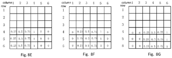
- Figs. 8A to 8G show the time surface fame in the scenario in Fig. 7 .
- the pixel collection circuit array 110 of the image sensor 100 includes pixel collection circuits 200 in 6 rows and 6 columns.
- the field of view corresponding to the pixel collection circuit array 110 is a white background.
- a black object A (filled with grids in Fig. 7 ) enters the field of view from the bottom left and moves horizontally to a rightmost side of the field of view.
- a movement trajectory of the object A covers all the pixel collection circuits in a fourth row to a sixth row.
- the object A is located at a left boundary of the field of view at a time point 0, and its movement speed is 5ms per pixel collection circuit.
- the pixel collection circuits triggered by the object A are filled with "/", and a corresponding triggering time point is shown.
- a pixel collection circuit in a fifth row and a fourth column is triggered at 20ms.
- the pixel collection circuits not filled with "/" are non-triggered pixel collection circuits.
- the time signal row selection sub-module 1324 and the time signal column selection sub-module 1344 need to scan the entire pixel collection circuit array 110 progressively under the control of the reading unit 130, so as to obtain the time signal generated by the time signal generation module 220 of each pixel collection circuit 200.
- the time signal generation module 220 in Fig. 5 is adopted.
- a discharging time is set as 20ms, and an output amplitude is normalized, so as to describe the output of the time information (i.e., the time surface frame) about the pixel collection circuit.
- a triggering time point of a pixel collection circuit 200 When a triggering time point of a pixel collection circuit 200 is closer to a reading time point of a current time surface frame, a corresponding normalized amplitude is closer to 1, and in contrast, the corresponding normalized amplitude is closer to 0.
- the image sensor 100 When one time surface frame is obtained by the reading unit 130 every 5ms, the image sensor 100 outputs six time surface frames from 5ms to 30ms, as shown in Figs. 8B to 8G .
- the time surface frames are marks as time surface frame 1, time surface frame 2, time surface frame 3, ..., and time surface frame 6 outputted at time points as 5ms, 10ms, 15ms, 20ms, 25ms and 30ms respectively.
- Fig. 8B i.e., the time surface frame 1
- its reading time point is 5ms.
- the pixel collection circuits in a first column and in fourth to sixth rows are triggered at the time point 5ms.
- the normalized amplitudes of these pixel collection circuits are 1, and the normalized amplitudes of the other pixel collection circuits are 0.
- Fig. 8C For Fig. 8C (i.e., the time surface frame 2), its reading time point is 10ms.
- the pixel collection circuits in a first column and in fourth to sixth rows are triggered at the time point 5ms, so the normalized amplitudes of these pixel collection circuits are 0.75 (1-(10ms-5ms)/20ms).
- the pixel collection circuits in a second column and in fourth to sixth rows are triggered at the time point 10ms, so the normalized amplitudes of these pixel collection circuits are 1.
- the normalized amplitudes of the other pixel collection circuits are 0.
- Fig. 8D For Fig. 8D (i.e., the time surface frame 3), its reading time point is 15ms.
- the pixel collection circuits in a first column and in fourth to sixth rows are triggered at the time point 5ms, so the normalized amplitudes of these pixel collection circuits are 0.5 (1-(15ms-5ms)/20ms).
- the pixel collection circuits in a second column and in fourth to sixth rows are triggered at the time point 10ms, so the normalized amplitudes of these pixel collection circuits are 0.75 (1-(15ms-10ms)/20ms).
- the pixel collection circuits in a third column and in fourth to sixth rows are triggered at the time point 15ms, so the normalized amplitudes of these pixel collection circuits is 1.
- the normalized amplitudes of the other pixel collection circuits are 0.
- Fig. 8E For Fig. 8E (i.e., the time surface frame 4), its reading time point is 20ms.
- the pixel collection circuits in a first column and in fourth to sixth rows are triggered at the time point 5ms, so the normalized amplitudes of these pixel collection circuits are 0.25 (1-(20ms-5ms)/20ms).
- the pixel collection circuits in a second column and in fourth to sixth rows are triggered at the time point 10ms, so the normalized amplitudes of these pixel collection circuits are 0.5 (1-(20ms-10ms)/20ms).
- the pixel collection circuits in a third column and in fourth to sixth rows are triggered at the time point 15ms, so the normalized amplitudes of these pixel collection circuits are 0.75 (1-(20ms-15ms)/20ms).
- the pixel collection circuits in a fourth column and in fourth to sixth rows are triggered at the time point 20ms, so the normalized amplitudes of these pixel collection circuits are 1.
- the normalized amplitudes of the other pixel collection circuits are 0.
- Fig. 8F For Fig. 8F (i.e., the time surface frame 5), its reading time point is 25ms.
- the pixel collection circuits in a first column and in fourth to sixth rows are triggered at the time point 5ms, so the normalized amplitudes of these pixel collection circuits are 0 (1-(25ms-5ms)/20ms).
- the pixel collection circuits in a second column and in fourth to sixth rows are triggered at the time point 10ms, so the normalized amplitudes of these pixel collection circuits are 0.25 (1-(25ms-10ms)/20ms).
- the pixel collection circuits in a third column and in fourth to sixth rows are triggered at the time point 15ms, so the normalized amplitudes of these pixel collection circuits are 0.5 (1-(25ms-15ms)/20ms).
- the pixel collection circuits in a fourth column and in fourth to sixth rows are triggered at the time point 20ms, so the normalized amplitudes of these pixel collection circuits are 0.75 (1-(25ms-20ms)/20ms).
- the pixel collection circuits in a fifth column and in fourth to sixth rows are triggered at the time point 25ms, so the normalized amplitudes of these pixel collection circuits is 1.
- the normalized amplitudes of the other pixel collection circuits are 0.
- Fig. 8G For Fig. 8G (i.e., the time surface frame 6), its reading time point is 30ms.
- the pixel collection circuits in a first column and in fourth to sixth rows are triggered at the time point 5ms, so the normalized amplitudes of these pixel collection circuits is 0 (a time period between the current reading time point and a time point at which these pixel collection circuits were previously triggered is greater than the discharging time 20ms).
- the pixel collection circuits in a first column and in fourth to sixth rows are triggered at the time point 10ms, so the normalized amplitudes of these pixel collection circuits are 0 (1-(30ms-10ms)/20ms).
- the pixel collection circuits in a third column and in fourth to sixth rows are triggered at the time point 15ms, so the normalized amplitudes of these pixel collection circuits are 0.25 (1-(30ms-15ms)/20ms).
- the pixel collection circuits in a fourth column and in fourth to sixth rows are triggered at the time point 20ms, so the normalized amplitudes of these pixel collection circuits are 0.5 (1-(30ms-20ms)/20ms).
- the pixel collection circuits in a fifth column and in fourth to sixth rows are triggered at the time point 25ms, so the normalized amplitudes of these pixel collection circuits are 0.75 (1-(30ms-25ms)/20ms).
- the pixel collection circuits in a sixth column and in fourth to sixth rows are triggered at the time point 30ms, so the normalized amplitudes of these pixel collection circuits is 1.
- the normalized amplitudes of the other pixel collection circuits are 0.25 (1-(
- the pixel collection circuit 200 is provided with the additional time signal generation module 220 for generating a local time signal.
- the time signal is a voltage signal, and it is an instantaneous voltage pulse when an event has been detected by the pixel collection circuit 200 and then attenuated gradually to indicate the elapse of time.
- the peripheral reading unit 130 is provided with the additional time signal row selection sub-module 1324 and the additional time signal column selection sub-module 1344, so as to regularly scan the time signals outputted by the time signal generation modules 220 of all the pixel collection circuits 200, thereby to generate and output the time surface frame.
- the image sensor 100 may asynchronously detect the dynamic information like the conventional dynamic vision sensor, and directly output the time surface frame representing the time information about the pixel collection circuit to a back-end machine vision algorithm.
- the time surface frame may be used by the back-end machine vision algorithm as a train sample, and use to implement such tasks as object identification and tracking. As a result, it is able to reduce the overhead of storage and computation for data conversion at a back end of an image processing system, thereby to improve the efficiency of the image processing system.
- modules, units or components in the above examples may be arranged in the device described in the embodiments, or in one or more devices different from the device.
- the modules may be combined into one module, or each module may be divided into a plurality of submodules.
- the modules may be modified adaptively and arranged in one or more devices different from that mentioned hereinabove.
- the modules, units or components may be combined into one module, unit or component, or each module, unit or component may be divided into a plurality of submodules, subunits or subcomponents.
- all the features, processes or units involved in the specification may be combined in any form. Unless otherwise defined, each feature in the specification (including the appended claims, abstract and drawings) may be replaced with a same, equivalent or similar feature.
- the embodiments have been described as a combination of methods or method elements capable of being implemented by a processor of a computer system or any other device.
- the processor including necessary instructions for implementing the methods or the method elements may be used to form a device for implementing the methods or the method elements.
- the device is used to achieve functions of the elements.
Landscapes
- Engineering & Computer Science (AREA)
- Multimedia (AREA)
- Signal Processing (AREA)
- Transforming Light Signals Into Electric Signals (AREA)
Applications Claiming Priority (2)
| Application Number | Priority Date | Filing Date | Title |
|---|---|---|---|
| CN201911203365.3A CN111107287B (zh) | 2019-11-29 | 2019-11-29 | 一种像素采集电路及图像传感器 |
| PCT/CN2020/078229 WO2021103341A1 (fr) | 2019-11-29 | 2020-03-06 | Circuit de captage de pixels et capteur d'image |
Publications (3)
| Publication Number | Publication Date |
|---|---|
| EP4068760A1 true EP4068760A1 (fr) | 2022-10-05 |
| EP4068760A4 EP4068760A4 (fr) | 2023-01-04 |
| EP4068760B1 EP4068760B1 (fr) | 2025-07-16 |
Family
ID=70421369
Family Applications (1)
| Application Number | Title | Priority Date | Filing Date |
|---|---|---|---|
| EP20892079.3A Active EP4068760B1 (fr) | 2019-11-29 | 2020-03-06 | Capteur d'image |
Country Status (5)
| Country | Link |
|---|---|
| US (1) | US12015861B2 (fr) |
| EP (1) | EP4068760B1 (fr) |
| JP (1) | JP7428307B2 (fr) |
| CN (1) | CN111107287B (fr) |
| WO (1) | WO2021103341A1 (fr) |
Families Citing this family (2)
| Publication number | Priority date | Publication date | Assignee | Title |
|---|---|---|---|---|
| US11694304B2 (en) * | 2019-11-26 | 2023-07-04 | Samsung Electronics Co., Ltd. | Jointly learning visual motion and confidence from local patches in event cameras |
| WO2022047651A1 (fr) * | 2020-09-02 | 2022-03-10 | 华为技术有限公司 | Puce de capteur de vision et son procédé de fonctionnement, et dispositif électronique |
Family Cites Families (14)
| Publication number | Priority date | Publication date | Assignee | Title |
|---|---|---|---|---|
| AT504582B1 (de) | 2006-11-23 | 2008-12-15 | Arc Austrian Res Centers Gmbh | Verfahren zur generierung eines bildes in elektronischer form, bildelement für einen bildsensor zur generierung eines bildes sowie bildsensor |
| US8687060B1 (en) * | 2009-12-28 | 2014-04-01 | Cognex Corporation | System and method for providing distance-based pulses relative to motion of a surface scanned by a vision system |
| KR102022970B1 (ko) * | 2013-04-30 | 2019-11-04 | 삼성전자주식회사 | 시각 센서에 기반하여 공간 정보를 감지하는 장치 및 방법 |
| KR102136055B1 (ko) | 2014-01-08 | 2020-07-21 | 삼성전자 주식회사 | 오픈-루프 증폭기를 포함하는 비전 센서 칩, 이의 동작 방법, 및 이를 포함하는 데이터 처리 시스템 |
| CN106162000B (zh) * | 2016-07-08 | 2019-03-15 | 上海芯仑光电科技有限公司 | 像素采集电路、图像传感器及图像采集系统 |
| JP7074954B2 (ja) * | 2016-12-30 | 2022-05-25 | ソニー アドバンスト ビジュアル センシング アーゲー | 動的ビジョンセンサアーキテクチャ |
| CN108632546B (zh) * | 2017-03-17 | 2021-06-04 | 豪威芯仑传感器(上海)有限公司 | 像素采集电路、光流传感器及图像采集系统 |
| US10348994B2 (en) * | 2017-04-06 | 2019-07-09 | Samsung Electronics Co., Ltd. | Intensity image acquisition from dynamic vision sensors |
| CN108449557B (zh) | 2018-03-23 | 2019-02-15 | 上海芯仑光电科技有限公司 | 像素采集电路、光流传感器和光流及图像信息采集系统 |
| CN108827461B (zh) * | 2018-04-25 | 2019-05-03 | 上海芯仑光电科技有限公司 | 像素采集电路及光流传感器 |
| WO2019211317A1 (fr) | 2018-04-30 | 2019-11-07 | Prophesee | Systèmes et procédés pour une détection d'image asynchrone basée sur le temps |
| CN109377516B (zh) * | 2018-11-01 | 2020-09-29 | 清华大学 | 一种使用动态视觉数据的光流计算方法 |
| CN109842767B (zh) * | 2019-01-09 | 2020-07-14 | 上海芯仑光电科技有限公司 | 一种防闪光电路组件及图像传感器 |
| CN109842768B (zh) * | 2019-01-29 | 2020-05-15 | 上海芯仑光电科技有限公司 | 一种像素采集电路及图像传感器 |
-
2019
- 2019-11-29 CN CN201911203365.3A patent/CN111107287B/zh active Active
-
2020
- 2020-03-06 EP EP20892079.3A patent/EP4068760B1/fr active Active
- 2020-03-06 JP JP2022525427A patent/JP7428307B2/ja active Active
- 2020-03-06 WO PCT/CN2020/078229 patent/WO2021103341A1/fr not_active Ceased
-
2022
- 2022-04-28 US US17/731,305 patent/US12015861B2/en active Active
Also Published As
| Publication number | Publication date |
|---|---|
| EP4068760A4 (fr) | 2023-01-04 |
| JP7428307B2 (ja) | 2024-02-06 |
| CN111107287A (zh) | 2020-05-05 |
| JP2023501237A (ja) | 2023-01-18 |
| US20220256109A1 (en) | 2022-08-11 |
| EP4068760B1 (fr) | 2025-07-16 |
| CN111107287B (zh) | 2021-06-04 |
| WO2021103341A1 (fr) | 2021-06-03 |
| US12015861B2 (en) | 2024-06-18 |
Similar Documents
| Publication | Publication Date | Title |
|---|---|---|
| US12022211B1 (en) | Pixel collection circuit, optical flow sensor, and optical flow and image information collection system | |
| JP7383616B2 (ja) | イベントベースセンサから信号を出力するための方法、およびそのような方法を使用するイベントベースセンサ | |
| US12015861B2 (en) | Pixel collection circuit and image sensor | |
| US10181194B2 (en) | Pixel acquisition circuit, optical flow sensor, and image acquisition system | |
| EP3226138B1 (fr) | Système et dispositif de test de puce d'acquisition de données et procédé de commande pour ceux-ci | |
| US11095821B2 (en) | Focus control apparatus and method generating and utilizing distance histogram for selection and setting of focus area | |
| EP3913907B1 (fr) | Circuit d'acquisition de pixels et capteur d'image | |
| EP3989535B1 (fr) | Dispositif de conversion photoélectrique, procédé de commande de dispositif de conversion photoélectrique et appareil de traitement d'informations | |
| EP4024849B1 (fr) | Capteur d'image et système d'acquisition d'image | |
| US11119603B2 (en) | Touch control chip, electronic device having the same and touch detection method therefor | |
| WO2014184436A1 (fr) | Procédé et appareil de reconnaissance d'utilisateur en direct | |
| US11164019B1 (en) | Object detection for event cameras | |
| EP3358450A1 (fr) | Panneau tactile, dispositif terminal et procédé de détection d'un point touché | |
| JP2024516801A (ja) | 画像センサ及び画像処理システム | |
| US20210333974A1 (en) | Touch detection method and touch display device | |
| CN113610022A (zh) | 指纹识别电路、显示面板及其控制方法 | |
| CN110809113A (zh) | 一种基于fpga的红外成像自动聚焦系统 | |
| US11683605B2 (en) | Image sensor chip and sensing method thereof | |
| CN109584278B (zh) | 一种目标识别装置及方法 | |
| CN113747090A (zh) | 一种像素采集电路及图像传感器 | |
| KR101473189B1 (ko) | 지문 검출 장치 및 이의 메모리 제어 방법 | |
| KR20100069345A (ko) | 접촉 감지 기능이 있는 표시 장치 및 접촉 판단 방법 | |
| CN112860077A (zh) | 显示面板的信号读取方法和装置 | |
| CN117223037A (zh) | 瞳孔信息采集电路及方法、显示装置 | |
| JPS5875277A (ja) | パタ−ン認識装置 |
Legal Events
| Date | Code | Title | Description |
|---|---|---|---|
| STAA | Information on the status of an ep patent application or granted ep patent |
Free format text: STATUS: THE INTERNATIONAL PUBLICATION HAS BEEN MADE |
|
| PUAI | Public reference made under article 153(3) epc to a published international application that has entered the european phase |
Free format text: ORIGINAL CODE: 0009012 |
|
| STAA | Information on the status of an ep patent application or granted ep patent |
Free format text: STATUS: REQUEST FOR EXAMINATION WAS MADE |
|
| 17P | Request for examination filed |
Effective date: 20220513 |
|
| AK | Designated contracting states |
Kind code of ref document: A1 Designated state(s): AL AT BE BG CH CY CZ DE DK EE ES FI FR GB GR HR HU IE IS IT LI LT LU LV MC MK MT NL NO PL PT RO RS SE SI SK SM TR |
|
| REG | Reference to a national code |
Free format text: PREVIOUS MAIN CLASS: H04N0005345000 Ipc: H04N0005374500 Ref country code: DE Ref legal event code: R079 Ref document number: 602020054793 Country of ref document: DE Free format text: PREVIOUS MAIN CLASS: H04N0005345000 Ipc: H04N0005374500 |
|
| A4 | Supplementary search report drawn up and despatched |
Effective date: 20221206 |
|
| RIC1 | Information provided on ipc code assigned before grant |
Ipc: H04N 5/3745 20110101AFI20221130BHEP |
|
| DAV | Request for validation of the european patent (deleted) | ||
| DAX | Request for extension of the european patent (deleted) | ||
| STAA | Information on the status of an ep patent application or granted ep patent |
Free format text: STATUS: EXAMINATION IS IN PROGRESS |
|
| 17Q | First examination report despatched |
Effective date: 20240313 |
|
| REG | Reference to a national code |
Ref country code: DE Ref legal event code: R079 Free format text: PREVIOUS MAIN CLASS: H04N0005374500 Ipc: H04N0025470000 Ref country code: DE Ref legal event code: R079 Ref document number: 602020054793 Country of ref document: DE Free format text: PREVIOUS MAIN CLASS: H04N0005374500 Ipc: H04N0025470000 |
|
| GRAP | Despatch of communication of intention to grant a patent |
Free format text: ORIGINAL CODE: EPIDOSNIGR1 |
|
| STAA | Information on the status of an ep patent application or granted ep patent |
Free format text: STATUS: GRANT OF PATENT IS INTENDED |
|
| RIC1 | Information provided on ipc code assigned before grant |
Ipc: H04N 25/78 20230101ALI20250203BHEP Ipc: H04N 25/76 20230101ALI20250203BHEP Ipc: H04N 25/707 20230101ALI20250203BHEP Ipc: H04N 25/772 20230101ALI20250203BHEP Ipc: H04N 25/47 20230101AFI20250203BHEP |
|
| INTG | Intention to grant announced |
Effective date: 20250212 |
|
| GRAS | Grant fee paid |
Free format text: ORIGINAL CODE: EPIDOSNIGR3 |
|
| GRAA | (expected) grant |
Free format text: ORIGINAL CODE: 0009210 |
|
| STAA | Information on the status of an ep patent application or granted ep patent |
Free format text: STATUS: THE PATENT HAS BEEN GRANTED |
|
| AK | Designated contracting states |
Kind code of ref document: B1 Designated state(s): AL AT BE BG CH CY CZ DE DK EE ES FI FR GB GR HR HU IE IS IT LI LT LU LV MC MK MT NL NO PL PT RO RS SE SI SK SM TR |
|
| REG | Reference to a national code |
Ref country code: GB Ref legal event code: FG4D |
|
| REG | Reference to a national code |
Ref country code: CH Ref legal event code: EP |
|
| REG | Reference to a national code |
Ref country code: DE Ref legal event code: R096 Ref document number: 602020054793 Country of ref document: DE |
|
| REG | Reference to a national code |
Ref country code: IE Ref legal event code: FG4D |
|
| REG | Reference to a national code |
Ref country code: NL Ref legal event code: MP Effective date: 20250716 |
|
| PG25 | Lapsed in a contracting state [announced via postgrant information from national office to epo] |
Ref country code: PT Free format text: LAPSE BECAUSE OF FAILURE TO SUBMIT A TRANSLATION OF THE DESCRIPTION OR TO PAY THE FEE WITHIN THE PRESCRIBED TIME-LIMIT Effective date: 20251117 |
|
| PG25 | Lapsed in a contracting state [announced via postgrant information from national office to epo] |
Ref country code: NL Free format text: LAPSE BECAUSE OF FAILURE TO SUBMIT A TRANSLATION OF THE DESCRIPTION OR TO PAY THE FEE WITHIN THE PRESCRIBED TIME-LIMIT Effective date: 20250716 |
|
| REG | Reference to a national code |
Ref country code: AT Ref legal event code: MK05 Ref document number: 1815207 Country of ref document: AT Kind code of ref document: T Effective date: 20250716 |
|
| PG25 | Lapsed in a contracting state [announced via postgrant information from national office to epo] |
Ref country code: IS Free format text: LAPSE BECAUSE OF FAILURE TO SUBMIT A TRANSLATION OF THE DESCRIPTION OR TO PAY THE FEE WITHIN THE PRESCRIBED TIME-LIMIT Effective date: 20251116 |
|
| PG25 | Lapsed in a contracting state [announced via postgrant information from national office to epo] |
Ref country code: NO Free format text: LAPSE BECAUSE OF FAILURE TO SUBMIT A TRANSLATION OF THE DESCRIPTION OR TO PAY THE FEE WITHIN THE PRESCRIBED TIME-LIMIT Effective date: 20251016 |
|
| REG | Reference to a national code |
Ref country code: LT Ref legal event code: MG9D |
|
| PG25 | Lapsed in a contracting state [announced via postgrant information from national office to epo] |
Ref country code: AT Free format text: LAPSE BECAUSE OF FAILURE TO SUBMIT A TRANSLATION OF THE DESCRIPTION OR TO PAY THE FEE WITHIN THE PRESCRIBED TIME-LIMIT Effective date: 20250716 |
|
| PG25 | Lapsed in a contracting state [announced via postgrant information from national office to epo] |
Ref country code: FI Free format text: LAPSE BECAUSE OF FAILURE TO SUBMIT A TRANSLATION OF THE DESCRIPTION OR TO PAY THE FEE WITHIN THE PRESCRIBED TIME-LIMIT Effective date: 20250716 |
|
| PG25 | Lapsed in a contracting state [announced via postgrant information from national office to epo] |
Ref country code: HR Free format text: LAPSE BECAUSE OF FAILURE TO SUBMIT A TRANSLATION OF THE DESCRIPTION OR TO PAY THE FEE WITHIN THE PRESCRIBED TIME-LIMIT Effective date: 20250716 |
|
| PG25 | Lapsed in a contracting state [announced via postgrant information from national office to epo] |
Ref country code: GR Free format text: LAPSE BECAUSE OF FAILURE TO SUBMIT A TRANSLATION OF THE DESCRIPTION OR TO PAY THE FEE WITHIN THE PRESCRIBED TIME-LIMIT Effective date: 20251017 |
|
| PG25 | Lapsed in a contracting state [announced via postgrant information from national office to epo] |
Ref country code: SE Free format text: LAPSE BECAUSE OF FAILURE TO SUBMIT A TRANSLATION OF THE DESCRIPTION OR TO PAY THE FEE WITHIN THE PRESCRIBED TIME-LIMIT Effective date: 20250716 |
|
| PG25 | Lapsed in a contracting state [announced via postgrant information from national office to epo] |
Ref country code: LV Free format text: LAPSE BECAUSE OF FAILURE TO SUBMIT A TRANSLATION OF THE DESCRIPTION OR TO PAY THE FEE WITHIN THE PRESCRIBED TIME-LIMIT Effective date: 20250716 |
|
| PG25 | Lapsed in a contracting state [announced via postgrant information from national office to epo] |
Ref country code: PL Free format text: LAPSE BECAUSE OF FAILURE TO SUBMIT A TRANSLATION OF THE DESCRIPTION OR TO PAY THE FEE WITHIN THE PRESCRIBED TIME-LIMIT Effective date: 20250716 Ref country code: BG Free format text: LAPSE BECAUSE OF FAILURE TO SUBMIT A TRANSLATION OF THE DESCRIPTION OR TO PAY THE FEE WITHIN THE PRESCRIBED TIME-LIMIT Effective date: 20250716 |
|
| PG25 | Lapsed in a contracting state [announced via postgrant information from national office to epo] |
Ref country code: RS Free format text: LAPSE BECAUSE OF FAILURE TO SUBMIT A TRANSLATION OF THE DESCRIPTION OR TO PAY THE FEE WITHIN THE PRESCRIBED TIME-LIMIT Effective date: 20251016 |
|
| PG25 | Lapsed in a contracting state [announced via postgrant information from national office to epo] |
Ref country code: ES Free format text: LAPSE BECAUSE OF FAILURE TO SUBMIT A TRANSLATION OF THE DESCRIPTION OR TO PAY THE FEE WITHIN THE PRESCRIBED TIME-LIMIT Effective date: 20250716 |
|
| REG | Reference to a national code |
Ref country code: CH Ref legal event code: U11 Free format text: ST27 STATUS EVENT CODE: U-0-0-U10-U11 (AS PROVIDED BY THE NATIONAL OFFICE) Effective date: 20260401 |
|
| PG25 | Lapsed in a contracting state [announced via postgrant information from national office to epo] |
Ref country code: SM Free format text: LAPSE BECAUSE OF FAILURE TO SUBMIT A TRANSLATION OF THE DESCRIPTION OR TO PAY THE FEE WITHIN THE PRESCRIBED TIME-LIMIT Effective date: 20250716 |
|
| PGFP | Annual fee paid to national office [announced via postgrant information from national office to epo] |
Ref country code: GB Payment date: 20260323 Year of fee payment: 7 |
|
| PG25 | Lapsed in a contracting state [announced via postgrant information from national office to epo] |
Ref country code: DK Free format text: LAPSE BECAUSE OF FAILURE TO SUBMIT A TRANSLATION OF THE DESCRIPTION OR TO PAY THE FEE WITHIN THE PRESCRIBED TIME-LIMIT Effective date: 20250716 |
|
| PGFP | Annual fee paid to national office [announced via postgrant information from national office to epo] |
Ref country code: DE Payment date: 20260313 Year of fee payment: 7 |
|
| PG25 | Lapsed in a contracting state [announced via postgrant information from national office to epo] |
Ref country code: IT Free format text: LAPSE BECAUSE OF FAILURE TO SUBMIT A TRANSLATION OF THE DESCRIPTION OR TO PAY THE FEE WITHIN THE PRESCRIBED TIME-LIMIT Effective date: 20250716 |
|
| PGFP | Annual fee paid to national office [announced via postgrant information from national office to epo] |
Ref country code: FR Payment date: 20260330 Year of fee payment: 7 |