EP4071793A1 - Leistungshalbleitermodulanordnung und gehäuse für eine leistungshalbleitermodulanordnung - Google Patents
Leistungshalbleitermodulanordnung und gehäuse für eine leistungshalbleitermodulanordnung Download PDFInfo
- Publication number
- EP4071793A1 EP4071793A1 EP21167227.4A EP21167227A EP4071793A1 EP 4071793 A1 EP4071793 A1 EP 4071793A1 EP 21167227 A EP21167227 A EP 21167227A EP 4071793 A1 EP4071793 A1 EP 4071793A1
- Authority
- EP
- European Patent Office
- Prior art keywords
- sidewalls
- press
- cover
- housing
- substrate
- Prior art date
- Legal status (The legal status is an assumption and is not a legal conclusion. Google has not performed a legal analysis and makes no representation as to the accuracy of the status listed.)
- Pending
Links
Images


Classifications
-
- H—ELECTRICITY
- H10—SEMICONDUCTOR DEVICES; ELECTRIC SOLID-STATE DEVICES NOT OTHERWISE PROVIDED FOR
- H10W—GENERIC PACKAGES, INTERCONNECTIONS, CONNECTORS OR OTHER CONSTRUCTIONAL DETAILS OF DEVICES COVERED BY CLASS H10
- H10W76/00—Containers; Fillings or auxiliary members therefor; Seals
- H10W76/10—Containers or parts thereof
- H10W76/12—Containers or parts thereof characterised by their shape
- H10W76/15—Containers comprising an insulating or insulated base
-
- H—ELECTRICITY
- H10—SEMICONDUCTOR DEVICES; ELECTRIC SOLID-STATE DEVICES NOT OTHERWISE PROVIDED FOR
- H10W—GENERIC PACKAGES, INTERCONNECTIONS, CONNECTORS OR OTHER CONSTRUCTIONAL DETAILS OF DEVICES COVERED BY CLASS H10
- H10W76/00—Containers; Fillings or auxiliary members therefor; Seals
- H10W76/10—Containers or parts thereof
- H10W76/12—Containers or parts thereof characterised by their shape
- H10W76/161—Containers comprising no base
-
- H—ELECTRICITY
- H10—SEMICONDUCTOR DEVICES; ELECTRIC SOLID-STATE DEVICES NOT OTHERWISE PROVIDED FOR
- H10W—GENERIC PACKAGES, INTERCONNECTIONS, CONNECTORS OR OTHER CONSTRUCTIONAL DETAILS OF DEVICES COVERED BY CLASS H10
- H10W76/00—Containers; Fillings or auxiliary members therefor; Seals
- H10W76/60—Seals
-
- H—ELECTRICITY
- H10—SEMICONDUCTOR DEVICES; ELECTRIC SOLID-STATE DEVICES NOT OTHERWISE PROVIDED FOR
- H10W—GENERIC PACKAGES, INTERCONNECTIONS, CONNECTORS OR OTHER CONSTRUCTIONAL DETAILS OF DEVICES COVERED BY CLASS H10
- H10W72/00—Interconnections or connectors in packages
- H10W72/071—Connecting or disconnecting
- H10W72/073—Connecting or disconnecting of die-attach connectors
- H10W72/07331—Connecting techniques
- H10W72/07336—Soldering or alloying
-
- H—ELECTRICITY
- H10—SEMICONDUCTOR DEVICES; ELECTRIC SOLID-STATE DEVICES NOT OTHERWISE PROVIDED FOR
- H10W—GENERIC PACKAGES, INTERCONNECTIONS, CONNECTORS OR OTHER CONSTRUCTIONAL DETAILS OF DEVICES COVERED BY CLASS H10
- H10W72/00—Interconnections or connectors in packages
- H10W72/30—Die-attach connectors
- H10W72/321—Structures or relative sizes of die-attach connectors
- H10W72/325—Die-attach connectors having a filler embedded in a matrix
-
- H—ELECTRICITY
- H10—SEMICONDUCTOR DEVICES; ELECTRIC SOLID-STATE DEVICES NOT OTHERWISE PROVIDED FOR
- H10W—GENERIC PACKAGES, INTERCONNECTIONS, CONNECTORS OR OTHER CONSTRUCTIONAL DETAILS OF DEVICES COVERED BY CLASS H10
- H10W72/00—Interconnections or connectors in packages
- H10W72/30—Die-attach connectors
- H10W72/351—Materials of die-attach connectors
- H10W72/352—Materials of die-attach connectors comprising metals or metalloids, e.g. solders
-
- H—ELECTRICITY
- H10—SEMICONDUCTOR DEVICES; ELECTRIC SOLID-STATE DEVICES NOT OTHERWISE PROVIDED FOR
- H10W—GENERIC PACKAGES, INTERCONNECTIONS, CONNECTORS OR OTHER CONSTRUCTIONAL DETAILS OF DEVICES COVERED BY CLASS H10
- H10W72/00—Interconnections or connectors in packages
- H10W72/50—Bond wires
- H10W72/531—Shapes of wire connectors
- H10W72/533—Cross-sectional shape
- H10W72/534—Cross-sectional shape being rectangular
-
- H—ELECTRICITY
- H10—SEMICONDUCTOR DEVICES; ELECTRIC SOLID-STATE DEVICES NOT OTHERWISE PROVIDED FOR
- H10W—GENERIC PACKAGES, INTERCONNECTIONS, CONNECTORS OR OTHER CONSTRUCTIONAL DETAILS OF DEVICES COVERED BY CLASS H10
- H10W72/00—Interconnections or connectors in packages
- H10W72/851—Dispositions of multiple connectors or interconnections
- H10W72/874—On different surfaces
- H10W72/884—Die-attach connectors and bond wires
-
- H—ELECTRICITY
- H10—SEMICONDUCTOR DEVICES; ELECTRIC SOLID-STATE DEVICES NOT OTHERWISE PROVIDED FOR
- H10W—GENERIC PACKAGES, INTERCONNECTIONS, CONNECTORS OR OTHER CONSTRUCTIONAL DETAILS OF DEVICES COVERED BY CLASS H10
- H10W90/00—Package configurations
-
- H—ELECTRICITY
- H10—SEMICONDUCTOR DEVICES; ELECTRIC SOLID-STATE DEVICES NOT OTHERWISE PROVIDED FOR
- H10W—GENERIC PACKAGES, INTERCONNECTIONS, CONNECTORS OR OTHER CONSTRUCTIONAL DETAILS OF DEVICES COVERED BY CLASS H10
- H10W90/00—Package configurations
- H10W90/701—Package configurations characterised by the relative positions of pads or connectors relative to package parts
- H10W90/731—Package configurations characterised by the relative positions of pads or connectors relative to package parts of die-attach connectors
- H10W90/734—Package configurations characterised by the relative positions of pads or connectors relative to package parts of die-attach connectors between a chip and a stacked insulating package substrate, interposer or RDL
-
- H—ELECTRICITY
- H10—SEMICONDUCTOR DEVICES; ELECTRIC SOLID-STATE DEVICES NOT OTHERWISE PROVIDED FOR
- H10W—GENERIC PACKAGES, INTERCONNECTIONS, CONNECTORS OR OTHER CONSTRUCTIONAL DETAILS OF DEVICES COVERED BY CLASS H10
- H10W90/00—Package configurations
- H10W90/701—Package configurations characterised by the relative positions of pads or connectors relative to package parts
- H10W90/751—Package configurations characterised by the relative positions of pads or connectors relative to package parts of bond wires
- H10W90/754—Package configurations characterised by the relative positions of pads or connectors relative to package parts of bond wires between a chip and a stacked insulating package substrate, interposer or RDL
Definitions
- the instant disclosure relates to a power semiconductor module arrangement and to a housing for a power semiconductor module arrangement, in particular to a power semiconductor module arrangement including a housing that comprises several parts.
- Power semiconductor module arrangements often include one or more substrates within a housing.
- Each substrate usually comprises a substrate layer (e.g., a ceramic layer), a first metallization layer deposited on a first side of the substrate layer and, optionally, a second metallization layer deposited on a second side of the substrate layer.
- a semiconductor arrangement including one or more controllable semiconductor elements may be arranged on the at least one substrate.
- the housing often comprises several separate parts such as sidewalls and a cover.
- the at least one substrate can be arranged on a heat sink, and the sidewalls of the housing can press the at least one substrate onto the heatsink to provide optimal heat dissipation.
- the sidewalls can be attached to the heatsink, e.g., by means of screws or other suitable connection elements.
- the cover of the housing is mounted onto the sidewalls and connected to the heatsink, thereby pressing the sidewalls and the at least one substrate arranged in the housing onto the heatsink.
- a power semiconductor module arrangement includes a housing, at least one substrate arranged inside the housing and including a dielectric insulation layer, and a first metallization layer arranged on a first side of the dielectric insulation layer, and a heat sink or a base plate, wherein the housing includes sidewalls and a cover, the housing is attached to the heat sink or the base plate, the sidewalls of the housing exert pressure on the at least one substrate, thereby pressing the at least one substrate onto the heat sink or the base plate, the cover exerts pressure on the sidewalls, thereby pressing the sidewalls onto the at least one substrate, and the housing further includes at least one press-on element arranged between and directly adjoining the sidewalls and the cover, wherein each of the at least one press-on element is compressed by the pressure that is exerted on the sidewalls by the cover.
- a method includes arranging at least one substrate on a heat sink or a base plate, wherein each of the at least one substrate includes a dielectric insulation layer, and a first metallization layer arranged on a first side of the dielectric insulation layer, arranging a housing on the at least one substrate, wherein the housing includes sidewalls, a cover, and at least one press-on element, and wherein arranging the housing on the at least one substrate includes arranging the sidewalls on the at least one substrate such that the sidewalls extend along an outer circumference of the at least one substrate, arranging the cover on the sidewalls such that the at least one press-on element is arranged between and directly adjoins the sidewalls and the cover, and attaching the housing to the heat sink or base plate, wherein, when the housing is attached to the heat sink or base plate, the sidewalls of the housing exert pressure on the at least one substrate, thereby pressing the at least one substrate onto the heat sink or the base plate, the cover exerts pressure on the sidewalls, thereby pressing the sidewalls onto
- a housing includes sidewalls, a cover, and at least one press-on element arranged between and directly adjoining the sidewalls and the cover, wherein each of the at least one press-on element is compressed when pressure is exerted on the sidewalls by the cover.
- a semiconductor body as described herein may be made from (doped) semiconductor material and may be a semiconductor chip or may be included in a semiconductor chip.
- a semiconductor body has electrically connecting pads and includes at least one semiconductor element with electrodes.
- the power semiconductor module arrangement 100 includes a housing 7 and a substrate 10.
- the substrate 10 includes a dielectric insulation layer 11, a (structured) first metallization layer 111 attached to the dielectric insulation layer 11, and a (structured) second metallization layer 112 attached to the dielectric insulation layer 11.
- the dielectric insulation layer 11 is disposed between the first and second metallization layers 111, 112.
- Each of the first and second metallization layers 111, 112 may consist of or include one of the following materials: copper; a copper alloy; aluminum; an aluminum alloy; any other metal or alloy that remains solid during the operation of the power semiconductor module arrangement.
- the substrate 10 may be a ceramic substrate, that is, a substrate in which the dielectric insulation layer 11 is a ceramic, e.g., a thin ceramic layer.
- the ceramic may consist of or include one of the following materials: aluminum oxide; aluminum nitride; zirconium oxide; silicon nitride; boron nitride; or any other dielectric ceramic.
- the dielectric insulation layer 11 may consist of an organic compound and include one or more of the following materials: Al 2 O 3 , AlN, SiC, BeO, BN, or Si 3 N 4 .
- the substrate 10 may, e.g., be a Direct Copper Bonding (DCB) substrate, a Direct Aluminum Bonding (DAB) substrate, or an Active Metal Brazing (AMB) substrate.
- the substrate 10 may be an Insulated Metal Substrate (IMS).
- An Insulated Metal Substrate generally comprises a dielectric insulation layer 11 comprising (filled) materials such as epoxy resin or polyimide, for example.
- the material of the dielectric insulation layer 11 may be filled with ceramic particles, for example.
- Such particles may comprise, e.g., Si 2 O, Al 2 O 3 , AlN, SiN or BN and may have a diameter of between about 1 ⁇ m and about 50 ⁇ m.
- the substrate 10 may also be a conventional printed circuit board (PCB) having a non-ceramic dielectric insulation layer 11.
- a non-ceramic dielectric insulation layer 11 may consist of or include a cured resin.
- the substrate 10 is arranged in a housing 7.
- the substrate 10 forms a base surface of the housing 7, while the housing 7 itself solely comprises sidewalls and a cover. This, however, is only an example. It is also possible that the housing 7 further comprises a base surface and the substrate 10 is arranged on the base surface inside the housing 7. According to another example (not specifically illustrated), the substrate 10 may be mounted on a base plate. The base plate may form a bottom of the housing 7. In some power semiconductor module arrangements 100, more than one substrate 10 is arranged within the same housing 7.
- One or more semiconductor bodies 20 may be arranged on the at least one substrate 10.
- Each of the semiconductor bodies 20 arranged on the at least one substrate 10 may include a diode, an IGBT (Insulated-Gate Bipolar Transistor), a MOSFET (Metal-Oxide-Semiconductor Field-Effect Transistor), a JFET (Junction Field-Effect Transistor), a HEMT (High-Electron-Mobility Transistor), or any other suitable semiconductor element.
- IGBT Insulated-Gate Bipolar Transistor
- MOSFET Metal-Oxide-Semiconductor Field-Effect Transistor
- JFET Joint Field-Effect Transistor
- HEMT High-Electron-Mobility Transistor
- the one or more semiconductor bodies 20 may form a semiconductor arrangement on the substrate 10.
- the second metallization layer 112 of the substrate 10 in Figure 1 is a continuous layer.
- the second metallization layer 112 may be a structured layer.
- the second metallization layer 112 may be omitted.
- the first metallization layer 111 is a structured layer in the example illustrated in Figure 1 .
- "Structured layer" in this context means that the respective metallization layer is not a continuous layer, but includes recesses between different sections of the layer. Such recesses are schematically illustrated in Figure 1 .
- the first metallization layer 111 in this example includes three different sections.
- Different semiconductor bodies 20 may be mounted to the same or to different sections of the first metallization layer 111. Different sections of the first metallization layer 111 may have no electrical connection or may be electrically connected to one or more other sections using electrical connections 3 such as, e.g., bonding wires. Semiconductor bodies 20 may be electrically connected to each other or to the first metallization layer 111 using electrical connections 3, for example. Electrical connections 3, instead of bonding wires, may also include bonding ribbons, connection plates or conductor rails, for example, to name just a few examples.
- the one or more semiconductor dies 20 may be electrically and mechanically connected to the substrate 10 by an electrically conductive connection layer 60. Such an electrically conductive connection layer 60 may be a solder layer, a layer of an electrically conductive adhesive, or a layer of a sintered metal powder, e.g., a sintered silver (Ag) powder, for example.
- the power semiconductor module arrangement 100 illustrated in Figure 1 further includes terminal elements 4.
- the terminal elements 4 are electrically connected to the first metallization layer 111 and provide an electrical connection between the inside and the outside of the housing 7.
- the terminal elements 4 may be electrically connected to the first metallization layer 111 with a first end, while a second end 41 of the terminal elements 4 protrudes out of the housing 7.
- the terminal elements 4 may be electrically contacted from the outside at their second end 41.
- Such terminal elements 4, however, are only an example.
- the components inside the housing 7 may be electrically contacted from outside the housing 7 in any other suitable way.
- terminal elements 4 may be arranged closer to or adjacent to the sidewalls of the housing 7. It is also possible that terminal elements 4 protrude vertically or horizontally through the sidewalls of the housing 7.
- the first end of a terminal element 4 may be electrically and mechanically connected to the substrate 10 by an electrically conductive connection layer, for example (not explicitly illustrated in Figure 1 ).
- an electrically conductive connection layer may be a solder layer, a layer of an electrically conductive adhesive, or a layer of a sintered metal powder, e.g., a sintered silver (Ag) powder, for example.
- the first end of a terminal element 4 may also be electrically coupled to the substrate via one or more electrical connections 3, for example.
- the second ends 41 of the terminal elements 4 may be connected to a printed circuit board (not illustrated in Figure 1 ).
- the power semiconductor module arrangement 100 generally further includes an encapsulant 5.
- the encapsulant 5 may consist of or include a silicone gel or may be a rigid molding compound, for example.
- the encapsulant 5 may at least partly fill the interior of the housing 7, thereby covering the components and electrical connections that are arranged on the substrate 10.
- the terminal elements 4 may be partly embedded in the encapsulant 5. At least their second ends 41, however, are not covered by the encapsulant 5 and protrude from the encapsulant 5 through the housing 7 to the outside of the housing 7.
- the encapsulant 5 is configured to protect the components and electrical connections of the power semiconductor module 100, in particular the components arranged inside the housing 7, from certain environmental conditions and mechanical damage.
- the at least one substrate 10 in the example illustrated in Figure 1 is arranged on a heat sink 18. Heat that is generated during the use of the power semiconductor module arrangement is transferred from the substrate 10 to the heat sink 18.
- the at least one substrate 10 can be coupled to the heat sink 18 by means of a thermally conductive connection layer (not specifically illustrated in Figure 1 ).
- the housing 7 may exert a pressure on the at least one substrate 10, thereby pressing the at least one substrate 10 onto the heat sink 18.
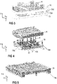
- the housing 7 comprises sidewalls 72 and a cover 74, wherein the cover 74 in this example is not yet mounted on the sidewalls 72.
- the sidewalls 72 form a closed frame.
- the frame formed by the sidewalls 72 has a rectangular cross-section. Other cross-sections such as, e.g., a square cross-section, however are also possible.
- the at least one substrate 10 is arranged inside and surrounded the frame formed by the sidewalls 72 in a horizontal plane.
- the sidewalls 72 can comprise a protrusion, for example, which presses the at least one substrate on a heat sink (heat sink not specifically illustrated in Figure 2 ).
- the housing comprises at least one strut 75 extending between two opposite sidewalls (e.g., between a first (longitudinal) sidewall and a second (longitudinal) sidewall opposite the first longitudinal side).
- Such struts 75 can also be used to press the one or more substrates 10 onto the heat sink 18.
- Struts 75 are exemplarily illustrated in Figures 6, 7, and 8 , for example.
- the cover 74 in the examples described herein comprises a top part, covering an opening formed by the sidewalls 72, and side parts which extend perpendicular to the top part and parallel to the sidewalls 72 of the housing when the cover 74 is arranged to close the opening formed by the sidewalls 72.
- the side parts of the cover 74 extend from the top part towards the at least one substrate 10 and the heat sink.
- the side parts may contact the sidewalls 72 and even the heat sink.
- the side parts may be permanently coupled to the heat sink in order to fix the cover 74 in place and prevent it from moving or even falling off.
- the cover 74 may be soldered, glued, or screwed to the heat sink 18.
- the side parts can also be omitted.
- a guiding element 76 is coupled to the sidewalls 72, and the cover 74 comprises a through hole 78.
- the guiding element 76 can comprise a pin, for example.
- the guiding element 76 may be inserted into the through hole 78 in order to correctly align the cover 74 and the sidewalls 72.
- the sidewalls 72 comprise one guiding element 76
- the cover 74 comprises one through hole 78. It is, however, also possible, that each of the sidewalls 72 and the cover 74 comprise more than one guiding element or through hole, respectively.
- the cover 74 when the cover 74 is arranged to close the opening formed by the sidewalls 72, the cover 74 exerts pressure on the sidewalls 72, thereby pressing the sidewalls 72 onto the at least one substrate 10, thereby pressing the at least one substrate 10 onto the heat sink (heat sink not specifically illustrated in Figure 3 ).
- the sidewalls 72 comprise a first contact area 792
- the cover 74 comprises a second contact area 794.
- the first contact area 792 directly contacts the second contact area 794.
- the first contact area 792 is formed by a surface of the sidewalls 72, in particular a surface of the sidewalls 72 which extends in parallel to the at least one substrate 10 and which forms a point of the sidewalls 72 that is arranged furthermost from the heat sink in the vertical direction y.
- the second contact area 794 is formed by a surface of the cover 74 which, when the cover 74 is mounted on the sidewalls 72 contacts the sidewalls 72 first.
- the power semiconductor module arrangement further comprises at least one press-on element 796 arranged between the cover 74 and the sidewalls 72. This is exemplarily illustrated in Figures 4 to 12 . Each of the at least one press-on element 796 provides a contact area for both the sidewalls 72 and the cover 74.
- each of the at least one press-on element 796 contacts the sidewalls 72, and with a second end, opposite the first end, each of the at least one press-on element 796 contacts the cover 74.
- Each of the at least one press-on element 796 is a flexible element that is compressed by the pressure that is exerted on the sidewalls 72 by the cover 74.
- a press-on element 796 can be firmly or detachably attached either to the sidewalls 72 or to the cover 74.
- a plurality of press-on elements 796 is arranged along the circumference of the frame formed by the sidewalls 72.
- the press-on elements 796 can be evenly distributed along the circumference.
- press-on elements 796 are flexible, pressure that is exerted by the cover 74 on the sidewalls 72 is evenly distributed along the entire circumference of the frame formed by the sidewalls 72. This is, because pressure exerted by the cover 74 is not instantly transferred to the sidewalls 72. Due to production tolerances, the cover 74 may contact different areas of the at least one press-on element 796 at different times during the mounting process. That is, the cover 74 may contact some areas of the at least one press-on element 796 first. Due to the pressure exerted by the cover 74, the respective press-on elements 796 or the respective area of the press-on element 796 are compressed. At this point, the pressure is not or only partly transferred to the sidewalls 72.
- the cover 74 contacts the remaining areas of the press-on elements 796, when the cover 74 is pressed more and more towards the sidewalls 72. Only when each of the press-on elements 796 is fully compressed, the entire pressure is transferred from the cover 74 via the press-on elements 796 to the sidewalls 72.
- Attaching the at least one press-on element 796 to the sidewalls 72 is only an example. According to another example, and as is exemplarily illustrated in Figure 5 , it is also possible to attach the press-on elements 796 to the cover 74 instead. The effect is identical in both cases. If the press-on elements 796 are attached to the cover 74 with a first side, a second side of the press-on elements 796 opposite the first side contacts the sidewalls 72 first. The press-on elements 796 are compressed by the pressure exerted by the cover 74 onto the sidewalls 72. Only when the press-on elements 796 are entirely compressed, the full amount of the pressure is transferred to the sidewalls 72. In this way, production tolerances and irregularities of the cover 74 and the sidewalls 72 can be compensated.
- each of the at least one press-on element 796 comprises an elastic material that can be compressed to a certain degree. That is, the press-on elements 796 can comprise a comparably soft material. According to one example, the at least one press-on element 796 has a hardness of between 15 Shore A and 100 Shore A.
- the at least one press-on element 796 can comprise at least one of a thermoplastic elastomer, silicone, and rubber.
- the press-on elements 796 can comprise or consist of EPDM (ethylene propylene diene monomer rubber), AEM (ethylene acrylic rubber), ACM (acrylic rubber or alkyl acrylate copolymer), FKM (fluorine rubber or fluorocarbon), VMQ (silicone rubber or vinyl methyl silicone), FVMQ (fluorosilicone rubber or fluorovinylmethylsiloxane rubber), PVMQ (phenyl methyl silicone rubber), or FFKM (perfluoroelastomeric compound having a higher amount of fluorine than FKM).
- EPDM ethylene propylene diene monomer rubber
- AEM ethylene acrylic rubber
- ACM acrylic rubber or alkyl acrylate copolymer
- FKM fluorine rubber or fluorocarbon
- VMQ silicone rubber or vinyl methyl silicone
- FVMQ fluorosilicone rubber or fluorovinylmethylsiloxane rubber
- PVMQ phenyl methyl silicone rubber
- the press-on elements 796 In an initial state, the press-on elements 796 have a first height in the vertical direction y.
- the initial state is the state in which no pressure is exerted on the press-on elements 796. This first height is reduced when pressure is exerted on the press-on elements 796. According to one example, the first height of the press-on elements 796 is reduced by 10 - 70% as compared to the initial state.
- each of the at least one press-on elements 796 is configured to transfer a pressure of between IN and 100N from the cover 74 to the sidewalls 72.
- each of a plurality of press-on elements 796 can have a round cross-section. That is, each of the at least one press-on element 796 can have a cylindrical shape, for example. This, however, is only an example.
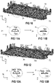
- the press-on elements 796 alternatively can have an angular (e.g., triangular, square, rectangular, or polygonal) or an oval cross-section, for example. Press-on elements 796 having an elongated shape are exemplarily illustrated in Figures 6, 7, 8 and 9 .
- the press-on elements 796 are mounted to the cover 74 instead of to the sidewalls 72 and are only partly visible, as the press-on elements 796 are partly concealed by the cover 74.
- a plurality of elongated press-on elements 796 is evenly distributed along the circumference of the frame formed by the sidewalls 72.
- each of the press-on elements 796 can have another shape such as cylindrical, oval or angular.
- Each of the plurality of press-on elements 796 can have the same height in the vertical direction y. In this way, the cover 74, when mounted onto the sidewalls 72, contacts all of the press-on elements 796 essentially at the same time. Any differences in height merely result from unintentional manufacturing tolerances.
- the frame formed by the sidewalls 72 has an essentially even height, and the press-on elements also have identical heights. According to another example which is not specifically illustrated, it is also possible that the height of the frame formed by the sidewalls 72 varies along its circumference. In this case it is possible that different press-on elements 796 have different heights. In any case, that side of each press-on element 796 which is arranged the furthest from the at least one substrate 10 and the heat sink 18 in the vertical direction, is arranged at the same distance from the heat sink 18, when the sidewalls 72 are arranged on the heat sink 18.
- the arrangement comprises a single press-on element 796 extending along the entire circumference of the frame formed by the sidewalls 72 without interruption.
- the press-on elements 796 illustrated in Figure 9 are similar to the press-on elements of the arrangement illustrated in Figure 6 .
- the press-on elements illustrated in Figure 9 are arranged on the cover 74 instead of on the sidewalls 72.
- press-on elements 796 on struts 75 extending between two opposite walls of the sidewalls 72.
- Press-on elements 796 can be arranged on struts 75 instead of or in addition to the press-on elements 796 arranged along the circumference of the frame formed by the sidewalls 72.
- the press-on elements 796 comprise a compressible material. This, however, is only an example. According to another example, a compression of the press-on elements 796 may result from a structural shape of the press-on elements 796. That is, the material of the press-on element 796 by itself may not be compressible, or may be compressible only marginally. However, the press-on element 796 may be bent or distorted under pressure.
- An example of such a press-on element 796 is schematically illustrated in Figures 10 and 11 .
- the press-on elements 796 as illustrated in Figures 10 and 11 comprise a base section 7962 and an arch-shaped section 7964 coupled to the base section 7962.
- a first end of the arch-shaped section 7964 is coupled to a first end of the base section 7962, and a second end of the arch-shaped section 7964 is coupled to a second end of the base section 7962.
- a middle section of the arch-shaped section 7964 extends and forms an arch between the first end and the second end.
- Figure 11A schematically illustrates one press-on element 796 in greater detail. As is schematically illustrated in Figure 11B , when pressure is exerted on the press-on element 796, the arch-shaped section 7964 is pressed towards the base section 7962.
- the arch-shaped section is interrupted at its topmost point. That is, a first curved brace 7966a extends from the first end of the base section 7962 towards a second curved brace 7966b. The second curved brace 7966b in turn extends from the second end of the base section 7962 towards the first curved brace 7966a. The first curved brace 7966a and the second curved brace 7966b, however, do not contact each other. As is illustrated in Figure 13B , the curved braces 7966a, 7966b are bent towards the base section 7962 when pressure is exerted on the press-on element 796.
- Figure 13A illustrates the press-on element 796 in an initial state when no pressure is exerted on the press-on element 796.
- press-on elements 796 illustrated in Figures 10 to 13 are only examples.
- the press-on elements 796 can have any other suitable shape that allows the press-on element 796 to be bent or distorted under pressure.
- the at least one press-on element 796 can comprise any kind of spring element.
- the press-on elements 796 can be firmly or detachably attached to either the sidewalls 72 or the cover 74.
- the press-on elements 796 can be formed directly on the sidewalls 72 or the cover 74 by any kind of injection molding process. It is, however, also possible to manufacture the press-on elements 796 separately.
- the press-on elements may then be fixed to the sidewalls 72 or the cover 74 in any suitable way.
- the press-on elements 796 can be glued to the sidewalls 72 or the cover 74, or can be inserted into corresponding slots or cavities formed in the sidewalls 72 or in the cover 74.
- the at least one substrate 10 and the sidewalls 72 of the housing are directly mounted to a heat sink 18.
- a base plate is arranged between the at least one substrate, the housing and the heat sink. That is, the at least one substrate 10 may be pressed onto the base plate by means of the housing. The base plate may be attached to a heat sink.
Landscapes
- Cooling Or The Like Of Semiconductors Or Solid State Devices (AREA)
Priority Applications (3)
| Application Number | Priority Date | Filing Date | Title |
|---|---|---|---|
| EP21167227.4A EP4071793A1 (de) | 2021-04-07 | 2021-04-07 | Leistungshalbleitermodulanordnung und gehäuse für eine leistungshalbleitermodulanordnung |
| US17/714,625 US20220328368A1 (en) | 2021-04-07 | 2022-04-06 | Power semiconductor module arrangement and housing for a power semiconductor module arrangement |
| CN202210373733.4A CN115206889A (zh) | 2021-04-07 | 2022-04-07 | 功率半导体模块装置和用于功率半导体模块装置的外壳 |
Applications Claiming Priority (1)
| Application Number | Priority Date | Filing Date | Title |
|---|---|---|---|
| EP21167227.4A EP4071793A1 (de) | 2021-04-07 | 2021-04-07 | Leistungshalbleitermodulanordnung und gehäuse für eine leistungshalbleitermodulanordnung |
Publications (1)
| Publication Number | Publication Date |
|---|---|
| EP4071793A1 true EP4071793A1 (de) | 2022-10-12 |
Family
ID=75426495
Family Applications (1)
| Application Number | Title | Priority Date | Filing Date |
|---|---|---|---|
| EP21167227.4A Pending EP4071793A1 (de) | 2021-04-07 | 2021-04-07 | Leistungshalbleitermodulanordnung und gehäuse für eine leistungshalbleitermodulanordnung |
Country Status (3)
| Country | Link |
|---|---|
| US (1) | US20220328368A1 (de) |
| EP (1) | EP4071793A1 (de) |
| CN (1) | CN115206889A (de) |
Families Citing this family (2)
| Publication number | Priority date | Publication date | Assignee | Title |
|---|---|---|---|---|
| EP3951851A1 (de) * | 2020-08-05 | 2022-02-09 | Siemens Aktiengesellschaft | Leistungshalbleitermodulsystem und herstellungsverfahren für ein leistungshalbleitermodulsystem |
| DE102024201720A1 (de) * | 2024-02-26 | 2025-08-28 | Robert Bosch Gesellschaft mit beschränkter Haftung | Leistungsmodul mit einem Schaltungsträger |
Citations (5)
| Publication number | Priority date | Publication date | Assignee | Title |
|---|---|---|---|---|
| JPH08274204A (ja) * | 1995-03-23 | 1996-10-18 | Texas Instr Inc <Ti> | ハーメチックシールシステムおよびデバイスのハーメチックシール方法 |
| KR20050042373A (ko) * | 2003-11-03 | 2005-05-09 | 삼성전기주식회사 | 리크를 방지할 수 있는 세라믹 패키지 밀봉 구조, 리크를방지할 수 있는 세라믹 패키지 및 상기 세라믹 패키지의제조 방법 |
| US20120106086A1 (en) * | 2010-10-28 | 2012-05-03 | Infineon Technologies Ag | Semiconductor module having an insert and method for producing a semiconductor module having an insert |
| US20200091023A1 (en) * | 2018-09-19 | 2020-03-19 | Infineon Technologies Ag | Power Semiconductor Module Arrangement and Housing for a Power Semiconductor Arrangement |
| US10763468B2 (en) * | 2017-04-25 | 2020-09-01 | Commissariat à l'énergie atomique et aux énergies alternatives | Sealing cell and method for encapsulating a microelectronic component with such a sealing cell |
Family Cites Families (2)
| Publication number | Priority date | Publication date | Assignee | Title |
|---|---|---|---|---|
| US7851267B2 (en) * | 2007-10-18 | 2010-12-14 | Infineon Technologies Ag | Power semiconductor module method |
| DE102017110722B4 (de) * | 2017-05-17 | 2021-03-18 | Semikron Elektronik Gmbh & Co. Kg | Leistungselektronische Anordnung und elektrisches Fahrzeug hiermit |
-
2021
- 2021-04-07 EP EP21167227.4A patent/EP4071793A1/de active Pending
-
2022
- 2022-04-06 US US17/714,625 patent/US20220328368A1/en active Pending
- 2022-04-07 CN CN202210373733.4A patent/CN115206889A/zh active Pending
Patent Citations (7)
| Publication number | Priority date | Publication date | Assignee | Title |
|---|---|---|---|---|
| JPH08274204A (ja) * | 1995-03-23 | 1996-10-18 | Texas Instr Inc <Ti> | ハーメチックシールシステムおよびデバイスのハーメチックシール方法 |
| US5641713A (en) * | 1995-03-23 | 1997-06-24 | Texas Instruments Incorporated | Process for forming a room temperature seal between a base cavity and a lid using an organic sealant and a metal seal ring |
| KR20050042373A (ko) * | 2003-11-03 | 2005-05-09 | 삼성전기주식회사 | 리크를 방지할 수 있는 세라믹 패키지 밀봉 구조, 리크를방지할 수 있는 세라믹 패키지 및 상기 세라믹 패키지의제조 방법 |
| US20050139990A1 (en) * | 2003-11-03 | 2005-06-30 | Samsung Electro-Mechanics Co., Ltd. | Method of manufacturing ceramic package sealing structure and ceramic package having said sealing structure |
| US20120106086A1 (en) * | 2010-10-28 | 2012-05-03 | Infineon Technologies Ag | Semiconductor module having an insert and method for producing a semiconductor module having an insert |
| US10763468B2 (en) * | 2017-04-25 | 2020-09-01 | Commissariat à l'énergie atomique et aux énergies alternatives | Sealing cell and method for encapsulating a microelectronic component with such a sealing cell |
| US20200091023A1 (en) * | 2018-09-19 | 2020-03-19 | Infineon Technologies Ag | Power Semiconductor Module Arrangement and Housing for a Power Semiconductor Arrangement |
Also Published As
| Publication number | Publication date |
|---|---|
| CN115206889A (zh) | 2022-10-18 |
| US20220328368A1 (en) | 2022-10-13 |
Similar Documents
| Publication | Publication Date | Title |
|---|---|---|
| US11533824B2 (en) | Power semiconductor module and a method for producing a power semiconductor module | |
| US12500152B2 (en) | Power semiconductor module, method for assembling a power semiconductor module and housing for a power semiconductor module | |
| US11699625B2 (en) | Power semiconductor module arrangement | |
| US11581230B2 (en) | Power semiconductor module and a method for producing a power semiconductor module | |
| US20220328368A1 (en) | Power semiconductor module arrangement and housing for a power semiconductor module arrangement | |
| EP4084062A1 (de) | Leistungshalbleitermodulanordnung | |
| EP4307359A1 (de) | Leistungshalbleitermodulanordnung und verfahren zur herstellung davon | |
| US11856718B2 (en) | Housing for a power semiconductor module arrangement | |
| EP3736854A1 (de) | Leistungshalbleitermodulanordnung | |
| EP4050650A1 (de) | Leistungshalbleitermodulanordnung | |
| US20260090385A1 (en) | Semiconductor module comprising a housing | |
| US20260053056A1 (en) | Housing and semiconductor module having a housing | |
| US12482725B2 (en) | Power semiconductor module arrangements and methods for producing power semiconductor module arrangements | |
| EP4439649A1 (de) | Substratanordnung | |
| US20250273520A1 (en) | Housing, semiconductor module having a housing, and method for assembling a semiconductor module | |
| EP4421868A1 (de) | Halbleitermodulanordnung | |
| US12456654B2 (en) | Power semiconductor modules | |
| EP4422358A1 (de) | Substrat | |
| EP4607584A1 (de) | Halbleitermodulanordnung | |
| US20230253291A1 (en) | Power semiconductor module arrangement and methods for producing a semiconductor arrangement | |
| EP4345884A1 (de) | Leistungshalbleitermodulanordnung und leiterplatte für eine leistungshalbleitermodulanordnung |
Legal Events
| Date | Code | Title | Description |
|---|---|---|---|
| PUAI | Public reference made under article 153(3) epc to a published international application that has entered the european phase |
Free format text: ORIGINAL CODE: 0009012 |
|
| STAA | Information on the status of an ep patent application or granted ep patent |
Free format text: STATUS: REQUEST FOR EXAMINATION WAS MADE |
|
| 17P | Request for examination filed |
Effective date: 20220127 |
|
| AK | Designated contracting states |
Kind code of ref document: A1 Designated state(s): AL AT BE BG CH CY CZ DE DK EE ES FI FR GB GR HR HU IE IS IT LI LT LU LV MC MK MT NL NO PL PT RO RS SE SI SK SM TR |
|
| STAA | Information on the status of an ep patent application or granted ep patent |
Free format text: STATUS: EXAMINATION IS IN PROGRESS |
|
| 17Q | First examination report despatched |
Effective date: 20250130 |