EP4071992A1 - Isoliertransformator und damit ausgerüstete leistungswandlervorrichtung - Google Patents
Isoliertransformator und damit ausgerüstete leistungswandlervorrichtung Download PDFInfo
- Publication number
- EP4071992A1 EP4071992A1 EP19954762.1A EP19954762A EP4071992A1 EP 4071992 A1 EP4071992 A1 EP 4071992A1 EP 19954762 A EP19954762 A EP 19954762A EP 4071992 A1 EP4071992 A1 EP 4071992A1
- Authority
- EP
- European Patent Office
- Prior art keywords
- sub
- terminal
- terminals
- winding
- windings
- Prior art date
- Legal status (The legal status is an assumption and is not a legal conclusion. Google has not performed a legal analysis and makes no representation as to the accuracy of the status listed.)
- Pending
Links
Images




Classifications
-
- H—ELECTRICITY
- H02—GENERATION; CONVERSION OR DISTRIBUTION OF ELECTRIC POWER
- H02M—APPARATUS FOR CONVERSION BETWEEN AC AND AC, BETWEEN AC AND DC, OR BETWEEN DC AND DC, AND FOR USE WITH MAINS OR SIMILAR POWER SUPPLY SYSTEMS; CONVERSION OF DC OR AC INPUT POWER INTO SURGE OUTPUT POWER; CONTROL OR REGULATION THEREOF
- H02M3/00—Conversion of DC power input into DC power output
- H02M3/22—Conversion of DC power input into DC power output with intermediate conversion into AC
- H02M3/24—Conversion of DC power input into DC power output with intermediate conversion into AC by static converters
- H02M3/28—Conversion of DC power input into DC power output with intermediate conversion into AC by static converters using discharge tubes with control electrode or semiconductor devices with control electrode to produce the intermediate AC
- H02M3/325—Conversion of DC power input into DC power output with intermediate conversion into AC by static converters using discharge tubes with control electrode or semiconductor devices with control electrode to produce the intermediate AC using devices of a triode or a transistor type requiring continuous application of a control signal
- H02M3/335—Conversion of DC power input into DC power output with intermediate conversion into AC by static converters using discharge tubes with control electrode or semiconductor devices with control electrode to produce the intermediate AC using devices of a triode or a transistor type requiring continuous application of a control signal using semiconductor devices only
- H02M3/33569—Conversion of DC power input into DC power output with intermediate conversion into AC by static converters using discharge tubes with control electrode or semiconductor devices with control electrode to produce the intermediate AC using devices of a triode or a transistor type requiring continuous application of a control signal using semiconductor devices only having several active switching elements
- H02M3/33576—Conversion of DC power input into DC power output with intermediate conversion into AC by static converters using discharge tubes with control electrode or semiconductor devices with control electrode to produce the intermediate AC using devices of a triode or a transistor type requiring continuous application of a control signal using semiconductor devices only having several active switching elements having at least one active switching element at the secondary side of an isolation transformer
- H02M3/33584—Bidirectional converters
-
- H—ELECTRICITY
- H01—ELECTRIC ELEMENTS
- H01F—MAGNETS; INDUCTANCES; TRANSFORMERS; SELECTION OF MATERIALS FOR THEIR MAGNETIC PROPERTIES
- H01F38/00—Adaptations of transformers or inductances for specific applications or functions
-
- H—ELECTRICITY
- H01—ELECTRIC ELEMENTS
- H01F—MAGNETS; INDUCTANCES; TRANSFORMERS; SELECTION OF MATERIALS FOR THEIR MAGNETIC PROPERTIES
- H01F38/00—Adaptations of transformers or inductances for specific applications or functions
- H01F38/08—High-leakage transformers or inductances
-
- H—ELECTRICITY
- H02—GENERATION; CONVERSION OR DISTRIBUTION OF ELECTRIC POWER
- H02M—APPARATUS FOR CONVERSION BETWEEN AC AND AC, BETWEEN AC AND DC, OR BETWEEN DC AND DC, AND FOR USE WITH MAINS OR SIMILAR POWER SUPPLY SYSTEMS; CONVERSION OF DC OR AC INPUT POWER INTO SURGE OUTPUT POWER; CONTROL OR REGULATION THEREOF
- H02M1/00—Details of apparatus for conversion
- H02M1/44—Circuits or arrangements for compensating for electromagnetic interference in converters or inverters
-
- H—ELECTRICITY
- H01—ELECTRIC ELEMENTS
- H01F—MAGNETS; INDUCTANCES; TRANSFORMERS; SELECTION OF MATERIALS FOR THEIR MAGNETIC PROPERTIES
- H01F38/00—Adaptations of transformers or inductances for specific applications or functions
- H01F2038/006—Adaptations of transformers or inductances for specific applications or functions matrix transformer consisting of several interconnected individual transformers working as a whole
Definitions
- Patent Literature 1 WO 2018/016106 A1
- a main object of the present invention is to provide a low-cost insulating transformer having the high assemblability and heat dissipation, and a power conversion device including the insulating transformer.
- An insulating transformer of the present invention includes first to Nth sub-insulating transformers electrically connected to each other.
- N is an integer greater than or equal to 2.
- Each of the first to Nth sub-insulating transformers includes first and second sub-windings, first and second sub-terminals connected to a first polarity terminal and a second polarity terminal of the first sub-winding, respectively, and third and fourth sub-terminals connected to a first polarity terminal and a second polarity terminal of the second sub-winding, respectively.
- Polarity directions of the first and second sub-windings are identical.
- Each of the first to Nth sub-insulating transformers is configured such that an excitation inductance of the first sub-winding and an excitation inductance of the second sub-winding become opposite polarities when a current flows from the first sub-terminal to the third sub-terminal through the first sub-winding, an interphase capacitance between the first and second sub-windings, and the second sub-winding.
- the insulating transformer is divided into a plurality of sub-insulating transformers. Accordingly, an increase in volume and weight concentration can be prevented in the insulating transformer, the assemblability can be improved by enabling substrate mounting, the heat dissipation can be improved by dispersing the heat source, and the cost reduction can be implemented using a general-purpose sub-insulating transformer with a large distribution amount and easy availability.
- Each of the first to Nth sub-insulating transformers is configured such that the excitation inductance of the first sub-winding and the excitation inductance of the second sub-winding become opposite polarities when the current flows from the first sub-terminal to the third sub-terminal through the first sub-winding, the interphase capacitance between the first and second sub-windings, and the second sub-winding. Accordingly, the sum of the excitation inductances of the first and second windings can be reduced, and generation of a resonance phenomenon between the excitation inductances of the first and second windings and the interphase capacitance can be prevented.
- FIG. 1 is a circuit block diagram illustrating a configuration of a bidirectional DC/DC converter according to a first embodiment.
- the bidirectional DC/DC converter (power conversion device) is a dual active bridge (DAB) system, and includes DC terminals T1 to T4, current detectors 1, 7, power converters 2, 6, an insulating transformer 3, an operation unit 8, and a control device 9.
- DAB dual active bridge
- DC terminals T1, T2 are connected to positive and negative electrodes of a DC power supply 21 (first DC power supply), respectively.
- DC terminals T3, T4 are connected to positive and negative electrodes of a DC power supply 22 (second DC power supply), respectively.
- Each of a DC voltage VDC1 between DC terminals T1, T2 and a DC voltage VDC2 between DC terminals T3, T4 is detected by control device 9.
- one of DC power supplies 21, 22 is a solar cell that outputs DC power, and the other is a battery (or capacitor) that stores the DC power.
- Both of DC power supplies 21, 22 may be a battery (or capacitor).
- a load driven by the DC power may be connected in parallel to at least one of DC power supplies 21, 22.
- Insulating transformer 3 includes first and second main windings 4, 5 and first to fourth main terminals 3a to 3d.
- a black circle (•) is marked on a positive polarity side of each of first and second main windings 4, 5.
- a positive electrode terminal (first polarity terminal) and a negative electrode terminal (second polarity terminal) of first main winding 4 are connected to first and second main terminals 3a, 3b, respectively.
- the positive electrode terminal and the negative electrode terminal of second main winding 5 are connected to third and fourth main terminals 3c, 3d, respectively.
- FIG. 1 illustrates a case where the polarity directions of first and second main windings 4, 5 are both an upward direction. Numbers of turns of first and second main windings 4, 5 are the same.
- AC voltage VAC1 When an AC voltage VAC1 is applied between first and second main terminals 3a, 3b, an AC voltage VAC2 appears between third and fourth main terminals 3c, 3d. Conversely, when an AC voltage VAC2 is provided between third and fourth main terminals 3c, 3d, AC voltage VAC1 appears between first and second main terminals 3a, 3b.
- AC voltages VAC1, VAC2 have the same polarity (that is, the same phase) and the same amplitude.
- Power converter 2 (first power converter) includes DC terminals 2a, 2b respectively connected to DC terminals T1, T2, and AC terminals 2c, 2d respectively connected to first and second main terminals 3a, 3b of insulating transformer 3, and is controlled by control device 9.
- power converter 2 converts DC voltage VDC1 applied from DC power supply 21 to DC terminals 2a, 2b into AC voltage VAC1 and outputs AC voltage VAC1 between AC terminals 2c, 2d.
- power converter 2 converts AC voltage VAC1 applied between AC terminals 2c, 2d into DC voltage VDC1 and outputs DC voltage VDC1 between DC terminals 2a, 2b.
- Power converter 6 (second power converter) includes DC terminals 6a, 6b connected to DC terminals T3, T4, and AC terminals 6c, 6d connected to third and fourth main terminals 3c, 3d of insulating transformer 3, and is controlled by control device 9.
- power converter 6 converts AC voltage VAC2 provided between AC terminals 6c, 6d into DC voltage VDC2 and outputs DC voltage VDC2 between DC terminals 6a, 6b.
- power converter 6 converts DC voltage VDC2 applied from DC power supply 22 to DC terminals 6a, 6b into AC voltage VAC2 and outputs AC voltage VAC2 between AC terminals 6c, 6d.
- Current detector 1 detects a current I1 flowing between DC terminal T1 and DC terminal 2a of power converter 2, and outputs a signal I1f indicating a detected value of current I1 to control device 9.
- Current detector 7 detects a current 12 flowing between DC terminal T3 and DC terminal 6a of power converter 6, and outputs a signal I2f indicating a detected value of current 12 to control device 9.
- Operation unit 8 includes a plurality of buttons and a plurality of switches operated by a user of the bidirectional DC/DC converter and an image display unit that displays various pieces of information. By operating operation unit 8, the user can turn on and off the power of the bidirectional DC/DC converter and select one of the first and second transmission modes. Operation unit 8 outputs a signal indicating the selected transmission mode or the like to control device 9.
- Control device 9 controls the entire bidirectional DC/DC converter based on DC voltages VDC1, VDC2, DC currents I1, I2 indicated by the output signals of current detectors 1, 7, the signal from operation unit 8, and the like.
- control device 9 controls each of power converters 2, 6 such that DC current 12 becomes a predetermined reference current I2R (or DC voltage VDC2 becomes a predetermined reference voltage VDC2R).
- control device 9 controls each of power converters 2, 6 such that DC current I1 becomes a predetermined reference current I1R (or DC voltage VDC1 becomes a predetermined reference voltage VDC1R).
- Control device 9 includes a processing circuit 9a.
- Processing circuit 9a may be configured by a digital electronic circuit such as an arithmetic processing device and a storage device, configured by an analog electronic circuit such as a comparator, an operational amplifier, and a differential amplifier circuit, or configured by both the digital electronic circuit and the analog electronic circuit.
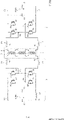
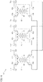
- FIG. 2 is a circuit diagram illustrating a configuration of insulating transformer 3.
- insulating transformer 3 includes a plurality of sub-insulating transformers 11 to 13.
- Sub-insulating transformers 11 to 13 configure first to Nth sub-insulating transformers.
- N is an integer greater than or equal to 2.
- First sub-insulating transformer 11 includes an iron core (not illustrated), first and second sub-windings 14, 17 wound around the iron core, and first to fourth sub-terminals 11a to 11d.
- a black circle (•) is marked on the positive polarity side of each of first and second sub-windings 14, 17.
- the positive electrode terminal and the negative electrode terminal of first sub-winding 14 are connected to first and second sub-terminals 11a, 11b, respectively.
- the positive electrode terminal and the negative electrode terminal of second sub-winding 17 are connected to third and fourth sub-terminals 11c, 11d, respectively.
- FIG. 2 illustrates the case where the polarity directions of first and second sub-windings 14, 17 are both the upward direction.
- the numbers of turns of first and second sub-windings 14, 17 are the same.
- Second sub-insulating transformer 12 includes an iron core (not illustrated), first and second sub-windings 15, 18 wound around the iron core, and first to fourth sub-terminals 12a to 12d.
- a black circle (•) is marked on the positive polarity side of each of first and second sub-windings 15, 18.
- the positive electrode terminal and the negative electrode terminal of first sub-winding 15 are connected to first and second sub-terminals 12a, 12b, respectively.
- the positive electrode terminal and the negative electrode terminal of second sub-winding 18 are connected to third and fourth sub-terminals 12c, 12d, respectively.
- FIG. 2 illustrates the case where the polarity directions of first and second sub-windings 15, 18 are both the upward direction.
- the numbers of turns of first and second sub-windings 15, 18 are the same.
- Third sub-insulating transformer 13 includes an iron core (not illustrated), first and second sub-windings 16, 19 wound around the iron core, and first to fourth sub-terminals 13a to 13d.
- a black circle (•) is marked on the positive polarity side of each of first and second sub-windings 16, 19.
- the positive electrode terminal and the negative electrode terminal of first sub-winding 16 are connected to first and second sub-terminals 13a, 13b, respectively.
- the positive electrode terminal and the negative electrode terminal of second sub-winding 19 are connected to third and fourth sub-terminals 13c, 13d, respectively.
- FIG. 2 illustrates the case where the polarity directions of first and second sub-windings 16, 19 are both the upward direction.
- the numbers of turns of first and second sub-windings 16, 19 are the same.
- first sub-terminal 11a of first sub-insulating transformer 11 is connected to first main terminal 3a of insulating transformer 3.
- Second sub-terminal 11b of first sub-insulating transformer 11 is connected to first sub-terminal 12a of second sub-insulating transformer 12.
- Second sub-terminal 12b of second sub-insulating transformer 12 is connected to first sub-terminal 13a of third sub-insulating transformer 13.
- Second sub-terminal 13b of third sub-insulating transformer 13 is connected to second main terminal 3b of insulating transformer 3.
- the polarities of three second sub-windings 17 to 19 are oriented in the same direction.
- Three second sub-windings 17 to 19 are connected in series between third and fourth main terminals 3c, 3d of insulating transformer 3 to configure second main winding 5. That is, third sub-terminal 11c of first sub-insulating transformer 11 is connected to third main terminal 3c of insulating transformer 3.
- Fourth sub-terminal 11d of first sub-insulating transformer 11 is connected to third sub-terminal 12c of second sub-insulating transformer 12.
- Fourth sub-terminal 12d of second sub-insulating transformer 12 is connected to third sub-terminal 13c of third sub-insulating transformer 13.
- Fourth sub-terminal 13d of third sub-insulating transformer 13 is connected to fourth main terminal 3d of insulating transformer 3.
- AC voltage VAC1 When AC voltage VAC1 is applied between first main terminal 3a and second main terminal 3b, AC voltage VAC2 appears between third main terminal 3c and fourth main terminal 3d. When AC voltage VAC2 is applied between third main terminal 3c and fourth main terminal 3d, AC voltage VAC1 appears between first main terminal 3a and second main terminal 3b. Because the number of turns of first main winding 4 and the number of turns of second main winding 5 are the same, the amplitude of AC voltage VAC1 and the amplitude of AC voltage VAC2 are the same.
- AC voltages VAC1, VAC2 have the same polarity, and the phase of AC voltage VAC1 and the phase of AC voltage VAC2 are the same.
- the plurality of sub-insulating transformers 11 to 13 are connected in series to configure one insulating transformer 3, an increase in volume and weight concentration can be prevented to enable substrate mounting to improve assemblability, heat dissipation can be improved by dispersing a heat source, and cost reduction can be improved using a general-purpose core having a large distribution amount and high availability.
- the polarity directions of sub-windings 14 to 19 are aligned in the same direction, generation of a resonance phenomenon can be prevented in the bidirectional DC/DC converter. The reason why the resonance phenomenon can be prevented will be described later.
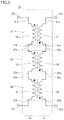
- FIG. 3 is a circuit diagram illustrating a configuration of power converters 2, 6.
- power converter 2 includes a capacitor C1, insulated gate bipolar transistors (IGBTs) Q1 to Q4, diodes D1 to D4, and reactors L1, L2.
- Capacitor C1 is connected between DC terminals T1, T2, and smooths and stabilizes DC voltage VDC1 between DC terminals T1, T2.
- Collectors of the IGBTs Q1, Q2 are connected to DC terminal T1, and emitters of IGBTs Q1, Q2 are connected to nodes N1, N2 (first and second AC terminals).
- Collectors of IGBTs Q3, Q4 are connected to nodes N1, N2, and emitters of IGBTs Q3, Q4 are connected to DC terminal T2.
- Each of IGBTs Q1 to Q4 is turned on and off by control device 9.
- Reactor L1 is connected between node N1 and first main terminal 3a of insulating transformer 3.
- Reactor L2 is connected between node N2 and second main terminal 3b of insulating transformer 3.
- Each of reactors L1, L2 stores electromagnetic energy.
- Power converter 6 includes reactors L3 to L5, IGBTs Q5 to Q8, diodes D5 to D8, and a capacitor C2.
- Reactor L3 is connected between third main terminal 3c of insulating transformer 3 and a node N4.
- Reactor L4 is connected between fourth main terminal 3d of insulating transformer 3 and a node N3.
- Each of reactors L3, L4 stores electromagnetic energy.
- IGBTs Q5, Q6 are connected to each other, and emitters of IGBTs Q5, Q6 are connected to nodes N3, N4. Collectors of IGBTs Q7, Q8 are connected to nodes N3, N4, and emitters of IGBTs Q7, Q8 are connected to DC terminal T4. Each of IGBTs Q5 to Q8 is turned on and off by control device 9.
- Capacitor C2 is connected between the collectors of IGBTs Q5, Q6 and DC terminal T4.
- Reactor L5 is connected between the collectors of IGBTs Q5, Q6 and DC terminal T3. Capacitor C2 and reactor L5 configure a low-pass filter.
- a metal oxide semiconductor field effect transistor may be used instead of the IGBT.
- MOSFET metal oxide semiconductor field effect transistor
- a capacitor may be connected in parallel to the IGBT as a zero voltage switching circuit that makes the voltage between the collector and the emitter of the IGBT during switching substantially zero.
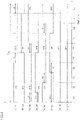
- FIG. 4 is a time chart illustrating the operation of the bidirectional DC/DC converter in FIGS. 1 to 3 .
- FIG. 4 illustrates the operation in the first transmission mode in which DC power is transmitted from DC power supply 21 to DC power supply 22.
- DC power supply 22 is a battery.
- FIGS. 4(A) to 4(H) indicate on and off operations of IGBTs Q1, Q3, Q2, Q4, Q5, Q7, Q6, Q8, respectively.
- a switching period Tsw of IGBT Q1 is divided into 10 periods TA to TJ.
- control device 9 In the first transmission mode, control device 9 alternately turns on IGBT Q1, Q3, IGBTs Q4, Q2, and IGBTs Q5, Q7 within switching period Tsw with a short-circuit prevention time td interposed therebetween, and fixes IGBTs Q6, Q8 to an off state.
- a period from turn-off of IGBT Q2 to turn-on of IGBT Q4 is defined as a first phase shift amount ⁇ 1
- a period from turn-off of IGBT Q2 to turn-on of IGBT Q7 is defined as a second phase shift amount ⁇ 2.
- Control device 9 adjusts first phase shift amount ⁇ 1 and second phase shift amount ⁇ 2 based on a transmission power amount.
- second phase shift amount ⁇ 2 is set to a value larger than first phase shift amount ⁇ 1.
- second phase shift amount ⁇ 2 is set to the same value as first phase shift amount ⁇ 1.
- IGBTs Q1, Q4 are turned on, the current flows from the positive electrode of DC power supply 21 to the negative electrode of DC power supply 21 through IGBT Q1, reactor L1, first main winding 4, reactor L2, and IGBT Q4, and the electromagnetic energy is stored in reactors L1, L2.
- IGBT Q5 is turned on, the current flows from third main terminal 3c of insulating transformer 3 to third terminal 3c through reactor L3, diode D6, IGBT Q5, reactor L4, and second main winding 5, and the electromagnetic energy is stored in reactors L3, L4.
- IGBTs Q1, Q4 are maintained in an on state, the current flows in the same path as in period TB, and the electromagnetic energy is stored in reactors L1, L2.
- IGBT Q5 is turned off, the current flows from third terminal 3c of insulating transformer 3 to third terminal 3c through reactor L3, diode D6, reactor L5, DC power supply 22 (battery), diode D7, reactor L4, and second main winding 5 of insulating transformer 3, and the electromagnetic energy of reactors L3, L4 is released.
- control device 9 In the second transmission mode in which the DC power is transmitted from DC power supply 22 to DC power supply 21, control device 9 alternately turns on IGBTs Q6, Q8, IGBTs Q7, Q5, and IGBTs Q2, Q4 with a short-circuit prevention time td interposed therebetween, and fixes IGBTs Q1, Q3 to the off state. In the second transmission mode, because the reverse operation of the first transmission mode is performed, the description thereof is not repeated.
- the plurality of sub-insulating transformers 11 to 13 are connected in series to configure one insulating transformer 3, so that the assemblability, the heat dissipation, and the cost reduction can be improved to achieve the high performance of the product.
- FIG. 5 is a circuit diagram illustrating a main part of a comparative example of the first embodiment, and is a view compared with FIG. 2 .
- an insulating transformer 25 is used in the comparative example.
- Insulating transformer 25 includes first to fourth main terminals 25a to 25d and a plurality of sub-insulating transformers 31 to 33.
- the plurality of sub-insulating transformers 31 to 33 are connected in series between first and third main terminals 25a, 25c and second and fourth main terminals 25b, 25d.
- first sub-insulating transformer 31 includes an iron core (not illustrated), first and second sub-windings 34, 37 wound around the iron core, and first to fourth sub-terminals 31a to 31d.
- a black circle (•) is marked on the positive polarity side of each of first and second sub-windings 34, 37.
- the positive electrode terminal and the negative electrode terminal of first sub-winding 34 are connected to first and second sub-terminals 31a, 31b, respectively.
- the positive electrode terminal and the negative electrode terminal of second sub-winding 37 are connected to fourth and third sub-terminals 31d and 31c, respectively.
- FIG. 5 illustrates the case where the polarity directions of first and second sub-windings 34, 37 are the upward direction and the downward direction, respectively.
- the numbers of turns of first and second sub-windings 34, 37 are the same.
- Second sub-insulating transformer 32 includes an iron core (not illustrated), first and second sub-windings 35, 38 wound around the iron core, and first to fourth sub-terminals 32a to 32d.
- a black circle (•) is marked on the positive polarity side of first and second sub-windings 35, 38.
- the positive electrode terminal and the negative electrode terminal of first sub-winding 35 are connected to first and second sub-terminals 32a, 32b, respectively.
- the positive electrode terminal and the negative electrode terminal of second sub-winding 38 are connected to fourth and third sub-terminals 32d, 32c, respectively.
- FIG. 5 illustrates the case where the polarity directions of the first and second sub-windings 35, 38 are the upward direction and the downward direction, respectively.
- the numbers of turns of first and second sub-windings 35, 38 are the same.
- Third sub-insulating transformer 33 includes an iron core (not illustrated), first and second sub-windings 36, 39 wound around the iron core, and first to fourth sub-terminals 33a to 33d.
- a black circle (•) is marked on the positive polarity side of each of first and second sub-windings 36, 39.
- the positive electrode terminal and the negative electrode terminal of first sub-winding 36 are connected to first and second sub-terminals 33a, 33b, respectively.
- the positive electrode terminal and the negative electrode terminal of second sub-winding 39 are connected to fourth and third sub-terminals 33d, 33c, respectively.
- FIG. 5 illustrates the case where the polarity directions of first and second sub-windings 36, 39 are the upward direction and the downward direction, respectively.
- the number of turns of first and second sub-windings 36, 39 are the same.
- first sub-windings 34 to 36 are oriented upward.
- Three first sub-windings 34 to 36 are connected in series between first and second main terminals 25a, 25b of insulating transformer 25 to configure a first main winding 26.
- the polarities of three second sub-windings 37 to 39 are directed downward.
- Three second sub-windings 37 to 39 are connected in series between third and fourth main terminals 25c, 25d of insulating transformer 25 to configure a second main winding 27.
- AC voltage VAC1 When AC voltage VAC1 is applied between first main terminal 25a and second main terminal 25b, AC voltage VAC2 appears between third main terminal 25c and fourth main terminal 25d. When AC voltage VAC2 is applied between third main terminal 25c and fourth main terminal 25d, AC voltage VAC1 appears between first main terminal 25a and second main terminal 25b. Because the number of turns of first main winding 26 and the number of turns of second main winding 27 are the same, the amplitude of AC voltage VAC1 and the amplitude of AC voltage VAC2 are the same.
- AC voltages VAC1, VAC2 have opposite polarities, and the phase of AC voltage VAC1 and the phase of AC voltage VAC2 are shifted by 180 degrees.
- Each of sub-terminals 31b, 32a and sub-terminals 31d, 32c to which sub-insulating transformers 31, 32 are connected is a high-impedance connection point to which an electrical component other than sub-insulating transformers 31, 32 is not connected.
- Each of sub-terminals 32b, 33a and sub-terminals 32d, 33c to which sub-insulating transformers 32, 33 are connected is a high-impedance connection point to which an electrical component other than sub-insulating transformers 32, 33 is not connected.
- the interphase capacitance between the first and second sub-windings of sub-insulating transformer 31 to 33 becomes apparent at the connection point of insulating transformer 31 to 33, and the resonance phenomenon is generated in a path passing through the first and second sub-windings and the interphase capacitance therebetween.
- FIG. 6 is the circuit diagram illustrating a configuration of the bidirectional DC/DC converter including insulating transformer 25 in FIG. 5 , and is a view compared with FIG. 3 .
- first to fourth main terminals 25a to 25d of insulating transformer 25 are connected to one terminals of reactors L1 to L4, and the other terminals of reactors L1 to L4 are connected to nodes N1 to N4.
- an earth capacitance C3 is connected between DC terminal T2 and a line (a line of the reference voltage) of a ground voltage GND
- an earth capacitance C4 is connected between DC terminal T4 and the line of ground voltage GND
- Earth capacitances C3, C4 assume the case where each of DC terminals T2, T4 is connected to a grounded housing with a capacitor interposed therebetween. However, this represents the state in which DC terminals T2, T4 are coupled to each other through an electrically low-impedance path.
- Each of DC terminals T2, T4 may be directly connected to the housing without interposing the capacitor therebetween, and the housing may be grounded.
- each of DC terminals T2, T4 may be connected to a power system in which a ground potential is defined with an inverter circuit interposed therebetween.
- interphase capacitance C5 is connected between second and fourth sub-terminals 31b, 31d of sub-insulating transformer 31, first sub-terminal 31a is connected to the line of ground voltage GND through reactor L1, node N1, and earth capacitance C3, and third sub-terminal 31c is connected to the line of ground voltage GND through reactor L3, node N3, and earth capacitance C4 to form a resonance circuit, and the resonance phenomenon is generated among the excitation inductance of the first sub-winding 34, interphase capacitance C5, and the excitation inductance of second sub-winding 37.
- FIG. 7 The equivalent circuit in FIG. 7 is simplified for simplification of description, and the resonance circuit is not independent of sub-insulating transformer 31 alone. However, a resonance circuit in FIG. 8 is actually configured. That is, in FIG. 8 , nodes N1 to N4 are connected to the line of ground voltage GND through earth capacitances C3a, C3b, C4a, C4b. An interphase capacitance C6 is connected between second and fourth sub-terminals 32b, 32d of second sub-insulating transformer 32.
- Second sub-terminal 31b of first sub-insulating transformer 31 is connected to the line of ground voltage GND through sub-windings 35, 36, reactor L2, and earth capacitance C3b.
- Fourth sub-terminal 31d of first sub-insulating transformer 31 is connected to the line of ground voltage GND through sub-windings 38, 39, reactor L4, and earth capacitance C4b.
- the resonance phenomenon is generated between the excitation inductance of first sub-winding 34 to 36, interphase capacitances C5, C6, and the excitation inductance of second sub-winding 37 to 39.
- the excitation inductance of sub-winding 34 to 39 of sub-insulating transformer 31 to 33 becomes usually the value greater than or equal to several hundred times compared with the inductance value or the like of reactors L1 to L4 maintaining a DC superimposition characteristic. For this reason, even when the current flowing due to the resonance phenomenon is minute with respect to the main current of the circuit, voltage vibration that cannot be ignored is generated, and a loss of sub-insulating transformer 31 to 33 is also adversely affected.
- the excitation inductance of first sub-winding 34 and the excitation inductance of second sub-winding 37 have the same polarity, the sum of the excitation inductances of first and second sub-windings 34, 37 becomes a large value, and the large voltage vibration is generated.
- sub-windings 34, 37 constitute one winding, because the inductance of the winding is proportional to the square of the number of turns, the excitation inductance of sub-windings 34, 37 becomes four times the excitation inductance of each of sub-windings 34, 37.
- FIG. 9 is a circuit diagram illustrating the configuration of the resonance circuit generated in the bidirectional DC/DC converter of FIG. 3 , and is a view compared with
- interphase capacitance C5 is connected between second and fourth sub-terminals 11b, 11d of sub-insulating transformer 11, first sub-terminal 11a is connected to the line of ground voltage GND through reactor L1, node N1, and earth capacitance C3, and third sub-terminal 11c is connected to the line of ground voltage GND through reactor L3, node N3, and earth capacitance C4 to constitute the resonance circuit.
- the excitation inductance of first sub-winding 14 and the excitation inductance of second sub-winding 17 have opposite polarities to cancel each other, and the sum of the excitation inductances of the first sub-windings 14, 17 becomes zero, so that the resonance phenomenon is not generated.
- the sum of the excitation inductances of first sub-windings 14, 17 is set to zero, and the generation of the resonance phenomenon can be most effectively prevented.
- the sum of the excitation inductances of the first sub-windings 14, 17 can be reduced to prevent the generation of the resonance phenomenon.
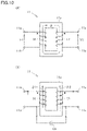
- FIG. 10 is a view illustrating the configuration and operation of sub-insulating transformer 11.
- FIG. 10(A) illustrates the normal transformation operation
- FIG. 10(B) illustrates the operation when the current flows through interphase capacitance C5.
- each of sub-windings 14, 17 is wound around an annular iron core 11e.
- Sub-windings 14, 17 share a magnetic flux ⁇ passing through iron core 11e.
- n1, n2 the numbers of turns of sub-windings 14, 17
- VI the voltages between the terminals of sub-windings 14, 17
- n1 n2.
- V1 and V2 have the same polarity, and have the same phase and the same amplitude.
- FIG. 10(B) when a current I flows from first sub-terminal 11a to third sub-terminal 11c through first sub-winding 14, interphase capacitance C5, and second sub-winding 17, a magnetic flux ⁇ 1 is generated in iron core 11e by current I flowing through first sub-winding 14, and a magnetic flux ⁇ 2 is generated in iron core 11e by current I flowing through second sub-winding 17.
- magnetic flux ⁇ 1 and magnetic flux ⁇ 2 are generated in opposite directions, and magnetic flux ⁇ 1 and magnetic flux ⁇ 2 cancel each other.
- insulating transformer 3 is configured by connecting the plurality of sub-insulating transformers 11 to 13 in series, so that the increase in volume and the weight concentration can be prevented in insulating transformer 3, the assemblability can be improved by enabling the substrate mounting, the heat dissipation can be improved by dispersing the heat source, and the cost reduction can be implemented using the general-purpose sub-insulating transformer with the large distribution amount and easy availability.
- sub-windings 14 to 19 of sub-insulating transformer 11 to 13 are the same, for example, when current I flows from first main terminal 3a to third main terminal 3b through first sub-winding 14, interphase capacitance C5, and second sub-winding 17, the sum of the excitation inductances La, Lb of first and second sub-windings 14, 17 becomes zero. Accordingly, the generation of the resonance phenomenon can be prevented.
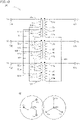
- First sub-insulating transformer 51 includes an iron core (not illustrated), first to third sub-windings 54, 57, 60 wound around the iron core, and first to sixth sub-terminals 51a to 51f.
- a black circle (•) is printed on the positive polarity side of each of first to third sub-windings 54, 57, 60.
- the positive electrode terminal and the negative electrode terminal of first sub-winding 54 are connected to first and second sub-terminals 51a, 51b, respectively.
- the positive electrode terminal and the negative electrode terminal of second sub-winding 57 are connected to third and fourth sub-terminals 51c, 51d, respectively.
- the positive electrode terminal and the negative electrode terminal of third sub-winding 60 are connected to fifth and sixth sub-terminals 51e, 51f, respectively.
- FIG. 12(A) illustrates the case where all the polarity directions of first to third sub-windings 54, 57, 60 are the upward direction.
- a ratio of the numbers of turns of first to third sub-windings 54, 57, 60 is 2:1:1.
- the phases of three-phase AC voltages Vu, Vv, Vw are shifted by 120 degrees, and the phases of three-phase AC voltages Va, Vb, Vc are also shifted by 120 degrees.
- the phases of three-phase AC voltages Va, Vb, Vc are advanced by 30 degrees from the phases of three-phase AC voltages Vu, Vv, Vw, respectively.
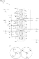
- FIG. 13 is a view illustrating an insulating transformer 65 according to a comparative example of the third exemplary embodiment, and is a view compared with FIG. 12 .
- FIG. 13(A) illustrates the configuration of insulating transformer 65
- FIG. 13(B) illustrates the operation of insulating transformer 65.
- Insulating transformer 65 is different from insulating transformer 50 of FIG. 12 in that first sub-terminals 51a, 52a, 53a of sub-insulating transformers 51, 52, 53 are connected to first neutral point M1, and second sub-terminals 51b, 52b, 53b of sub-insulating transformers 51, 52, 53 are connected to first to third main terminals T21, T22, T23.
- the phases of three-phase AC voltages Vw, Vv, Vu are shifted by 120 degrees, and the phases of three-phase AC voltages Vc, Vb, Va are also shifted by 120 degrees.
- the phases of three-phase AC voltages Vb, Vc, Va are delayed by 30 degrees from the phases of three-phase AC voltages Vu, Vv, Vw, respectively.
- the excitation inductances of sub-windings 60, 57 have the same polarity, and the sum of the excitation inductances of sub-windings 60, 57 has the large value.
- the resonance phenomenon is generated among the interphase capacitance between sub-windings 54, 60, the excitation inductance of sub-winding 60, the interphase capacitance between sub-windings 60, 57, and the excitation inductance of sub-winding 57, and the large voltage vibration is generated. Accordingly, in insulating transformer 65 of the comparative example, the generation of the resonance phenomenon cannot be prevented.
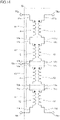
- FIG. 14 is a circuit diagram illustrating a configuration of an insulating transformer 70 according to the fourth embodiment, and is a view compared with FIG. 2 .
- Insulating transformer 70 is different from insulating transformer 3 of FIG. 2 in that first to fourth main terminals 3a to 3d are replaced with first to fifth main terminals 70a to 70e, and that a fourth sub-insulating transformer 71 is added.
- Fourth sub-insulating transformer 71 includes an iron core (not illustrated), first and second sub-windings 72, 73 wound around the iron core, and first to fourth sub-terminals 71a to 71d.
- a black circle (•) is marked on the positive polarity side of each of first and second sub-windings 72, 73.
- the positive electrode terminal and the negative electrode terminal of first sub-winding 72 are connected to first and second sub-terminals 71a, 71b, respectively.
- the positive electrode terminal and the negative electrode terminal of second sub-winding 73 are connected to third and fourth sub-terminals 71c, 71d, respectively.
- FIG. 14 illustrates the case where the polarity direction of first and second sub-windings 72, 73 is the upward direction.
- the numbers of turns of first and second sub-windings 72, 73 are the same.
- First and third sub-terminals 71a, 71c of fourth sub-insulating transformer 71 are connected to second and fourth sub-terminals 13c, 13d of third sub-insulating transformer 13, respectively.
- Second and fourth sub-terminals 71b, 71d of fourth sub-insulating transformer 71 are connected to third and fifth main terminals 70c, 70e, respectively.
- First and third sub-terminals 11a, 11c of first sub-insulating transformer 11 are connected to first and fourth main terminals 70a, 70d, respectively.
- Second main terminal 70b is connected to second sub-terminal 12b of second sub-insulating transformer 12.
- the polarities of eight sub-windings 11 to 13, 17 to 19, 72, 73 are oriented in the same direction.
- Sub-windings 11, 12 configure the first main winding
- sub-windings 13, 72 configure the second main winding
- sub-windings 17 to 19, 73 configure the third main winding.
- the polarities of the first to third main windings are oriented in the same direction.
Landscapes
- Engineering & Computer Science (AREA)
- Power Engineering (AREA)
- Physics & Mathematics (AREA)
- Electromagnetism (AREA)
- Dc-Dc Converters (AREA)
- Rectifiers (AREA)
Applications Claiming Priority (1)
| Application Number | Priority Date | Filing Date | Title |
|---|---|---|---|
| PCT/JP2019/047679 WO2021111601A1 (ja) | 2019-12-05 | 2019-12-05 | 絶縁トランスおよびそれを備えた電力変換装置 |
Publications (2)
| Publication Number | Publication Date |
|---|---|
| EP4071992A1 true EP4071992A1 (de) | 2022-10-12 |
| EP4071992A4 EP4071992A4 (de) | 2023-01-25 |
Family
ID=74845252
Family Applications (1)
| Application Number | Title | Priority Date | Filing Date |
|---|---|---|---|
| EP19954762.1A Pending EP4071992A4 (de) | 2019-12-05 | 2019-12-05 | Isoliertransformator und damit ausgerüstete leistungswandlervorrichtung |
Country Status (5)
| Country | Link |
|---|---|
| US (1) | US12170487B2 (de) |
| EP (1) | EP4071992A4 (de) |
| JP (1) | JP6840296B1 (de) |
| CN (1) | CN114762234B (de) |
| WO (1) | WO2021111601A1 (de) |
Families Citing this family (1)
| Publication number | Priority date | Publication date | Assignee | Title |
|---|---|---|---|---|
| CN113241952A (zh) * | 2021-06-25 | 2021-08-10 | 阳光电源股份有限公司 | 一种隔离式双向变换器及其控制方法 |
Family Cites Families (39)
| Publication number | Priority date | Publication date | Assignee | Title |
|---|---|---|---|---|
| US2428586A (en) * | 1943-07-20 | 1947-10-07 | Westinghouse Electric Corp | Vapor-electric device |
| US3210648A (en) * | 1962-07-09 | 1965-10-05 | Westinghouse Electric Corp | Regulating and current limiting transformer system |
| US3210704A (en) * | 1962-12-27 | 1965-10-05 | Westinghouse Electric Corp | Electrical inductive apparatus having interleaved windings |
| US3745440A (en) * | 1972-02-28 | 1973-07-10 | Litton Systems Inc | Electrical inverter-rectifier circuit and inductor apparatus therefor |
| US4912372A (en) * | 1988-11-28 | 1990-03-27 | Multi Electric Mfg. Co. | Power circuit for series connected loads |
| US5422765A (en) * | 1989-01-24 | 1995-06-06 | Fanuc Ltd. | Inverter device attenuating in-phase harmonic components of an oscillating output signal |
| JPH0365053A (ja) | 1989-04-04 | 1991-03-20 | Hitachi Metals Ltd | スイッチング電源 |
| US5598327A (en) * | 1990-11-30 | 1997-01-28 | Burr-Brown Corporation | Planar transformer assembly including non-overlapping primary and secondary windings surrounding a common magnetic flux path area |
| JPH05268767A (ja) | 1992-03-17 | 1993-10-15 | Toyota Autom Loom Works Ltd | プッシュプルdc−dcコンバータ |
| JP2606997Y2 (ja) | 1993-09-28 | 2001-02-19 | デンセイ・ラムダ株式会社 | スイッチング電源装置 |
| JPH08168249A (ja) * | 1994-10-11 | 1996-06-25 | Sony Corp | 電流共振形スイッチング電源回路 |
| US5754413A (en) * | 1996-02-23 | 1998-05-19 | Lucent Technologies Inc. | Reduced voltage stress asymmetrical DC-to-DC converter using first and second transformers having differing turns ratios |
| US6888709B2 (en) * | 2002-05-03 | 2005-05-03 | Applied Energy Llc | Electromagnetic transient voltage surge suppression system |
| US7573000B2 (en) * | 2003-07-11 | 2009-08-11 | Lincoln Global, Inc. | Power source for plasma device |
| EP1671521B1 (de) * | 2003-10-06 | 2010-02-17 | Microsemi Corporation | Stromteilungsschema und einrichtung für mehrfach-ccf-lampenbetrieb |
| JP2008140547A (ja) * | 2004-10-28 | 2008-06-19 | Minebea Co Ltd | 多灯式放電灯点灯装置 |
| US7932693B2 (en) * | 2005-07-07 | 2011-04-26 | Eaton Corporation | System and method of controlling power to a non-motor load |
| WO2007143605A2 (en) * | 2006-06-05 | 2007-12-13 | Daniel Princinsky | Electromagnetic noise suppression system for wye power distribution |
| JP5030157B2 (ja) * | 2007-11-15 | 2012-09-19 | コーセル株式会社 | スイッチング電源装置 |
| EP2416486B1 (de) * | 2009-03-30 | 2018-05-30 | Hitachi, Ltd. | Leistungswandler |
| CN103329420B (zh) * | 2011-01-26 | 2015-12-02 | 株式会社村田制作所 | 开关电源电路 |
| WO2012101905A1 (ja) * | 2011-01-26 | 2012-08-02 | 株式会社村田製作所 | スイッチング電源装置 |
| JP5824862B2 (ja) * | 2011-05-11 | 2015-12-02 | 株式会社リコー | 高電圧インバータ装置 |
| CN103595367B (zh) * | 2013-11-07 | 2017-03-08 | 华为技术有限公司 | 一种磁集成器件及一种功率转换电路 |
| JP2015142419A (ja) * | 2014-01-28 | 2015-08-03 | 新電元工業株式会社 | 複合トランス及び共振コンバータ |
| US10707747B2 (en) * | 2015-07-21 | 2020-07-07 | Christopher Donovan Davidson | Single stage isolated AC/DC power factor corrected converter |
| US9874897B2 (en) * | 2016-05-03 | 2018-01-23 | Toyota Motor Engineering & Manufacturing North America, Inc. | Integrated inductor |
| DE112017003632T5 (de) | 2016-07-19 | 2019-04-11 | Mitsubishi Electric Corporation | Dc/dc-umrichter |
| US20190348213A1 (en) * | 2017-04-17 | 2019-11-14 | Mitsubishi Electric Corporation | Planar transformer, laser diode-driving power supply, and laser machining apparatus |
| US10672553B2 (en) * | 2017-05-10 | 2020-06-02 | Raytheon Company | High voltage high frequency transformer |
| JP6461439B1 (ja) * | 2017-08-23 | 2019-01-30 | 三菱電機株式会社 | Dc/dcコンバータ |
| KR102211454B1 (ko) * | 2017-08-31 | 2021-02-04 | 한국전자기술연구원 | 절연형 dc-dc 컨버터 및 그 구동방법 |
| JP6939410B2 (ja) * | 2017-10-26 | 2021-09-22 | 富士電機株式会社 | トランス |
| JP2019169690A (ja) * | 2018-03-26 | 2019-10-03 | 田淵電機株式会社 | トランス及びこれを用いたllc共振回路 |
| FR3084796B1 (fr) * | 2018-07-31 | 2020-08-28 | Valeo Siemens Eautomotive Norway As | Convertisseur de tension continu-continu a resonance |
| US10742123B1 (en) * | 2019-03-05 | 2020-08-11 | Astec International Limited | Low common mode noise transformers and switch-mode DC-DC power converters |
| WO2021106941A1 (ja) * | 2019-11-25 | 2021-06-03 | アイシン・エィ・ダブリュ株式会社 | 制御基板 |
| KR20230009661A (ko) * | 2021-07-09 | 2023-01-17 | 현대자동차주식회사 | 차량용 양방향 충전 시스템 |
| US11777487B1 (en) * | 2022-04-07 | 2023-10-03 | GE Precision Healthcare LLC | Gate driver coreless transformers for magnetic resonance imaging power electronics |
-
2019
- 2019-12-05 EP EP19954762.1A patent/EP4071992A4/de active Pending
- 2019-12-05 JP JP2020540509A patent/JP6840296B1/ja active Active
- 2019-12-05 WO PCT/JP2019/047679 patent/WO2021111601A1/ja not_active Ceased
- 2019-12-05 CN CN201980102645.7A patent/CN114762234B/zh active Active
- 2019-12-05 US US17/766,534 patent/US12170487B2/en active Active
Also Published As
| Publication number | Publication date |
|---|---|
| CN114762234A (zh) | 2022-07-15 |
| EP4071992A4 (de) | 2023-01-25 |
| JPWO2021111601A1 (ja) | 2021-12-02 |
| CN114762234B (zh) | 2025-11-14 |
| JP6840296B1 (ja) | 2021-03-10 |
| WO2021111601A1 (ja) | 2021-06-10 |
| US12170487B2 (en) | 2024-12-17 |
| US20230208304A1 (en) | 2023-06-29 |
Similar Documents
| Publication | Publication Date | Title |
|---|---|---|
| CN102301576B (zh) | 直流/直流转换器和交流/直流转换器 | |
| US8508957B2 (en) | Power conversion device for converting DC power to AC power | |
| EP3059847B1 (de) | Stromwandlervorrichtung und stromumwandlungsverfahren | |
| EP2784925B1 (de) | Stromwandler | |
| EP3528373B1 (de) | Leistungswandlungssystem | |
| US20110316461A1 (en) | Open Delta Motor Drive With Integrated Recharge | |
| US6831442B2 (en) | Utilizing zero-sequence switchings for reversible converters | |
| US8922151B2 (en) | Regenerative medium voltage inverter | |
| US11909305B2 (en) | AC-to-DC power converter which removed a common mode component form the output current | |
| JP7008222B2 (ja) | 電力変換システム | |
| US11990830B2 (en) | Power conversion system and virtual DC voltage generator circuit | |
| US20240332979A1 (en) | Power conversion system including a second circuit being configured to control a current or power such that the current or the power is synchronized with power ripples caused by the ac power supply or the ac load | |
| US10027239B2 (en) | Wind power converter device and converter device | |
| CN114762234B (zh) | 绝缘变压器以及具备其的电力变换装置 | |
| JP2007300712A (ja) | 交流電力供給装置 | |
| Li et al. | Asymmetrical modular multilevel converter with sensorless voltage control for high-quality output | |
| US20090034305A1 (en) | Power Conversion Device and Power Conversion System | |
| US12609636B2 (en) | Power conversion device | |
| EP1589648A2 (de) | Dreiphasen Gleichstrom/Gleichstrom-Wandler | |
| US20240195340A1 (en) | Power supply system supplying an electrical load via a polyphase voltage and an auxiliary network via a homopolar component of the voltage, and related electrical installation | |
| JPWO2013136428A1 (ja) | リアクトルおよびそれを用いた電源装置 | |
| KR101862517B1 (ko) | 독립형 멀티 h-브리지를 이용한 다상 인버터 | |
| CN108574422B (zh) | 电源转换器与电源转换方法 | |
| CN101199108A (zh) | 用于将dc电压转换为三相ac输出的方法和变换器 | |
| JP2023044947A (ja) | 電力変換装置 |
Legal Events
| Date | Code | Title | Description |
|---|---|---|---|
| STAA | Information on the status of an ep patent application or granted ep patent |
Free format text: STATUS: THE INTERNATIONAL PUBLICATION HAS BEEN MADE |
|
| PUAI | Public reference made under article 153(3) epc to a published international application that has entered the european phase |
Free format text: ORIGINAL CODE: 0009012 |
|
| STAA | Information on the status of an ep patent application or granted ep patent |
Free format text: STATUS: REQUEST FOR EXAMINATION WAS MADE |
|
| 17P | Request for examination filed |
Effective date: 20220531 |
|
| AK | Designated contracting states |
Kind code of ref document: A1 Designated state(s): AL AT BE BG CH CY CZ DE DK EE ES FI FR GB GR HR HU IE IS IT LI LT LU LV MC MK MT NL NO PL PT RO RS SE SI SK SM TR |
|
| A4 | Supplementary search report drawn up and despatched |
Effective date: 20230103 |
|
| RIC1 | Information provided on ipc code assigned before grant |
Ipc: H02M 3/28 20060101AFI20221221BHEP |
|
| DAV | Request for validation of the european patent (deleted) | ||
| DAX | Request for extension of the european patent (deleted) |