EP4080253A1 - Sandwichstruktur und verfahren zur herstellung davon - Google Patents
Sandwichstruktur und verfahren zur herstellung davon Download PDFInfo
- Publication number
- EP4080253A1 EP4080253A1 EP20902491.8A EP20902491A EP4080253A1 EP 4080253 A1 EP4080253 A1 EP 4080253A1 EP 20902491 A EP20902491 A EP 20902491A EP 4080253 A1 EP4080253 A1 EP 4080253A1
- Authority
- EP
- European Patent Office
- Prior art keywords
- surface portion
- metal oxide
- substrate
- depth
- holes
- Prior art date
- Legal status (The legal status is an assumption and is not a legal conclusion. Google has not performed a legal analysis and makes no representation as to the accuracy of the status listed.)
- Granted
Links
Images




Classifications
-
- C—CHEMISTRY; METALLURGY
- C03—GLASS; MINERAL OR SLAG WOOL
- C03C—CHEMICAL COMPOSITION OF GLASSES, GLAZES OR VITREOUS ENAMELS; SURFACE TREATMENT OF GLASS; SURFACE TREATMENT OF FIBRES OR FILAMENTS MADE FROM GLASS, MINERALS OR SLAGS; JOINING GLASS TO GLASS OR OTHER MATERIALS
- C03C17/00—Surface treatment of glass, not in the form of fibres or filaments, by coating
- C03C17/22—Surface treatment of glass, not in the form of fibres or filaments, by coating with other inorganic material
- C03C17/23—Oxides
- C03C17/245—Oxides by deposition from the vapour phase
-
- G—PHYSICS
- G02—OPTICS
- G02B—OPTICAL ELEMENTS, SYSTEMS OR APPARATUS
- G02B1/00—Optical elements characterised by the material of which they are made; Optical coatings for optical elements
- G02B1/10—Optical coatings produced by application to, or surface treatment of, optical elements
- G02B1/11—Anti-reflection coatings
- G02B1/118—Anti-reflection coatings having sub-optical wavelength surface structures designed to provide an enhanced transmittance, e.g. moth-eye structures
-
- C—CHEMISTRY; METALLURGY
- C03—GLASS; MINERAL OR SLAG WOOL
- C03C—CHEMICAL COMPOSITION OF GLASSES, GLAZES OR VITREOUS ENAMELS; SURFACE TREATMENT OF GLASS; SURFACE TREATMENT OF FIBRES OR FILAMENTS MADE FROM GLASS, MINERALS OR SLAGS; JOINING GLASS TO GLASS OR OTHER MATERIALS
- C03C17/00—Surface treatment of glass, not in the form of fibres or filaments, by coating
- C03C17/22—Surface treatment of glass, not in the form of fibres or filaments, by coating with other inorganic material
- C03C17/23—Oxides
- C03C17/245—Oxides by deposition from the vapour phase
- C03C17/2456—Coating containing TiO2
-
- C—CHEMISTRY; METALLURGY
- C23—COATING METALLIC MATERIAL; COATING MATERIAL WITH METALLIC MATERIAL; CHEMICAL SURFACE TREATMENT; DIFFUSION TREATMENT OF METALLIC MATERIAL; COATING BY VACUUM EVAPORATION, BY SPUTTERING, BY ION IMPLANTATION OR BY CHEMICAL VAPOUR DEPOSITION, IN GENERAL; INHIBITING CORROSION OF METALLIC MATERIAL OR INCRUSTATION IN GENERAL
- C23C—COATING METALLIC MATERIAL; COATING MATERIAL WITH METALLIC MATERIAL; SURFACE TREATMENT OF METALLIC MATERIAL BY DIFFUSION INTO THE SURFACE, BY CHEMICAL CONVERSION OR SUBSTITUTION; COATING BY VACUUM EVAPORATION, BY SPUTTERING, BY ION IMPLANTATION OR BY CHEMICAL VAPOUR DEPOSITION, IN GENERAL
- C23C14/00—Coating by vacuum evaporation, by sputtering or by ion implantation of the coating forming material
- C23C14/06—Coating by vacuum evaporation, by sputtering or by ion implantation of the coating forming material characterised by the coating material
- C23C14/10—Glass or silica
-
- C—CHEMISTRY; METALLURGY
- C23—COATING METALLIC MATERIAL; COATING MATERIAL WITH METALLIC MATERIAL; CHEMICAL SURFACE TREATMENT; DIFFUSION TREATMENT OF METALLIC MATERIAL; COATING BY VACUUM EVAPORATION, BY SPUTTERING, BY ION IMPLANTATION OR BY CHEMICAL VAPOUR DEPOSITION, IN GENERAL; INHIBITING CORROSION OF METALLIC MATERIAL OR INCRUSTATION IN GENERAL
- C23C—COATING METALLIC MATERIAL; COATING MATERIAL WITH METALLIC MATERIAL; SURFACE TREATMENT OF METALLIC MATERIAL BY DIFFUSION INTO THE SURFACE, BY CHEMICAL CONVERSION OR SUBSTITUTION; COATING BY VACUUM EVAPORATION, BY SPUTTERING, BY ION IMPLANTATION OR BY CHEMICAL VAPOUR DEPOSITION, IN GENERAL
- C23C14/00—Coating by vacuum evaporation, by sputtering or by ion implantation of the coating forming material
- C23C14/22—Coating by vacuum evaporation, by sputtering or by ion implantation of the coating forming material characterised by the process of coating
- C23C14/34—Sputtering
-
- C—CHEMISTRY; METALLURGY
- C03—GLASS; MINERAL OR SLAG WOOL
- C03C—CHEMICAL COMPOSITION OF GLASSES, GLAZES OR VITREOUS ENAMELS; SURFACE TREATMENT OF GLASS; SURFACE TREATMENT OF FIBRES OR FILAMENTS MADE FROM GLASS, MINERALS OR SLAGS; JOINING GLASS TO GLASS OR OTHER MATERIALS
- C03C2217/00—Coatings on glass
- C03C2217/20—Materials for coating a single layer on glass
- C03C2217/21—Oxides
- C03C2217/211—SnO2
-
- C—CHEMISTRY; METALLURGY
- C03—GLASS; MINERAL OR SLAG WOOL
- C03C—CHEMICAL COMPOSITION OF GLASSES, GLAZES OR VITREOUS ENAMELS; SURFACE TREATMENT OF GLASS; SURFACE TREATMENT OF FIBRES OR FILAMENTS MADE FROM GLASS, MINERALS OR SLAGS; JOINING GLASS TO GLASS OR OTHER MATERIALS
- C03C2217/00—Coatings on glass
- C03C2217/20—Materials for coating a single layer on glass
- C03C2217/21—Oxides
- C03C2217/212—TiO2
-
- C—CHEMISTRY; METALLURGY
- C03—GLASS; MINERAL OR SLAG WOOL
- C03C—CHEMICAL COMPOSITION OF GLASSES, GLAZES OR VITREOUS ENAMELS; SURFACE TREATMENT OF GLASS; SURFACE TREATMENT OF FIBRES OR FILAMENTS MADE FROM GLASS, MINERALS OR SLAGS; JOINING GLASS TO GLASS OR OTHER MATERIALS
- C03C2217/00—Coatings on glass
- C03C2217/20—Materials for coating a single layer on glass
- C03C2217/21—Oxides
- C03C2217/213—SiO2
-
- C—CHEMISTRY; METALLURGY
- C03—GLASS; MINERAL OR SLAG WOOL
- C03C—CHEMICAL COMPOSITION OF GLASSES, GLAZES OR VITREOUS ENAMELS; SURFACE TREATMENT OF GLASS; SURFACE TREATMENT OF FIBRES OR FILAMENTS MADE FROM GLASS, MINERALS OR SLAGS; JOINING GLASS TO GLASS OR OTHER MATERIALS
- C03C2217/00—Coatings on glass
- C03C2217/20—Materials for coating a single layer on glass
- C03C2217/21—Oxides
- C03C2217/216—ZnO
-
- C—CHEMISTRY; METALLURGY
- C03—GLASS; MINERAL OR SLAG WOOL
- C03C—CHEMICAL COMPOSITION OF GLASSES, GLAZES OR VITREOUS ENAMELS; SURFACE TREATMENT OF GLASS; SURFACE TREATMENT OF FIBRES OR FILAMENTS MADE FROM GLASS, MINERALS OR SLAGS; JOINING GLASS TO GLASS OR OTHER MATERIALS
- C03C2217/00—Coatings on glass
- C03C2217/20—Materials for coating a single layer on glass
- C03C2217/21—Oxides
- C03C2217/218—V2O5, Nb2O5, Ta2O5
-
- C—CHEMISTRY; METALLURGY
- C03—GLASS; MINERAL OR SLAG WOOL
- C03C—CHEMICAL COMPOSITION OF GLASSES, GLAZES OR VITREOUS ENAMELS; SURFACE TREATMENT OF GLASS; SURFACE TREATMENT OF FIBRES OR FILAMENTS MADE FROM GLASS, MINERALS OR SLAGS; JOINING GLASS TO GLASS OR OTHER MATERIALS
- C03C2217/00—Coatings on glass
- C03C2217/20—Materials for coating a single layer on glass
- C03C2217/21—Oxides
- C03C2217/22—ZrO2
-
- C—CHEMISTRY; METALLURGY
- C03—GLASS; MINERAL OR SLAG WOOL
- C03C—CHEMICAL COMPOSITION OF GLASSES, GLAZES OR VITREOUS ENAMELS; SURFACE TREATMENT OF GLASS; SURFACE TREATMENT OF FIBRES OR FILAMENTS MADE FROM GLASS, MINERALS OR SLAGS; JOINING GLASS TO GLASS OR OTHER MATERIALS
- C03C2217/00—Coatings on glass
- C03C2217/20—Materials for coating a single layer on glass
- C03C2217/21—Oxides
- C03C2217/228—Other specific oxides
-
- C—CHEMISTRY; METALLURGY
- C03—GLASS; MINERAL OR SLAG WOOL
- C03C—CHEMICAL COMPOSITION OF GLASSES, GLAZES OR VITREOUS ENAMELS; SURFACE TREATMENT OF GLASS; SURFACE TREATMENT OF FIBRES OR FILAMENTS MADE FROM GLASS, MINERALS OR SLAGS; JOINING GLASS TO GLASS OR OTHER MATERIALS
- C03C2217/00—Coatings on glass
- C03C2217/20—Materials for coating a single layer on glass
- C03C2217/25—Metals
- C03C2217/27—Mixtures of metals, alloys
-
- C—CHEMISTRY; METALLURGY
- C03—GLASS; MINERAL OR SLAG WOOL
- C03C—CHEMICAL COMPOSITION OF GLASSES, GLAZES OR VITREOUS ENAMELS; SURFACE TREATMENT OF GLASS; SURFACE TREATMENT OF FIBRES OR FILAMENTS MADE FROM GLASS, MINERALS OR SLAGS; JOINING GLASS TO GLASS OR OTHER MATERIALS
- C03C2217/00—Coatings on glass
- C03C2217/70—Properties of coatings
- C03C2217/73—Anti-reflective coatings with specific characteristics
-
- C—CHEMISTRY; METALLURGY
- C03—GLASS; MINERAL OR SLAG WOOL
- C03C—CHEMICAL COMPOSITION OF GLASSES, GLAZES OR VITREOUS ENAMELS; SURFACE TREATMENT OF GLASS; SURFACE TREATMENT OF FIBRES OR FILAMENTS MADE FROM GLASS, MINERALS OR SLAGS; JOINING GLASS TO GLASS OR OTHER MATERIALS
- C03C2217/00—Coatings on glass
- C03C2217/70—Properties of coatings
- C03C2217/73—Anti-reflective coatings with specific characteristics
- C03C2217/732—Anti-reflective coatings with specific characteristics made of a single layer
-
- C—CHEMISTRY; METALLURGY
- C03—GLASS; MINERAL OR SLAG WOOL
- C03C—CHEMICAL COMPOSITION OF GLASSES, GLAZES OR VITREOUS ENAMELS; SURFACE TREATMENT OF GLASS; SURFACE TREATMENT OF FIBRES OR FILAMENTS MADE FROM GLASS, MINERALS OR SLAGS; JOINING GLASS TO GLASS OR OTHER MATERIALS
- C03C2218/00—Methods for coating glass
- C03C2218/10—Deposition methods
- C03C2218/15—Deposition methods from the vapour phase
- C03C2218/154—Deposition methods from the vapour phase by sputtering
-
- C—CHEMISTRY; METALLURGY
- C03—GLASS; MINERAL OR SLAG WOOL
- C03C—CHEMICAL COMPOSITION OF GLASSES, GLAZES OR VITREOUS ENAMELS; SURFACE TREATMENT OF GLASS; SURFACE TREATMENT OF FIBRES OR FILAMENTS MADE FROM GLASS, MINERALS OR SLAGS; JOINING GLASS TO GLASS OR OTHER MATERIALS
- C03C2218/00—Methods for coating glass
- C03C2218/10—Deposition methods
- C03C2218/15—Deposition methods from the vapour phase
- C03C2218/154—Deposition methods from the vapour phase by sputtering
- C03C2218/156—Deposition methods from the vapour phase by sputtering by magnetron sputtering
-
- G—PHYSICS
- G02—OPTICS
- G02B—OPTICAL ELEMENTS, SYSTEMS OR APPARATUS
- G02B2207/00—Coding scheme for general features or characteristics of optical elements and systems of subclass G02B, but not including elements and systems which would be classified in G02B6/00 and subgroups
- G02B2207/101—Nanooptics
Definitions
- the present invention relates to an antireflection structure having functions such as an optical antireflection function, a hydrophilic function and the like, and to a manufacturing method thereof.
- JP 2019-227726 The contents of the Japanese patent application ( JP 2019-227726) filed on December 17, 2019 , which is the basis of the present application, are incorporated by reference herein as part of this specification.
- a surface treatment is performed in order to reduce return light due to surface reflection and to increase transmitted light.
- a specific method of this surface treatment a method of periodically forming fine and dense uneven shapes on the surface portion of an optical element is known. In this way, when a periodic concave-convex shape is provided on the surface portion of the optical element, light is diffracted as it passes through the optical element surface, and the straight component of the transmitted light is greatly reduced.
- the pitch of the concave-convex shape formed on the surface portion of the optical element is shorter than the wavelength of the transmitted light, it is possible to obtain an effective antireflection effect for the light having a wavelength corresponding to the pitch, the depth, and the like because the light does not diffract.
- nanostructure a nanometer-sized concave-convex structure
- Such structures can be manufactured by processing methods such as etching using semiconductor processes or aluminum anodization.
- the concavo-convex pattern spacing of the nanostructure can be kept below the wavelength, and the height (or depth) of its concave-convex shape (denoting the wavelength by ⁇ and the refractive index of the structure by n) can be controlled to be about ⁇ /4n to ⁇ /2n of the wavelength, and can be molded at low cost by transfer molding (see Patent Document 3 and Patent Document 4).
- the wavelength to prevent reflection is determined by the depth of the concave-convex shape of the structure, so the depth of the concave-convex shape needs to be controlled.
- the specified concave-convex structure is formed by using an etching process to process the concave-convex surface, or by transfer molding using a mold.
- the antireflection properties of the nanostructures are determined by the depth of the concave shape of the structure, making it difficult to produce molded products with uniform antireflection properties and low reflection.
- the purpose of this invention is to provide antireflection structures with excellent in-plane uniformity of optical properties and excellent antireflection optical properties for a wide wavelength band and a wider angle of incidence, by forming thicker columnar films in the deeper recessed portions to reduce the depth variation from the uppermost surface portion of the structure to the surface portion of the columnar film in the concave portion, and to provide a manufacturing method thereof.
- the present inventors have focused on the point that the collision between the thin-film forming particles and inert gas particles is enhanced and the mean free path of these particles becomes shorter by setting the pressure in the vacuum chamber to a lower level than that normally used in the vacuum deposition method (i.e., the pressure is set relatively high), when a thin film or the like is formed by a vacuum film deposition on a surface portion and inside the holes of a nanostructure in which a plurality of holes, that have hole diameters of nanometer size less than the wavelength of the light to be prevented from being reflected and that have an average distance between the center points of the openings less than the wavelength of the light, are formed on a surface portion of a flat transparent substrate.
- the gist of the preset invention is the invention summarized in the following (1) to (17).
- the antireflection structure of the present invention since metal oxides having an antireflection function are formed, as a thin film and as columnar films, on the surface portion (S) of the substrate (B) and in the space portions (Cn) from the bottom to the top of a plurality of nanometer-sized holes (Hn) having a depth (dn) and provided in the surface portion (S), respectively, the antireflection structure has an excellent antireflection effect and hydrophilic properties.
- each columnar film placed in the space portion (Cn) of each hole (Hn) is arranged to be increased as the depth (dn) of each hole (Hn) in the substrate (B) becomes larger, differences in depth (fn) between the respective holes (Hn) from the uppermost surface portion (Sm) of the substrate (B) decrease and, as a result, the antireflection structure exhibits a remarkable antireflection effect.
- the antireflection structure of the present invention by performing vacuum deposition on the substrate (B) provided with multiple nanometer-sized holes (Hn) under specific conditions using a vacuum film deposition apparatus having a plasma source, the surface portion (S) thereof and the space portion (Cn) in the upper direction from the bottom of each hole (Hn) are deposited, with a thin film and columnar films consisting of metal oxides (M) with antireflection functions respectively, and, as a result, the antireflection structure has excellent antireflection effects and hydrophilic properties.
- the thickness (tn) of each columnar film deposited in the space portion (Cn) of each hole (Hn) increases as the depth (dn) before deposition of each hole (Hn) in the substrate (B) becomes larger, so that differences in depth (fn) between the respective holes (Hn) from the uppermost surface portion (Sm) of the substrate (B) decrease, and as a result, the obtained antireflection structure exhibits a remarkable antireflection effect.
- metal oxide M
- metal oxide metal oxide
- the present invention will be described below as [1] the antireflection structure and [2] the method for manufacturing an antireflection structure, separately.
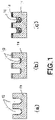
- 1(a) is the conceptual view of the substrate (B) 11 with holes 12 having a U-shaped cross-sectional shape in a direction perpendicular to the surface portion
- 1(b) is the conceptual view of a structure in which the thin film 13 is placed on the surface portion and holes of the substrate (B) 11 by a known method
- 1(c) is the conceptual diagram of the antireflection structure in which the thin film 14 made of metal oxide is disposed on the surface portion (S) of the substrate (B) 11, and the columnar film 15 made of metal oxide is disposed in the space portion (Cn) of each hole (Hn) 12.
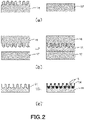
- FIGs. 2(a) to 2(c) are conceptual diagrams showing the process of manufacturing the substrate (B) and the process of manufacturing the antireflection structure from the substrate (B).
- 2(a) is the conceptual diagram of the upper mold 16 and the lower mold 17 for injection molding
- 2(b) is the conceptual diagram of the injection molding process in which molten resin to form the substrate (B) 11 is injected into the space where these molds are set in the injection molding machine
- 2(c) is the conceptual diagram of the process of depositing the thin film 14 on the surface portion (S) of the substrate (B) 11 formed by the above injection molding process and depositing the columnar film 15 in the space portion (Cn) of each hole (Hn) formed in the substrate (B) by the vacuum film deposition process of this invention.
- FIGs. 3 (a) to (c) are the SEM images of the specimen (A-2), specimen (B-2), and specimen (C-5) obtained in Reference Example 1, Example 1, and Comparative Example 2, respectively, observed from the upper side of the surface.
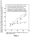
- FIG. 4 shows the measurement results of the depth (fn) of each hole in the specimen (B-2) after deposition obtained by the process of the present invention, and in the specimen (C-5) after deposition obtained by a known process, corresponding to the depth (dn) of each hole (Hn) provided in the specimen (A-2) in Example 3 and Comparative Example 3 herein.
- FIGs. 5 to 7 are diagrams illustrating the optical properties (relationship between the wavelength of incident light and reflectance of incident light) of the specimens (A-2), (B-2), and (C-5) obtained in Reference Example 1, Example 1, and Comparative Example 2 respectively above when an angle of incident light is 5 degrees.
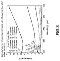
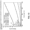
- FIGs. 8 to 10 are diagrams illustrating the optical properties (relationship between the wavelength of incident light and reflectance of incident light) of the specimens (A-2), (B-2), and (C-5) obtained in Reference Example 1, Example 1, and Comparative Example 2 respectively above at each angle of incidence of light within the range of 5 degrees to 70 degrees.
- FIGs. 3 to 10 will be described in examples and comparative examples herein.
- the antireflection structure comprises a transparent substrate (B) having a plurality of holes (Hn) with U-shaped or V-shaped cross-sectional shapes in a direction perpendicular to a flat surface portion thereof, and a metal oxide film disposed on the surface portion (S) of the transparent substrate (B) and in space portions (Cn) formed in an upward direction from bottom portions of the holes (Hn) of the transparent substrate (B),
- the substrate (B) is a transparent structure in which a plurality of holes (Hn), each with a U-shaped or V-shaped cross-sectional shape in a direction perpendicular to the flat surface portion, are formed, and the geometry of each hole (Hn) is such that an average diameter of the openings (m) is 50 nm to 300 nm, an average distance (k) between the center points of openings of adjacent holes (Hn) is 100 nm to 400 nm, and an depth (dn) of each hole (Hn) from the surface portion (S) of the substrate (B) is 80 nm to 250 nm.
- organic material usable for the substrate (B) polycarbonate resin, polyacrylic resin, polyamide resin, polyester resin, polyolefin resin, polycycloolefin resin, polyurethane resin, cellulose resin, polyvinyl chloride resin, polyether resin, polyarylate resin and others can be used, but not limited thereto.
- inorganic material usable for the substrate (B) glass, silicon, quartz, ceramic material and others can be used, but not limited thereto.
- the use of organic materials is preferable in consideration of the processability in forming holes (Hn).
- the polycarbonate is more preferable because of its excellent transparency, impact resistance, heat resistance, dimensional stability and self-digestibility, and polyethylene terephthalate is more preferable because of its excellent heat resistance, mechanical strength, dimensional stability, chemical resistance, optical properties, etc., as well as surface smoothness and handling properties.
- the surface portion of the substrate (B) is flat, and its surface roughness is preferably 50 nm or less in terms of arithmetic mean roughness (Ra) based on JIS 601.
- the flat shape also includes a curved shape with a gentle curvature. There is no restriction on the thickness of the substrate (B).
- each hole (Hn) provided on the surface portion (S) of the substrate (B) is the U-shaped or V-shaped cross-sectional structure in the direction perpendicular to the surface portion, as shown in the conceptual diagram in FIG. 1(a) or the like.
- the average diameter (m) of the opening of each hole (Hn) provided on the surface portion (S) of the substrate (B) is 50 nm to 300 nm, preferably 80 nm to 300 nm, in consideration of the antireflection effect of visible light.
- the average distance (k) between the center points of openings of the adjacent holes (Hn) is 100 nm to 400 nm, preferably 100 nm to 350 nm, from the viewpoint of the antireflection effect of the light.
- the area ratio (r) of the openings (aperture ratio) of the holes (Hn) in the surface portion (S) of the substrate (B) is preferably 50 to 80 area %.
- the depth (dn) of each hole (Hn) from the surface portion (S) of the substrate (B) is 80 nm to 250 nm in consideration of the antireflection function and the placement of the thin film described later, and is preferably 90 nm to 230 nm when the refractive index of the substrate (B) is 1.46.
- the average diameter (m) of the opening of each hole (Hn) and the average distance (k) between the center points of openings of the adjacent holes (Hn) are the median values obtained from the normal distribution of the measured values, and the range of the depth (dn) of each hole (Hn) above should include 70% or more of the measured values if there is some variation.
- the structure of the above substrate (B) can be formed by using an upper mold 16 for injection molding and a lower mold 17 for injection molding shown in FIG. 2(a) , and by adopting a process of injecting the molten resin which forms the substrate (B) into the space in which these molds are set in the injection molding machine shown in FIG. 2 (b) .
- it can be formed by casting, press molding, etc. using the mold composed of nanostructures.
- metal oxide is disposed as the thin film on the surface portion (S) of the transparent substrate (B), and metal oxide is disposed as the columnar film in the space portion (Cn) of each hole (Hn).
- One of the features of the antireflection structure of the present invention is that as shown in FIG. 1(c) , a thin film made of metal oxide is disposed on the surface portion (S) of the structure, and columnar film made of the same metal oxide is disposed in the space portion (Cn) of each hole (Hn), which is in a different structure from the aforementioned thin film, to perform the antireflection function.
- a further feature of the present invention is that a thickness (tn) of the columnar film made of the metal oxide and formed in the space portion (Cn) of each hole (Hn) increases as the depth (dn) of each the holes (Hn) before deposition becomes larger, as described below, so that differences in depth (fn) after deposition between the respective holes (Hn) are reduced, thereby further improving the antireflection function.
- inorganic metal oxides (M) that are placed on the surface portion (S) and in the space portion (Cn) of each hole (Hn) in the substrate (B) and that form metal oxide films capable of performing antireflection effects include silicon oxide, aluminum oxide (alumina), zirconium silicate, rutile-type titanium oxide, tin oxide, zirconium oxide, cerium oxide, zinc oxide, iron oxide, antimony oxide, niobium pentoxide, and copper oxide.
- silicon oxide, aluminum oxide, titanium oxide, and zirconium oxide (zirconia) with a low refractive index are preferred.
- the thickness (p) of the thin film of metal oxide film disposed on the surface portion (S) of the substrate (B) is preferably 20 nm to 60 nm, and 20 nm to 40 nm is more preferable, considering the thickness (tn) of the columnar film disposed in the space portion (Cn) of each hole (Hn) and the antireflection function, etc.
- FIG. 3(b) is a SEM image of the antireflection structure obtained in Example 1 herein, and the prior art and the like.
- FIG. 3 (b) is the SEM image of the antireflection structure obtained in Example 1 herein, and the Thornton model (see International Publication No. 2008-07190 6 , and J. A. Thornton, J Vac. Sci. Technol. 11, p666 1974 ).
- the columnar film is preferably disposed in the direction toward the bottom of the hole (Hn) from a position about 120 nm relative to the uppermost surface portion (Sm) of the thin film-bearing substrate (B) and is more preferably disposed through a depth of 120 to 250nm. Preferred thickness (tn (nm)) of the columnar film is described later.
- the antireflection structure of the present invention is characterized by the thin film made of metal oxide disposed on the surface portion (S) of the transparent substrate (B) provided with a plurality of holes (Hn) of the above specific nanometer size, and the columnar film of the different structure from the above thin film disposed in the space portion (Cn) of each hole (Hn), thereby the antireflection function is performed, and further, since the columnar film is fibrous, the antireflection effect, the hydrophilic effect, and the anti-fog effect are improved.
- the thickness (tn) of the columnar film made of metal oxide formed in the space portions (Cn) of each of the holes (Hn) increases as the depth (dn (nm)) of each hole (Hn) provided in the substrate (B) becomes larger.
- each depth (fn (nm)) from the uppermost surface portion (Sm) of the substrate (B) to the surface portion of the metal oxide film in the space portion (Cn) of each hole (Hn) can be obtained from the following equation (iii), as described later.
- fn 0.195 dn + 95.5
- each columnar film formed in each space portion (Cn) can be obtained from the following equation (iv).
- tn dn + p ⁇ fn
- the thickness (p) of the thin film placed on the surface portion (S) of the substrate (B) can be generalized to a range of 20 nm to 40 nm, and a preferable range of each depth (fn) from the uppermost surface portion (Sm) of the substrate (B) to the surface portions of the columnar film in the space portions (Cn) of the holes (Hn) can be determined.
- the thickness (p) of the thin film disposed on the surface portion (S) of the substrate (B) is 20 nm to 40 nm, preferably 20 nm to 30 nm, and when the depth (dn) of each hole (Hn) of the substrate (B) is 80 nm to 250 nm, the depth (fn (nm)) of each hole (Hn) from the uppermost surface portion (Sm) of the substrate (B) to the surface portion of the metal oxide film disposed in the space portion (Cn) of the hole (Hn) is preferably in the range indicated by the following formula (i), which is calculated from the depth (dn (nm)) of each hole (Hn) before film disposition relative to the surface portion (S).
- fn 0.195 dn + 95.5 + p ⁇ 25 ⁇ 0.90 to 0.195 dn + 95.5 + p ⁇ 25 ⁇ 1.10
- (p - 25) takes into consideration that the thickness (p) of the thin film disposed on the surface portion of the substrate (B) is within the above range, and the coefficients 0.90 and 1.10 are numerical values for indicating the upper limit and the lower limit of the depth (fn) in consideration of the range of variation in FIG. 4 , and the unit of the numeral is a nanometer (nm).
- the effect of the present invention may be suitably performed.
- the thickness (p) of the thin film disposed on the surface portion (S) of the substrate (B) is 20 nm to 40 nm, preferably 20 nm to 30 nm, and when the depth (dn) of each hole (Hn) of the substrate (B) is 80 nm to 250 nm, the depth (fn (nm)) of each hole (Hn) from the uppermost surface portion (Sm) of the substrate (B) to the surface portion of the metal oxide film placed in the space portion (Cn) of each hole (Hn) is more preferably in the range shown in the following formula (ii), which is obtained from the depth (dn (nm)) of each hole (Hn) before deposition relative to the surface portion (S).
- fn 0.195 dn + 95.5 + p ⁇ 25 ⁇ 0.95 to 0.195 dn + 95.5 + p ⁇ 25 ⁇ 1.05
- (p - 25) takes into consideration that the thickness (p) of the thin film disposed on the surface portion of the substrate (B) is within the above range, and the coefficients 0.95 and 1.05 are numerical values for indicating the upper limit and the lower limit of the depth (fn) in consideration of the range of variation in FIG. 4 , and the unit of the numeral is a nanometer (nm).
- the antireflection structure of the present invention can be manufactured, for example, by using a vacuum film deposition apparatus, such as a sputtering apparatus or the a vapor deposition apparatus described below, when the thin film and the columnar film made of the metal oxide are disposed on the surface portion (S) of the substrate (B) and in the space portion (Cn) of each hole (Hn), respectively.
- a vacuum film deposition apparatus such as a sputtering apparatus or the a vapor deposition apparatus described below, when the thin film and the columnar film made of the metal oxide are disposed on the surface portion (S) of the substrate (B) and in the space portion (Cn) of each hole (Hn), respectively.
- a gas pressure in a vacuum chamber is made relatively higher than usual to shorten the mean free path of particles and to enhance the scattering effect.
- the antireflection structure of the present invention by shortening the mean free path of particles than usual and enhancing the scattering effect, even when vacuum deposition equipment such as a vapor deposition equipment is combined with a plasma source using ion beams or high frequency, etc., to increase the particle energy in a complex manner.
- the antireflective structure of the present invention it is possible to reduce the light reflectance to 2% or less for a specific visible light range, as shown in FIG. 6 .
- the thin film made of metal oxide is disposed on the surface portion (S) of the substrate (B) provided with a plurality of holes (Hn) of the above specific nanometer size, and is also disposed in the space portion (Cn) of each hole (Hn) in the form of a fibrous columnar film which is in a different structure from the above thin film.
- the manufacturing method of the antireflection structure of the present invention is one which includes depositing a metal oxide film on a transparent substrate (B) having a plurality of holes (Hn) with the U-shaped or V-shaped cross-sectional shape in a direction perpendicular to a flat surface portion thereof,
- the manufacturing method of the antireflection structure of the present invention is the method of depositing a thin film and a columnar film on a surface portion (S) of a transparent substrate (B) having a plurality of holes (Hn) of a specific nanometer size on the surface portion (S) and in a space portion (Cn) of each hole (Hn), respectively, using a vacuum film deposition apparatus such as sputtering with a plasma source.
- a method of forming the film on a surface portion of a substrate or the like includes a wet method such as plating and anodic oxidation, and a dry method such as a physical method and a chemical method.
- the physical method PVD, physical vapor deposition ) includes vacuum evaporation, sputtering, ion plating, and the like.
- the manufacturing method of the antireflection structure of the present invention when forming the film made of metal oxide on the substrate (B), a vacuum film deposition method such as sputtering and vacuum evaporation using plasma, which belongs to the above physical methods is adopted.
- the method is characterized in that the mean free path of particles such as metal oxide is made shorter than usual to enhance the scattering effect, so that the thin film which is made of the metal oxide and which is relatively dense and flat is formed on the surface portion (S), and the columnar films of the same material as the thin films deposited on the surface portion (S) are deposited in the space portions (Cn) of the holes (Hn).
- the vacuum film forming method using a plasma source is widely used for coating and forming a thin film, and is widely used in a coating of a tool or the like and a semiconductor or a liquid crystal in addition to the formation of a functional film such as an optical element because of a wide range of selection of materials and ease of control.
- Vacuum deposition methods such as sputtering, are characterized by their ability to form thin films with a relatively dense and uniform structure even at low temperatures, excellent reproducibility and stability, the ability to reduce a size of the apparatus because a distance between the target and the substrate can be relatively short, and the ability to achieve continuous production because the target life is long.
- sputtering is characterized by the fact that the energy of the particles emitted from the target into the vacuum is much higher than other physical methods such as vacuum evaporation, and the sputtering rate, which is the number of atoms (or molecules) ejected into the gas phase by sputtering per particle incident on the target, is low.
- the energy of the particles affects the structure and properties of the thin film to be formed, it is necessary to consider the selection of target material and sputtering gas, discharge conditions, pressure, and control conditions such as the distance between the target and substrate surfaces.
- the material of the substrate (B) on which the metal oxide film is formed by the vacuum film deposition method there are no restrictions on the material of the substrate (B) on which the metal oxide film is formed by the vacuum film deposition method, and the film can be formed on basically any material.
- Organic materials such as plastics and inorganic materials such as glass, ceramics and metals can be used as the material.
- organic materials for the substrate (B) polycarbonate resin, polyacrylic resin, polyamide resin, polyester resin, polyolefin resin, polycycloolefin resin, polyurethane resin, cellulose resin, polyvinyl chloride resin, polyether resin, and polyarylate resin, etc. are included, but are not limited thereto.
- inorganic materials for the substrate (B) glass, silicon, quartz, and ceramic materials, etc. are included, but are not limited thereto.
- the use of the organic materials is more preferable in consideration of processability such as the formation of holes (Hn).
- the polycarbonate is more preferable because of its excellent transparency, impact resistance, heat resistance, dimensional stability, and self-digestibility, while polyethylene terephthalate is more preferable because of its excellent heat resistance, mechanical strength, dimensional stability, chemical resistance, optical properties, and the like, and smoothness and handling properties of the substrate surface.
- the surface portion of the substrate (B) is flat, and its surface roughness is preferably 50 nm or less in terms of arithmetic mean roughness (Ra) based on JIS 601.
- the flat shape also includes a curved shape with a gentle curvature. There is no restriction on the thickness of the substrate (B).
- the geometry of each hole (Hn) provided on the surface portion (S) of the substrate (B) is U-shaped or V-shaped in the cross-sectional structure in a direction perpendicular to the surface portion, as shown in the conceptual diagram in FIG. 1(a) . With such a shape, the antireflection effect on light is easily facilitated, and the metal oxide film is easily deposited as the columnar film in the space portion (Cn) of each hole (Hn) to be described later.
- the average diameter (m) of the openings of the holes (Hn) in the surface portion (S) of the substrate (B) is 50 nm to 300 nm, preferably 80 nm to 300 nm, in considering of the antireflection effect of the lights, etc.
- the average distance (k) between the center points of the openings of adjacent holes (Hn) is 100 nm to 400 nm, preferably 100 nm to 350 nm from the view point of the antireflection effect of light.
- the ratio (aperture ratio) (r) of the openings portion of the holes (Hn) in the surface portion (S) of the substrate (B) is preferably 50 to 80 area %.
- the depth (dn) of each hole (Hn) from the surface portion (S) of the substrate (B) is 80 nm to 250 nm, considering the arrangement of the thin film on the surface portion (S), etc.
- the depth (dn) is preferably 90 nm to 230 nm.
- the average diameter (m) of the openings of the holes (Hn) and the average distance (k) between the center points of the openings of the adjacent holes (Hn) are the median values obtained from the normal distribution of the measured values, and the above range of the depth (dn) of each hole (Hn) may include at least 70% of the measured values when there exists some variation.
- the structure of above-mentioned substrate (B) can be formed by using an upper mold 16 for injection molding and a lower mold 17 for injection molding shown in FIG. 2(a) in a process in which a molten resin for forming the substrate (B) is injected into a space where these molds are set in the injection molding machine, as shown in FIG. 2(b) , but in addition to injection molding using a mold composed of the nanostructure, it can be formed by casting molding, press molding, or the like.
- the shape of the substrate (B) has a complex three-dimensional structure, it is difficult to form a film while wraping around the details thereof in vacuum deposition such as sputtering, and there may remain a surface on which no deposition occurs.
- vacuum deposition such as sputtering
- by shortening the mean free path of particles such as metal oxides it is possible to scatter the particles in various directions, thereby increasing the amount of the wrap-around.
- there is a limit to this wrap-around and it is difficult to reach the back surface, although it is possible to attach the particles to a right angle to the target.
- an apparatus such as a sputtering apparatus can be used as a vacuum film deposition apparatus using a plasma source, which utilizes a physical method to form the film made of a metal oxide on the substrate (B).
- a vacuum film deposition apparatus such as a vapor deposition apparatus with a plasma source that uses an ion beam, a high frequency wave, or the like, in case where the mean free path of the particles is shortened to increase the scattering effect.
- a high voltage is applied between the substrate (anode side) and the target (cathode side), while introducing an inert gas such as argon (Ar) into the vacuum chamber, to bombard the ionized rare gas such as argon onto the target, and thereby to deposite the target material that is flicked off on the substrate.
- the process is carried out in the vacuum in order to ionize the rare gas, to allow the target molecules dispersed by sputtering to reach the substrate, and to produce a film with few impurities.
- the gas supply section can be equipped with gas nozzles in the longitudinal direction of the target, i.e. the width of the substrate.
- the feed rate thereof is selected as appropriate according to the composition of the thin film to be formed.
- a magnetron system As a typical sputtering apparatus system in view of the discharge and plasma to be utilized, there may be mentioned a magnetron system, an ion beam system, a DC 2 pole system, an alternating 2 pole system and the like, and among these systems, the magnetron system having a large film formation rate is preferable, and is widely used in practice.
- the most common method to obtain particles with high energy to cause sputtering is to generate plasma and electrically accelerate the formed ions. Furthermore, a magnetic field can be used to confine the plasma and increase the efficiency of the use of electrons. This method is called the magnetron sputtering method.
- the magnetron sputtering method is one in which a permanent magnet is placed on the back of the cathode to increase the sputtering rate.
- the magnetron sputtering method can improve the deposition rate of the target material on the substrate by incorporating the magnetic field generator on the back of the target.
- a glow discharge is generated by applying a voltage between the anode and the cathode to ionize the inert gas in the vacuum chamber, while the secondary electrons emitted from the target are captured by the magnetic field formed by the magnetic field generator and cause a cycloidal motion on the target surface.
- metals (K) and metal oxides (M) can be used as targets.
- metal oxides (M) such as silicon oxide, aluminum oxide (alumina), zirconium silicate, rutile-type titanium oxide, tin oxide, zirconium oxide, cerium oxide, zinc oxide, iron oxide, antimony oxide, niobium pentoxide, copper oxide, or the like
- metals (K) such as silicon, aluminum, titanium, tin, zirconium, cerium, zinc, iron, antimony, niobium, or copper, or the like can be used.
- silicon oxide When forming the film of a compound consisting of silicon oxide, silicon oxide can be used as the target, or silicon metal can be used to form a silicon oxide film by introducing oxygen gas into the vacuum chamber and compounding the metal with oxygen. The latter is known as reactive sputtering.
- inorganic metal oxides (M) that can be deposited on the surface portion (S) of the substrate (B) and in the space portion (Cn) of each hole (Hn) to exhibit antireflection effects include silicon oxide, aluminum oxide (alumina), zirconium silicate, rutile-type titanium oxide, tin oxide, zirconium oxide, cerium oxide, zinc oxide, iron oxide, antimony oxide, niobium pentoxide, and copper oxide etc.
- silicon oxide, aluminum oxide, other titanium oxides, and zirconium oxide (zirconia) with low refractive index are preferred.
- Factors for sputtering conditions include (a) power supply and voltage, (b) sputtering gas, (c) gas pressure, (d) face spacing between substrate and target, and (e) sputtering temperature and time.
- Either a DC power supply or a high-frequency power supply can be used as the power supply for sputtering.
- High-frequency sputtering RF sputtering
- RF sputtering is sputtering that uses the high-frequency power supply as the power source, making it possible to use insulators as they are for targets when forming films of insulators.
- the method of applying voltage for sputtering between the cathode and anode is not particularly limited, and includes the following methods: a method of applying an AC voltage between 2 targets, a method of applying a voltage to a single target by a DC pulse power supply, and a so-called bipolar DMS method of applying a voltage to 2 targets by the DC pulse power supply alternately.
- each target when the AC voltage is applied to the pair of targets, each target is alternately switched to anode and cathode electrodes, generating a glow discharge between the anode and cathode electrodes to form a plasma atmosphere.
- argon which is a rare gas
- argon which is a rare gas
- other rare gases can be used.
- a reactive gas such as oxygen gas can be used in addition to the rare gas.
- oxygen gas in order to form a thin film with a stoichiometric composition ratio of Si and O (oxygen) of 1 to 2, using a compound such as silicon oxide or other metal oxides for the target, it becomes necessary to add oxygen gas in the discharge gas, which is also the form of reactive sputtering.
- a gas flow control device is usually used to introduce these gases into the vacuum chamber.
- oxide thin films may be deposited by introducing rare gases such as argon and reactive gases such as oxygen into the sputter chamber, and controlling the amount of reactive gas introduced so as to create a transition region which is between the metal and oxide regions.
- rare gases such as argon and reactive gases such as oxygen
- the concentration of the oxygen gas in the gas may be 15 to 35 mole %, depending on the experimental conditions.
- the substrate (B) is provided with a plurality of nanometer-sized holes (Hn) as described above, and the gas pressure in the vacuum chamber is set at a pressure relatively higher than the usual 0.5 to 1 Pascals (Pa).
- the sputtering gas pressure is selected to be 4 Pa to 6 Pa to shorten the mean free path and improve scattering.
- the rare gas pressure is generally about 0.5 to 1 Pa, so the mean free path is set at about 7 mm to 12.5 mm. While in the case of the present invention, since the gas pressure of 4 Pa to 6 Pa is selected and the mean free path is shortened to enhance the scattering effect, the columnar film of the metal oxide is formed in the space portion (Cn) of each hole (Hn) of the substrate (B), so that the mean free path is about 1.0 mm to 1.25mm at room temperature.
- metal oxides for example, silicon oxide can change the film density by adjusting the pressure during film formation.
- the film density of silicon oxide becomes relatively low, and depending on the shape of the substrate (B) and the deposition surface, this makes it easier to form relatively low-density fibrous silicon oxide in the space portion (Cn) of each hole (Hn).
- the face spacing between the target and the substrate (B) is in a range of 10 to 150 mm.
- the arrangement relationship between the substrate (B) and the target is within 60 degrees in the normal direction, and it is more preferable to place the substrate and target to face each other.
- the deposition speed is proportional to the power, it can be controlled by the power density (W/cm 2 ).
- the deposition rate is also roughly inversely proportional to the distance between the target and the substrate.
- the sputtering time can be determined by considering the thickness of the thin film made of metal oxide to be deposited on the surface portion (S) of the substrate (B).
- the antireflection structure obtained by the manufacturing method of the present invention is a structure in which the thin film of metal oxide is deposited on the surface portion (S) of the substrate (B) provided with a plurality of nanometer-sized holes (Hn), and the columnar film of the same metal oxide is deposited in the space portion (Cn) of each hole (Hn) and, thus, is characterized by the deposition of the metal oxide which has such two types of structures.
- the deposition of thin films on a substrate by sputtering is often done at low temperatures and is a non-equilibrium process.
- the Thornton model described above is known for the structure and properties of thin films deposited by sputtering.
- the thickness (p) of the thin film of metal oxide film deposited on the surface portion (S) of the substrate (B) is preferably 20 nm to 60 nm, and 20 nm to 40 nm is more preferable in consideration of the antireflection function, etc.
- the thickness (p) of the thin film made of metal oxide deposited on the surface portion (S) of the above antireflection structure is about several tens of nm, the orientation is relatively low and the density is relatively high, considering, for example, the SEM image ( FIG. 3(b) ) of the antireflection structure manufactured in Example 1 herein and the conventional technology.
- the sputter particles incident on the surface portion (S) of the substrate (B) are partly reflected and partly adhered to the surface, and the adhered sputter particles grow and form the thin film.
- the structure of the metal oxide film deposited in the space portion (Cn) of each hole (Hn) of the substrate (B) is determined to be an oriented and fibrous based on, for example, the SEM image ( FIG. 3(b) ) of the antireflection structure manufactured in Example 1 herein and the Thornton model described above, and its overall shape is determined to be the columnar film.
- the columnar film is preferably arranged in a direction towards the bottom of the holes (Hn) from a position spaced apart by about 120 nm from the uppermost surface portion (Sm) of the thin film-bearing substrate (B), and is more preferably arranged within a depth range of 120 to 250 nm relative to the uppermost surface portion (Sm) of the substrate (B).
- the sputter particles incident in the space portion (Cn) of each hole (Hn) of the substrate (B) have more opportunities to collide with other sputter particles, the wall of each hole (Hn), etc., compared to the sputter particles incident on the surface portion (S) of the substrate (B), so that the energy of the sputtered particles decreases, and the probability of sputter particles flying out of the space portion (Cn) of each hole (Hn) decreases.
- each columnar film formed in each space portion (Cn) can be obtained from the following equation (iv).
- tn dn + p ⁇ fn
- each depth (fn) from the uppermost surface portion (Sm) of the substrate (B) to the surface portion of the columnar film in each hole (Hn) may be determined by generalizing the thickness (p) of the thin film formed on the surface portion (S) of the substrate (B) to preferably a range of 20 nm to 40 nm, more preferably 20 nm to 30 nm, since the tilt value (0.195) in the above equation (iii) is relatively small.
- the thickness (p) of the thin film formed on the surface portion (S) of the substrate (B) is 20 nm to 40 nm, preferably 20 nm to 30 nm, and the preferable depth (dn) of each hole (Hn) of the substrate (B) is 80 nm to 250 nm
- the depth (fn (nm)) of each hole (Hn) from the uppermost surface portion (Sm) of the substrate (B) to the surface portion of the columnar film deposited in the space portion (Cn) of each hole (Hn) is in the range indicated by the following equation (i), which may be obtained from the depth (dn (nm)) of each hole (Hn) before deposition relative to the surface portion (S).
- fn 0.195 dn + 95.5 + p ⁇ 25 ⁇ 0.90 to 0.195 dn + 95.5 + p ⁇ 25 ⁇ 1.10
- (p - 25) takes into account that the thickness (p) of the thin film deposited on the surface portion (S) of the substrate (B) is in the above range, and the coefficients 0.90 and 1.10 are numerical values indicating the preferred upper and lower limits determined in consideration of the range of variation in depth (fn) in Fig. 4 .
- the unit of the number is nanometer (nm).
- the effect of the present invention may be suitably demonstrated.
- the thickness (p) of the thin film formed on the surface portion (S) of the substrate (B) is 20 nm to 40 nm, preferably 20 nm to 30 nm, and the depth (dn) of each hole (Hn) of the substrate (B) is 80 nm to 250 nm
- the more preferable depth (fn (nm)) of each hole (Hn) from the uppermost surface portion (Sm) of the substrate (B) to the surface portion of the columnar film deposited in the space portion (Cn) of each hole (Hn) is in the range indicated by the following equation (ii), which may be obtained from the depth (dn (nm)) of each hole (Hn) before deposition relative to the surface portion (S).
- fn 0.195 dn + 95.5 + p ⁇ 25 ⁇ 0.95 to 0.195 dn + 95.5 + p ⁇ 25 ⁇ 1.05
- (p - 25) takes into account that the thickness (p) of the thin film deposited on the surface portion (S) of the substrate (B) is in the above range, and the coefficients 0.95 and 1.05 are numerical values to indicate the preferred upper and lower limits in consideration of the range of variation in depth (fn) in FIG. 4 .
- the unit of the number is nanometer (nm).
- the effect of the present invention may be suitably demonstrated.
- the antireflection structure of the present invention makes it possible to significantly reduce the reflectance in the visible light range of 380 nm to 780 nm.
- the antireflection structure obtained by the manufacturing method of the present invention has a thin film and a fibrous columnar film made of a metal oxide deposited on the surface portion (S) and in the space portion (Cn) of each hole (Hn), respectively, and, therefore, has excellent hydrophilicity and anti-fogging properties.
- a polycarbonate resin manufactured by Mitsubishi Engineering Plastics Corporation, product name : Iupilone S - 3000 r was used.
- the mold used in the injection molding system was a piece mold with multiple inverted U-shaped convex cross-sectional shapes, with an average diameter of 200 nm, a height of 350 nm (in which a molding temperature is adjusted such that a depth of a molded article is 90 to 230 nm), and an average distance of 250 nm between the center points of adjacent U-shaped horizontal cross sections.
- specimens (A-1), (A-2), and (A-3) were molded respectively by the injection molding method with the mold temperature set at 110°C, 120°C, and 130°C, respectively.
- the above three mold temperature conditions were selected in order to create specimens with different hole depths respectively by changing the mold transfer rate.
- the size of the specimens (A-1 to A-3) was 35 mm ⁇ 35 mm and 1.5 mm thick.
- the reverse pattern of the surface structure of the above piece mold was formed on one side surface of the specimens (A-1 to A-3).
- the SEM image of the specimen (A-2) observed from the upper side of its surface is shown in FIG. 3(a) .
- the geometrys of the holes in the above specimens (A-1 to A-3) were as follows: the average diameter of the openings (average diameter of normal distribution) was 200 nm, the average distance (k) between the center points of openings of the adjacent holes was 250 nm, and the ratio of an opening portion on the surface portion (S) was 60%. As shown in FIG. 4 , for specimen (A-2), the maximum depth was 230 nm, the minimum depth was 80 nm, and the average diameter of the openings was 200 nm as described above.
- the diameter of each hole is the average of the long and short diameters of the hole
- the average distance (k) of the openings is the average value obtained by measuring the distance between the center points, and when the hole was not a circular shape, the point of intersection of the lines indicating the long diameter and the short diameter of each hole was set as the center point.
- the specimen (B-1), (B-2), and (B-3) in which the thin film and the columnar film of silicon oxide were formed on the surface portion and in the space portions of the holes of the above-mentioned specimens (A-1), (A-2), and (A-3) respectively were manufactured under the following condition using the above-mentioned magnetron sputtering apparatus.
- FIG. 3(b) shows SEM image of the specimen (B-2) obtained by sputtering observed from an upper side of the surface.
- specimens (B-4), (B-5), and (B-6) were manufactured by forming thin film and columnar film of silicon oxide on the surface portion and in the space portions of the holes of the above specimens (A-1), (A-2), and (A-3), respectively, under the conditions in which the gas pressure was changed to 6 Pa, and other conditions such as the mixing ratio of gases for sputtering were the same as in Example 1.
- specimens (C-1), (C-2), and (C-3) in Comparative Example 1, and specimens (C-4), (C-5), and (C-6) in Comparative Example 2 were manufactured by forming film of silicon oxide on the surface portion and in the space portions of the holes of the above specimens (A-1), (A-2), and (A-3), respectively, under the conditions in which the gas pressure was changed to 0.7 Pa and 2 Pa for Comparative Examples 1 and 2, respectively, and other conditions such as the mixing ratio of gases for sputtering were the same as in Example 1 as shown in Table 2.
- FIG. 3(c) shows the SEM image of the specimen (C-5) obtained by the above sputtering, which was observed from the upper side of the surface.
- specimens (C-1) through (C-6) obtained by sputtering as with specimen (C-5) above, it was determined that the silicon oxide films formed on the surface portion of each specimen, were thin films with little orientation and relatively high density, and the silicon oxide films deposited in the space portions of the holes were also thin films with little orientation and relatively high density.
- Example 1 Example 2 Specimen number B-1 B-2 B-3 B-4 B-5 B-6 (1)Molding condition of specimens Mold temperature in injection 110 °C 120 °C 130 °C 110 °C 120 °C 130 °C molding machine (2)Sputtering conditions Target material SiO 2 SiO 2 SiO 2 SiO 2 SiO 2 SiO 2 Sputtering gas Ar, O 2 Ar, O 2 Ar, O 2 Ar, O 2 Ar, O 2 Ar, O 2 Gas pressure 4 Pa 4 Pa 4 Pa 6 Pa 6 Pa 6 Pa 6 Pa Sputtering time 30 min. 30 min. 30 min. 30 min. 30 min. 30 min. 30 min. 30 min.
- Example 2 Specimen number C-1 C-2 C-3 C-4 C-5 C-6 (1)Molding conditions of specimens Mold temperature in injection 110 °C 120 °C 130 °C 110 °C 120 °C 130 °C molding machine (2)Sputtering conditions Target material SiO 2 SiO 2 SiO 2 SiO 2 SiO 2 SiO 2 Sputtering gas Ar, O 2 Ar, O 2 Ar, O 2 Ar, O 2 Ar, O 2 Ar, O 2 Gas pressure 0.7 Pa 0.7 Pa 0.7 Pa 2 Pa 2 Pa 2 Pa Sputtering time 8 min. 8 min. 8 min. 8 min. 8 min. 8 min. 8 min. 8 min.
- Example 3 the depth of each hole from the uppermost surface portion (Sm) of the specimen (B-2) manufactured in Example 1 above and the specimen (C-5) manufactured in Comparative Example 2 above was measured in a depth range of 94 nm to 222 nm based on the specimen (A-2) using the scanning probe microscope (SPM).
- SPM scanning probe microscope
- the position of the hole to be measured was identified in advance from the shape of the opening of the hole, etc., and the depth of each hole from the uppermost surface portion (Sm) after sputtering was measured. The measurement results are shown in FIG. 4 .
- specimen (A-2) is also referred to as specimen (A), specimen (B-2) as specimen (B), and specimen (C-5) as specimen (C).
- the horizontal axis represents a depth (nm) of each hole at an arbitrary position provided in the specimen (A) before deposition
- the vertical axis represents a depth from the uppermost surface portion (Sm) to the bottom of the hole before deposition in the specimen (B).
- the horizontal axis represents a depth (nm) of each hole at an arbitrary position provided in the specimen (A) before deposition
- the vertical axis represents a depth from the uppermost surface portion (Sm) to the surface portion of the thin film deposited in the space portions of the holes in the specimen (C).
- the horizontal axis represents a depth (nm) of each hole at an arbitrary position provided in the specimen (A) before deposition
- the vertical axis represents a depth of the hole from the uppermost surface portion (Sm) to the surface portion of the columnar film in the specimen (B).
- the depth (fn) from the uppermost surface portion (Sm) of the substrate (B) to the surface portion of the columnar film in the space portion (Cn) of each hole (Hn) and the thickness (tn) of columnar film in each space portions (Cn) are obtained from the following procedures (a) to (c).
- the relationship between the wavelength of incident light and the reflectance of incident light at an incident light angle of 5 degrees was measured for the depth (fn) of each hole after deposition corresponding to the given hole depth (dn) before deposition, using the specimen (A) as a reference example before deposition, and the specimen (B) of Example 1 and specimen (C) of Comparative Example 2 after deposition.
- the measurement results are shown in FIGs. 5 , 6 , and 7 .
- the relationship between the wavelength of incident light and the reflectance of incident light was measured when the angle of incident light was varied in the range from 5 degrees to 70 degrees using the specimen (A) of Reference Example, the specimen (B) of Example 1, and the specimen (C) of Comparative Example 2.
- the measurement results are shown in FIGs. 8 , 9 , and 10 .
- the static contact angle ( ⁇ ) was measured by a droplet method for the specimens (B-1 to B-3) manufactured in Example 1 and the specimens (C-4 to C-6) manufactured in Comparative Example 2.
- a contact angle meter DM-501 manufactured by Kyowa Interface Science Co., Ltd. was used for measurement of the static contact angle.
- Example 6 Comp.
- Example 6 Specimen number B-1 B-2 B-3 C-4 C-5 C-6 (1) Molding conditions of specimens Mold temperature in injection 110 °C 120 °C 130 °C 110 °C 120 °C 130 °C molding machine (2)Sputtering conditions Target material SiO 2 SiO 2 SiO 2 SiO 2 SiO 2 Sputtering gas Ar, O 2 Ar, O 2 Ar, O 2 Ar, O 2 Ar, O 2 Ar, O 2 Gas pressure 6 Pa 6 Pa 6 Pa 2 Pa 2 Pa 2 Pa 2 Pa Sputtering time 30 min.
Landscapes
- Chemical & Material Sciences (AREA)
- Chemical Kinetics & Catalysis (AREA)
- Engineering & Computer Science (AREA)
- Materials Engineering (AREA)
- Organic Chemistry (AREA)
- Physics & Mathematics (AREA)
- Geochemistry & Mineralogy (AREA)
- Life Sciences & Earth Sciences (AREA)
- General Chemical & Material Sciences (AREA)
- Optics & Photonics (AREA)
- General Physics & Mathematics (AREA)
- Metallurgy (AREA)
- Mechanical Engineering (AREA)
- Surface Treatment Of Optical Elements (AREA)
- Laminated Bodies (AREA)
- Surface Treatment Of Glass (AREA)
- Physical Vapour Deposition (AREA)
Applications Claiming Priority (2)
| Application Number | Priority Date | Filing Date | Title |
|---|---|---|---|
| JP2019227726A JP7510640B2 (ja) | 2019-12-17 | 2019-12-17 | 反射防止構造体、及びその製造方法 |
| PCT/JP2020/046890 WO2021125207A1 (ja) | 2019-12-17 | 2020-12-16 | 反射防止構造体、及びその製造方法 |
Publications (4)
| Publication Number | Publication Date |
|---|---|
| EP4080253A1 true EP4080253A1 (de) | 2022-10-26 |
| EP4080253A4 EP4080253A4 (de) | 2024-01-24 |
| EP4080253C0 EP4080253C0 (de) | 2025-11-19 |
| EP4080253B1 EP4080253B1 (de) | 2025-11-19 |
Family
ID=76431202
Family Applications (1)
| Application Number | Title | Priority Date | Filing Date |
|---|---|---|---|
| EP20902491.8A Active EP4080253B1 (de) | 2019-12-17 | 2020-12-16 | Sandwichstruktur und verfahren zur herstellung davon |
Country Status (5)
| Country | Link |
|---|---|
| US (1) | US12352927B2 (de) |
| EP (1) | EP4080253B1 (de) |
| JP (1) | JP7510640B2 (de) |
| CN (1) | CN114641709B (de) |
| WO (1) | WO2021125207A1 (de) |
Families Citing this family (2)
| Publication number | Priority date | Publication date | Assignee | Title |
|---|---|---|---|---|
| JP2021162728A (ja) * | 2020-03-31 | 2021-10-11 | デクセリアルズ株式会社 | 光学体、光学体の製造方法及び光学デバイス |
| TW202300959A (zh) * | 2021-03-11 | 2023-01-01 | 美商應用材料股份有限公司 | 藉由物理氣相沉積所沉積的氧化鈦光學裝置薄膜 |
Family Cites Families (21)
| Publication number | Priority date | Publication date | Assignee | Title |
|---|---|---|---|---|
| JPS6273203A (ja) * | 1985-09-27 | 1987-04-03 | Hitachi Ltd | 無反射処理基板およびその製造方法 |
| JPH08281692A (ja) | 1995-04-14 | 1996-10-29 | Sony Corp | 成形品の製造方法及びその成形装置 |
| JP3626012B2 (ja) | 1998-05-06 | 2005-03-02 | 東洋機械金属株式会社 | 金型圧縮射出成形方法 |
| JPH10314256A (ja) | 1997-05-19 | 1998-12-02 | Toto Ltd | 浴槽用浴湯噴出装置 |
| JP2001272505A (ja) | 2000-03-24 | 2001-10-05 | Japan Science & Technology Corp | 表面処理方法 |
| JP2006243633A (ja) | 2005-03-07 | 2006-09-14 | Matsushita Electric Ind Co Ltd | 反射防止構造体を有する部材の製造方法 |
| JP2007322763A (ja) | 2006-06-01 | 2007-12-13 | Nissan Motor Co Ltd | 反射防止構造、反射防止構造体及びその製造方法 |
| JP2009522104A (ja) | 2006-12-15 | 2009-06-11 | ビ−エイイ− システムズ パブリック リミテッド カンパニ− | 薄膜ゲッタ装置に関する改善 |
| DE102007009512A1 (de) * | 2007-02-27 | 2008-08-28 | Friedrich-Schiller-Universität Jena | Optisches Element mit einer Antibeschlagsschicht und Verfahren zu dessen Herstellung |
| JP4796217B2 (ja) * | 2009-10-09 | 2011-10-19 | シャープ株式会社 | 型および型の製造方法ならびに反射防止膜 |
| WO2011065429A1 (ja) * | 2009-11-27 | 2011-06-03 | シャープ株式会社 | モスアイ用型、ならびに、モスアイ用型およびモスアイ構造の作製方法 |
| JP5782719B2 (ja) * | 2011-01-19 | 2015-09-24 | デクセリアルズ株式会社 | 透明導電性素子、入力装置、および表示装置 |
| JP5935281B2 (ja) * | 2011-09-30 | 2016-06-15 | 大日本印刷株式会社 | 型、型の製造方法、および、型を用いた反射防止フィルムの製造方法 |
| JP5947379B2 (ja) | 2012-06-22 | 2016-07-06 | シャープ株式会社 | 反射防止構造体、その製造方法及び表示装置 |
| CN104380150B (zh) * | 2012-07-04 | 2016-08-24 | 日本曹达株式会社 | 功能性防反射层叠体 |
| JP5699359B2 (ja) | 2013-03-01 | 2015-04-08 | 大日本印刷株式会社 | 透過率異方性フィルム、透過率異方性フィルムの製造方法及び表示装置 |
| JP2015001578A (ja) * | 2013-06-14 | 2015-01-05 | 日東電工株式会社 | 低放射率部材 |
| CN105556347B (zh) * | 2013-09-18 | 2017-08-01 | 三菱化学株式会社 | 结构体及其制造方法,以及具有该结构体的物品 |
| DE102014105939B4 (de) * | 2014-04-28 | 2019-08-29 | Fraunhofer-Gesellschaft zur Förderung der angewandten Forschung e.V. | Verfahren zur Herstellung einer Entspiegelungsschicht auf einer Silikonoberfläche und optisches Element |
| DE102015101135B4 (de) | 2015-01-27 | 2018-12-27 | Fraunhofer-Gesellschaft zur Förderung der angewandten Forschung e.V. | Verfahren zur Herstellung eines reflexionsmindernden Schichtsystems und reflexionsminderndes Schichtsystem |
| WO2016144261A1 (en) * | 2015-03-06 | 2016-09-15 | Agency For Science, Technology And Research | Anti-reflective and anti-fogging materials |
-
2019
- 2019-12-17 JP JP2019227726A patent/JP7510640B2/ja active Active
-
2020
- 2020-12-16 EP EP20902491.8A patent/EP4080253B1/de active Active
- 2020-12-16 CN CN202080077166.7A patent/CN114641709B/zh active Active
- 2020-12-16 WO PCT/JP2020/046890 patent/WO2021125207A1/ja not_active Ceased
-
2022
- 2022-06-14 US US17/806,811 patent/US12352927B2/en active Active
Also Published As
| Publication number | Publication date |
|---|---|
| CN114641709A (zh) | 2022-06-17 |
| EP4080253C0 (de) | 2025-11-19 |
| US20220317337A1 (en) | 2022-10-06 |
| WO2021125207A1 (ja) | 2021-06-24 |
| US12352927B2 (en) | 2025-07-08 |
| JP2021096373A (ja) | 2021-06-24 |
| EP4080253A4 (de) | 2024-01-24 |
| EP4080253B1 (de) | 2025-11-19 |
| JP7510640B2 (ja) | 2024-07-04 |
| CN114641709B (zh) | 2024-05-24 |
Similar Documents
| Publication | Publication Date | Title |
|---|---|---|
| Pongratz et al. | Plasma ion‐assisted deposition: A promising technique for optical coatings | |
| Ting et al. | Low cost fabrication of the large-area anti-reflection films from polymer by nanoimprint/hot-embossing technology | |
| CN101861408B (zh) | 光学薄膜沉积装置及光学薄膜的制造方法 | |
| TWI749412B (zh) | 磁控濺鍍裝置 | |
| EP2428592B1 (de) | Verfahren zur bildung eines zirkoniumfilms | |
| US12352927B2 (en) | Antireflection structure and manufacturing method thereof | |
| US20090142584A1 (en) | Process for the deposition of metal nanoparticles by physical vapor deposition | |
| EP2762605A1 (de) | Filmformungsvorrichtung und filmformungsverfahren | |
| Rausch et al. | The sputter performance of an industrial-scale planar Mo-target over its lifetime: target erosion and film properties | |
| CN110643955A (zh) | 一种高熵合金涂层及其制备方法 | |
| CN104011256B (zh) | 具有涂层的切削工具 | |
| BE1026850B1 (nl) | Geleidende sputter doelen met silicium, zirkonium en zuurstof | |
| JP3958871B2 (ja) | ITO膜形成方法およびSiOx膜形成方法 | |
| KR20230058502A (ko) | 마찰학적 용도의 도핑된 dlc | |
| JP5890256B2 (ja) | アルミニウム合金膜 | |
| KR101245324B1 (ko) | 알루미늄 코팅 강판 및 그 제조 방법 | |
| KR101306224B1 (ko) | 고속성막장치 및 이를 이용한 성막방법 | |
| JP2004219532A (ja) | 凹凸構造体およびその製造方法 | |
| Hong et al. | Effects of gas ring position and mesh introduction on film quality and thickness uniformity | |
| Jaithlia et al. | 2 Functionalized thin film coatings: fabrication strategies, synthesis, and characterization | |
| CN120866778A (zh) | 一种蒸发与磁控混合镀膜的方法及设备 | |
| JP2025052705A (ja) | 透光性磁性材料、光学素子および光学装置 | |
| WO2025181241A1 (en) | A method for manufacturing coated articles | |
| KR20160050520A (ko) | ICP 결합된 DC 마그네트론 스퍼터링에 의한 TiAlN 코팅의 제조방법 | |
| JP2024077127A (ja) | 成膜方法 |
Legal Events
| Date | Code | Title | Description |
|---|---|---|---|
| STAA | Information on the status of an ep patent application or granted ep patent |
Free format text: STATUS: THE INTERNATIONAL PUBLICATION HAS BEEN MADE |
|
| PUAI | Public reference made under article 153(3) epc to a published international application that has entered the european phase |
Free format text: ORIGINAL CODE: 0009012 |
|
| STAA | Information on the status of an ep patent application or granted ep patent |
Free format text: STATUS: REQUEST FOR EXAMINATION WAS MADE |
|
| 17P | Request for examination filed |
Effective date: 20220613 |
|
| AK | Designated contracting states |
Kind code of ref document: A1 Designated state(s): AL AT BE BG CH CY CZ DE DK EE ES FI FR GB GR HR HU IE IS IT LI LT LU LV MC MK MT NL NO PL PT RO RS SE SI SK SM TR |
|
| DAV | Request for validation of the european patent (deleted) | ||
| DAX | Request for extension of the european patent (deleted) | ||
| A4 | Supplementary search report drawn up and despatched |
Effective date: 20231222 |
|
| RIC1 | Information provided on ipc code assigned before grant |
Ipc: C23C 14/34 20060101ALI20231218BHEP Ipc: C23C 14/10 20060101ALI20231218BHEP Ipc: C23C 14/08 20060101ALI20231218BHEP Ipc: C03C 17/245 20060101ALI20231218BHEP Ipc: B32B 9/00 20060101ALI20231218BHEP Ipc: B32B 7/023 20190101ALI20231218BHEP Ipc: B32B 3/30 20060101ALI20231218BHEP Ipc: G02B 1/118 20150101AFI20231218BHEP |
|
| GRAP | Despatch of communication of intention to grant a patent |
Free format text: ORIGINAL CODE: EPIDOSNIGR1 |
|
| STAA | Information on the status of an ep patent application or granted ep patent |
Free format text: STATUS: GRANT OF PATENT IS INTENDED |
|
| INTG | Intention to grant announced |
Effective date: 20250620 |
|
| GRAS | Grant fee paid |
Free format text: ORIGINAL CODE: EPIDOSNIGR3 |
|
| GRAA | (expected) grant |
Free format text: ORIGINAL CODE: 0009210 |
|
| STAA | Information on the status of an ep patent application or granted ep patent |
Free format text: STATUS: THE PATENT HAS BEEN GRANTED |
|
| AK | Designated contracting states |
Kind code of ref document: B1 Designated state(s): AL AT BE BG CH CY CZ DE DK EE ES FI FR GB GR HR HU IE IS IT LI LT LU LV MC MK MT NL NO PL PT RO RS SE SI SK SM TR |
|
| REG | Reference to a national code |
Ref country code: CH Ref legal event code: F10 Free format text: ST27 STATUS EVENT CODE: U-0-0-F10-F00 (AS PROVIDED BY THE NATIONAL OFFICE) Effective date: 20251119 Ref country code: GB Ref legal event code: FG4D |
|
| REG | Reference to a national code |
Ref country code: IE Ref legal event code: FG4D |
|
| U01 | Request for unitary effect filed |
Effective date: 20251119 |
|
| U07 | Unitary effect registered |
Designated state(s): AT BE BG DE DK EE FI FR IT LT LU LV MT NL PT RO SE SI Effective date: 20251125 |
|
| U20 | Renewal fee for the european patent with unitary effect paid |
Year of fee payment: 6 Effective date: 20260128 |
|
| PG25 | Lapsed in a contracting state [announced via postgrant information from national office to epo] |
Ref country code: ES Free format text: LAPSE BECAUSE OF FAILURE TO SUBMIT A TRANSLATION OF THE DESCRIPTION OR TO PAY THE FEE WITHIN THE PRESCRIBED TIME-LIMIT Effective date: 20251119 |
|
| PG25 | Lapsed in a contracting state [announced via postgrant information from national office to epo] |
Ref country code: NO Free format text: LAPSE BECAUSE OF FAILURE TO SUBMIT A TRANSLATION OF THE DESCRIPTION OR TO PAY THE FEE WITHIN THE PRESCRIBED TIME-LIMIT Effective date: 20260219 |
|
| PG25 | Lapsed in a contracting state [announced via postgrant information from national office to epo] |
Ref country code: HR Free format text: LAPSE BECAUSE OF FAILURE TO SUBMIT A TRANSLATION OF THE DESCRIPTION OR TO PAY THE FEE WITHIN THE PRESCRIBED TIME-LIMIT Effective date: 20251119 |
|
| PG25 | Lapsed in a contracting state [announced via postgrant information from national office to epo] |
Ref country code: RS Free format text: LAPSE BECAUSE OF FAILURE TO SUBMIT A TRANSLATION OF THE DESCRIPTION OR TO PAY THE FEE WITHIN THE PRESCRIBED TIME-LIMIT Effective date: 20260219 |
|
| PG25 | Lapsed in a contracting state [announced via postgrant information from national office to epo] |
Ref country code: IS Free format text: LAPSE BECAUSE OF FAILURE TO SUBMIT A TRANSLATION OF THE DESCRIPTION OR TO PAY THE FEE WITHIN THE PRESCRIBED TIME-LIMIT Effective date: 20260319 |
|
| PG25 | Lapsed in a contracting state [announced via postgrant information from national office to epo] |
Ref country code: PL Free format text: LAPSE BECAUSE OF FAILURE TO SUBMIT A TRANSLATION OF THE DESCRIPTION OR TO PAY THE FEE WITHIN THE PRESCRIBED TIME-LIMIT Effective date: 20251119 |