EP4089860B1 - Lichtemittierendes element vom vertikalresonatortyp - Google Patents
Lichtemittierendes element vom vertikalresonatortyp Download PDFInfo
- Publication number
- EP4089860B1 EP4089860B1 EP20912937.8A EP20912937A EP4089860B1 EP 4089860 B1 EP4089860 B1 EP 4089860B1 EP 20912937 A EP20912937 A EP 20912937A EP 4089860 B1 EP4089860 B1 EP 4089860B1
- Authority
- EP
- European Patent Office
- Prior art keywords
- layer
- region
- semiconductor
- multilayer reflector
- emitting laser
- Prior art date
- Legal status (The legal status is an assumption and is not a legal conclusion. Google has not performed a legal analysis and makes no representation as to the accuracy of the status listed.)
- Active
Links
Images






Classifications
-
- H—ELECTRICITY
- H01—ELECTRIC ELEMENTS
- H01S—DEVICES USING THE PROCESS OF LIGHT AMPLIFICATION BY STIMULATED EMISSION OF RADIATION [LASER] TO AMPLIFY OR GENERATE LIGHT; DEVICES USING STIMULATED EMISSION OF ELECTROMAGNETIC RADIATION IN WAVE RANGES OTHER THAN OPTICAL
- H01S5/00—Semiconductor lasers
- H01S5/30—Structure or shape of the active region; Materials used for the active region
- H01S5/34—Structure or shape of the active region; Materials used for the active region comprising quantum well or superlattice structures, e.g. single quantum well [SQW] lasers, multiple quantum well [MQW] lasers or graded index separate confinement heterostructure [GRINSCH] lasers
- H01S5/343—Structure or shape of the active region; Materials used for the active region comprising quantum well or superlattice structures, e.g. single quantum well [SQW] lasers, multiple quantum well [MQW] lasers or graded index separate confinement heterostructure [GRINSCH] lasers in AIIIBV compounds, e.g. AlGaAs-laser, InP-based laser
- H01S5/34333—Structure or shape of the active region; Materials used for the active region comprising quantum well or superlattice structures, e.g. single quantum well [SQW] lasers, multiple quantum well [MQW] lasers or graded index separate confinement heterostructure [GRINSCH] lasers in AIIIBV compounds, e.g. AlGaAs-laser, InP-based laser with a well layer based on Ga(In)N or Ga(In)P, e.g. blue laser
-
- H—ELECTRICITY
- H01—ELECTRIC ELEMENTS
- H01S—DEVICES USING THE PROCESS OF LIGHT AMPLIFICATION BY STIMULATED EMISSION OF RADIATION [LASER] TO AMPLIFY OR GENERATE LIGHT; DEVICES USING STIMULATED EMISSION OF ELECTROMAGNETIC RADIATION IN WAVE RANGES OTHER THAN OPTICAL
- H01S5/00—Semiconductor lasers
- H01S5/04—Processes or apparatus for excitation, e.g. pumping, e.g. by electron beams
- H01S5/042—Electrical excitation ; Circuits therefor
- H01S5/0425—Electrodes, e.g. characterised by the structure
- H01S5/04252—Electrodes, e.g. characterised by the structure characterised by the material
- H01S5/04253—Electrodes, e.g. characterised by the structure characterised by the material having specific optical properties, e.g. transparent electrodes
-
- H—ELECTRICITY
- H01—ELECTRIC ELEMENTS
- H01S—DEVICES USING THE PROCESS OF LIGHT AMPLIFICATION BY STIMULATED EMISSION OF RADIATION [LASER] TO AMPLIFY OR GENERATE LIGHT; DEVICES USING STIMULATED EMISSION OF ELECTROMAGNETIC RADIATION IN WAVE RANGES OTHER THAN OPTICAL
- H01S5/00—Semiconductor lasers
- H01S5/04—Processes or apparatus for excitation, e.g. pumping, e.g. by electron beams
- H01S5/042—Electrical excitation ; Circuits therefor
- H01S5/0425—Electrodes, e.g. characterised by the structure
- H01S5/04256—Electrodes, e.g. characterised by the structure characterised by the configuration
-
- H—ELECTRICITY
- H01—ELECTRIC ELEMENTS
- H01S—DEVICES USING THE PROCESS OF LIGHT AMPLIFICATION BY STIMULATED EMISSION OF RADIATION [LASER] TO AMPLIFY OR GENERATE LIGHT; DEVICES USING STIMULATED EMISSION OF ELECTROMAGNETIC RADIATION IN WAVE RANGES OTHER THAN OPTICAL
- H01S5/00—Semiconductor lasers
- H01S5/10—Construction or shape of the optical resonator, e.g. extended or external cavity, coupled cavities, bent-guide, varying width, thickness or composition of the active region
- H01S5/18—Surface-emitting [SE] lasers, e.g. having both horizontal and vertical cavities
- H01S5/183—Surface-emitting [SE] lasers, e.g. having both horizontal and vertical cavities having only vertical cavities, e.g. vertical cavity surface-emitting lasers [VCSEL]
- H01S5/18305—Surface-emitting [SE] lasers, e.g. having both horizontal and vertical cavities having only vertical cavities, e.g. vertical cavity surface-emitting lasers [VCSEL] with emission through the substrate, i.e. bottom emission
-
- H—ELECTRICITY
- H01—ELECTRIC ELEMENTS
- H01S—DEVICES USING THE PROCESS OF LIGHT AMPLIFICATION BY STIMULATED EMISSION OF RADIATION [LASER] TO AMPLIFY OR GENERATE LIGHT; DEVICES USING STIMULATED EMISSION OF ELECTROMAGNETIC RADIATION IN WAVE RANGES OTHER THAN OPTICAL
- H01S5/00—Semiconductor lasers
- H01S5/10—Construction or shape of the optical resonator, e.g. extended or external cavity, coupled cavities, bent-guide, varying width, thickness or composition of the active region
- H01S5/18—Surface-emitting [SE] lasers, e.g. having both horizontal and vertical cavities
- H01S5/183—Surface-emitting [SE] lasers, e.g. having both horizontal and vertical cavities having only vertical cavities, e.g. vertical cavity surface-emitting lasers [VCSEL]
- H01S5/18341—Intra-cavity contacts
-
- H—ELECTRICITY
- H01—ELECTRIC ELEMENTS
- H01S—DEVICES USING THE PROCESS OF LIGHT AMPLIFICATION BY STIMULATED EMISSION OF RADIATION [LASER] TO AMPLIFY OR GENERATE LIGHT; DEVICES USING STIMULATED EMISSION OF ELECTROMAGNETIC RADIATION IN WAVE RANGES OTHER THAN OPTICAL
- H01S5/00—Semiconductor lasers
- H01S5/10—Construction or shape of the optical resonator, e.g. extended or external cavity, coupled cavities, bent-guide, varying width, thickness or composition of the active region
- H01S5/18—Surface-emitting [SE] lasers, e.g. having both horizontal and vertical cavities
- H01S5/183—Surface-emitting [SE] lasers, e.g. having both horizontal and vertical cavities having only vertical cavities, e.g. vertical cavity surface-emitting lasers [VCSEL]
- H01S5/18344—Surface-emitting [SE] lasers, e.g. having both horizontal and vertical cavities having only vertical cavities, e.g. vertical cavity surface-emitting lasers [VCSEL] characterized by the mesa, e.g. dimensions or shape of the mesa
- H01S5/18347—Mesa comprising active layer
-
- H—ELECTRICITY
- H01—ELECTRIC ELEMENTS
- H01S—DEVICES USING THE PROCESS OF LIGHT AMPLIFICATION BY STIMULATED EMISSION OF RADIATION [LASER] TO AMPLIFY OR GENERATE LIGHT; DEVICES USING STIMULATED EMISSION OF ELECTROMAGNETIC RADIATION IN WAVE RANGES OTHER THAN OPTICAL
- H01S5/00—Semiconductor lasers
- H01S5/10—Construction or shape of the optical resonator, e.g. extended or external cavity, coupled cavities, bent-guide, varying width, thickness or composition of the active region
- H01S5/18—Surface-emitting [SE] lasers, e.g. having both horizontal and vertical cavities
- H01S5/183—Surface-emitting [SE] lasers, e.g. having both horizontal and vertical cavities having only vertical cavities, e.g. vertical cavity surface-emitting lasers [VCSEL]
- H01S5/18355—Surface-emitting [SE] lasers, e.g. having both horizontal and vertical cavities having only vertical cavities, e.g. vertical cavity surface-emitting lasers [VCSEL] having a defined polarisation
-
- H—ELECTRICITY
- H01—ELECTRIC ELEMENTS
- H01S—DEVICES USING THE PROCESS OF LIGHT AMPLIFICATION BY STIMULATED EMISSION OF RADIATION [LASER] TO AMPLIFY OR GENERATE LIGHT; DEVICES USING STIMULATED EMISSION OF ELECTROMAGNETIC RADIATION IN WAVE RANGES OTHER THAN OPTICAL
- H01S5/00—Semiconductor lasers
- H01S5/30—Structure or shape of the active region; Materials used for the active region
- H01S5/3013—AIIIBV compounds
-
- H—ELECTRICITY
- H01—ELECTRIC ELEMENTS
- H01S—DEVICES USING THE PROCESS OF LIGHT AMPLIFICATION BY STIMULATED EMISSION OF RADIATION [LASER] TO AMPLIFY OR GENERATE LIGHT; DEVICES USING STIMULATED EMISSION OF ELECTROMAGNETIC RADIATION IN WAVE RANGES OTHER THAN OPTICAL
- H01S5/00—Semiconductor lasers
- H01S5/30—Structure or shape of the active region; Materials used for the active region
- H01S5/32—Structure or shape of the active region; Materials used for the active region comprising PN junctions, e.g. hetero- or double- heterostructures
- H01S5/323—Structure or shape of the active region; Materials used for the active region comprising PN junctions, e.g. hetero- or double- heterostructures in AIIIBV compounds, e.g. AlGaAs-laser, InP-based laser
-
- H—ELECTRICITY
- H01—ELECTRIC ELEMENTS
- H01S—DEVICES USING THE PROCESS OF LIGHT AMPLIFICATION BY STIMULATED EMISSION OF RADIATION [LASER] TO AMPLIFY OR GENERATE LIGHT; DEVICES USING STIMULATED EMISSION OF ELECTROMAGNETIC RADIATION IN WAVE RANGES OTHER THAN OPTICAL
- H01S2301/00—Functional characteristics
- H01S2301/17—Semiconductor lasers comprising special layers
- H01S2301/176—Specific passivation layers on surfaces other than the emission facet
-
- H—ELECTRICITY
- H01—ELECTRIC ELEMENTS
- H01S—DEVICES USING THE PROCESS OF LIGHT AMPLIFICATION BY STIMULATED EMISSION OF RADIATION [LASER] TO AMPLIFY OR GENERATE LIGHT; DEVICES USING STIMULATED EMISSION OF ELECTROMAGNETIC RADIATION IN WAVE RANGES OTHER THAN OPTICAL
- H01S5/00—Semiconductor lasers
- H01S5/02—Structural details or components not essential to laser action
- H01S5/0206—Substrates, e.g. growth, shape, material, removal or bonding
- H01S5/0207—Substrates having a special shape
-
- H—ELECTRICITY
- H01—ELECTRIC ELEMENTS
- H01S—DEVICES USING THE PROCESS OF LIGHT AMPLIFICATION BY STIMULATED EMISSION OF RADIATION [LASER] TO AMPLIFY OR GENERATE LIGHT; DEVICES USING STIMULATED EMISSION OF ELECTROMAGNETIC RADIATION IN WAVE RANGES OTHER THAN OPTICAL
- H01S5/00—Semiconductor lasers
- H01S5/02—Structural details or components not essential to laser action
- H01S5/028—Coatings ; Treatment of the laser facets, e.g. etching, passivation layers or reflecting layers
- H01S5/0287—Facet reflectivity
-
- H—ELECTRICITY
- H01—ELECTRIC ELEMENTS
- H01S—DEVICES USING THE PROCESS OF LIGHT AMPLIFICATION BY STIMULATED EMISSION OF RADIATION [LASER] TO AMPLIFY OR GENERATE LIGHT; DEVICES USING STIMULATED EMISSION OF ELECTROMAGNETIC RADIATION IN WAVE RANGES OTHER THAN OPTICAL
- H01S5/00—Semiconductor lasers
- H01S5/04—Processes or apparatus for excitation, e.g. pumping, e.g. by electron beams
- H01S5/042—Electrical excitation ; Circuits therefor
- H01S5/0425—Electrodes, e.g. characterised by the structure
- H01S5/04254—Electrodes, e.g. characterised by the structure characterised by the shape
-
- H—ELECTRICITY
- H01—ELECTRIC ELEMENTS
- H01S—DEVICES USING THE PROCESS OF LIGHT AMPLIFICATION BY STIMULATED EMISSION OF RADIATION [LASER] TO AMPLIFY OR GENERATE LIGHT; DEVICES USING STIMULATED EMISSION OF ELECTROMAGNETIC RADIATION IN WAVE RANGES OTHER THAN OPTICAL
- H01S5/00—Semiconductor lasers
- H01S5/04—Processes or apparatus for excitation, e.g. pumping, e.g. by electron beams
- H01S5/042—Electrical excitation ; Circuits therefor
- H01S5/0425—Electrodes, e.g. characterised by the structure
- H01S5/04256—Electrodes, e.g. characterised by the structure characterised by the configuration
- H01S5/04257—Electrodes, e.g. characterised by the structure characterised by the configuration having positive and negative electrodes on the same side of the substrate
-
- H—ELECTRICITY
- H01—ELECTRIC ELEMENTS
- H01S—DEVICES USING THE PROCESS OF LIGHT AMPLIFICATION BY STIMULATED EMISSION OF RADIATION [LASER] TO AMPLIFY OR GENERATE LIGHT; DEVICES USING STIMULATED EMISSION OF ELECTROMAGNETIC RADIATION IN WAVE RANGES OTHER THAN OPTICAL
- H01S5/00—Semiconductor lasers
- H01S5/10—Construction or shape of the optical resonator, e.g. extended or external cavity, coupled cavities, bent-guide, varying width, thickness or composition of the active region
- H01S5/18—Surface-emitting [SE] lasers, e.g. having both horizontal and vertical cavities
- H01S5/183—Surface-emitting [SE] lasers, e.g. having both horizontal and vertical cavities having only vertical cavities, e.g. vertical cavity surface-emitting lasers [VCSEL]
- H01S5/18361—Structure of the reflectors, e.g. hybrid mirrors
- H01S5/18369—Structure of the reflectors, e.g. hybrid mirrors based on dielectric materials
-
- H—ELECTRICITY
- H01—ELECTRIC ELEMENTS
- H01S—DEVICES USING THE PROCESS OF LIGHT AMPLIFICATION BY STIMULATED EMISSION OF RADIATION [LASER] TO AMPLIFY OR GENERATE LIGHT; DEVICES USING STIMULATED EMISSION OF ELECTROMAGNETIC RADIATION IN WAVE RANGES OTHER THAN OPTICAL
- H01S5/00—Semiconductor lasers
- H01S5/20—Structure or shape of the semiconductor body to guide the optical wave ; Confining structures perpendicular to the optical axis, e.g. index or gain guiding, stripe geometry, broad area lasers, gain tailoring, transverse or lateral reflectors, special cladding structures, MQW barrier reflection layers
- H01S5/2054—Methods of obtaining the confinement
- H01S5/2059—Methods of obtaining the confinement by means of particular conductivity zones, e.g. obtained by particle bombardment or diffusion
- H01S5/2068—Methods of obtaining the confinement by means of particular conductivity zones, e.g. obtained by particle bombardment or diffusion obtained by radiation treatment or annealing
-
- H—ELECTRICITY
- H01—ELECTRIC ELEMENTS
- H01S—DEVICES USING THE PROCESS OF LIGHT AMPLIFICATION BY STIMULATED EMISSION OF RADIATION [LASER] TO AMPLIFY OR GENERATE LIGHT; DEVICES USING STIMULATED EMISSION OF ELECTROMAGNETIC RADIATION IN WAVE RANGES OTHER THAN OPTICAL
- H01S5/00—Semiconductor lasers
- H01S5/30—Structure or shape of the active region; Materials used for the active region
- H01S5/32—Structure or shape of the active region; Materials used for the active region comprising PN junctions, e.g. hetero- or double- heterostructures
- H01S5/3202—Structure or shape of the active region; Materials used for the active region comprising PN junctions, e.g. hetero- or double- heterostructures grown on specifically orientated substrates, or using orientation dependent growth
- H01S5/320275—Structure or shape of the active region; Materials used for the active region comprising PN junctions, e.g. hetero- or double- heterostructures grown on specifically orientated substrates, or using orientation dependent growth semi-polar orientation
Definitions
- the present invention relates to a vertical cavity light-emitting element, such as a vertical cavity surface emitting laser (VCSEL).
- VCSEL vertical cavity surface emitting laser
- a surface of the N-electrode on a side of the other surface and a surface of the P-electrode on the side of the other surface are flush with each other.
- the N-electrode and the P-electrode are both formed of a single interconnection layer.
- WO 2018 230230 A discloses a surface-emitting semiconductor laser which is provided with: a first light emitting region that outputs first light; and a second light emitting region, which is provided by being separated from the first light emitting region, and which has a phase shift section, said second light emitting region outputting second light.
- a far-field pattern of the first light and that of the second light are different from each other.
- US 2019 273360 A discloses a reflector which includes a low refractive index layer and a high refractive index layer.
- the low refractive index layer has a first average refractive index and has a laminated structure in which an AlN layer and a GaN layer are alternately laminated.
- the high refractive index layer has a second average refractive index higher than the first average refractive index and includes an InGaN layer.
- an optical resonator is formed with opposed reflectors in a vertical cavity light-emitting element such as a surface emitting laser.
- a vertical cavity light-emitting element such as a surface emitting laser.
- a light emitted from the semiconductor layer resonates in the optical resonator to generate a laser light.
- a vertical cavity-type semiconductor laser element has luminous efficiency lower than that of a horizontal cavity-type semiconductor laser element having a resonator in an in-plane direction of a semiconductor layer including an active layer.
- the present invention has been made in consideration of the above-described points and it is an object to provide a vertical cavity light-emitting element having the high luminous efficiency.
- a vertical cavity light-emitting element as set forth in the appended claims is provided.
- a vertical cavity light emitting element of the present invention includes a substrate, a first multilayer reflector, a semiconductor structure layer, an electrode layer, and a second multilayer reflector.
- the first multilayer reflector is formed on the substrate.
- the semiconductor structure layer includes a first semiconductor layer, a light-emitting layer, and a second semiconductor layer.
- the first semiconductor layer has a first conductivity type formed on the first multilayer reflector.
- the light-emitting layer is formed on the first semiconductor layer.
- the second semiconductor layer is formed on the light-emitting layer and has a second conductivity type opposite to the first conductivity type.
- the electrode layer is formed on an upper surface of the semiconductor structure layer and is electrically in contact with the second semiconductor layer of the semiconductor structure layer in one region of the upper surface.
- the second multilayer reflector is formed to cover the one region on the electrode layer and constitutes a resonator with the first multilayer reflector.
- the semiconductor structure layer has one recessed structure including one or a plurality of recessed portions passing through the light-emitting from the upper surface in a region surrounding the one region.
- the recessed structure is disposed to overlap with the second multilayer reflector when viewed from a direction perpendicular to an in-plane direction of the semiconductor structure layer.
- a semiconductor surface emitting laser element a semiconductor laser
- the present invention is applicable not only to a surface emitting laser but also to various kinds of vertical cavity light-emitting elements, such as a vertical cavity-type light-emitting diode.
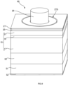
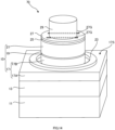
- FIG. 1 is a perspective view of a vertical cavity surface emitting laser (VCSEL, hereinafter also simply referred to as a surface emitting laser) 10 according to Embodiment 1.
- VCSEL vertical cavity surface emitting laser
- a substrate 11 is a gallium-nitride-based semiconductor substrate, for example, a GaN substrate.
- the substrate 11 is, for example, a substrate having a rectangular upper surface shape.
- a first multilayer reflector 13 made of a semiconductor layer that has been grown on the substrate 11 is formed.
- the first multilayer reflector 13 is a semiconductor multilayer reflector in which a low refractive-index semiconductor film having a composition of AlInN and a high refractive-index semiconductor film having a GaN composition and having a refractive index higher than that of the low refractive-index semiconductor film are alternately laminated.
- the first multilayer reflector 13 is a Distributed Bragg Reflector (DBR) made of a semiconductor material.
- DBR Distributed Bragg Reflector
- a buffer layer having the GaN composition is disposed, and alternately forming films of the high refractive-index semiconductor film and the low refractive-index semiconductor film described above on the buffer layer forms the first multilayer reflector 13.
- the upper surface of the substrate 11, that is, the surface on which the buffer layer having the GaN composition is disposed is preferred to be a C-plane or a surface offset by within 0.5° from the C-plane. This is for providing, for example, satisfactory crystallinity of a semiconductor structure layer 15, which will be described later.
- the semiconductor structure layer 15 is a laminated structure made of a plurality of semiconductor layers formed on the first multilayer reflector 13.
- the semiconductor structure layer 15 has an n-type semiconductor layer (a first semiconductor layer) 17 formed on the first multilayer reflector 13, a light-emitting layer (or an active layer) 19 formed on the n-type semiconductor layer 17, and a p-type semiconductor layer (a second semiconductor layer) 21 formed on the active layer 19.
- the n-type semiconductor layer 17 is a semiconductor layer formed on the first multilayer reflector 13.
- the n-type semiconductor layer 17 is a semiconductor layer that has the GaN composition and is doped with Si as n-type impurities.
- the n-type semiconductor layer 17 has a prismatic-shaped lower portion 17A and a column-shaped upper portion 17B disposed on the lower portion 17A.
- the n-type semiconductor layer 17 has the column-shaped upper portion 17B projecting from an upper surface 17S of the prismatic-shaped lower portion 17A.
- the n-type semiconductor layer 17 has a mesa-shaped structure including the upper portion 17B.
- the active layer 19 is a layer that is formed on the upper portion 17B of the n-type semiconductor layer 17 and has a quantum well structure including a well layer having an InGaN composition and a barrier layer having the GaN composition. In a surface emitting laser 10, a light is generated in the active layer 19.
- the p-type semiconductor layer 21 is a semiconductor layer having the GaN composition formed on the active layer 19.
- the p-type semiconductor layer 21 is doped with Mg as p-type impurities.
- An n-electrode 23 is a metal electrode that is disposed on the upper surface 17S of the lower portion 17A of the n-type semiconductor layer 17 and is electrically connected to the n-type semiconductor layer 17.
- the n-electrode 23 is formed into a ring shape so as to surround the upper portion 17B of the n-type semiconductor layer 17.
- An insulating layer 25 is a layer made of an insulator formed on the p-type semiconductor layer 21.
- the insulating layer 25 is formed of, for example, a substance having a refractive index lower than that of a material forming the p-type semiconductor layer 21, such as SiO 2 .
- the insulating layer 25 is formed into a ring shape on the p-type semiconductor layer 21 and is provided with an opening (not illustrated) that exposes the p-type semiconductor layer 21 at the center portion.
- a p-electrode 27 is a metal electrode formed on the insulating layer 25.
- the p-electrode 27 is electrically connected to an upper surface of the p-type semiconductor layer 21 exposed from the above-described opening of the insulating layer 25 via a transparent electrode (not illustrated) made of a metal oxide film, such as ITO or IZO.
- a second multilayer reflector 29 is a dielectric multilayer reflector in which a low refractive index dielectric film made of Al 2 O 3 and a high refractive index dielectric film made of TazOs and having a refractive index higher than that of the low refractive index dielectric film are alternately laminated.
- the second multilayer reflector 29 is the Distributed Bragg Reflector (DBR) made of a dielectric material.
- DBR Distributed Bragg Reflector
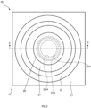
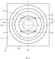
- FIG. 2 is a top view of the surface emitting laser 10.
- the surface emitting laser 10 has the semiconductor structure layer 15 including the n-type semiconductor layer 17 formed on the substrate 11 having the rectangular upper surface shape, the active layer 19 having the circular-shaped upper surface, and the p-type semiconductor layer 21 (see FIG. 1 ).
- the insulating layer 25 and the p-electrode 27 are formed on the p-electrode 27 .
- the second multilayer reflector 29 is formed on the p-electrode 27, the second multilayer reflector 29 is formed.
- the insulating layer 25 has an opening 25H as a circular-shaped opening that exposes the p-type semiconductor layer 21 of the above-described insulating layer 25.
- the opening 25H is formed at the center of the insulating layer 25 when viewed from an upper side of the surface emitting laser 10 and is covered with the second multilayer reflector 29 when viewed from the upper side of the surface emitting laser 10.
- the opening 25H is covered with the second multilayer reflector 29 in the upper surface of the p-type semiconductor layer 21.
- the opening 25H is formed in a region opposed to a lower surface of the multilayer reflector 29 of the insulating layer 25.
- the p-electrode 27 is formed at the center of the insulating layer 25 when viewed from the upper side of the surface emitting laser 10 and has an opening 27H that surrounds the opening 25H. That is, the opening 27H is an opening larger than the opening 25H.
- the opening 27H has a circular shape concentric to the shape of the opening 25H.
- a groove 15G in a circular ring shape is formed on the upper surface of the p-type semiconductor layer 21, that is, the upper surface of the semiconductor structure layer 15.
- the groove 15G is formed in an outside region of the opening 25H and the opening 27H. That is, the groove 15G is a groove provided in a ring shape when viewed from a direction perpendicular to an in-plane direction of the semiconductor structure layer 15.
- the groove 15G is formed so as to be covered by the second multilayer reflector 29 on the upper surface of the p-type semiconductor layer 21. That is, in this embodiment, the groove 15G is formed at a position opposed to a lower surface of the second multilayer reflector 29.
- FIG. 3 is a cross-sectional view of the surface emitting laser 10 taken along the line 3-3 in FIG. 2 .
- the surface emitting laser 10 has the substrate 11 as the GaN substrate, and the first multilayer reflector 13 is formed on the substrate 11. Note that a lower surface of the substrate 11 may be applied with an AR coating.
- the semiconductor structure layer 15 is formed on the first multilayer reflector 13.
- the semiconductor structure layer 15 is a laminated body made by forming the n-type semiconductor layer 17, the active layer 19, and the p-type semiconductor layer 21 in this order.
- the groove 15G formed in the semiconductor structure layer 15 is formed so as to surround a projecting portion 21P projecting at the center on the upper surface of the p-type semiconductor layer 21 and passes through the active layer 19 from the upper surface of the p-type semiconductor layer 21 to reach the n-type semiconductor layer 17.
- the groove 15G is formed so as to pass through the active layer 19.
- the groove 15G forms a clearance in the active layer 19.
- the insulating layer 25 is formed so as to cover the upper surface of the p-type semiconductor layer 21 and an inner surface of the groove 15G. As described above, the insulating layer 25 is made of a material having a refractive index lower than that of the p-type semiconductor layer 21.
- the insulating layer 25 has the opening 25H that exposes the projecting portion 21P. For example, as illustrated in FIG. 2 , the opening 25H is in a circular shape.
- the opening 25H and the projecting portion 21P have similar shapes, and an inner surface of the opening 25H and an outer surface of the projecting portion 21P are in contact with one another.
- a light transmissive electrode layer 31 is a layer made of a conductive body having translucency formed so as to cover the insulating layer 25 and the projecting portion 21P exposed from the opening 25H of the insulating layer 25. That is, the light transmissive electrode layer 31 is electrically in contact with the p-type semiconductor layer 21 in a region exposed by the opening 25H on the upper surface of the p-type semiconductor layer 21.
- the light transmissive electrode layer 31 is formed of, for example, a metal oxide having translucency relative to an emitted light from the active layer 19, such as ITO or IZO.
- the p-electrode 27 is the metal electrode and is formed so as to cover the light transmissive electrode layer 31. That is, the p-electrode 27 is electrically in contact with the light transmissive electrode layer 31. Accordingly, the p-electrode 27 is electrically in contact with or electrically connected to the p-type semiconductor layer 21 via the light transmissive electrode layer 31 in a region exposed by the opening 25H on the upper surface of the p-type semiconductor layer 21.
- the p-electrode 27 has the opening 27H that exposes the light transmissive electrode layer 31 at the center.
- the opening 27H is an opening with a width larger than that of the opening 25H.
- the second multilayer reflector 29 is formed so as to cover the opening 27H and the groove 15G.
- the second multilayer reflector 29 is formed so as to fill a space formed of the opening 27H and so as to be in contact with the light transmissive electrode layer 31.
- the second multilayer reflector 29 is formed so as to fill a space formed of the groove 15G.
- the first multilayer reflector 13 has reflectivity slightly lower than that of the second multilayer reflector 29. Accordingly, a part of the light resonated between the first multilayer reflector 13 and the second multilayer reflector 29 transmits through the first multilayer reflector 13 and the substrate 11 to be taken out to the outside.
- the groove 15G is formed so as to pass through the active layer 19. In other words, the groove 15G forms the clearance in the active layer 19.
- the groove 15G is formed after the semiconductor structure layer 15 is formed. Afterwards, the insulating layer 25 is formed before the light transmissive electrode layer 31, the p-electrode 27, and the second multilayer reflector 29 are formed.
- forming the groove 15G that reaches the active layer 19 forms a space or the clearance in a direction along an in-plane of the active layer 19.
- This clearance reduces a distortion generated in an in-layer direction of the active layer 19 or in a layer surface direction of the semiconductor structure layer 15 when the active layer 19 is formed.
- the active layer 19 has a crystalline structure distorted by a difference of lattice constants between InGaN and GaN forming the quantum well structure when the active layer 19 is formed to cause a piezoelectric polarization to cause a piezoelectric field.
- the generation of this piezoelectric field lowers a recombination probability of the electrons and the holes injected to the light-emitting layer to contribute to lower the internal quantum efficiency.
- the groove 15G reaching the active layer 19 is formed in the semiconductor structure layer 15.
- the clearance by this groove is considered to reduce the distortion generated in the in-layer direction of the active layer 19 during the growth of the active layer 19, and thus, the internal quantum efficiency in the active layer 19 is improved.
- the surface emitting laser 10 when a voltage is applied between the n-electrode 23 and the p-electrode 27, a current flows inside the semiconductor structure layer 15 as indicated by the one-dot chain bold line in the drawing, and the light is emitted from the active layer 19.
- the light emitted from the active layer 19 is repeatedly reflected between the first multilayer reflector 13 and the second multilayer reflector 29 to reach a resonant state (to laser oscillate).
- the current is injected only from a portion exposed by the opening 25H to the p-type semiconductor layer 21. Since the p-type semiconductor layer 21 is considerably thin, the current hardly spreads in the in-plane direction, that is, the direction along the in-plane of the semiconductor structure layer 15 inside the p-type semiconductor layer 21. Accordingly, in the surface emitting laser 10, the current is supplied only to the region immediately below the opening 25H in the active layer 19, and the light is emitted only from this region. That is, in the surface emitting laser 10, the opening 25H has a current confinement structure that restricts a supply range of the current in the active layer 19.
- the first multilayer reflector 13 has the reflectivity slightly lower than that of the second multilayer reflector 29. Accordingly, a part of the light resonated between the first multilayer reflector 13 and the second multilayer reflector 29 transmits through the first multilayer reflector 13 and the substrate 11 to be taken out to the outside.
- the surface emitting laser 10 emits the light from the lower surface of the substrate 11 toward the direction perpendicular to the lower surface of the substrate 11 and the in-plane direction of the respective layers of the semiconductor structure layer 15.
- the projecting portion 21P of the p-type semiconductor layer 21 of the semiconductor structure layer 15 and the opening 25H of the insulating layer 25 define a luminescence center as a center of a light emission region in the active layer 19 to define a center axis (a luminescence center axis) AX of a resonator OC.
- the center axis AX of the resonator OC passes through a center of the projecting portion 21P of the p-type semiconductor layer 21 and extends along a direction perpendicular to the in-plane direction of the semiconductor structure layer 15.
- the light emission region of the active layer 19 means, for example, a region having a predetermined width from which a light having a predetermined intensity or more is emitted in the inside of the active layer 19, and its center is the luminescence center.
- the light emission region of the active layer 19 means is a region to which a current having a predetermined density or more is injected in the inside of the active layer 19, and its center is the luminescence center.
- a straight line that passes through the luminescence center and is perpendicular to the upper surface of the substrate 11 or the in-plane direction of the respective layers of the semiconductor structure layer 15 is the center axis AX.
- the luminescence center axis AX is a straight line extending along a resonator length direction of the resonator OC constituted of the first multilayer reflector 13 and the second multilayer reflector 29.
- the center axis AX corresponds to an optical axis of the laser light emitted from the surface emitting laser 10.
- the first multilayer reflector 13 is made of a GaN base layer of 1 ⁇ m and 42 pairs of n-GaN layers and AlInN layers formed on the upper surface of the substrate 11.
- the n-type semiconductor layer 17 is an n-GaN layer having a layer thickness of 1580 nm.
- the active layer 19 is made of an active layer having a multiple quantum well structure in which four pairs of GaInN layers of 4 nm and GaN layers of 5 nm are laminated.
- an AlGaN electronic barrier layer doped with Mg is formed, and the p-type semiconductor layer 21 made of a p-GaN layer of 50 nm is formed thereon.
- the second multilayer reflector 29 is a lamination of 10.5 pairs of Nb 2 O 5 and SiO 2 .
- the resonant wavelength in this case was 440 nm.
- the groove portion 15G formed in the semiconductor structure layer 15 has an outer diameter of 8 ⁇ m, a depth of 120 nm, and a width of 2 ⁇ m.
- the light transmissive electrode layer 31 formed on the semiconductor structure layer 15 is a layer made of ITO of 20 nm, and the second multilayer reflector 29 is formed on the light transmissive electrode layer 31 and the p-electrode 27 with a spacer layer of Nb 2 O 5 of 40 nm interposed.
- Aback surface of the substrate 11 is a polished surface, and two layers of AR coatings of Nb 2 O 5 and SiO 2 are formed on this polished surface.
- the p-type semiconductor layer 21 may have a layer thickness of 50 nm in the projecting portion 21P and a layer thickness of 30 nm in the other portions. That is, the p-type semiconductor layer 21 may have different layer thicknesses in the projecting portion 21P and the other regions.
- the insulating layer 25 has an upper surface configured to be arranged at a height position identical to an upper surface of the projecting portion 21P of the p-type semiconductor layer 21. These are merely one example.
- the insulating layer 25 has a refractive index lower than that of the p-type semiconductor layer 21.
- Layer thicknesses of the other layers between the first multilayer reflector 13 and the second multilayer reflector 29 are the same at any positions in the plane insofar as in the same layer.
- an equivalent refractive index (an optical distance between the first multilayer reflector 13 and the second multilayer reflector 29, and corresponds to a resonant wavelength) in the resonator OC formed between the first multilayer reflector 13 and the second multilayer reflector 29 of the surface emitting laser 10 differs in a column-shaped central region CA having an upper surface shape defined by the opening 25H and in a pipe-shaped peripheral region PA around the central region CA by a difference in refractive indexes between the p-type semiconductor layer 21 and the insulating layer 25.
- the equivalent refractive index in the peripheral region PA is lower than the equivalent refractive index in the central region, that is, an equivalent resonant wavelength in the central region CA is smaller than the equivalent resonant wavelength in the peripheral region PA.
- the light emission region where the light is emitted in the active layer 19 is a portion overlapping with the central region CA in the active layer 19, in other words, a region inside the opening 25H of the insulating layer 25 in top view.
- the central region CA including the light emission region of the active layer 19 and the peripheral region PA that surrounds the central region CA and has the refractive index lower than that of the central region CA are formed.
- the groove 15G that reaches the active layer 19 from the upper surface of the p-type semiconductor layer 21 is formed in the semiconductor structure layer 15.
- this groove 15G the distortion generated in the in-layer direction of the active layer 19 is reduced in the active layer 19, and the internal quantum efficiency in the active layer 19 is improved, thereby ensuring achieving improved luminous efficiency.
- n-GaN substrate is prepared as the substrate 11, and an n-GaN layer (a layer thickness of 1 ⁇ m) is formed as a base layer on the substrate by Metal-Organic Vapor Phase Epitaxy method (MOVPE). Subsequently, 42 pairs of n-GaN/AlInN layers are film-formed on the base layer to form the first multilayer reflector 13.
- MOVPE Metal-Organic Vapor Phase Epitaxy method
- the active layer 19 is formed by forming Si-doped n-GaN (a layer thickness of 1580 nm) on the first multilayer reflector 13 to form the n-type semiconductor layer 17 and then, laminating four pairs of layers made of GaInN (a layer thickness of 4 nm) and GaN (a layer thickness of 5 nm) on the n-type semiconductor layer 17.
- the electronic barrier layer (not illustrated) made of Mg-doped AlGaN is formed on the active layer 19, and then, p-GaN layer (a layer thickness of 50 nm) is film-formed on the electronic barrier layer to form the p-type semiconductor layer 21.
- a peripheral portion of the p-type semiconductor layer 21, the active layer 19, and the n-type semiconductor layer 17 is etched to form a mesa shape such that the upper surface 17S of the n-type semiconductor layer 17 is exposed in the peripheral portion.
- the semiconductor structure layer 15 including the column-shaped portion made of the n-type semiconductor layer 17, the active layer 19, and the p-type semiconductor layer 21 in FIG. 1 is completed.
- the groove 15G passing through the active layer 19 from the upper surface of the p-type semiconductor layer 21 is formed by etching.
- the insulating layer 25 is formed by forming a film of SiO 2 on the semiconductor structure layer 15 and removing a part of the film to form the opening 25H.
- the light transmissive electrode layer 31 is formed by forming film of ITO of 20 nm on the insulating layer 25, and then, the p-electrode 27 and the n-electrode 23 are formed by forming films of Au on the light transmissive electrode layer 31 and on the upper surface 17S of the n-type semiconductor layer 17, respectively.
- Nb 2 O 5 of 40 nm is film-formed as a spacer layer (not illustrated) on the p-electrode 27 and the light transmissive electrode layer 31, and then, by forming a film of 10.5 pairs of layers made of Nb 2 O 5 /SiO 2 in one pair on the spacer layer, the second multilayer reflector 29 is formed.
- the back surface of the substrate 11 is polished, and then, by forming an AR coating made of Nb 2 O 5 /SiO 2 on the polished surface, the surface emitting laser 10 is completed.
- the surface emitting laser 40 is different from the surface emitting laser 10 in that the groove 15G of the semiconductor structure layer 15 is formed outside the second multilayer reflector 29 in top view.
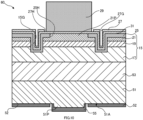
- FIG. 4 illustrates a perspective view of the surface emitting laser 40 according to Embodiment 2.
- FIG. 5 illustrates a cross-sectional view of the surface emitting laser 40 cut along a cross section similar to the one illustrated in Embodiment 1 described above.
- the groove 15G of the semiconductor structure layer 15 is formed outside the second multilayer reflector 29 on the upper surface of the p-type semiconductor layer 21. That is, on the upper surface of the p-type semiconductor layer 21, the groove 15G is exposed from a second formation region.
- a groove structure 27G formed by inheriting the shape of the groove 15G is formed on an upper surface of the p-electrode 27 formed on the p-type semiconductor layer 21 via the insulating layer 25, a groove structure 27G formed by inheriting the shape of the groove 15G is formed. That is, the groove structure 27G is formed on the groove 15G in a shape approximately identical to that of the groove 15G.
- the groove 15G that reaches the active layer 19 from the upper surface of the p-type semiconductor layer 21 is formed in the semiconductor structure layer 15.
- the distortion generated in the in-layer direction of the active layer 19 is reduced in the active layer 19, and the internal quantum efficiency in the active layer 19 is improved, thereby ensuring achieving improved luminous efficiency.
- the following describes a surface emitting laser 50 as Embodiment 3 of the present invention.
- the surface emitting laser 50 is different from the surface emitting laser 10 in that the electrode connected to the n-type semiconductor layer 17 is disposed on the back surface of the substrate 51 or the like.
- FIG. 6 is a perspective view of the surface emitting laser 50.
- a substrate 51 is, for example, a substrate having a rectangular upper surface shape.
- the substrate 51 is a substrate made of a conductive material such as n-GaN.
- an n-electrode 52 made of metal is formed on a back surface of the substrate 51.
- the first multilayer reflector 53 is a semiconductor multilayer reflector with conductivity in which a low refractive-index semiconductor film having a composition of AlInN and a high refractive-index semiconductor film having an n-GaN composition and having a refractive index higher than that of the low refractive-index semiconductor film are alternately laminated.
- the first multilayer reflector 53 is the Distributed Bragg Reflector (DBR) made of a semiconductor material.
- DBR Distributed Bragg Reflector
- a buffer layer having an n-GaN composition is disposed, and alternately forming films of the high refractive-index semiconductor film and the low refractive-index semiconductor film described above on the buffer layer forms the first multilayer reflector 53.
- the semiconductor structure layer 15 is a laminated structure made of a plurality of semiconductor layers formed on the first multilayer reflector 53.
- the semiconductor structure layer 15 has the n-type semiconductor layer (the first semiconductor layer) 17 formed on the first multilayer reflector 53, the light-emitting layer (or the active layer) 19 formed on the n-type semiconductor layer 17, and the p-type semiconductor layer (the second semiconductor layer) 21 formed on the active layer 19.
- the n-type semiconductor layer 17 is a semiconductor layer formed on the first multilayer reflector 53.
- the n-type semiconductor layer 17 is a semiconductor layer that has the GaN composition and is doped with Si as n-type impurities.
- the active layer 19 is a layer that is formed on the n-type semiconductor layer 17 and has the quantum well structure including the well layer having the InGaN composition and the barrier layer having the GaN composition. In the surface emitting laser 50, a light is generated in the active layer 19.
- the p-type semiconductor layer 21 is a semiconductor layer having the GaN composition formed on the active layer 19.
- the p-type semiconductor layer 21 is doped with Mg as p-type impurities.
- the insulating layer 25 is a layer made of the insulator formed on the p-type semiconductor layer 21.
- the insulating layer 25 is formed of, for example, a substance having a refractive index lower than that of the material forming the p-type semiconductor layer 21, such as SiO 2 .
- the insulating layer 25 is formed into a ring shape on the p-type semiconductor layer 21 and is provided with the opening (not illustrated) that exposes the p-type semiconductor layer 21 at the center portion.
- the p-electrode 27 is a metal electrode formed on the insulating layer 25.
- the p-electrode 27 is electrically connected to the upper surface of the p-type semiconductor layer 21 exposed from the above-described opening of the insulating layer 25 via the transparent electrode (not illustrated) made of the metal oxide film, such as ITO or IZO.
- the second multilayer reflector 29 is a dielectric multilayer reflector in which the low refractive index dielectric film made of Al 2 O 3 and the high refractive index dielectric film made of TazOs and having a refractive index higher than that of the low refractive index dielectric film are alternately laminated.
- the second multilayer reflector 29 is the Distributed Bragg Reflector (DBR) made of a dielectric material.
- DBR Distributed Bragg Reflector
- FIG. 7 is a top view of the surface emitting laser 50.
- the surface emitting laser 50 has the semiconductor structure layer 15 including the n-type semiconductor layer 17 formed above the substrate 51 having the rectangular upper surface shape, the active layer 19, and the p-type semiconductor layer 21 (see FIG. 6 ).
- the insulating layer 25 and the p-electrode 27 are formed on the p-electrode 27 .
- the second multilayer reflector 29 is formed on the p-electrode 27, the second multilayer reflector 29 is formed.
- the insulating layer 25 has the opening 25H as a circular-shaped opening that exposes the p-type semiconductor layer 21 of the above-described insulating layer 25.
- the opening 25H is formed at the center of the insulating layer 25 when viewed from an upper surface of the surface emitting laser 10 and is covered with the second multilayer reflector 29 when viewed from the upper surface of the surface emitting laser 10.
- the opening 25H is covered with the second multilayer reflector 29 on the upper surface of the p-type semiconductor layer 21.
- the opening 25H is disposed in a region opposed to the lower surface of the multilayer reflector 29 of the upper surface of the p-type semiconductor layer 21.
- the p-electrode 27 is formed at the center of the insulating layer 25 when viewed from the upper surface of the surface emitting laser 50 and has the opening 27H that surrounds the opening 25H. That is, the opening 27H is an opening larger than the opening 25H.
- the opening 27H has a circular shape concentric to the shape of the opening 25H.
- a groove 15G in a circular ring shape is formed on the upper surface of the p-type semiconductor layer 21, that is, on the upper surface of the semiconductor structure layer 15.
- the groove 15G is formed in an outside region of the opening 25H and the opening 27H.
- the groove 15G is formed so as to be covered with the second multilayer reflector 29 on the upper surface of the p-type semiconductor layer 21. That is, in this embodiment, the groove 15G is formed at a position opposed to the lower surface of the second multilayer reflector 29.
- FIG. 8 is a cross-sectional view of the surface emitting laser 50 taken along the line 8-8 in FIG. 7 .
- the surface emitting laser 50 has the substrate 51 as the n-GaN substrate, and the first multilayer reflector 53 is formed on the substrate 51.
- a projecting portion 51P is formed in a region corresponding to the projecting portion 21P when viewed from a normal direction of the substrate 51.
- the projecting portion 51P is a protrusion remained due to a removal of a peripheral area of the projecting portion 51P by dry etching after the back surface 51A is polished. Accordingly, a top surface of the projecting portion 51P is a polished surface, and the peripheral region of the projecting portion 51P of the back surface 51A of the substrate 51 has a surface where the polished surface is dry-etched.
- the n-electrode 52 is formed in the peripheral region of the projecting portion 51P of the back surface 51A of the substrate 51, that is, in a region excluding the projecting portion 51P. Because the projecting portion 51P has a top surface serving as an opening through which the emitted light is emitted outside so as not to obstruct the emitted light by the n-electrode 52. That is, the projecting portion 51P has a structure in which it projects from the opening of the n-electrode 52.
- An anti-reflection layer 55 is formed so as to cover the projecting portion 51P in the back surface 51A of the substrate 51.
- the anti-reflection layer 55 is made of, for example, a dielectric multilayer film, and has a structure, for example, in which Ta 2 O 5 layers and SiO 2 layers are alternately laminated a plurality of times.
- the anti-reflection layer 55 is a so-called AR coating that suppresses the light emitted from the active layer 19 from being reflected on the top surface of the projecting portion 51P of the substrate 51.
- the semiconductor structure layer 15 is a laminated structure made by forming the n-type semiconductor layer 17, the active layer 19, and the p-type semiconductor layer 21 in this order.
- the p-type semiconductor layer 21 has the projecting portion 21P projecting upward in a columnar shape at the center of the upper surface of the p-type semiconductor layer 21.
- the groove 15G formed in the semiconductor structure layer 15 is formed so as to surround the projecting portion 21P on the upper surface of the p-type semiconductor layer 21 and passes through the active layer 19 from the upper surface of the p-type semiconductor layer 21 to reach the n-type semiconductor layer 17.
- the groove 15G is formed so as to pass through the active layer 19. In other words, the groove 15G forms the clearance in the active layer 19.
- the insulating layer 25 is formed so as to cover the upper surface of the p-type semiconductor layer 21 and the inner surface of the groove 15G. As described above, the insulating layer 25 is made of a material having a refractive index lower than that of the p-type semiconductor layer 21.
- the insulating layer 25 has the opening 25H that exposes the projecting portion 21P. For example, as illustrated in FIG. 7 , the opening 25H is in a circular shape.
- the opening 25H and the projecting portion 21P have similar shapes, and the inner surface of the opening 25H and the outer surface of the projecting portion 21P are in contact with one another.
- the light transmissive electrode layer 31 is a layer made of a conductive body having translucency formed to cover the insulating layer 25 and the projecting portion 21P exposed from the opening 25H of the insulating layer 25.
- the light transmissive electrode layer 31 is formed of, for example, a metal oxide having translucency relative to the emitted light from the active layer 19, such as ITO or IZO.
- the p-electrode 27 is the metal electrode and is formed so as to cover the light transmissive electrode layer 31.
- the p-electrode 27 has the opening 27H that exposes the light transmissive electrode layer 31 at the center.
- the opening 27H is an opening with a width larger than that of the opening 25H.
- the second multilayer reflector 29 is formed so as to cover the opening 27H and the groove 15G.
- the second multilayer reflector 29 is formed so as to fill a space formed of the opening 27H and so as to be in contact with the light transmissive electrode layer 31.
- the second multilayer reflector 29 is formed so as to fill a space formed of the groove 15G.
- the first multilayer reflector 53 has reflectivity slightly lower than that of the second multilayer reflector 29. Accordingly, a part of the light resonated between the first multilayer reflector 53 and the second multilayer reflector 29 transmits through the first multilayer reflector 53 and the substrate 51 to be taken out to the outside.
- the groove 15G is formed so as to pass through the active layer 19. In other words, the groove 15G forms the clearance in the active layer 19.
- the groove 15G is formed after the semiconductor structure layer 15 is formed. Afterwards, the insulating layer 25 is formed before the light transmissive electrode layer 31, the p-electrode 27, and the second multilayer reflector 29 are formed.
- forming the groove 15G that reaches the active layer 19 forms the clearance in a direction along the in-plane direction of the active layer 19.
- This clearance reduces a distortion generated in the in-layer direction of the active layer 19 or in the in-plane direction of the semiconductor structure layer 15 when the active layer 19 is formed.
- the active layer 19 has a crystalline structure distorted by the difference of lattice constants between InGaN and GaN forming the quantum well structure when the active layer 19 is formed, which causes the piezoelectric polarization so as to generate the piezoelectric field.
- This piezoelectric field lowers the recombination probability of the electrons and the hole injected to the light-emitting layer to lower the internal quantum efficiency.
- the groove 15G reaching the active layer 19 is formed in the semiconductor structure layer 15.
- the clearance by this groove is considered to reduce the distortion generated in the in-layer direction of the active layer 19 during the growth of the active layer 19, and thus, the internal quantum efficiency in the active layer 19 is improved.
- the surface emitting laser 50 when a voltage is applied between the n-electrode 52 and the p-electrode 27, a current flows inside the semiconductor structure layer 15 as indicated by the one-dot chain bold line in the drawing, and the light is emitted from the active layer 19.
- the light emitted from the active layer 19 is repeatedly reflected between the first multilayer reflector 53 and the second multilayer reflector 29 to reach a resonant state (to laser oscillate).
- the first multilayer reflector 53 has the reflectivity slightly lower than that of the second multilayer reflector 29. Accordingly, a part of the light resonated between the first multilayer reflector 53 and the second multilayer reflector 29 transmits through the first multilayer reflector 53 and the substrate 51 to be taken out to the outside from the projecting portion 51P.
- the surface emitting laser 50 emits the light toward the direction perpendicular to the lower surface of the substrate 51 and the in-plane direction of the respective layers of the semiconductor structure layer 15.
- the first multilayer reflector 53 is made of the n-GaN base layer of 1 ⁇ m and 42 pairs of n-GaN layers and AlInN layers formed on the surface of the substrate 51.
- the n-type semiconductor layer 17 is the n-GaN layer doped with Si having a layer thickness of 1580 nm.
- the active layer 19 is made of an active layer having a multiple quantum well structure in which four pairs of GaInN layers of 4 nm and GaN layers of 5 nm are laminated.
- the AlGaN electronic barrier layer doped with Mg is formed, and the p-type semiconductor layer 21 made of the p-GaN layer of 50 nm is formed thereon.
- the second multilayer reflector 29 is a lamination of 10.5 pairs of and SiO 2 .
- the groove portion 15G formed in the semiconductor structure layer 15 has an outer diameter of 20 ⁇ m, a depth of 120 nm, and a width of 1 ⁇ m.
- the light transmissive electrode layer 31 formed on the semiconductor structure layer 15 is a layer made of ITO of 20 nm, and the second multilayer reflector 29 is formed on the light transmissive electrode layer 31 and the p-electrode 27 with the spacer layer of NbzOs of 40 nm interposed.
- the p-type semiconductor layer 21 may have a layer thickness of 50 nm in the projecting portion 21P and a layer thickness of 30 nm in the other regions. That is, the p-type semiconductor layer 21 may have different layer thicknesses in the projecting portion 21P and the other regions.
- the insulating layer 25 has an upper surface configured to be arranged at a height position identical to the upper surface of the projecting portion 21P of the p-type semiconductor layer 21. These are merely one example.
- the groove 15G that reaches the active layer 19 from the upper surface of the p-type semiconductor layer 21 is formed in the semiconductor structure layer 15.
- this groove 15G the distortion generated in the in-layer direction of the active layer 19 is reduced in the active layer 19, and the internal quantum efficiency in the active layer 19 is improved, thereby ensuring achieving improved luminous efficiency.
- the following describes a surface emitting laser 60 according to Embodiment 4.
- the surface emitting laser 60 is different from the surface emitting laser 50 in that the groove 15G of the semiconductor structure layer 15 is formed on an outside of the second multilayer reflector 29 in top view.
- FIG. 9 illustrates a perspective view of the surface emitting laser 60 according to Embodiment 4.
- FIG. 10 illustrates a cross-sectional view of the surface emitting laser 60 cut along a cross section similar to the one illustrated in Embodiment 3 described above.
- the groove 15G of the semiconductor structure layer 15 is formed outside the second multilayer reflector 29 on the upper surface of the p-type semiconductor layer 21. That is, on the upper surface of the p-type semiconductor layer 21, the groove 15G is exposed on the outside of the second multilayer reflector.
- the groove structure 27G formed by inheriting the shape of the groove 15G is formed on the groove 15G in a shape approximately identical to that of the groove 15G.
- the groove 15G that reaches the n-type semiconductor layer 17 from the upper surface of the p-type semiconductor layer 21 is formed in the semiconductor structure layer 15.
- the groove 15G formed in the semiconductor structure layer 15 has a circular ring shape.
- the groove 15G may have other shapes.
- the groove 15G may be a groove structure including a recessed portion GV (or a groove GV) formed intermittently instead of a perfect ring in a ring-shaped region CR (the region enclosed by the one-dot chain line in the drawing). That is, the groove 15G may have a recessed structure including a plurality of recessed portions. In other words, the groove 15G may have a ring-shaped structure formed intermittently. For example, the groove 15G may have an intermittently formed ring-shaped structure that surrounds a region exposed by the opening 25H of the upper surface of the p-type semiconductor layer 21.
- the plurality of recessed portions are preferably formed in two or more directions when viewed from the above-described luminescence center axis AX. That is, when the groove 15G is formed by the plurality of recessed portions, in top view of the surface emitting laser 10, the recessed portions are preferably formed in two or more directions when viewed from the light emission region including the luminescence center axis AX and have a structure that sandwiches the light emission region between the recessed portions.
- the recessed portions forming the groove 15G are further preferably disposed rotationally symmetrically with respect to the luminescence center axis AX. In other words, the recessed portions forming the groove 15G are preferably disposed rotationally symmetrically when viewed from a direction perpendicular to the in-plane direction of the semiconductor structure layer 15.
- the distortion in the active layer 19 is also possible to make a degree of reduction of the distortion in the active layer 19 anisotropic to control polarization of the light emitted from the surface emitting laser of the above-described embodiments by changing the shape of the groove 15G, for example, by forming the groove 15G with the plurality of recessed portions.
- the distortion of the active layer 19 is further reduced in a direction where the recessed portion GV forming the groove 15G exists. This allows increasing an optical gain in a direction (the right-left direction in the drawing) where the recessed portion GV forming the groove 15G exists when viewed from the opening 25H and obtaining a large amount of light having a polarization direction along the direction.
- the groove 15G is preferably formed near the luminescence center axis AX. Accordingly, for example, like the surface emitting laser 10 according to Embodiment 1 and the surface emitting laser 50 according to Embodiment 3, the groove 15G is preferably formed below the second multilayer reflector 29.
- the groove 15G or the plurality of grooves GV are preferably formed, for example, at a distance within 50 ⁇ m from an outer edge of the light emission region. That is, the ring-shaped region CR forming the groove 15G is preferably disposed at a distance within 50 ⁇ m from the outer edge of the light emission region or the central region CA.
- a configuration in which a ring-shaped laser light is emitted may be employed. That is, when viewed from above the surface emitting laser of the above-described embodiment, a circular-shaped insulating layer may be formed at the center of the opening 25H of the insulating layer 25. Yet in other words, the insulating layer 25 may have a circular ring-shaped hole portion, and via the circular ring-shaped hole portion, the upper surface of the p-type semiconductor layer 21 may be exposed, and the light transmissive electrode layer 31 and the p-type semiconductor layer 21 may be electrically in contact with one another.
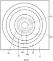
- an inside recessed portion IG may be further formed inside the groove 15G of the semiconductor structure layer 15. This recessed portion IG also passes through the active layer 19 from the upper surface of the p-type semiconductor layer 21 similarly to the groove 15G.
- FIG. 12 is a top view of a modification in which a column-shaped inside recessed portion IG is formed in the surface emitting laser 10 according to Embodiment 1.
- FIG. 13 is a top view of a modification in which a cylindrical-shaped inside recessed portion IG is formed in the surface emitting laser 10 according to Embodiment 1.
- the surface emitting laser 70 of this embodiment is different from the surface emitting laser 10 according to Embodiment 1 in that a C-plane GaN substrate that is inclined (offset) in a m-plane (1-100) direction from c-plane is used as the substrate 11 and an aspect of the groove 15G is different.
- the surface emitting laser 70 can be formed by a manufacturing method similar to that of the surface emitting laser 10 according to Embodiment 1.
- FIG. 14 is a perspective view when viewed from obliquely above in front of the surface emitting laser 70.
- FIG. 15 is a top view of the surface emitting laser 70.
- the surface emitting laser 70 has the substrate 11 whose upper surface is a surface that is offset to the m-plane from the c-plane of a GaN crystal plane.
- the upper surface of the substrate 11 is a surface that is inclined by 0.4° toward the m-plane direction from the c-plane.
- the substrate 11 is a GaN substrate having a principal surface that is offset by 0.4° toward the m-plane from the c-plane.
- an axis AX1 is an axis along an m-axis direction perpendicular to the m-plane of the substrate 11 and in the in-plane including the upper surface of the substrate 11
- an axis AX2 is an axis that is perpendicular to the axis AX1 and in the in-plane including the upper surface of the substrate 11.
- the grooves 15G are constituted of two grooves GV extending parallel to one another along the axis AX2.
- the grooves 15G are constituted of two grooves GV extending with the axis AX2 interposed. That is, in the direction along the axis AX1, the grooves 15G are disposed so as to sandwich the opening 25H of the insulating layer 25 that overlaps with the light emission region of the active layer 19.
- each of the grooves GV extends from a region immediately below the second multilayer reflector 29 up to an outside of the second multilayer reflector 29.
- both end portions of the respective grooves GV are disposed outside the second multilayer reflector 29.
- the groove structures 27G having shapes similar to the grooves 15G also extend from the region immediately below the second multilayer reflector 29 up to the outside of the second multilayer reflector 29.
- no groove GV is formed in a region in the direction along the axis AX2 when viewed from the opening 25H. That is, in the surface emitting laser 70, the grooves GV are formed only in the region in the direction along the axis AX1 when viewed from the opening 25H.
- the following describes the polarization direction of the emitted light in the surface emitting laser 70.
- an optical gain having the polarization direction in the m-axis direction becomes larger than the other direction, and thus, the laser light having the polarization direction in the m-axis direction easily oscillates.
- a large amount of light has the polarization direction in the m-axis direction.
- the surface emitting laser 70 has the groove structures 27G in which the grooves GV are formed only in the region in the direction along the axis AX1 along the m-axis direction when viewed from the opening 25H.
- the distortion of the active layer 19 is significantly reduced.
- the surface emitting laser 70 increases the gain around the direction along the axis AX1 along the m-axis direction and thus, and thus, in addition to an effect by the above-described offset, allows obtaining a large amount of laser light having the polarization direction in the direction along the m-axis direction.
- the upper surface of the substrate 11 is preferably inclined in a range of 0.1° to 0.5° from the c-plane toward the m-plane.
- the surface emitting laser 70 is formed by growing the semiconductor structure layer 15 by a method similar to that of the surface emitting laser 10 according to Embodiment 1 described above, by performing heat treatment after forming the groove 15G, it is possible to obtain a surface emitting laser capable of obtaining a larger amount of laser light having the polarization direction in the direction along the m-axis direction.
- performing heat treatment at temperature of, for example, 500°C allows forming a surface emitting laser capable of obtaining a larger amount of laser light having the polarization direction in the direction along the m-axis direction. It is considered that this is because, in the p-type semiconductor layer 21, among current paths to the active layer 19, the heat treatment increases the conductivity in the current path in the direction along the axis AX1.
- the increase of the conductivity in the current path in the direction along the axis AX1 is due to detachment of hydrogen from p-GaN forming the p-type semiconductor layer 21 exposed in the groove 15G and thus, the increase of the conductivity of the p-type semiconductor layer 21 around the portion exposed from the groove 15G.
- performing the above-described heat treatment allows further increase of the laser light with the polarization direction along the axis AX direction in the surface emitting laser 70.
- the groove 15G is preferably formed in the circular-shaped region of 50 ⁇ m or less from the outer edge/ of the light emission region.
- the groove 15G is preferably formed in a region in which the active layer has emission intensity of 1.8% or less of an emission peak of the active layer when the surface emitting laser is viewed from above.
- the region to form the groove 15G for example, the ring-shaped region CR in FIG. 16 is a region at a distance of 50 ⁇ m or less from the outer edge of the light emission region and is a region in which the active layer has the emission intensity of 1.8% or less of the emission peak of the active layer when the surface emitting laser is viewed from above.
- the groove 15G is preferably formed so as not to overlap with the opening 25H in the direction along the axis AX2.
- generation of reduction of the distortion in the active layer 19 in the direction along the axis AX2 is suppressed and generation of the light having the polarization direction in the direction along the axis AX2 is reduced.
- increasing a difference of reduction of the distortion in the active layer 19 between the direction along the axis AX1 and the direction along the axis AX2 to increase anisotropy of the reduction of the distortion allows increasing a proportion of the light having the polarization direction in the direction along the axis AX1 in the light emitted from the surface emitting laser 70.
- the upper surface of the substrate 11 may be offset from the c-plane to an a-plane as the other non-polar plane.
- the axis AX1 becomes an axis along an a-axis and the groove GV is formed in a region in the direction along the axis AX1 when viewed from the opening 25H.
- the surface emitting laser such as the surface emitting laser 70 according to Embodiment 5 is useful when obtaining a sensor light that requires a light in which the polarization direction is aligned, for example, a light for communication such as Li-Fi.
- the insulating layer 25 is disposed to generate the current confinement by forming the insulating region and to form the region in which the refractive index is low
- the current confinement may be generated and a region in which the refractive index is low may be generated by another method. For example, by etching the surface of the semiconductor structure layer 15 where the insulating layer 25 is disposed in the above-described embodiment, an insulating region and a region in which the refractive index is low may be formed.
- an insulating region and a region having a low refractive index may be formed to generate an effect similar to that of forming the insulating layer 25 in the above-described embodiment.
- ion implantation for example, B ions, Al ions, or oxygen ions are implanted into the semiconductor structure layer 15.
- the semiconductor structure layer 15 may be formed by laminating the p-GaN layer, an active layer similar to that of the above-described embodiment, and the n-GaN layer on the n-type semiconductor layer 17 in this order.
- a tunnel joining layer constituted of an n + -GaN layer and a p + -GaN may be formed in a portion where the central region CA of the above-described embodiment overlaps in top view in a region in contact with the n-type semiconductor layer 17.
Landscapes
- Physics & Mathematics (AREA)
- Condensed Matter Physics & Semiconductors (AREA)
- General Physics & Mathematics (AREA)
- Electromagnetism (AREA)
- Optics & Photonics (AREA)
- Semiconductor Lasers (AREA)
- Led Devices (AREA)
Claims (10)
- Oberflächenlichtemissionselement bzw. Lichtemissionselement mit vertikaler Kavität, welches Folgendes aufweist:ein Galliumnitrid-basiertes Halbleitersubstrat (11);einen ersten mehrlagigen Reflektor bzw. Multilayer-Reflektor (13), der aus einem Nitrid-Halbleiter gemacht ist, der auf dem Substrat (11) geformt ist;eine Halbleiterstrukturschicht (15), die eine erste Halbleiterschicht (17), eine aktive Schicht (19) und eine zweite Halbleiterschicht (21) aufweist, wobei die erste Halbleiterschicht (17) aus einem Nitrid-Halbleiter mit einem ersten Leitfähigkeitstyp gemacht ist, die auf dem ersten Multilayer-Reflektor (13) geformt ist, wobei die aktive Schicht (19) aus einem Nitrid-Halbleiter gemacht ist, der auf der ersten Halbleiterschicht (17) geformt ist, wobei die zweite Halbleiterschicht (21) auf der aktiven Schicht (19) geformt ist und aus einem Nitrid-Halbleiter gemacht ist, der einen zweiten Leitfähigkeitstyp hat, der entgegengesetzt zum ersten Leitfähigkeitstyp ist;eine erste Elektrodenschicht (23), die elektrisch in Kontakt mit der ersten Halbleiterschicht (17) der Halbleiterstrukturschicht (15) ist,eine zweite Elektrodenschicht (31), die auf einer Oberseite der Halbleiterstrukturschicht (15) geformt ist, wobei die zweite Elektrodenschicht (31) mit der zweiten Halbleiterschicht (21) der Halbleiterstrukturschicht (15) in einer Region der Oberseite elektrisch in Kontakt ist; undeinen zweiten Mehrschicht- bzw. Multilayer-Reflektor (29), der so geformt ist, dass er die eine Region auf der zweiten Elektrodenschicht (31) bedeckt, wobei der zweite Multilayer-Reflektor (29) einen Resonator mit dem ersten Multilayer-Reflektor (13) bildet, wobeidie Halbleiterstrukturschicht (15) eine vertiefte Struktur hat, die einen oder eine Vielzahl von vertieften Teilen (15G) hat, der bzw. die durch die aktive Schicht von der Oberseite in einer Region verläuft, welche die eine Region umgibt, undwobei die vertiefte Struktur so angeordnet ist, dass sie mit dem zweiten Multilayer-Reflektor (29) in einer Ansicht von einer Richtung senkrecht zu einer Ebenenrichtung der Halbleiterstrukturschicht (15) überlappt.
- Oberflächenlichtemissionselement nach Anspruch 1, wobei
der eine oder die Vielzahl von vertieften Teilen (15G) in einer Ansicht senkrecht zu einer Ebenenrichtung der Halbleiterstrukturschicht (15) rotationssymmetrisch angeordnet ist bzw. sind. - Oberflächenlichtemissionselement nach Anspruch 1 oder 2, wobei
der eine oder die Vielzahl von vertieften Teilen (15G) Nuten sind, die in einer Ansicht von einer Richtung senkrecht zu einer Ebenenrichtung der Halbleiterstrukturschicht (15) in einer Ringform angeordnet sind. - Oberflächenlichtemissionselement nach einem der Ansprüche 1 bis 3, wobei
eine Region außerhalb der einen Region der Oberseite der Halbleiterstrukturschicht (15) und eine Innenfläche des einen oder der Vielzahl von vertieften Teilen (15G) mit einer Isolierschicht (25) bedeckt sind. - Oberflächenlichtemissionselement nach einem der Ansprüche 1 bis 4, wobei
die eine Region der Oberseite der Halbleiterstrukturschicht (15) eine ringförmige Region ist und eine andere vertiefte Struktur hat, die einen oder eine Vielzahl von vertieften Teilen (15G) aufweist, die durch die aktive Schicht (19) von der Oberseite in der einen Region verläuft bzw. verlaufen. - Oberflächenlichtemissionselement nach einem der Ansprüche 1 bis 5, wobeidie erste Halbleiterschicht eine tafel- bzw. plateauförmige Struktur aufweist, und wobei die plateauförmige Struktur eine aktive Schicht (19) und die zweite Halbleiterschicht (21) aufweist, undwobei die erste Elektrodenschicht (23) auf einer Oberseite der ersten Halbleiterschicht (17) angeordnet ist, die um die plateauförmige Struktur herum vorhanden ist.
- Oberflächenlichtemissionselement nach einem der Ansprüche 1 bis 6, wobeidas Galliumnitrid-basierte Halbleitersubstrat (51) einen ersten Leitfähigkeitstyp hat, undwobei die erste Elektrodenschicht (52) auf einer Oberfläche an einer entgegengesetzten Seite der Halbleiterstrukturschicht (15) des Substrats und an einer Position angeordnet ist, welche eine Region ausschließt, die in einer Ansicht von einer senkrechten Richtung des Substrates der einen Region entspricht.
- Oberflächenlichtemissionselement nach Anspruch 7, wobeidie erste Elektrodenschicht (52) in einer Ansicht von der senkrechten Richtung des Substrates (51) eine Form hat, welche eine Öffnung in eine Region entsprechend der einen Region aufweist, undwobei das Galliumnitrid-basierte Halbleitersubstrat (51) einen vorstehenden Teil (51P) hat, in welchem ein Teil des Substrates aus der Öffnung hervorsteht.
- Oberflächenlichtemissionselement nach Anspruch 1, wobei
der erste Halbleiterreflektor (13) auf einer c-Ebene des Galliumnitridbasierten Halbleitersubstrates (11) oder auf einer Oberfläche geformt ist, die innerhalb von 0,5° von der c-Ebene versetzt ist. - Oberflächenlichtemissionselement nach Anspruch 1, wobei
die vertiefte Struktur eine ringförmige Struktur ist, die aus einer Vielzahl von intermittierend geformten Nutenteilen (GV) gebildet wird, welche die eine Region umgeben.
Priority Applications (1)
| Application Number | Priority Date | Filing Date | Title |
|---|---|---|---|
| EP24196996.3A EP4451488B1 (de) | 2020-01-08 | 2020-12-18 | Lichtemittierendes element mit vertikalem resonator |
Applications Claiming Priority (2)
| Application Number | Priority Date | Filing Date | Title |
|---|---|---|---|
| JP2020001533 | 2020-01-08 | ||
| PCT/JP2020/047403 WO2021140871A1 (ja) | 2020-01-08 | 2020-12-18 | 垂直共振器型発光素子 |
Related Child Applications (2)
| Application Number | Title | Priority Date | Filing Date |
|---|---|---|---|
| EP24196996.3A Division EP4451488B1 (de) | 2020-01-08 | 2020-12-18 | Lichtemittierendes element mit vertikalem resonator |
| EP24196996.3A Division-Into EP4451488B1 (de) | 2020-01-08 | 2020-12-18 | Lichtemittierendes element mit vertikalem resonator |
Publications (3)
| Publication Number | Publication Date |
|---|---|
| EP4089860A1 EP4089860A1 (de) | 2022-11-16 |
| EP4089860A4 EP4089860A4 (de) | 2024-05-29 |
| EP4089860B1 true EP4089860B1 (de) | 2025-02-26 |
Family
ID=76787472
Family Applications (2)
| Application Number | Title | Priority Date | Filing Date |
|---|---|---|---|
| EP20912937.8A Active EP4089860B1 (de) | 2020-01-08 | 2020-12-18 | Lichtemittierendes element vom vertikalresonatortyp |
| EP24196996.3A Active EP4451488B1 (de) | 2020-01-08 | 2020-12-18 | Lichtemittierendes element mit vertikalem resonator |
Family Applications After (1)
| Application Number | Title | Priority Date | Filing Date |
|---|---|---|---|
| EP24196996.3A Active EP4451488B1 (de) | 2020-01-08 | 2020-12-18 | Lichtemittierendes element mit vertikalem resonator |
Country Status (5)
| Country | Link |
|---|---|
| US (1) | US12525769B2 (de) |
| EP (2) | EP4089860B1 (de) |
| JP (2) | JP7581248B2 (de) |
| CN (1) | CN114946092B (de) |
| WO (1) | WO2021140871A1 (de) |
Families Citing this family (2)
| Publication number | Priority date | Publication date | Assignee | Title |
|---|---|---|---|---|
| JP7523258B2 (ja) * | 2020-06-12 | 2024-07-26 | スタンレー電気株式会社 | 垂直共振器型発光素子 |
| JP2023029038A (ja) * | 2021-08-20 | 2023-03-03 | 学校法人 名城大学 | 垂直共振器型発光素子 |
Family Cites Families (42)
| Publication number | Priority date | Publication date | Assignee | Title |
|---|---|---|---|---|
| JP3791584B2 (ja) | 1999-12-28 | 2006-06-28 | セイコーエプソン株式会社 | 面発光型半導体レーザおよび面発光型半導体レーザアレイ |
| JP2004128351A (ja) * | 2002-10-04 | 2004-04-22 | Sony Corp | 面発光レーザ、電子機器及び面発光レーザの製造方法 |
| US6936486B2 (en) * | 2002-11-19 | 2005-08-30 | Jdsu Uniphase Corporation | Low voltage multi-junction vertical cavity surface emitting laser |
| JP4568125B2 (ja) | 2005-01-17 | 2010-10-27 | 株式会社東芝 | 面発光型半導体素子 |
| JP2008211164A (ja) * | 2007-01-29 | 2008-09-11 | Matsushita Electric Ind Co Ltd | 窒化物半導体発光装置及びその製造方法 |
| JP4992503B2 (ja) * | 2007-03-27 | 2012-08-08 | ソニー株式会社 | 面発光型半導体レーザおよびその製造方法 |
| JP5228363B2 (ja) * | 2007-04-18 | 2013-07-03 | ソニー株式会社 | 発光素子 |
| JP5434131B2 (ja) * | 2009-02-24 | 2014-03-05 | 富士通株式会社 | 多波長レーザ素子及びその製造方法 |
| JP5326677B2 (ja) * | 2009-03-09 | 2013-10-30 | ソニー株式会社 | 半導体レーザおよびその製造方法 |
| JP4934705B2 (ja) * | 2009-07-28 | 2012-05-16 | キヤノン株式会社 | 面発光レーザ、面発光レーザの製造方法、画像形成装置 |
| JP2011155087A (ja) * | 2010-01-26 | 2011-08-11 | Sony Corp | 面発光型半導体レーザおよびその製造方法 |
| JP5834414B2 (ja) | 2010-03-18 | 2015-12-24 | 株式会社リコー | 面発光レーザモジュール、光走査装置及び画像形成装置 |
| JP5929057B2 (ja) | 2011-09-09 | 2016-06-01 | 富士ゼロックス株式会社 | 面発光型半導体レーザ、面発光型半導体レーザ装置、光伝送装置および情報処理装置 |
| JP2013158687A (ja) | 2012-02-03 | 2013-08-19 | Mitsubishi Rayon Cleansui Co Ltd | 中空糸膜モジュールの製造方法およびガイド部材 |
| US8866149B2 (en) * | 2012-02-17 | 2014-10-21 | The Regents Of The University Of California | Method for the reuse of gallium nitride epitaxial substrates |
| JP2014007293A (ja) * | 2012-06-25 | 2014-01-16 | Hamamatsu Photonics Kk | 半導体発光素子 |
| JP2014096515A (ja) | 2012-11-12 | 2014-05-22 | Ricoh Co Ltd | 面発光レーザ素子、面発光レーザアレイ、光走査装置、画像形成装置、及び面発光レーザ素子の製造方法 |
| US11095096B2 (en) * | 2014-04-16 | 2021-08-17 | Yale University | Method for a GaN vertical microcavity surface emitting laser (VCSEL) |
| WO2015194244A1 (ja) * | 2014-06-20 | 2015-12-23 | ソニー株式会社 | 発光素子及びその製造方法 |
| JP6566034B2 (ja) | 2015-07-28 | 2019-08-28 | ソニー株式会社 | 発光素子 |
| JP6664688B2 (ja) | 2015-11-19 | 2020-03-13 | 学校法人 名城大学 | 垂直共振器型発光素子 |
| JP6654069B2 (ja) * | 2016-03-15 | 2020-02-26 | スタンレー電気株式会社 | 半導体発光素子及びその製造方法 |
| WO2018020791A1 (ja) * | 2016-07-27 | 2018-02-01 | ソニー株式会社 | 窒化物半導体レーザおよび電子機器 |
| JPWO2018037679A1 (ja) | 2016-08-24 | 2019-06-20 | ソニー株式会社 | 発光素子 |
| JP6819956B2 (ja) * | 2016-12-13 | 2021-01-27 | 学校法人 名城大学 | 半導体多層膜反射鏡、これを用いた垂直共振器型発光素子及びこれらの製造方法。 |
| TWI766008B (zh) * | 2017-06-15 | 2022-06-01 | 日商索尼半導體解決方案公司 | 面發光半導體雷射及感測模組 |
| US9929536B1 (en) * | 2017-06-15 | 2018-03-27 | Truelight Corporation | Structure of VCSEL and method for manufacturing the same |
| JP7021829B2 (ja) * | 2017-08-14 | 2022-02-17 | ルメンタム・オペレーションズ・リミテッド・ライアビリティ・カンパニー | 表面実装対応可能なvcselアレイ |
| JP2019135748A (ja) * | 2018-02-05 | 2019-08-15 | 住友電気工業株式会社 | 垂直共振型面発光レーザ |
| US11245249B2 (en) * | 2018-03-01 | 2022-02-08 | Ricoh Company, Ltd. | Reflector, surface emitting laser, method for manufacturing reflector, and method for manufacturing surface emitting laser |
| JP7105612B2 (ja) * | 2018-05-21 | 2022-07-25 | シャープ株式会社 | 画像表示素子およびその形成方法 |
| US10892601B2 (en) | 2018-05-24 | 2021-01-12 | Stanley Electric Co., Ltd. | Vertical cavity light-emitting element |
| CN112272906B (zh) * | 2018-06-08 | 2024-03-15 | 浜松光子学株式会社 | 发光元件 |
| JP7190865B2 (ja) | 2018-10-18 | 2022-12-16 | スタンレー電気株式会社 | 垂直共振器型発光素子 |
| JP7166871B2 (ja) | 2018-10-18 | 2022-11-08 | スタンレー電気株式会社 | 垂直共振器型発光素子 |
| JP7258591B2 (ja) | 2019-02-21 | 2023-04-17 | スタンレー電気株式会社 | 垂直共振器型発光素子 |
| JP7291497B2 (ja) | 2019-02-21 | 2023-06-15 | スタンレー電気株式会社 | 垂直共振器型発光素子 |
| US12308615B2 (en) * | 2020-02-25 | 2025-05-20 | Unm Rainforest Innovations | Non-c-plane group III-nitride-based VCSELs with nanoporous distributed Bragg reflector mirrors |
| JP7742724B2 (ja) * | 2021-06-07 | 2025-09-22 | スタンレー電気株式会社 | 垂直共振器型発光素子及びその製造方法 |
| JP7754653B2 (ja) * | 2021-08-03 | 2025-10-15 | スタンレー電気株式会社 | 垂直共振器型発光素子 |
| JP2023029038A (ja) * | 2021-08-20 | 2023-03-03 | 学校法人 名城大学 | 垂直共振器型発光素子 |
| JP7795900B2 (ja) * | 2021-12-07 | 2026-01-08 | スタンレー電気株式会社 | 垂直共振器型発光素子 |
-
2020
- 2020-12-18 EP EP20912937.8A patent/EP4089860B1/de active Active
- 2020-12-18 EP EP24196996.3A patent/EP4451488B1/de active Active
- 2020-12-18 US US17/790,954 patent/US12525769B2/en active Active
- 2020-12-18 WO PCT/JP2020/047403 patent/WO2021140871A1/ja not_active Ceased
- 2020-12-18 JP JP2021569805A patent/JP7581248B2/ja active Active
- 2020-12-18 CN CN202080092170.0A patent/CN114946092B/zh active Active
-
2024
- 2024-10-03 JP JP2024174188A patent/JP7810774B2/ja active Active
Also Published As
| Publication number | Publication date |
|---|---|
| JP2025004105A (ja) | 2025-01-14 |
| US20230044637A1 (en) | 2023-02-09 |
| CN114946092B (zh) | 2025-08-19 |
| JP7810774B2 (ja) | 2026-02-03 |
| EP4451488A2 (de) | 2024-10-23 |
| EP4089860A4 (de) | 2024-05-29 |
| US12525769B2 (en) | 2026-01-13 |
| EP4451488B1 (de) | 2025-11-19 |
| EP4451488A3 (de) | 2025-02-26 |
| JP7581248B2 (ja) | 2024-11-12 |
| JPWO2021140871A1 (de) | 2021-07-15 |
| WO2021140871A1 (ja) | 2021-07-15 |
| CN114946092A (zh) | 2022-08-26 |
| EP4089860A1 (de) | 2022-11-16 |
Similar Documents
| Publication | Publication Date | Title |
|---|---|---|
| JP7667987B2 (ja) | フォトニック結晶面発光レーザ素子 | |
| JP6947386B2 (ja) | 半導体発光素子および半導体発光素子の製造方法 | |
| US8022424B2 (en) | Semiconductor device and method of manufacturing it | |
| EP4383485A1 (de) | Lichtemittierendes element vom typ eines vertikalen resonators | |
| JP7795900B2 (ja) | 垂直共振器型発光素子 | |
| JP7810774B2 (ja) | 垂直共振器型発光素子 | |
| US20240380173A1 (en) | Vertical cavity light-emitting element | |
| EP4060835A1 (de) | Lichtemittierende vorrichtung und verfahren zum herstellen einer lichtemittierenden vorrichtung | |
| EP3923426A1 (de) | Lichtemittierendes element mit vertikalem resonator | |
| JP2018125404A (ja) | 面発光レーザ素子 | |
| JP6923295B2 (ja) | 垂直共振器型発光素子及び垂直共振器型発光素子の製造方法 | |
| US12407146B2 (en) | Vertical cavity light-emitting element and manufacturing method of the same | |
| KR20240142450A (ko) | 포토닉 결정 면발광 레이저 소자 | |
| EP4084242B1 (de) | Lichtemittierende vorrichtung | |
| US20250392103A1 (en) | Vertical cavity light-emitting element | |
| WO2024162277A1 (ja) | 面発光レーザ素子 | |
| CN120917635A (zh) | 垂直腔发光元件 |
Legal Events
| Date | Code | Title | Description |
|---|---|---|---|
| STAA | Information on the status of an ep patent application or granted ep patent |
Free format text: STATUS: THE INTERNATIONAL PUBLICATION HAS BEEN MADE |
|
| PUAI | Public reference made under article 153(3) epc to a published international application that has entered the european phase |
Free format text: ORIGINAL CODE: 0009012 |
|
| STAA | Information on the status of an ep patent application or granted ep patent |
Free format text: STATUS: REQUEST FOR EXAMINATION WAS MADE |
|
| 17P | Request for examination filed |
Effective date: 20220705 |
|
| AK | Designated contracting states |
Kind code of ref document: A1 Designated state(s): AL AT BE BG CH CY CZ DE DK EE ES FI FR GB GR HR HU IE IS IT LI LT LU LV MC MK MT NL NO PL PT RO RS SE SI SK SM TR |
|
| DAV | Request for validation of the european patent (deleted) | ||
| DAX | Request for extension of the european patent (deleted) | ||
| RIC1 | Information provided on ipc code assigned before grant |
Ipc: H01S 5/042 20060101ALI20240102BHEP Ipc: H01S 5/343 20060101ALI20240102BHEP Ipc: H01S 5/183 20060101AFI20240102BHEP |
|
| A4 | Supplementary search report drawn up and despatched |
Effective date: 20240426 |
|
| RIC1 | Information provided on ipc code assigned before grant |
Ipc: H01S 5/042 20060101ALI20240422BHEP Ipc: H01S 5/343 20060101ALI20240422BHEP Ipc: H01S 5/183 20060101AFI20240422BHEP |
|
| GRAP | Despatch of communication of intention to grant a patent |
Free format text: ORIGINAL CODE: EPIDOSNIGR1 |
|
| STAA | Information on the status of an ep patent application or granted ep patent |
Free format text: STATUS: GRANT OF PATENT IS INTENDED |
|
| INTG | Intention to grant announced |
Effective date: 20241017 |
|
| GRAS | Grant fee paid |
Free format text: ORIGINAL CODE: EPIDOSNIGR3 |
|
| GRAA | (expected) grant |
Free format text: ORIGINAL CODE: 0009210 |
|
| STAA | Information on the status of an ep patent application or granted ep patent |
Free format text: STATUS: THE PATENT HAS BEEN GRANTED |
|
| AK | Designated contracting states |
Kind code of ref document: B1 Designated state(s): AL AT BE BG CH CY CZ DE DK EE ES FI FR GB GR HR HU IE IS IT LI LT LU LV MC MK MT NL NO PL PT RO RS SE SI SK SM TR |
|
| REG | Reference to a national code |
Ref country code: GB Ref legal event code: FG4D |
|
| REG | Reference to a national code |
Ref country code: CH Ref legal event code: EP |
|
| REG | Reference to a national code |
Ref country code: DE Ref legal event code: R096 Ref document number: 602020047011 Country of ref document: DE |
|
| REG | Reference to a national code |
Ref country code: IE Ref legal event code: FG4D |
|
| REG | Reference to a national code |
Ref country code: NL Ref legal event code: MP Effective date: 20250226 |
|
| PG25 | Lapsed in a contracting state [announced via postgrant information from national office to epo] |
Ref country code: RS Free format text: LAPSE BECAUSE OF FAILURE TO SUBMIT A TRANSLATION OF THE DESCRIPTION OR TO PAY THE FEE WITHIN THE PRESCRIBED TIME-LIMIT Effective date: 20250526 |
|
| PG25 | Lapsed in a contracting state [announced via postgrant information from national office to epo] |
Ref country code: FI Free format text: LAPSE BECAUSE OF FAILURE TO SUBMIT A TRANSLATION OF THE DESCRIPTION OR TO PAY THE FEE WITHIN THE PRESCRIBED TIME-LIMIT Effective date: 20250226 |
|
| PG25 | Lapsed in a contracting state [announced via postgrant information from national office to epo] |
Ref country code: PL Free format text: LAPSE BECAUSE OF FAILURE TO SUBMIT A TRANSLATION OF THE DESCRIPTION OR TO PAY THE FEE WITHIN THE PRESCRIBED TIME-LIMIT Effective date: 20250226 |
|
| PG25 | Lapsed in a contracting state [announced via postgrant information from national office to epo] |
Ref country code: ES Free format text: LAPSE BECAUSE OF FAILURE TO SUBMIT A TRANSLATION OF THE DESCRIPTION OR TO PAY THE FEE WITHIN THE PRESCRIBED TIME-LIMIT Effective date: 20250226 |
|
| REG | Reference to a national code |
Ref country code: LT Ref legal event code: MG9D |
|
| PG25 | Lapsed in a contracting state [announced via postgrant information from national office to epo] |
Ref country code: NO Free format text: LAPSE BECAUSE OF FAILURE TO SUBMIT A TRANSLATION OF THE DESCRIPTION OR TO PAY THE FEE WITHIN THE PRESCRIBED TIME-LIMIT Effective date: 20250526 Ref country code: IS Free format text: LAPSE BECAUSE OF FAILURE TO SUBMIT A TRANSLATION OF THE DESCRIPTION OR TO PAY THE FEE WITHIN THE PRESCRIBED TIME-LIMIT Effective date: 20250626 |
|
| PG25 | Lapsed in a contracting state [announced via postgrant information from national office to epo] |
Ref country code: NL Free format text: LAPSE BECAUSE OF FAILURE TO SUBMIT A TRANSLATION OF THE DESCRIPTION OR TO PAY THE FEE WITHIN THE PRESCRIBED TIME-LIMIT Effective date: 20250226 |
|
| PG25 | Lapsed in a contracting state [announced via postgrant information from national office to epo] |
Ref country code: HR Free format text: LAPSE BECAUSE OF FAILURE TO SUBMIT A TRANSLATION OF THE DESCRIPTION OR TO PAY THE FEE WITHIN THE PRESCRIBED TIME-LIMIT Effective date: 20250226 |
|
| PG25 | Lapsed in a contracting state [announced via postgrant information from national office to epo] |
Ref country code: LV Free format text: LAPSE BECAUSE OF FAILURE TO SUBMIT A TRANSLATION OF THE DESCRIPTION OR TO PAY THE FEE WITHIN THE PRESCRIBED TIME-LIMIT Effective date: 20250226 Ref country code: PT Free format text: LAPSE BECAUSE OF FAILURE TO SUBMIT A TRANSLATION OF THE DESCRIPTION OR TO PAY THE FEE WITHIN THE PRESCRIBED TIME-LIMIT Effective date: 20250626 |
|
| PG25 | Lapsed in a contracting state [announced via postgrant information from national office to epo] |
Ref country code: BG Free format text: LAPSE BECAUSE OF FAILURE TO SUBMIT A TRANSLATION OF THE DESCRIPTION OR TO PAY THE FEE WITHIN THE PRESCRIBED TIME-LIMIT Effective date: 20250226 Ref country code: GR Free format text: LAPSE BECAUSE OF FAILURE TO SUBMIT A TRANSLATION OF THE DESCRIPTION OR TO PAY THE FEE WITHIN THE PRESCRIBED TIME-LIMIT Effective date: 20250527 |
|
| REG | Reference to a national code |
Ref country code: AT Ref legal event code: MK05 Ref document number: 1771636 Country of ref document: AT Kind code of ref document: T Effective date: 20250226 |
|
| PG25 | Lapsed in a contracting state [announced via postgrant information from national office to epo] |
Ref country code: SE Free format text: LAPSE BECAUSE OF FAILURE TO SUBMIT A TRANSLATION OF THE DESCRIPTION OR TO PAY THE FEE WITHIN THE PRESCRIBED TIME-LIMIT Effective date: 20250226 |
|
| PG25 | Lapsed in a contracting state [announced via postgrant information from national office to epo] |
Ref country code: SM Free format text: LAPSE BECAUSE OF FAILURE TO SUBMIT A TRANSLATION OF THE DESCRIPTION OR TO PAY THE FEE WITHIN THE PRESCRIBED TIME-LIMIT Effective date: 20250226 |
|
| PG25 | Lapsed in a contracting state [announced via postgrant information from national office to epo] |
Ref country code: DK Free format text: LAPSE BECAUSE OF FAILURE TO SUBMIT A TRANSLATION OF THE DESCRIPTION OR TO PAY THE FEE WITHIN THE PRESCRIBED TIME-LIMIT Effective date: 20250226 |
|
| PG25 | Lapsed in a contracting state [announced via postgrant information from national office to epo] |
Ref country code: IT Free format text: LAPSE BECAUSE OF FAILURE TO SUBMIT A TRANSLATION OF THE DESCRIPTION OR TO PAY THE FEE WITHIN THE PRESCRIBED TIME-LIMIT Effective date: 20250226 |
|
| PG25 | Lapsed in a contracting state [announced via postgrant information from national office to epo] |
Ref country code: AT Free format text: LAPSE BECAUSE OF FAILURE TO SUBMIT A TRANSLATION OF THE DESCRIPTION OR TO PAY THE FEE WITHIN THE PRESCRIBED TIME-LIMIT Effective date: 20250226 |
|
| PG25 | Lapsed in a contracting state [announced via postgrant information from national office to epo] |
Ref country code: EE Free format text: LAPSE BECAUSE OF FAILURE TO SUBMIT A TRANSLATION OF THE DESCRIPTION OR TO PAY THE FEE WITHIN THE PRESCRIBED TIME-LIMIT Effective date: 20250226 Ref country code: CZ Free format text: LAPSE BECAUSE OF FAILURE TO SUBMIT A TRANSLATION OF THE DESCRIPTION OR TO PAY THE FEE WITHIN THE PRESCRIBED TIME-LIMIT Effective date: 20250226 |
|
| PG25 | Lapsed in a contracting state [announced via postgrant information from national office to epo] |
Ref country code: RO Free format text: LAPSE BECAUSE OF FAILURE TO SUBMIT A TRANSLATION OF THE DESCRIPTION OR TO PAY THE FEE WITHIN THE PRESCRIBED TIME-LIMIT Effective date: 20250226 |
|
| PG25 | Lapsed in a contracting state [announced via postgrant information from national office to epo] |
Ref country code: SK Free format text: LAPSE BECAUSE OF FAILURE TO SUBMIT A TRANSLATION OF THE DESCRIPTION OR TO PAY THE FEE WITHIN THE PRESCRIBED TIME-LIMIT Effective date: 20250226 |
|
| REG | Reference to a national code |
Ref country code: DE Ref legal event code: R097 Ref document number: 602020047011 Country of ref document: DE |
|
| PLBE | No opposition filed within time limit |
Free format text: ORIGINAL CODE: 0009261 |
|
| STAA | Information on the status of an ep patent application or granted ep patent |
Free format text: STATUS: NO OPPOSITION FILED WITHIN TIME LIMIT |
|
| PGFP | Annual fee paid to national office [announced via postgrant information from national office to epo] |
Ref country code: DE Payment date: 20251128 Year of fee payment: 6 |
|
| 26N | No opposition filed |
Effective date: 20251127 |