EP4097761B1 - Module semi-conducteur de puissance configurable librement - Google Patents
Module semi-conducteur de puissance configurable librement Download PDFInfo
- Publication number
- EP4097761B1 EP4097761B1 EP21701349.9A EP21701349A EP4097761B1 EP 4097761 B1 EP4097761 B1 EP 4097761B1 EP 21701349 A EP21701349 A EP 21701349A EP 4097761 B1 EP4097761 B1 EP 4097761B1
- Authority
- EP
- European Patent Office
- Prior art keywords
- semiconductor
- board
- power
- terminal
- chip
- Prior art date
- Legal status (The legal status is an assumption and is not a legal conclusion. Google has not performed a legal analysis and makes no representation as to the accuracy of the status listed.)
- Active
Links
Images


Classifications
-
- H—ELECTRICITY
- H10—SEMICONDUCTOR DEVICES; ELECTRIC SOLID-STATE DEVICES NOT OTHERWISE PROVIDED FOR
- H10W—GENERIC PACKAGES, INTERCONNECTIONS, CONNECTORS OR OTHER CONSTRUCTIONAL DETAILS OF DEVICES COVERED BY CLASS H10
- H10W70/00—Package substrates; Interposers; Redistribution layers [RDL]
- H10W70/60—Insulating or insulated package substrates; Interposers; Redistribution layers
- H10W70/62—Insulating or insulated package substrates; Interposers; Redistribution layers characterised by their interconnections
- H10W70/65—Shapes or dispositions of interconnections
-
- H—ELECTRICITY
- H10—SEMICONDUCTOR DEVICES; ELECTRIC SOLID-STATE DEVICES NOT OTHERWISE PROVIDED FOR
- H10W—GENERIC PACKAGES, INTERCONNECTIONS, CONNECTORS OR OTHER CONSTRUCTIONAL DETAILS OF DEVICES COVERED BY CLASS H10
- H10W40/00—Arrangements for thermal protection or thermal control
- H10W40/20—Arrangements for cooling
- H10W40/25—Arrangements for cooling characterised by their materials
- H10W40/255—Arrangements for cooling characterised by their materials having a laminate or multilayered structure, e.g. direct bond copper [DBC] ceramic substrates
-
- H—ELECTRICITY
- H05—ELECTRIC TECHNIQUES NOT OTHERWISE PROVIDED FOR
- H05K—PRINTED CIRCUITS; CASINGS OR CONSTRUCTIONAL DETAILS OF ELECTRIC APPARATUS; MANUFACTURE OF ASSEMBLAGES OF ELECTRICAL COMPONENTS
- H05K1/00—Printed circuits
- H05K1/02—Details
- H05K1/14—Structural association of two or more printed circuits
- H05K1/141—One or more single auxiliary printed circuits mounted on a main printed circuit, e.g. modules, adapters
-
- H—ELECTRICITY
- H10—SEMICONDUCTOR DEVICES; ELECTRIC SOLID-STATE DEVICES NOT OTHERWISE PROVIDED FOR
- H10W—GENERIC PACKAGES, INTERCONNECTIONS, CONNECTORS OR OTHER CONSTRUCTIONAL DETAILS OF DEVICES COVERED BY CLASS H10
- H10W70/00—Package substrates; Interposers; Redistribution layers [RDL]
- H10W70/40—Leadframes
- H10W70/479—Leadframes on or in insulating or insulated package substrates, interposers, or redistribution layers
-
- H—ELECTRICITY
- H10—SEMICONDUCTOR DEVICES; ELECTRIC SOLID-STATE DEVICES NOT OTHERWISE PROVIDED FOR
- H10W—GENERIC PACKAGES, INTERCONNECTIONS, CONNECTORS OR OTHER CONSTRUCTIONAL DETAILS OF DEVICES COVERED BY CLASS H10
- H10W70/00—Package substrates; Interposers; Redistribution layers [RDL]
- H10W70/60—Insulating or insulated package substrates; Interposers; Redistribution layers
- H10W70/611—Insulating or insulated package substrates; Interposers; Redistribution layers for connecting multiple chips together
-
- H—ELECTRICITY
- H10—SEMICONDUCTOR DEVICES; ELECTRIC SOLID-STATE DEVICES NOT OTHERWISE PROVIDED FOR
- H10W—GENERIC PACKAGES, INTERCONNECTIONS, CONNECTORS OR OTHER CONSTRUCTIONAL DETAILS OF DEVICES COVERED BY CLASS H10
- H10W70/00—Package substrates; Interposers; Redistribution layers [RDL]
- H10W70/60—Insulating or insulated package substrates; Interposers; Redistribution layers
- H10W70/611—Insulating or insulated package substrates; Interposers; Redistribution layers for connecting multiple chips together
- H10W70/614—Insulating or insulated package substrates; Interposers; Redistribution layers for connecting multiple chips together the multiple chips being integrally enclosed
-
- H—ELECTRICITY
- H10—SEMICONDUCTOR DEVICES; ELECTRIC SOLID-STATE DEVICES NOT OTHERWISE PROVIDED FOR
- H10W—GENERIC PACKAGES, INTERCONNECTIONS, CONNECTORS OR OTHER CONSTRUCTIONAL DETAILS OF DEVICES COVERED BY CLASS H10
- H10W70/00—Package substrates; Interposers; Redistribution layers [RDL]
- H10W70/60—Insulating or insulated package substrates; Interposers; Redistribution layers
- H10W70/62—Insulating or insulated package substrates; Interposers; Redistribution layers characterised by their interconnections
- H10W70/65—Shapes or dispositions of interconnections
- H10W70/658—Shapes or dispositions of interconnections for devices provided for in groups H10D8/00 - H10D48/00
-
- H—ELECTRICITY
- H10—SEMICONDUCTOR DEVICES; ELECTRIC SOLID-STATE DEVICES NOT OTHERWISE PROVIDED FOR
- H10W—GENERIC PACKAGES, INTERCONNECTIONS, CONNECTORS OR OTHER CONSTRUCTIONAL DETAILS OF DEVICES COVERED BY CLASS H10
- H10W70/00—Package substrates; Interposers; Redistribution layers [RDL]
- H10W70/60—Insulating or insulated package substrates; Interposers; Redistribution layers
- H10W70/67—Insulating or insulated package substrates; Interposers; Redistribution layers characterised by their insulating layers or insulating parts
- H10W70/68—Shapes or dispositions thereof
- H10W70/685—Shapes or dispositions thereof comprising multiple insulating layers
-
- H—ELECTRICITY
- H10—SEMICONDUCTOR DEVICES; ELECTRIC SOLID-STATE DEVICES NOT OTHERWISE PROVIDED FOR
- H10W—GENERIC PACKAGES, INTERCONNECTIONS, CONNECTORS OR OTHER CONSTRUCTIONAL DETAILS OF DEVICES COVERED BY CLASS H10
- H10W72/00—Interconnections or connectors in packages
- H10W72/20—Bump connectors, e.g. solder bumps or copper pillars; Dummy bumps; Thermal bumps
-
- H—ELECTRICITY
- H10—SEMICONDUCTOR DEVICES; ELECTRIC SOLID-STATE DEVICES NOT OTHERWISE PROVIDED FOR
- H10W—GENERIC PACKAGES, INTERCONNECTIONS, CONNECTORS OR OTHER CONSTRUCTIONAL DETAILS OF DEVICES COVERED BY CLASS H10
- H10W90/00—Package configurations
-
- H—ELECTRICITY
- H10—SEMICONDUCTOR DEVICES; ELECTRIC SOLID-STATE DEVICES NOT OTHERWISE PROVIDED FOR
- H10W—GENERIC PACKAGES, INTERCONNECTIONS, CONNECTORS OR OTHER CONSTRUCTIONAL DETAILS OF DEVICES COVERED BY CLASS H10
- H10W90/00—Package configurations
- H10W90/401—Package configurations characterised by multiple insulating or insulated package substrates, interposers or RDLs
-
- H—ELECTRICITY
- H10—SEMICONDUCTOR DEVICES; ELECTRIC SOLID-STATE DEVICES NOT OTHERWISE PROVIDED FOR
- H10W—GENERIC PACKAGES, INTERCONNECTIONS, CONNECTORS OR OTHER CONSTRUCTIONAL DETAILS OF DEVICES COVERED BY CLASS H10
- H10W90/00—Package configurations
- H10W90/701—Package configurations characterised by the relative positions of pads or connectors relative to package parts
-
- H—ELECTRICITY
- H05—ELECTRIC TECHNIQUES NOT OTHERWISE PROVIDED FOR
- H05K—PRINTED CIRCUITS; CASINGS OR CONSTRUCTIONAL DETAILS OF ELECTRIC APPARATUS; MANUFACTURE OF ASSEMBLAGES OF ELECTRICAL COMPONENTS
- H05K1/00—Printed circuits
- H05K1/02—Details
- H05K1/0213—Electrical arrangements not otherwise provided for
- H05K1/0254—High voltage adaptations; Electrical insulation details; Overvoltage or electrostatic discharge protection ; Arrangements for regulating voltages or for using plural voltages
- H05K1/0262—Arrangements for regulating voltages or for using plural voltages
-
- H—ELECTRICITY
- H05—ELECTRIC TECHNIQUES NOT OTHERWISE PROVIDED FOR
- H05K—PRINTED CIRCUITS; CASINGS OR CONSTRUCTIONAL DETAILS OF ELECTRIC APPARATUS; MANUFACTURE OF ASSEMBLAGES OF ELECTRICAL COMPONENTS
- H05K2201/00—Indexing scheme relating to printed circuits covered by H05K1/00
- H05K2201/04—Assemblies of printed circuits
- H05K2201/042—Stacked spaced PCBs; Planar parts of folded flexible circuits having mounted components in between or spaced from each other
-
- H—ELECTRICITY
- H05—ELECTRIC TECHNIQUES NOT OTHERWISE PROVIDED FOR
- H05K—PRINTED CIRCUITS; CASINGS OR CONSTRUCTIONAL DETAILS OF ELECTRIC APPARATUS; MANUFACTURE OF ASSEMBLAGES OF ELECTRICAL COMPONENTS
- H05K2201/00—Indexing scheme relating to printed circuits covered by H05K1/00
- H05K2201/10—Details of components or other objects attached to or integrated in a printed circuit board
- H05K2201/10007—Types of components
- H05K2201/10151—Sensor
-
- H—ELECTRICITY
- H05—ELECTRIC TECHNIQUES NOT OTHERWISE PROVIDED FOR
- H05K—PRINTED CIRCUITS; CASINGS OR CONSTRUCTIONAL DETAILS OF ELECTRIC APPARATUS; MANUFACTURE OF ASSEMBLAGES OF ELECTRICAL COMPONENTS
- H05K2201/00—Indexing scheme relating to printed circuits covered by H05K1/00
- H05K2201/10—Details of components or other objects attached to or integrated in a printed circuit board
- H05K2201/10007—Types of components
- H05K2201/10166—Transistor
-
- H—ELECTRICITY
- H05—ELECTRIC TECHNIQUES NOT OTHERWISE PROVIDED FOR
- H05K—PRINTED CIRCUITS; CASINGS OR CONSTRUCTIONAL DETAILS OF ELECTRIC APPARATUS; MANUFACTURE OF ASSEMBLAGES OF ELECTRICAL COMPONENTS
- H05K2201/00—Indexing scheme relating to printed circuits covered by H05K1/00
- H05K2201/10—Details of components or other objects attached to or integrated in a printed circuit board
- H05K2201/10007—Types of components
- H05K2201/10196—Variable component, e.g. variable resistor
-
- H—ELECTRICITY
- H05—ELECTRIC TECHNIQUES NOT OTHERWISE PROVIDED FOR
- H05K—PRINTED CIRCUITS; CASINGS OR CONSTRUCTIONAL DETAILS OF ELECTRIC APPARATUS; MANUFACTURE OF ASSEMBLAGES OF ELECTRICAL COMPONENTS
- H05K3/00—Apparatus or processes for manufacturing printed circuits
- H05K3/22—Secondary treatment of printed circuits
- H05K3/222—Completing of printed circuits by adding non-printed jumper connections
-
- H—ELECTRICITY
- H10—SEMICONDUCTOR DEVICES; ELECTRIC SOLID-STATE DEVICES NOT OTHERWISE PROVIDED FOR
- H10W—GENERIC PACKAGES, INTERCONNECTIONS, CONNECTORS OR OTHER CONSTRUCTIONAL DETAILS OF DEVICES COVERED BY CLASS H10
- H10W70/00—Package substrates; Interposers; Redistribution layers [RDL]
- H10W70/60—Insulating or insulated package substrates; Interposers; Redistribution layers
-
- H—ELECTRICITY
- H10—SEMICONDUCTOR DEVICES; ELECTRIC SOLID-STATE DEVICES NOT OTHERWISE PROVIDED FOR
- H10W—GENERIC PACKAGES, INTERCONNECTIONS, CONNECTORS OR OTHER CONSTRUCTIONAL DETAILS OF DEVICES COVERED BY CLASS H10
- H10W72/00—Interconnections or connectors in packages
-
- H—ELECTRICITY
- H10—SEMICONDUCTOR DEVICES; ELECTRIC SOLID-STATE DEVICES NOT OTHERWISE PROVIDED FOR
- H10W—GENERIC PACKAGES, INTERCONNECTIONS, CONNECTORS OR OTHER CONSTRUCTIONAL DETAILS OF DEVICES COVERED BY CLASS H10
- H10W72/00—Interconnections or connectors in packages
- H10W72/071—Connecting or disconnecting
- H10W72/073—Connecting or disconnecting of die-attach connectors
- H10W72/07331—Connecting techniques
-
- H—ELECTRICITY
- H10—SEMICONDUCTOR DEVICES; ELECTRIC SOLID-STATE DEVICES NOT OTHERWISE PROVIDED FOR
- H10W—GENERIC PACKAGES, INTERCONNECTIONS, CONNECTORS OR OTHER CONSTRUCTIONAL DETAILS OF DEVICES COVERED BY CLASS H10
- H10W72/00—Interconnections or connectors in packages
- H10W72/851—Dispositions of multiple connectors or interconnections
- H10W72/874—On different surfaces
-
- H—ELECTRICITY
- H10—SEMICONDUCTOR DEVICES; ELECTRIC SOLID-STATE DEVICES NOT OTHERWISE PROVIDED FOR
- H10W—GENERIC PACKAGES, INTERCONNECTIONS, CONNECTORS OR OTHER CONSTRUCTIONAL DETAILS OF DEVICES COVERED BY CLASS H10
- H10W72/00—Interconnections or connectors in packages
- H10W72/90—Bond pads, in general
- H10W72/921—Structures or relative sizes of bond pads
- H10W72/926—Multiple bond pads having different sizes
-
- H—ELECTRICITY
- H10—SEMICONDUCTOR DEVICES; ELECTRIC SOLID-STATE DEVICES NOT OTHERWISE PROVIDED FOR
- H10W—GENERIC PACKAGES, INTERCONNECTIONS, CONNECTORS OR OTHER CONSTRUCTIONAL DETAILS OF DEVICES COVERED BY CLASS H10
- H10W90/00—Package configurations
- H10W90/701—Package configurations characterised by the relative positions of pads or connectors relative to package parts
- H10W90/721—Package configurations characterised by the relative positions of pads or connectors relative to package parts of bump connectors
- H10W90/724—Package configurations characterised by the relative positions of pads or connectors relative to package parts of bump connectors between a chip and a stacked insulating package substrate, interposer or RDL
-
- H—ELECTRICITY
- H10—SEMICONDUCTOR DEVICES; ELECTRIC SOLID-STATE DEVICES NOT OTHERWISE PROVIDED FOR
- H10W—GENERIC PACKAGES, INTERCONNECTIONS, CONNECTORS OR OTHER CONSTRUCTIONAL DETAILS OF DEVICES COVERED BY CLASS H10
- H10W90/00—Package configurations
- H10W90/701—Package configurations characterised by the relative positions of pads or connectors relative to package parts
- H10W90/731—Package configurations characterised by the relative positions of pads or connectors relative to package parts of die-attach connectors
- H10W90/734—Package configurations characterised by the relative positions of pads or connectors relative to package parts of die-attach connectors between a chip and a stacked insulating package substrate, interposer or RDL
Definitions
- the invention relates to the field of power electronics.
- the invention relates to a power semiconductor module.
- Multichip power semiconductor modules are usually designed for a defined topology (such as a half-bridge configuration) and may not allow to extract chip individual information, since the power semiconductor chips are connected and controlled in parallel. Complex topologies need be realized by using various individual modules. Power module terminals are typically limited to the basic connections that may not allow extraction of chip-individual diagnostics signals (such as on-board temperature and chip current).
- US 2017 077 068 A1 shows a semiconductor module with a substrate to which chips are bonded and a printed circuit board, which is connected via electrically conductive posts with the substrate.
- US 2019/150 268 A1 shows a semiconductor module.
- the semiconductor module has two substrates with switching elements on it, which are connected via vertical posts with a circuit board above, which connects the two substrates with each other.
- the circuit board comprises several electrically conductive areas, which are connected to the vertical posts.
- US 2017/047 923 A1 shows a power semiconductor module with semiconductor switches on a substrate.
- One electrode of the semiconductor switches is connected via posts with a circuit board above the substrate.
- US 2017/112 005 A1 relates to a power semiconductor module, which includes a number of sub-modules connected via removable jumpers.
- the removable jumpers allow the connections between one or more power semiconductor switches in the sub-modules to be reconfigured.
- the invention relates to a power semiconductor module.
- a semiconductor module may be a device mechanically and electrically interconnecting two or more semiconductor chips with each other and with terminals that may be exposed by a housing of the module.
- the term power may relate to the ability of the semiconductor module and/or components of the semiconductor module to process currents of more than 10 A and/or voltages of more than 100 V.
- the power semiconductor module comprises at least one semiconductor board with at least two semiconductor chips, each semiconductor chip having two power electrodes.
- the semiconductor board may be a substrate with the semiconductor chips bonded to a metallization layer of the substrate.
- the semiconductor board may be a printed circuit board with the semiconductor chips attached thereto.
- the semiconductor chips may be controllable devices, such as transistors and/or thyristors. It also may be that some of the semiconductor chips are diodes.
- the semiconductor chips may be based on Si or SiC or another wide bandgap material.
- the semiconductor chips may be arranged besides each other in the semiconductor board and/or may be arranged substantially in one layer.
- the power electrodes may be an emitter and collector or a source and drain.
- a controllable semiconductor chip also may comprise a control electrode, such as a gate electrode.
- the power semiconductor module comprises an adapter board attached to the semiconductor board above the at least two semiconductor chips, the adapter board comprising a terminal area for each semiconductor chip on a side facing away from the semiconductor board.
- the adapter board may be attached to the semiconductor board via a housing and/or may be electrically connected to the semiconductor board below.
- the adapter board may be a printed circuit board, which on one (outer) side comprises terminals and on an opposite (inner) side comprises electrical connections to the semiconductor board.
- a terminal area is arranged above the semiconductor area.
- the terminal areas for different semiconductor chips may be equally designed.
- the terminal area may provide terminals for individually connecting to every electrode of the semiconductor chip or at least to the power electrodes. It may be that the semiconductor chips are electrically and/or galvanically separated from each other in the semiconductor board and the adapter board. Solely connections of the terminal may generate electrical connections between the semiconductor chips.
- the adapter board in each terminal area, provides a power terminal for each power electrode of the semiconductor chip associated with the terminal area.
- one or more auxiliary terminals for electrical connections to a control electrode, to the power electrodes and/or to sensors associated with the semiconductor chip may be provided in the terminal area.
- a terminal may be an electrically conducting element to which a further conductor may be attached.
- the adapter board may be arranged on top of the semiconductor chips and/or may be bonded to all control and sensor signals of the semiconductor chips.
- the adapter board may enable flexible topology configuration and/or diagnostics signal extraction.
- each power terminal for the semiconductor chip associated with the terminal area is electrically connected via an electrically conductive vertical post below the terminal area (and/or below the power terminal) with the semiconductor chip.
- An electrically conductive post may be an elongated straight metal body.
- the vertical direction may be orthogonal to a plane defined by an extension of the semiconductor board and/or the adapter board. The vertical direction also may be orthogonal to a plane, in which the semiconductor chips are arranged.
- a vertical post directly may end on a power electrode of the chip or on a conductor area provided by the semiconductor board and electrically connected to a power electrode.
- the semiconductor chips in the module may be interconnected in all desired topologies, such as in parallel, in series, in half-bridges, etc. According to the claimed invention the interconnections are made with jumpers and optionally additionally with bridges. Due to the vertical posts below the terminal areas, the module may be designed compact, may have a high power density and may have a low stray inductance.
- the term “below” may refer to a projection of the terminal area along the vertical direction towards the semiconductor board. When a component is in the projected area, it may be seen as being below the terminal area.
- the multichip power semiconductor module may provide separate connections of all power and optional control electrodes of each semiconductor chip, wherein all semiconductor chips may be arranged galvanically insulated from each other: This may allow to configure various topologies and/or converter-in-packages. In the case, when also auxiliary terminals are provided, this may additionally allow for advanced per-chip sensing and control.
- topologies examples are interleaved topologies, in which the midpoints of several half-bridges are star-connected, multi-phase topologies, half-bridge topologies, full-bridge topologies and/or multi-level topologies, such as NPC bridges.
- adaptive topologies may be possible, for example with a controlled paralleling during operation, which may be used to optimize efficiency with respect to a load profile.
- the adapter board provides at least one auxiliary terminal in the terminal area of the semiconductor chip associated with the terminal area, which auxiliary terminal is connected to an electrically conductive vertical post below the terminal area and/or below the auxiliary terminal.
- An auxiliary terminal may be smaller and/or may have a lower current rating as a power terminal.
- the semiconductor chip associated with the terminal area comprise a control electrode and one of the auxiliary terminals is electrically connected with its electrically conductive vertical post with the control electrode of the semiconductor chip.
- the vertical post directly may be connected to a gate electrode of the semiconductor chip.
- the semiconductor board comprises a sensor for the semiconductor chip associated with the terminal area.
- the sensor may be one of a temperature sensor and a current sensor.
- the temperature sensor may sense a temperature of the semiconductor chip.
- a current sensor (such as an on-chip current mirror) may sense a load current through the semiconductor chip.
- the sensor may be arranged below the terminal area.
- An auxiliary terminal may be electrically connected via its electrically conductive vertical post to the sensor.
- an auxiliary terminal is electrically connected via its electrically conductive vertical post with a power electrode of the semiconductor chip associated with the terminal area. It also may be that such an auxiliary terminal is connected via the adapter board with an electrically conductive vertical post, which also connects the respective power terminal with the respective power electrode.
- each of the power terminals has at least two plug connectors.
- a plug connector may be a male or female connector, which is designed to be reversible mechanically and electrically connected with a further plug connector.
- the adapter board comprises jumper connectors for interconnecting two plug connectors for electrically connecting power electrodes of different semiconductor chips.
- the jumper connectors may be seen as jumpers.
- power terminals of different chips are connected with bonded interconnections, such as metal strips, lines and/or cables, which may be seen as bridges and/or bridging interconnections.
- a power terminal some of the power terminals or all power terminals are arranged in an outer region of the respective terminal area, wherein the outer region is arranged at a border of the adapter board.
- This part of the power terminals which comprise at least two plug connectors, may be used for connecting terminals of the power semiconductor module.
- At least one auxiliary terminal is arranged in an inner region of the terminal area, wherein the outer region is arranged between the border of the adapter board and the inner region.
- the second outer region or intermediate region may be arranged between the first outer region and the inner region.
- the gate driver board then may be connected by vertical interconnections with the auxiliary terminals.
- the gate driver board may cover the second outer region, in which the power terminals are interconnected with jumpers and/or bridges. With the gate driver board, per-chip control and/or diagnostics may be performed. Control signals may be applied to auxiliary terminals interconnected with control electrodes. Measurement signals may be received from auxiliary terminals interconnected with power electrodes and/or sensors.
- the terminal areas are arranged in at least one row on the adapter board.
- the semiconductor chips may be arranged in one or more rows below the terminal areas. For example, two rows may be arranged mirror symmetric with respect to a central vertical plane of the power semiconductor module.
- the semiconductor board may be designed based on a substrate with metallization layer, on a printed circuit board and/or chip packages attached to a base plate.
- the semiconductor board comprises a substrate with a structured metallization layer to which the at least two semiconductor chips are bonded.
- the substrate may be made of polymers and/or ceramics and may be covered on one or both sides with a metallization layer. Also one or more separated leadframes are possible as a substrate.
- the metallization layer may be structured, i.e. divided into several areas, which may be used for connecting and/or bonding one or more semiconductor chips and/or the vertical posts.
- the vertical posts are pins, which are connected to the adapter board and pressed onto contact areas provided by the semiconductor board. It also may be that a head of each vertical post is bonded to the respective contact area of the semiconductor board.
- the contact areas may be an electrode of the semiconductor chip itself or may be provided by a part of the metallization layer.
- the adapter board may be a printed circuit board, with a pin grid bonded to its substrate.
- the pins and/or vertical posts may be provided by the pin grid.
- the pin grid may be bonded to the semiconductor board.
- the bonding may be realized for example by a sintering, soldering or conductive adhesive bonding, for example by an adhesive cap on the pins.
- the semiconductor board comprises a chip-scale package for each semiconductor chip.
- Each chip-scale package may comprise at least one semiconductor chip, the vertical posts connected to the semiconductor chip (for example electroplated vias and redistribution layers), and a mold or PCB encapsulation into which the semiconductor chip and the vertical posts are embedded.
- Each chip-scale package also may provide bond areas, to which the vertical posts are electrically connected, wherein the adapter board is bonded to the bond areas of the chip-scale packages.
- the chip-scale packages may be attached to a common baseplate of the module. The bond areas may be provided on an upper surface of the chip-scale packages, which may be arranged all in the same plane.
- the semiconductor chips may be pre-packed in a chip-scale chip package with bond areas on the topside to which the adapter board may be bonded, for example by soldering, sintering or conductive adhesive bonding.
- the adapter board and the semiconductor board are provided by a multilayer circuit board, in which the at least two semiconductor chips are embedded. It also may be that the semiconductor board alone is provided by a multilayer circuit board. In both cases, the vertical posts may be provided as through-vias of the multilayer circuit board, which through-vias may go through a plurality of layers of the multilayer circuit board.
- a multilayer circuit board may be made of several polymeric layers with electrically conducting layers between and/or on one or both sides, which are laminated together.
- the semiconductor chips may be embedded into the multilayer circuit board during the lamination process.
- the power semiconductor module comprises a gate driver board attached to the adapter board, wherein vertical pins interconnect the gate driver board with auxiliary terminals on the adapter board.
- the gate driver board which may be a printed circuit board, may process measurement signals from the semiconductor chips and/or may generate control signals applied to the semiconductor chips.
- the gate driver board may be attached onto/into the adapter board.
- the gate driver board covers solely a part of the power terminals of the terminal areas, for example solely power terminals in inner regions.
- the gate driver board may cover regions, in which the power terminals of different semiconductor chips are interconnected and/or regions, in which the auxiliary terminals are arranged.
- the power semiconductor module provides power terminals and optionally auxiliary terminals to all of the semiconductor chips of the module separately. With the exposed terminals, each semiconductor chip may be tested individually in factory and/or service.
- the vertical posts Due to the vertical posts, a maximum power density may be reached with a minimal substrate area, no space for wirebond may be needed, symmetric heat spreading and better reliability may be achieved. Furthermore, the vertical posts may result in a low inductance and symmetric electromagnetic design.
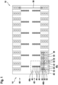
- Fig. 1 shows a top view on a power semiconductor module 10
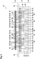
- Fig. 2 shows a cross-sectional view of the power semiconductor module 10, on which a gate driver board 12 has been attached.
- the module 10 is composed of the gate driver board 12, which is attached to an adapter board 14, which is attached to a semiconductor board 16.
- the semiconductor board 16 may comprise a substrate 18 with one or more metallization layers 20, 22, such as a DBC (direct bonded copper) substrate or an IMS (insulated metal substrate).
- the metallization layer 20 may be structured into areas 20a, 20b, 20c, which are galvanically isolated from each other with respect to the semiconductor board 16.
- a semiconductor chip 24 is bonded with a first power electrode 26.
- the opposite side of each of the semiconductor chips 24 provides a second power electrode 28 and a control electrode 30.
- the semiconductor chips 24 may be Si and/or SiC devices, such as transistors and/or thyristors.
- one or more sensors 32 are incorporated and/or attached to a semiconductor chip 24, which, for example, may sense a temperature of the semiconductor chip 24 and/or a current through the semiconductor chip 24.
- a sensor 32 may provide a contact area 33 facing the adapter board 14.
- the electrodes 28, 30 and parts of the areas 20a, 20b, 20c not covered by a chip 24 also may be seen as contact areas facing the adapter board 14.
- the one or more sensors 32 may be onboard sensors of the respective semiconductor chip 24, i.e. may be integrated into the respective semiconductor chip 24.
- the adapter board 14 which may be a printed circuit board, such as a metal-core PCB and/or flexible PCB, comprises electrically conducting vertical posts 34, 36, 38, 40 on a side facing the semiconductor board 16.
- the posts 34, 36, 38, 40 may electrically interconnect the adapter board 14 with contact areas 28, 30, 33 of the semiconductor board 16.
- the adapter board 14 comprises power terminals 42 and auxiliary terminals 44.
- the terminals 42, 44 are arranged in terminal areas 46, which are arranged above the respective semiconductor chip 24.
- terminal areas 46 which are arranged above the respective semiconductor chip 24.
- Fig. 1 only one terminal area 46 and the terminals within are depicted. However, it is shown that the module 10 has two rows 48 of terminal areas 46.
- one power terminal 42 may be electrically connected via one or more posts 34 with the respective area 20a, 20b, 20c and the corresponding power electrode 26.
- One power terminal 42 may be electrically connected via one or more posts 36 directly with the other power electrode 28.
- An auxiliary terminal 44 may be electrically connected via the post 38 directly with the control electrode 30.
- An auxiliary terminal 44 may be electrically connected via the post 40 directly with the sensor 32. It also may be that an auxiliary terminal 44 is connected via the adapter board 14 with one of the power electrodes 28, 30.
- the semiconductor chips 24 may be interconnected into different topologies with connectors 50 interconnecting the power terminals 42 of different semiconductor chips 24.
- the power terminals 42 comprise plug connectors 52 and that the connectors 50 are jumper connectors that may be plugged into these plug connectors 52. It also may be that additional connectors 50 are bridges, which are bonded with their ends to the power terminals 42. With the connectors 50, the semiconductor chips inside the module 10 may be interconnected into different topologies, such as in series, in parallel, into half-bridges, etc.
- Each terminal area 46 may be divided into an inner region 46a, in which the auxiliary terminals 44 are arranged, an intermediate region 46b, in which an inner part of the power terminals 42 is arranged and an outer region 46c, in which an outer part of the power terminals 42 is arranged.
- the outer region 46c may be provided at a border of the adapter board 14 and the outer part of the terminals 42 (and optionally the plug connectors 52 in this outer part) may be used for connecting the module terminal 54 with the power terminals 42 (see Fig. 2 ).
- the inner part of the terminals 42 (and optionally the plug connectors 52 in this part) in the intermediate region 46b, between the outer region 46c and the inner region 46a, may be used for interconnecting semiconductor chips 24 with each other.
- the gate driver board 12 may be connected with the auxiliary terminals 44.
- the auxiliary terminals may comprise press-fit plugs, into which pins 56 protruding from the gate driver board 12 may be plugged.
- the pins 56 analogously to the vertical posts 34, 36, 38, 40, may be aligned vertically with respect to the boards 12, 14, 16 and/or may protrude from a side of the gate driver board 12 facing the adapter board 14.
- the gate driver board 12 may comprise gate driver components 58, such as control components, components for evaluating sensor signals and/or passive elements, such as capacitors and resistors.
- the gate driver board 12 may be smaller as the adapter board 14 and/or solely may cover the adapter board 14 in the inner regions 46a and the intermediate regions 46b of the terminal areas 46.
- Fig. 2 also shows that the adapter board 14 and the semiconductor board 16 may be mechanically interconnected with each other via a housing 60, which may be glued to the adapter board 14 and the semiconductor board 16.
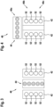
- Fig. 3 and 4 show possibilities of different terminal areas 46.
- the plug connectors 52 of the power terminals 42 may be arranged in two parallel rows.
- the auxiliary terminals 44 may be arranged in one row, which may be parallel to the power terminals 42.
- the auxiliary terminals 44 may be arranged besides both power terminals 42.
- the auxiliary terminals 44 also may be arranged between the power terminals.
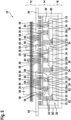
- Fig. 5 shows that the gate driver board 12 may have a press-fit pin array with pins 56, which may be pressed into the auxiliary terminals 44 designed as press-fit plugs.
- the vertical posts 34, 36, 38, 40 may be pins, which are pressed against the contact areas 28, 30, 33.
- Such pins 34, 36, 38, 40 may have a head and/or cap 62 adapted for being sintered to the respective contact area 28, 30, 33.
- the pins 34, 36, 38, 40 may be made of Cu with a sinter cap made of Ag.
- the interior of the module 10 between the adapter board 14, the semiconductor board 16 and the housing 60 may be filled with a gel and/or potted with a resin.
- the module of Fig. 5 may be manufactured by firstly pick and place the chips 24 on the substrate 18 and then sinter them to the metallization layer 20. After that, the adapter board 14 may be aligned and the pins 34, 36, 38, 40 may be sintered. After that, the module may be encapsulated. In the end, for example a customer of the module 10 may press in jumper connectors 50 and the gate driver board 12. This manufacturing may have the benefit that no embedding and/or wafer level processing may be needed.
- Fig. 6 shows a power semiconductor module 10, in which the semiconductor board 16 comprises a chip-scale package 64 for each semiconductor chip 24.
- the chip-scale packages 64 may be bonded to a substrate 18 with a structured metallization layer 20.
- Each chip-scale package 64 may comprise one or more of the semiconductor chips 24, the vertical posts (such as electroplated Cu vias and/or redistribution layers) 34, 36, 38, 40 connected to the semiconductor chips 24, and a mold and/or PCB encapsulation 66 into which the semiconductor chip 24 and the vertical posts 34, 36, 38, 40 are embedded.
- Each chip-scale package also may comprise a leadframe and/or baseplate 65 for bonding the chip package to the substrate 18 of the module 10.
- each chip-scale package 64 may provide bond areas 68, to which the vertical posts 34, 36, 38, 40 are electrically connected.
- the adapter board 14 then may be bonded to the bond areas 68 of the chip packages 64.
- each chip-scale package 64 a reverse conducting IGBT with onboard temperature and current sensor, an IGBT with freewheeling diode, or two parallel SiC MOSFETs may be accommodated.
- the module of Fig. 6 may be manufactured by firstly pick and place the chip-scale packages 64 on the substrate 18 and then bond them to the metallization layer 20. After that, the adapter board 14 may be aligned and bonded to the bond areas. In the end, for example a customer of the module 10 may press in jumper connectors 50 and the gate driver board 12. This manufacturing may have the benefit that no precision issues with respect to aligning the boards may be present and no further encapsulation may be necessary.
- Fig. 7 shows a power semiconductor module 10 in which the adapter board 14 and the semiconductor board 16 are provided by a multilayer circuit board 70, in which the at least two semiconductor chips 24 are embedded.
- the multilayer circuit board 70 may be made of a metal baseplate 22 and a lead frame 72, on which the semiconductor chips 24 are bonded. Polymer insulation layers may be arranged between the metal layers 22, 72.
- the vertical posts 34, 36, 38, 40 may be provided by through-vias and metallization tracks of the multilayer circuit board 70.
- the module of Fig. 7 may be manufactured by pick and place the semiconductor chips 24 in leadframe 72 and sinter them to the leadframe 72.
- PCB laminate layers may be arranged between the metal layers 22, 72 and the metal layers of the adapter board 14 as well as the other components, such as the through-vias 34, 36, 38, 40, the terminals 42, 44, etc. may be included and all may be laminated together.
- a customer of the module 10 may press in jumper connectors 50 and the gate driver board 12. This manufacturing may have the benefit that the module may have a rather small height and that only a low number of bonding steps and manufacturing steps at all may be necessary.
- an additional substrate 18 may not be needed.
Landscapes
- Engineering & Computer Science (AREA)
- Microelectronics & Electronic Packaging (AREA)
- Power Conversion In General (AREA)
- Combinations Of Printed Boards (AREA)
- Physics & Mathematics (AREA)
- Geometry (AREA)
- Semiconductor Integrated Circuits (AREA)
Claims (14)
- Module semi-conducteur de puissance (10), comprenant :au moins une carte semi-conductrice (16) comprenant au moins deux puces semi-conductrices (24), chaque puce semi-conductrice (24) ayant deux électrodes de puissance (26, 28) ;une carte d'adaptation (14) fixée à la carte semi-conductrice (16) au-dessus des au moins deux puces semi-conductrices (24), la carte d'adaptation (14) comprenant une zone de borne (46) pour chaque puce semi-conductrice (24) sur un côté opposé à la carte semi-conductrice (16) ;dans lequel la carte d'adaptation (14), dans chaque zone de borne (46), fournit une borne d'alimentation (42) pour chaque électrode d'alimentation (26, 28) de la puce semi-conductrice (24) associée à la zone de borne (46) ;dans lequel chaque borne d'alimentation (42) est reliée électriquement à la puce semi-conductrice (24) par l'intermédiaire d'une broche verticale (34, 36) conductrice d'électricité située sous la zone de borne (46) ;caractérisé par le fait que chaque borne d'alimentation (42) possède au moins deux connecteurs (52) ;dans lequel la carte d'adaptation (14) comprend des connecteurs de pontage (50) pour interconnecter deux connecteurs (52) pour connecter électriquement les électrodes de puissance (26, 28) de différentes puces semi-conductrices (24).
- Module semi-conducteur de puissance (10) selon la revendication 1,
dans lequel la carte d'adaptation (14) fournit au moins une borne auxiliaire (44) dans la zone de borne (46) d'au moins une des puces semi-conductrices (24) associées à la zone de borne (46), laquelle borne auxiliaire (44) est connectée à une broche verticale électriquement conductrice (38, 40) en dessous de la zone de borne (46). - Module semi-conducteur de puissance (10) selon la revendication 2,
dans lequel au moins une des puces semi-conductrices (24) associées à la zone de borne (46) comprend une électrode de commande (30) et l'une des bornes auxiliaires (44) est connectée électriquement avec sa broche verticale électriquement conductrice (38) à l'électrode de commande (30) de la puce semi-conductrice (24). - Module semi-conducteur de puissance (10) selon la revendication 2 ou la revendication 3,
dans lequel la carte semi-conductrice (16) comprend un capteur (32) pour au moins une des puces semi-conductrices (24) associées à la zone de borne (46) ; dans lequel une borne auxiliaire (44) est connectée électriquement au capteur (32) par l'intermédiaire de sa broche verticale électriquement conductrice (40). - Module semi-conducteur de puissance (10) selon la revendication 4,
dans lequel le capteur (32) est l'un parmi un capteur de température et un capteur de courant. - Module semi-conducteur de puissance (10) selon l'une quelconque des revendications 2 à 5,
dans lequel une borne auxiliaire (44) est connectée électriquement par l'intermédiaire d'une broche verticale électriquement conductrice (34, 36) à une électrode de puissance (26, 28) d'au moins une des puces semi-conductrices (24) associées à la zone de borne (46). - Module semi-conducteur de puissance (10) selon l'une quelconque des revendications précédentes,
dans lequel une borne de puissance (42) est disposée dans une région extérieure (46c) de la zone terminale respective (46), la région extérieure (46c) étant disposée sur un bord de la carte d'adaptation (14). - Module semi-conducteur de puissance (10) selon la revendication 7,
dans lequel au moins une borne auxiliaire (44) est disposée dans une région intérieure (46a) de la zone de borne (46), la région extérieure (46c) étant disposée entre le bord de la carte d'adaptation (14) et la région intérieure (46a). - Module semi-conducteur de puissance (10) selon l'une quelconque des revendications précédentes,
dans lequel les zones terminales (46) sont disposées en au moins une rangée (48) sur la carte d'adaptation (14). - Module semi-conducteur de puissance (10) selon l'une quelconque des revendications précédentes,
dans lequel la carte semi-conductrice (16) comprend un substrat (18) avec une couche de métallisation structurée (20) sur laquelle sont collées les au moins deux puces semi-conductrices (24). - Module semi-conducteur de puissance (10) selon la revendication 10,
dans lequel les broches verticales (34, 36) sont des broches, qui sont connectées à la carte d'adaptation (14) et pressées sur les zones de contact (28, 30, 33) fournies par la carte semi-conductrice (16) et les au moins deux puces semi-conductrices (24), de telle sorte que la tête de chaque broche soit collée à la zone de contact respective (28, 30, 33) de la carte semi-conductrice (16) et des au moins deux puces semi-conductrices (24). - Module semi-conducteur de puissance (10) selon l'une quelconque des revendications 1 à 9,dans lequel la carte semi-conductrice (16) comprend un boîtier de puce (64) pour chaque puce semi-conductrice (24) ;dans lequel chaque boîtier de puce (64) comprend au moins une puce semi-conductrice (24), les broches verticales (34, 36) connectées à la puce semi-conductrice (24), et une encapsulation de moule (66) dans lequel la puce semi-conductrice (24) et les broches verticales (34, 36) sont encastrées ;dans lequel chaque boîtier de puce (64) comporte des zones de liaison (68) auxquelles les broches verticales (34, 36) sont électriquement connectées ;dans lequel la carte d'adaptation (14) est collée aux zones de liaison (68) des boîtiers de puce (64).
- Module semi-conducteur de puissance (10) selon l'une quelconque des revendications 1 à 9,
dans lequel la carte d'adaptation (14) et la carte semi-conductrice (16) sont fournies par une carte de circuit imprimé multicouche (70), au niveau de laquelle les au moins deux puces semi-conductrices (24) sont intégrées ; dans lequel les broches verticales (34, 36) sont des orifices traversants de la carte de circuit imprimé multicouche (70). - Module semi-conducteur de puissance (10) selon l'une des revendications précédentes, comprenant en outre :une carte de commande de grille (12) fixée à la carte d'adaptation (14), dans laquelle des broches verticales (56) relient la carte de commande de grille (12) aux bornes auxiliaires (44) de la carte d'adaptation (14) ;dans laquelle la carte de commande de porte (12) couvre uniquement une partie des bornes d'alimentation (42) de la zone de borne (46).
Applications Claiming Priority (2)
| Application Number | Priority Date | Filing Date | Title |
|---|---|---|---|
| EP20154510 | 2020-01-30 | ||
| PCT/EP2021/052004 WO2021152021A1 (fr) | 2020-01-30 | 2021-01-28 | Module semi-conducteur de puissance configurable libre |
Publications (2)
| Publication Number | Publication Date |
|---|---|
| EP4097761A1 EP4097761A1 (fr) | 2022-12-07 |
| EP4097761B1 true EP4097761B1 (fr) | 2024-06-26 |
Family
ID=69423064
Family Applications (1)
| Application Number | Title | Priority Date | Filing Date |
|---|---|---|---|
| EP21701349.9A Active EP4097761B1 (fr) | 2020-01-30 | 2021-01-28 | Module semi-conducteur de puissance configurable librement |
Country Status (5)
| Country | Link |
|---|---|
| US (1) | US12599012B2 (fr) |
| EP (1) | EP4097761B1 (fr) |
| JP (1) | JP7684320B2 (fr) |
| CN (1) | CN115039222B (fr) |
| WO (1) | WO2021152021A1 (fr) |
Families Citing this family (12)
| Publication number | Priority date | Publication date | Assignee | Title |
|---|---|---|---|---|
| DE102021208772B4 (de) | 2021-08-11 | 2024-05-16 | Zf Friedrichshafen Ag | Halbbrücke für einen Inverter zum Betreiben eines Elektrofahrzeugantriebs, Leistungsmodul umfassend mehrere Halbbrücken, Inverter, Verfahren zum Herstellen eines Inverters |
| DE102021208767A1 (de) | 2021-08-11 | 2023-02-16 | Zf Friedrichshafen Ag | Halbbrücke für einen Inverter zum Betreiben eines Elektrofahrzeugantriebs, Leistungsmodul umfassend mehrere Halbbrücken, Inverter, Verfahren zum Herstellen eines Inverters |
| DE102021208770A1 (de) | 2021-08-11 | 2023-02-16 | Zf Friedrichshafen Ag | Halbbrücke für einen Inverter zum Betreiben eines Elektrofahrzeugantriebs, Leistungsmodul umfassend mehrere Halbbrücken, Inverter, Verfahren zum Herstellen eines Inverters |
| DE102022209564A1 (de) | 2022-09-13 | 2023-07-06 | Zf Friedrichshafen Ag | Leistungsmodul und verfahren zum montieren eines leistungsmoduls |
| DE102022211926A1 (de) * | 2022-11-10 | 2024-05-16 | D + L Dubois + Linke Gesellschaft mit beschränkter Haftung | Schweißgerät |
| DE102022213006A1 (de) * | 2022-12-02 | 2024-06-13 | Zf Friedrichshafen Ag | Leistungsmodul für einen Wandler mit separater Leiterplatte zur Steuersignalführung |
| CN119181675A (zh) * | 2023-06-21 | 2024-12-24 | 北京大学 | 半导体封装结构 |
| US12556090B2 (en) * | 2023-07-18 | 2026-02-17 | Volkswagen Aktiengesellschaft | Wide band gap (WBG) devices based three-level neutral point clamped (NPC) power module designs |
| US20250294697A1 (en) * | 2024-03-18 | 2025-09-18 | Mahle International Gmbh | Electric power converter |
| DE102024127473A1 (de) * | 2024-09-23 | 2026-03-26 | Infineon Technologies Ag | Halbleitervorrichtungen und Verfahren zu deren Herstellung |
| CN120769416B (zh) * | 2025-09-03 | 2026-01-02 | 乐山希尔电子股份有限公司 | 一种层叠式功率模块及制备方法 |
| CN121215647A (zh) * | 2025-11-27 | 2025-12-26 | 华侨大学 | 一种三相低压mosfet封装集成功率模块 |
Family Cites Families (16)
| Publication number | Priority date | Publication date | Assignee | Title |
|---|---|---|---|---|
| JP2005243713A (ja) | 2004-02-24 | 2005-09-08 | Toshiba Corp | パワーモジュール及び実装基板 |
| US8124429B2 (en) * | 2006-12-15 | 2012-02-28 | Richard Norman | Reprogrammable circuit board with alignment-insensitive support for multiple component contact types |
| DE102008033410B4 (de) * | 2008-07-16 | 2011-06-30 | SEMIKRON Elektronik GmbH & Co. KG, 90431 | Leistungselektronische Verbindungseinrichtung mit einem Leistungshalbleiterbauelement und Herstellungsverfahren hierzu |
| DE102009046258B3 (de) | 2009-10-30 | 2011-07-07 | Infineon Technologies AG, 85579 | Leistungshalbleitermodul und Verfahren zum Betrieb eines Leistungshalbleitermoduls |
| JP5551920B2 (ja) | 2009-11-24 | 2014-07-16 | イビデン株式会社 | 半導体装置及びその製造方法 |
| CN102664177B (zh) * | 2012-05-16 | 2014-10-29 | 中国科学院电工研究所 | 一种双面冷却的功率半导体模块 |
| WO2014185050A1 (fr) | 2013-05-16 | 2014-11-20 | 富士電機株式会社 | Dispositif à semi-conducteur |
| EP2871765A1 (fr) | 2013-11-08 | 2015-05-13 | Vincotech GmbH | Convertisseur NPC destiné à être utilisé dans un module de puissance et ledit module incorporant celui-ci |
| WO2015159751A1 (fr) | 2014-04-14 | 2015-10-22 | 富士電機株式会社 | Dispositif à semi-conducteur |
| JP6701641B2 (ja) | 2015-08-13 | 2020-05-27 | 富士電機株式会社 | 半導体モジュール |
| US9839146B2 (en) | 2015-10-20 | 2017-12-05 | Cree, Inc. | High voltage power module |
| JP2018073923A (ja) | 2016-10-27 | 2018-05-10 | 三菱電機株式会社 | 電力用半導体装置、電力用半導体装置の製造方法および電力変換装置 |
| EP3555914B1 (fr) | 2016-12-16 | 2021-02-03 | ABB Schweiz AG | Module semi-conducteur de puissance ayant un trajet de grille de faible inductance. |
| CN106887955A (zh) * | 2017-04-17 | 2017-06-23 | 中车青岛四方车辆研究所有限公司 | 高压大功率dc/dc模块 |
| JP2019096508A (ja) | 2017-11-24 | 2019-06-20 | 川崎重工業株式会社 | 筐体 |
| WO2021151949A1 (fr) | 2020-01-30 | 2021-08-05 | Abb Power Grids Switzerland Ag | Module semi-conducteur de puissance comportant des pinces métalliques accessibles |
-
2021
- 2021-01-28 EP EP21701349.9A patent/EP4097761B1/fr active Active
- 2021-01-28 US US17/795,970 patent/US12599012B2/en active Active
- 2021-01-28 JP JP2022546497A patent/JP7684320B2/ja active Active
- 2021-01-28 WO PCT/EP2021/052004 patent/WO2021152021A1/fr not_active Ceased
- 2021-01-28 CN CN202180011873.0A patent/CN115039222B/zh active Active
Also Published As
| Publication number | Publication date |
|---|---|
| CN115039222B (zh) | 2024-10-11 |
| WO2021152021A1 (fr) | 2021-08-05 |
| JP7684320B2 (ja) | 2025-05-27 |
| JP2023512274A (ja) | 2023-03-24 |
| US12599012B2 (en) | 2026-04-07 |
| US20230116118A1 (en) | 2023-04-13 |
| CN115039222A (zh) | 2022-09-09 |
| EP4097761A1 (fr) | 2022-12-07 |
Similar Documents
| Publication | Publication Date | Title |
|---|---|---|
| EP4097761B1 (fr) | Module semi-conducteur de puissance configurable librement | |
| US10636732B2 (en) | Power module based on multi-layer circuit board | |
| US9147585B2 (en) | Method for fabricating a plurality of semiconductor devices | |
| US9147649B2 (en) | Multi-chip module | |
| US8018056B2 (en) | Package for high power density devices | |
| US7829989B2 (en) | Vertical packaged IC device modules with interconnected 3D laminates directly contacts wafer backside | |
| US9698143B2 (en) | Wireless module with active devices | |
| CN104517952B (zh) | 功率半导体模块和用于制造功率半导体模块的方法 | |
| US10777491B2 (en) | Package comprising carrier with chip and component mounted via opening | |
| US9129960B2 (en) | Semiconductor device and manufacturing method thereof | |
| CN112368830A (zh) | 电力组件、功率模块、用于制造功率模块和电力组件的方法 | |
| US7466020B2 (en) | Power module | |
| US9490199B2 (en) | Interposer with programmable matrix for realizing configurable vertical semiconductor package arrangements | |
| US9721928B1 (en) | Integrated circuit package having two substrates | |
| CN119678253A (zh) | 用于功率封装件的积层基板 | |
| CN120237011A (zh) | 功率开关半导体器件以及将至少一个功率开关半导体器件管芯封装在封装件中的方法 |
Legal Events
| Date | Code | Title | Description |
|---|---|---|---|
| STAA | Information on the status of an ep patent application or granted ep patent |
Free format text: STATUS: UNKNOWN |
|
| STAA | Information on the status of an ep patent application or granted ep patent |
Free format text: STATUS: THE INTERNATIONAL PUBLICATION HAS BEEN MADE |
|
| PUAI | Public reference made under article 153(3) epc to a published international application that has entered the european phase |
Free format text: ORIGINAL CODE: 0009012 |
|
| STAA | Information on the status of an ep patent application or granted ep patent |
Free format text: STATUS: REQUEST FOR EXAMINATION WAS MADE |
|
| 17P | Request for examination filed |
Effective date: 20220719 |
|
| AK | Designated contracting states |
Kind code of ref document: A1 Designated state(s): AL AT BE BG CH CY CZ DE DK EE ES FI FR GB GR HR HU IE IS IT LI LT LU LV MC MK MT NL NO PL PT RO RS SE SI SK SM TR |
|
| DAV | Request for validation of the european patent (deleted) | ||
| DAX | Request for extension of the european patent (deleted) | ||
| P01 | Opt-out of the competence of the unified patent court (upc) registered |
Effective date: 20230527 |
|
| RAP1 | Party data changed (applicant data changed or rights of an application transferred) |
Owner name: HITACHI ENERGY LTD |
|
| GRAP | Despatch of communication of intention to grant a patent |
Free format text: ORIGINAL CODE: EPIDOSNIGR1 |
|
| STAA | Information on the status of an ep patent application or granted ep patent |
Free format text: STATUS: GRANT OF PATENT IS INTENDED |
|
| INTG | Intention to grant announced |
Effective date: 20240119 |
|
| RIC1 | Information provided on ipc code assigned before grant |
Ipc: H05K 3/22 20060101ALN20240105BHEP Ipc: H05K 1/02 20060101ALN20240105BHEP Ipc: H01L 23/00 20060101ALN20240105BHEP Ipc: H05K 1/14 20060101ALI20240105BHEP Ipc: H01L 25/16 20060101ALI20240105BHEP Ipc: H01L 25/07 20060101ALI20240105BHEP Ipc: H01L 23/373 20060101ALI20240105BHEP Ipc: H01L 23/498 20060101ALI20240105BHEP Ipc: H01L 23/538 20060101AFI20240105BHEP |
|
| GRAS | Grant fee paid |
Free format text: ORIGINAL CODE: EPIDOSNIGR3 |
|
| GRAA | (expected) grant |
Free format text: ORIGINAL CODE: 0009210 |
|
| STAA | Information on the status of an ep patent application or granted ep patent |
Free format text: STATUS: THE PATENT HAS BEEN GRANTED |
|
| AK | Designated contracting states |
Kind code of ref document: B1 Designated state(s): AL AT BE BG CH CY CZ DE DK EE ES FI FR GB GR HR HU IE IS IT LI LT LU LV MC MK MT NL NO PL PT RO RS SE SI SK SM TR |
|
| REG | Reference to a national code |
Ref country code: GB Ref legal event code: FG4D |
|
| REG | Reference to a national code |
Ref country code: CH Ref legal event code: EP |
|
| REG | Reference to a national code |
Ref country code: DE Ref legal event code: R096 Ref document number: 602021014808 Country of ref document: DE |
|
| PG25 | Lapsed in a contracting state [announced via postgrant information from national office to epo] |
Ref country code: BG Free format text: LAPSE BECAUSE OF FAILURE TO SUBMIT A TRANSLATION OF THE DESCRIPTION OR TO PAY THE FEE WITHIN THE PRESCRIBED TIME-LIMIT Effective date: 20240626 |
|
| PG25 | Lapsed in a contracting state [announced via postgrant information from national office to epo] |
Ref country code: FI Free format text: LAPSE BECAUSE OF FAILURE TO SUBMIT A TRANSLATION OF THE DESCRIPTION OR TO PAY THE FEE WITHIN THE PRESCRIBED TIME-LIMIT Effective date: 20240626 Ref country code: HR Free format text: LAPSE BECAUSE OF FAILURE TO SUBMIT A TRANSLATION OF THE DESCRIPTION OR TO PAY THE FEE WITHIN THE PRESCRIBED TIME-LIMIT Effective date: 20240626 |
|
| REG | Reference to a national code |
Ref country code: LT Ref legal event code: MG9D |
|
| PG25 | Lapsed in a contracting state [announced via postgrant information from national office to epo] |
Ref country code: GR Free format text: LAPSE BECAUSE OF FAILURE TO SUBMIT A TRANSLATION OF THE DESCRIPTION OR TO PAY THE FEE WITHIN THE PRESCRIBED TIME-LIMIT Effective date: 20240927 |
|
| PG25 | Lapsed in a contracting state [announced via postgrant information from national office to epo] |
Ref country code: LV Free format text: LAPSE BECAUSE OF FAILURE TO SUBMIT A TRANSLATION OF THE DESCRIPTION OR TO PAY THE FEE WITHIN THE PRESCRIBED TIME-LIMIT Effective date: 20240626 |
|
| REG | Reference to a national code |
Ref country code: NL Ref legal event code: MP Effective date: 20240626 |
|
| PG25 | Lapsed in a contracting state [announced via postgrant information from national office to epo] |
Ref country code: NO Free format text: LAPSE BECAUSE OF FAILURE TO SUBMIT A TRANSLATION OF THE DESCRIPTION OR TO PAY THE FEE WITHIN THE PRESCRIBED TIME-LIMIT Effective date: 20240926 Ref country code: LV Free format text: LAPSE BECAUSE OF FAILURE TO SUBMIT A TRANSLATION OF THE DESCRIPTION OR TO PAY THE FEE WITHIN THE PRESCRIBED TIME-LIMIT Effective date: 20240626 Ref country code: HR Free format text: LAPSE BECAUSE OF FAILURE TO SUBMIT A TRANSLATION OF THE DESCRIPTION OR TO PAY THE FEE WITHIN THE PRESCRIBED TIME-LIMIT Effective date: 20240626 Ref country code: GR Free format text: LAPSE BECAUSE OF FAILURE TO SUBMIT A TRANSLATION OF THE DESCRIPTION OR TO PAY THE FEE WITHIN THE PRESCRIBED TIME-LIMIT Effective date: 20240927 Ref country code: FI Free format text: LAPSE BECAUSE OF FAILURE TO SUBMIT A TRANSLATION OF THE DESCRIPTION OR TO PAY THE FEE WITHIN THE PRESCRIBED TIME-LIMIT Effective date: 20240626 Ref country code: BG Free format text: LAPSE BECAUSE OF FAILURE TO SUBMIT A TRANSLATION OF THE DESCRIPTION OR TO PAY THE FEE WITHIN THE PRESCRIBED TIME-LIMIT Effective date: 20240626 Ref country code: RS Free format text: LAPSE BECAUSE OF FAILURE TO SUBMIT A TRANSLATION OF THE DESCRIPTION OR TO PAY THE FEE WITHIN THE PRESCRIBED TIME-LIMIT Effective date: 20240926 |
|
| PG25 | Lapsed in a contracting state [announced via postgrant information from national office to epo] |
Ref country code: NL Free format text: LAPSE BECAUSE OF FAILURE TO SUBMIT A TRANSLATION OF THE DESCRIPTION OR TO PAY THE FEE WITHIN THE PRESCRIBED TIME-LIMIT Effective date: 20240626 |
|
| REG | Reference to a national code |
Ref country code: AT Ref legal event code: MK05 Ref document number: 1698444 Country of ref document: AT Kind code of ref document: T Effective date: 20240626 |
|
| PG25 | Lapsed in a contracting state [announced via postgrant information from national office to epo] |
Ref country code: NL Free format text: LAPSE BECAUSE OF FAILURE TO SUBMIT A TRANSLATION OF THE DESCRIPTION OR TO PAY THE FEE WITHIN THE PRESCRIBED TIME-LIMIT Effective date: 20240626 |
|
| PG25 | Lapsed in a contracting state [announced via postgrant information from national office to epo] |
Ref country code: PT Free format text: LAPSE BECAUSE OF FAILURE TO SUBMIT A TRANSLATION OF THE DESCRIPTION OR TO PAY THE FEE WITHIN THE PRESCRIBED TIME-LIMIT Effective date: 20241028 |
|
| PG25 | Lapsed in a contracting state [announced via postgrant information from national office to epo] |
Ref country code: PT Free format text: LAPSE BECAUSE OF FAILURE TO SUBMIT A TRANSLATION OF THE DESCRIPTION OR TO PAY THE FEE WITHIN THE PRESCRIBED TIME-LIMIT Effective date: 20241028 |
|
| PG25 | Lapsed in a contracting state [announced via postgrant information from national office to epo] |
Ref country code: PL Free format text: LAPSE BECAUSE OF FAILURE TO SUBMIT A TRANSLATION OF THE DESCRIPTION OR TO PAY THE FEE WITHIN THE PRESCRIBED TIME-LIMIT Effective date: 20240626 |
|
| PG25 | Lapsed in a contracting state [announced via postgrant information from national office to epo] |
Ref country code: EE Free format text: LAPSE BECAUSE OF FAILURE TO SUBMIT A TRANSLATION OF THE DESCRIPTION OR TO PAY THE FEE WITHIN THE PRESCRIBED TIME-LIMIT Effective date: 20240626 |
|
| PG25 | Lapsed in a contracting state [announced via postgrant information from national office to epo] |
Ref country code: AT Free format text: LAPSE BECAUSE OF FAILURE TO SUBMIT A TRANSLATION OF THE DESCRIPTION OR TO PAY THE FEE WITHIN THE PRESCRIBED TIME-LIMIT Effective date: 20240626 Ref country code: IS Free format text: LAPSE BECAUSE OF FAILURE TO SUBMIT A TRANSLATION OF THE DESCRIPTION OR TO PAY THE FEE WITHIN THE PRESCRIBED TIME-LIMIT Effective date: 20241026 |
|
| PG25 | Lapsed in a contracting state [announced via postgrant information from national office to epo] |
Ref country code: CZ Free format text: LAPSE BECAUSE OF FAILURE TO SUBMIT A TRANSLATION OF THE DESCRIPTION OR TO PAY THE FEE WITHIN THE PRESCRIBED TIME-LIMIT Effective date: 20240626 |
|
| PG25 | Lapsed in a contracting state [announced via postgrant information from national office to epo] |
Ref country code: RO Free format text: LAPSE BECAUSE OF FAILURE TO SUBMIT A TRANSLATION OF THE DESCRIPTION OR TO PAY THE FEE WITHIN THE PRESCRIBED TIME-LIMIT Effective date: 20240626 Ref country code: SK Free format text: LAPSE BECAUSE OF FAILURE TO SUBMIT A TRANSLATION OF THE DESCRIPTION OR TO PAY THE FEE WITHIN THE PRESCRIBED TIME-LIMIT Effective date: 20240626 |
|
| PG25 | Lapsed in a contracting state [announced via postgrant information from national office to epo] |
Ref country code: ES Free format text: LAPSE BECAUSE OF FAILURE TO SUBMIT A TRANSLATION OF THE DESCRIPTION OR TO PAY THE FEE WITHIN THE PRESCRIBED TIME-LIMIT Effective date: 20240626 Ref country code: SM Free format text: LAPSE BECAUSE OF FAILURE TO SUBMIT A TRANSLATION OF THE DESCRIPTION OR TO PAY THE FEE WITHIN THE PRESCRIBED TIME-LIMIT Effective date: 20240626 |
|
| PG25 | Lapsed in a contracting state [announced via postgrant information from national office to epo] |
Ref country code: SM Free format text: LAPSE BECAUSE OF FAILURE TO SUBMIT A TRANSLATION OF THE DESCRIPTION OR TO PAY THE FEE WITHIN THE PRESCRIBED TIME-LIMIT Effective date: 20240626 Ref country code: SK Free format text: LAPSE BECAUSE OF FAILURE TO SUBMIT A TRANSLATION OF THE DESCRIPTION OR TO PAY THE FEE WITHIN THE PRESCRIBED TIME-LIMIT Effective date: 20240626 Ref country code: RO Free format text: LAPSE BECAUSE OF FAILURE TO SUBMIT A TRANSLATION OF THE DESCRIPTION OR TO PAY THE FEE WITHIN THE PRESCRIBED TIME-LIMIT Effective date: 20240626 Ref country code: PL Free format text: LAPSE BECAUSE OF FAILURE TO SUBMIT A TRANSLATION OF THE DESCRIPTION OR TO PAY THE FEE WITHIN THE PRESCRIBED TIME-LIMIT Effective date: 20240626 Ref country code: IS Free format text: LAPSE BECAUSE OF FAILURE TO SUBMIT A TRANSLATION OF THE DESCRIPTION OR TO PAY THE FEE WITHIN THE PRESCRIBED TIME-LIMIT Effective date: 20241026 Ref country code: ES Free format text: LAPSE BECAUSE OF FAILURE TO SUBMIT A TRANSLATION OF THE DESCRIPTION OR TO PAY THE FEE WITHIN THE PRESCRIBED TIME-LIMIT Effective date: 20240626 Ref country code: EE Free format text: LAPSE BECAUSE OF FAILURE TO SUBMIT A TRANSLATION OF THE DESCRIPTION OR TO PAY THE FEE WITHIN THE PRESCRIBED TIME-LIMIT Effective date: 20240626 Ref country code: CZ Free format text: LAPSE BECAUSE OF FAILURE TO SUBMIT A TRANSLATION OF THE DESCRIPTION OR TO PAY THE FEE WITHIN THE PRESCRIBED TIME-LIMIT Effective date: 20240626 Ref country code: AT Free format text: LAPSE BECAUSE OF FAILURE TO SUBMIT A TRANSLATION OF THE DESCRIPTION OR TO PAY THE FEE WITHIN THE PRESCRIBED TIME-LIMIT Effective date: 20240626 |
|
| PG25 | Lapsed in a contracting state [announced via postgrant information from national office to epo] |
Ref country code: IT Free format text: LAPSE BECAUSE OF FAILURE TO SUBMIT A TRANSLATION OF THE DESCRIPTION OR TO PAY THE FEE WITHIN THE PRESCRIBED TIME-LIMIT Effective date: 20240626 |
|
| REG | Reference to a national code |
Ref country code: DE Ref legal event code: R097 Ref document number: 602021014808 Country of ref document: DE |
|
| PG25 | Lapsed in a contracting state [announced via postgrant information from national office to epo] |
Ref country code: DK Free format text: LAPSE BECAUSE OF FAILURE TO SUBMIT A TRANSLATION OF THE DESCRIPTION OR TO PAY THE FEE WITHIN THE PRESCRIBED TIME-LIMIT Effective date: 20240626 |
|
| PLBE | No opposition filed within time limit |
Free format text: ORIGINAL CODE: 0009261 |
|
| STAA | Information on the status of an ep patent application or granted ep patent |
Free format text: STATUS: NO OPPOSITION FILED WITHIN TIME LIMIT |
|
| 26N | No opposition filed |
Effective date: 20250327 |
|
| REG | Reference to a national code |
Ref country code: CH Ref legal event code: PL |
|
| PG25 | Lapsed in a contracting state [announced via postgrant information from national office to epo] |
Ref country code: SE Free format text: LAPSE BECAUSE OF FAILURE TO SUBMIT A TRANSLATION OF THE DESCRIPTION OR TO PAY THE FEE WITHIN THE PRESCRIBED TIME-LIMIT Effective date: 20240626 |
|
| PG25 | Lapsed in a contracting state [announced via postgrant information from national office to epo] |
Ref country code: LU Free format text: LAPSE BECAUSE OF NON-PAYMENT OF DUE FEES Effective date: 20250128 Ref country code: MC Free format text: LAPSE BECAUSE OF FAILURE TO SUBMIT A TRANSLATION OF THE DESCRIPTION OR TO PAY THE FEE WITHIN THE PRESCRIBED TIME-LIMIT Effective date: 20240626 |
|
| PG25 | Lapsed in a contracting state [announced via postgrant information from national office to epo] |
Ref country code: BE Free format text: LAPSE BECAUSE OF NON-PAYMENT OF DUE FEES Effective date: 20250131 |
|
| PG25 | Lapsed in a contracting state [announced via postgrant information from national office to epo] |
Ref country code: FR Free format text: LAPSE BECAUSE OF NON-PAYMENT OF DUE FEES Effective date: 20250131 |
|
| PG25 | Lapsed in a contracting state [announced via postgrant information from national office to epo] |
Ref country code: CH Free format text: LAPSE BECAUSE OF NON-PAYMENT OF DUE FEES Effective date: 20250131 |
|
| REG | Reference to a national code |
Ref country code: BE Ref legal event code: MM Effective date: 20250131 |
|
| REG | Reference to a national code |
Ref country code: DE Ref legal event code: R079 Ref document number: 602021014808 Country of ref document: DE Free format text: PREVIOUS MAIN CLASS: H01L0023538000 Ipc: H10W0070600000 |
|
| PG25 | Lapsed in a contracting state [announced via postgrant information from national office to epo] |
Ref country code: IE Free format text: LAPSE BECAUSE OF NON-PAYMENT OF DUE FEES Effective date: 20250128 |
|
| PGFP | Annual fee paid to national office [announced via postgrant information from national office to epo] |
Ref country code: GB Payment date: 20260123 Year of fee payment: 6 |
|
| PGFP | Annual fee paid to national office [announced via postgrant information from national office to epo] |
Ref country code: DE Payment date: 20260121 Year of fee payment: 6 |