EP4097777B1 - Dispositif électronique organique comprenant une couche d'anode, une couche de cathode, au moins une couche d'émission (eml) et au moins une couche d'injection par trous (hil) - Google Patents
Dispositif électronique organique comprenant une couche d'anode, une couche de cathode, au moins une couche d'émission (eml) et au moins une couche d'injection par trous (hil) Download PDFInfo
- Publication number
- EP4097777B1 EP4097777B1 EP21702266.4A EP21702266A EP4097777B1 EP 4097777 B1 EP4097777 B1 EP 4097777B1 EP 21702266 A EP21702266 A EP 21702266A EP 4097777 B1 EP4097777 B1 EP 4097777B1
- Authority
- EP
- European Patent Office
- Prior art keywords
- unsubstituted
- substituted
- matrix compound
- layer
- omc
- Prior art date
- Legal status (The legal status is an assumption and is not a legal conclusion. Google has not performed a legal analysis and makes no representation as to the accuracy of the status listed.)
- Active
Links
Images

Classifications
-
- H—ELECTRICITY
- H10—SEMICONDUCTOR DEVICES; ELECTRIC SOLID-STATE DEVICES NOT OTHERWISE PROVIDED FOR
- H10K—ORGANIC ELECTRIC SOLID-STATE DEVICES
- H10K85/00—Organic materials used in the body or electrodes of devices covered by this subclass
- H10K85/60—Organic compounds having low molecular weight
- H10K85/615—Polycyclic condensed aromatic hydrocarbons, e.g. anthracene
-
- H—ELECTRICITY
- H10—SEMICONDUCTOR DEVICES; ELECTRIC SOLID-STATE DEVICES NOT OTHERWISE PROVIDED FOR
- H10K—ORGANIC ELECTRIC SOLID-STATE DEVICES
- H10K85/00—Organic materials used in the body or electrodes of devices covered by this subclass
- H10K85/30—Coordination compounds
- H10K85/341—Transition metal complexes, e.g. Ru(II)polypyridine complexes
-
- H—ELECTRICITY
- H10—SEMICONDUCTOR DEVICES; ELECTRIC SOLID-STATE DEVICES NOT OTHERWISE PROVIDED FOR
- H10K—ORGANIC ELECTRIC SOLID-STATE DEVICES
- H10K50/00—Organic light-emitting devices
- H10K50/10—OLEDs or polymer light-emitting diodes [PLED]
- H10K50/11—OLEDs or polymer light-emitting diodes [PLED] characterised by the electroluminescent [EL] layers
-
- H—ELECTRICITY
- H10—SEMICONDUCTOR DEVICES; ELECTRIC SOLID-STATE DEVICES NOT OTHERWISE PROVIDED FOR
- H10K—ORGANIC ELECTRIC SOLID-STATE DEVICES
- H10K85/00—Organic materials used in the body or electrodes of devices covered by this subclass
- H10K85/30—Coordination compounds
-
- H—ELECTRICITY
- H10—SEMICONDUCTOR DEVICES; ELECTRIC SOLID-STATE DEVICES NOT OTHERWISE PROVIDED FOR
- H10K—ORGANIC ELECTRIC SOLID-STATE DEVICES
- H10K85/00—Organic materials used in the body or electrodes of devices covered by this subclass
- H10K85/30—Coordination compounds
- H10K85/371—Metal complexes comprising a group IB metal element, e.g. comprising copper, gold or silver
-
- H—ELECTRICITY
- H10—SEMICONDUCTOR DEVICES; ELECTRIC SOLID-STATE DEVICES NOT OTHERWISE PROVIDED FOR
- H10K—ORGANIC ELECTRIC SOLID-STATE DEVICES
- H10K85/00—Organic materials used in the body or electrodes of devices covered by this subclass
- H10K85/60—Organic compounds having low molecular weight
- H10K85/615—Polycyclic condensed aromatic hydrocarbons, e.g. anthracene
- H10K85/626—Polycyclic condensed aromatic hydrocarbons, e.g. anthracene containing more than one polycyclic condensed aromatic rings, e.g. bis-anthracene
-
- H—ELECTRICITY
- H10—SEMICONDUCTOR DEVICES; ELECTRIC SOLID-STATE DEVICES NOT OTHERWISE PROVIDED FOR
- H10K—ORGANIC ELECTRIC SOLID-STATE DEVICES
- H10K85/00—Organic materials used in the body or electrodes of devices covered by this subclass
- H10K85/60—Organic compounds having low molecular weight
- H10K85/649—Aromatic compounds comprising a hetero atom
- H10K85/657—Polycyclic condensed heteroaromatic hydrocarbons
- H10K85/6572—Polycyclic condensed heteroaromatic hydrocarbons comprising only nitrogen in the heteroaromatic polycondensed ring system, e.g. phenanthroline or carbazole
-
- H—ELECTRICITY
- H10—SEMICONDUCTOR DEVICES; ELECTRIC SOLID-STATE DEVICES NOT OTHERWISE PROVIDED FOR
- H10K—ORGANIC ELECTRIC SOLID-STATE DEVICES
- H10K85/00—Organic materials used in the body or electrodes of devices covered by this subclass
- H10K85/60—Organic compounds having low molecular weight
- H10K85/649—Aromatic compounds comprising a hetero atom
- H10K85/657—Polycyclic condensed heteroaromatic hydrocarbons
- H10K85/6574—Polycyclic condensed heteroaromatic hydrocarbons comprising only oxygen in the heteroaromatic polycondensed ring system, e.g. cumarine dyes
-
- H—ELECTRICITY
- H10—SEMICONDUCTOR DEVICES; ELECTRIC SOLID-STATE DEVICES NOT OTHERWISE PROVIDED FOR
- H10K—ORGANIC ELECTRIC SOLID-STATE DEVICES
- H10K85/00—Organic materials used in the body or electrodes of devices covered by this subclass
- H10K85/60—Organic compounds having low molecular weight
- H10K85/649—Aromatic compounds comprising a hetero atom
- H10K85/657—Polycyclic condensed heteroaromatic hydrocarbons
- H10K85/6576—Polycyclic condensed heteroaromatic hydrocarbons comprising only sulfur in the heteroaromatic polycondensed ring system, e.g. benzothiophene
-
- H—ELECTRICITY
- H10—SEMICONDUCTOR DEVICES; ELECTRIC SOLID-STATE DEVICES NOT OTHERWISE PROVIDED FOR
- H10K—ORGANIC ELECTRIC SOLID-STATE DEVICES
- H10K2101/00—Properties of the organic materials covered by group H10K85/00
- H10K2101/30—Highest occupied molecular orbital [HOMO], lowest unoccupied molecular orbital [LUMO] or Fermi energy values
-
- H—ELECTRICITY
- H10—SEMICONDUCTOR DEVICES; ELECTRIC SOLID-STATE DEVICES NOT OTHERWISE PROVIDED FOR
- H10K—ORGANIC ELECTRIC SOLID-STATE DEVICES
- H10K2101/00—Properties of the organic materials covered by group H10K85/00
- H10K2101/40—Interrelation of parameters between multiple constituent active layers or sublayers, e.g. HOMO values in adjacent layers
-
- H—ELECTRICITY
- H10—SEMICONDUCTOR DEVICES; ELECTRIC SOLID-STATE DEVICES NOT OTHERWISE PROVIDED FOR
- H10K—ORGANIC ELECTRIC SOLID-STATE DEVICES
- H10K50/00—Organic light-emitting devices
- H10K50/10—OLEDs or polymer light-emitting diodes [PLED]
- H10K50/17—Carrier injection layers
Definitions
- the present invention relates to an organic electronic device containing an anode layer, a cathode layer, at least one emission layer (EML) and at least one hole injection layer (HIL), wherein the hole injection layer comprises an organic matrix compound.
- EML emission layer
- HIL hole injection layer
- Organic electronic devices such as organic light-emitting diodes OLEDs, which are selfemitting devices, have a wide viewing angle, excellent contrast, quick response, high brightness, excellent operating voltage characteristics, and color reproduction.
- a typical OLED comprises an anode layer, a hole injection layer HIL, a hole transport layer HTL, an emission layer EML, an electron transport layer ETL, and a cathode layer, which are sequentially stacked on a substrate.
- the HIL, the HTL, the EML, and the ETL are thin films formed from organic compounds.
- WO2017029370 A1 relates to metal amides of general Formula Ia and for their use as hole injection layer (HIL) for an Organic light-emitting diode (OLED), and a method of manufacturing Organic light-emitting diode (OLED) comprising an hole injection layer containing a metal amide of general Formula Ia.
- hole transport layer which may comprises in addition a triarylamine compound having the Formula VIIa:
- the emission layer may be formed of a combination of a host and a dopant.
- WO2017029366 A1 relates to a hole injection layer for an OLED comprising a triarylamine compound doped with a charge neutral metal amide compound, characterized in that the hole injection layer has a thickness of at least ⁇ 20 nm to ⁇ 1000 nm and the charge neutral metal amide compound has the Formula Ia.
- a hole injection layer comprises a triarylamine compound having the Formula VIIa:
- the emission layer may be formed of a combination of a host and a dopant.
- WO2017102861 A1 relates to an organic electronic component (10) comprising at least one organic layer (3), which has a fluorinated sulphonamide metal salt of the following formula 1: (1) wherein M is either a bivalent or higher-order metal having an atomic mass of greater than 26 g/mol or a monovalent metal having an atomic mass of greater than or equal to 39 g/mol, wherein 1 ⁇ n ⁇ 7, and wherein R1, R2 are selected independently of each other and from a group comprising a fluoride-substituted aryl radical, a fluoride-substituted alkyl radical, and a fluoride-substituted aryl-alkyl radical.
- the matrix material is a hole-transport material.
- the organic electronic component comprises a light-emitting layer.
- US2016336519A1 provides a novel light-emitting element, a light-emitting element with a long lifetime, or a light-emitting element with high emission efficiency.
- the light-emitting element includes an EL layer between a pair of electrodes.
- the EL layer includes at least a light-emitting layer containing a fluorescent substance and a host material, a first electron-transport layer containing a first electron-transport material, and a second electron-transport layer containing a second electron-transport material, which are in contact with each other and in this order.
- the LUMO level of each of the host material and the second electron-transport material is higher than the LUMO level of the first electron-transport material.
- US2019198789A1 discloses an organic light emitting diode and an organic light emitting display including the same, where the organic light emitting diode includes: a first electrode; a light emitting stack disposed on the first electrode; and a second electrode disposed on the light emitting stack, where the light emitting stack includes a hole transport layer and a blue light emitting layer such that the hole transport layer and the blue light emitting layer are sequentially stacked on the first electrode, where the blue light emitting layer includes a blue host material and a blue fluorescent dopant material, and the hole transport layer includes a hole transport layer material.
- the blue fluorescent dopant material has a higher LUMO energy level than the blue host material and the blue fluorescent dopant material has a higher HOMO energy level than the blue host material.
- An aspect of the present invention provides an organic electronic device in accordance with claim 1 comprising an anode layer, a cathode layer, at least one emission layer (EML) and at least one hole injection layer (HIL), wherein the hole injection layer is arranged between the anode layer and the at least one emission layer; wherein
- EML emission layer
- HIL hole injection layer
- HOMO level is understood to mean the highest occupied molecular orbital and is determined in eV (electron Volt).
- the organic electronic device comprises an anode layer, a cathode layer, at least one emission layer (EML) and at least one hole injection layer (HIL), wherein the hole injection layer is arranged between the anode layer and the at least one emission layer;
- the organic electronic device comprises an anode layer, a cathode layer, at least one emission layer (EML) and at least one hole injection layer (HIL), wherein the hole injection layer is arranged between the anode layer and the at least one emission layer;
- the organic electronic device comprises an anode layer, a cathode layer, at least one emission layer (EML) and at least one hole injection layer (HIL), wherein the hole injection layer is arranged between the anode layer and the at least one emission layer;
- the organic electronic device comprises an anode layer, a cathode layer, at least one emission layer (EML) and at least one hole injection layer (HIL), wherein the hole injection layer is arranged between the anode layer and the at least one emission layer;
- the organic electronic device comprises an anode layer, a cathode layer, at least one emission layer (EML) and at least one hole injection layer (HIL), wherein the hole injection layer is arranged between the anode layer and the at least one emission layer;
- the organic electronic device comprises an anode layer, a cathode layer, at least one emission layer (EML) and at least one hole injection layer (HIL), wherein the hole injection layer is arranged between the anode layer and the at least one emission layer;
- the organic electronic device comprises an anode layer, a cathode layer, at least one emission layer (EML) and at least one hole injection layer (HIL), wherein the hole injection layer is arranged between the anode layer and the at least one emission layer;
- HOMO level is understood to mean the highest occupied molecular orbital and is determined in eV (electron Volt);
- HOMO level further away from vacuum level is understood to mean that the absolute value of the HOMO level is higher than the absolute value of the HOMO level of the reference compound.
- the term “further away from vacuum level than the HOMO level of N4,N4′′′-di(naphthalen-1-yl)-N4,N4′′′-diphenyl-[1,1':4',1":4",1′′′-quaterphenyl]-4,4′′′-diamine” is understood to mean that the absolute value of the HOMO level of the organic matrix compound (OMC) is higher than the HOMO level of N4,N4'"-di(naphthalen-1-yl)-N4,N4"'-diphenyl-[1,1':4',1":4",1′′′-quaterphenyl]-4,4′′′-diamine.
- the HOMO level of the emitter matrix compound (EMC) and the HOMO level of the organic matrix compound (OMC) fulfills the following equation: -0 . 2 eV ⁇ HOMO level EMC - HOMO level OMC ⁇ 0.7 eV , alternatively -0.1 eV ⁇ [HOMO level (EMC) - HOMO level (OMC)] ⁇ 0.7 eV, alternatively -0.05 eV ⁇ [HOMO level (EMC) - HOMO level (OMC)] ⁇ 0.6 eV, alternatively -0.05 eV ⁇ [HOMO level (EMC) - HOMO level (OMC)] ⁇ 0.55 eV.
- the HOMO level of the organic matrix compound (OMC) and HOMO level of the emitter matrix compound (EMC) may be calculated by quantum mechanical methods.
- the HOMO level of the organic matrix compound (OMC) and HOMO level of the emitter matrix compound (EMC) may be calculated with the program package TURBOMOLE V6.5, available from TURBOMOLE GmbH, Litzenhardtstrasse 19, 76135 Düsseldorf, Germany.
- HOMO level is calculated by this method, organic matrix compounds in the prior art have the following HOMO levels.
- HOMO levels calculated from redox potential are also provided.
- Name Structure HOMO level based on redox potential (eV) disclosed in WO2017029370 HOMO level calculated with TURBOMOL E V6.5 (eV) N,N,N',N'-Tetrakis(4-methylphenyl)-benzidine -4.99 - (T-1) N4,N4,N4',N4'-tetra(biphenyl-4-yl)biphenyl-4,4'-diamine -5.08 -4.73 (T-2) Biphenyl-4-yl(9,9-diphenyl-9H-fluoren-2-yl)-[4-(9-phenyl-9H-carbazol-3-yl)phenyl]-amine -5.10 -4.69 (T-3) N,N'-Bis(naphthalen-1-y
- the HOMO level is far away from vacuum level, accurate measurement of the redox potential may no longer be viable. Therefore, in the specification the HOMO level is determined by quantum mechanical methods, unless stated otherwise.
- the ligand L has a negative charge.
- the ligand L has one negative charge, in other words the ligand L is mono-anionic.
- the negative charge of the Ligand L may correspond to the valency of the metal ion M.
- the organic electronic device in accordance with claim 1 comprises an anode layer, a cathode layer, at least one emission layer (EML) and at least one hole injection layer (HIL), wherein the hole injection layer is arranged between the anode layer and the at least one emission layer, wherein
- EML emission layer
- HIL hole injection layer
- the organic electronic device comprising an anode layer, a cathode layer, at least one emission layer (EML) and at least one hole injection layer (HIL), wherein the hole injection layer is arranged between the anode layer and the at least one emission layer, wherein
- the organic electronic device comprising an anode layer, a cathode layer, at least one emission layer (EML) and at least one hole injection layer (HIL), wherein the hole injection layer is arranged between the anode layer and the at least one emission layer, wherein
- EML emission layer
- HIL hole injection layer
- the organic matrix compound (OMC) and the emitter matrix compound (EMC) according to Formula (I) may be a hole transport compound.
- n is an integer from 1 to 4, preferably 1 to 3, also preferred 2 or 3.
- k, m, q, r represents the number of substituents to the neighbouring Ar moiety.
- the hole injection layer is non-emissive.
- the hole injection layer and/or the organic matrix compound (OMC) and the emitter matrix compound (EMC) of Formula (I) and/or the metal complex of formula (II) are non-emissive.
- the term "essentially non-emissive" or “non-emissive” means that the contribution of the hole injection layer, the organic matrix compound (OMC) and the emitter matrix compound (EMC) of Formula (I) and/or the metal complex of formula (II) to the visible emission spectrum from an organic electronic device, such as OLED or display device, may be less than 10 %, preferably less than 5 % relative to the visible emission spectrum.
- the visible emission spectrum is an emission spectrum with a wavelength of ⁇ 380 nm to ⁇ 780 nm.
- substituted refers to one substituted with a H, deuterium, C 1 to C 12 alkyl, unsubstituted C 6 to C 18 aryl, and unsubstituted C 3 to C 18 heteroaryl.
- an aryl group with at least 6 C-ring atoms can be substituted with 1, 2, 3, 4 or 5 substituents.
- a substituted C 6 aryl group may have 1, 2, 3, 4 or 5 phenyl substituents.
- a substituted C 6 aryl group with 4 phenyl groups is an example:
- aryl substituted refers to a substitution with one or more aryl groups, which themselves may be substituted with one or more aryl and/or heteroaryl groups.
- heteroaryl substituted refers to a substitution with one or more heteroaryl groups, which themselves may be substituted with one or more aryl and/or heteroaryl groups.
- an "alkyl group” refers to a saturated aliphatic hydrocarbyl group.
- the alkyl group may be a C 1 to C 12 alkyl group. More specifically, the alkyl group may be a C 1 to C 10 alkyl group or a C 1 to C 6 alkyl group.
- a C 1 to C 4 alkyl group includes 1 to 4 carbons in alkyl chain, and may be selected from methyl, ethyl, propyl, iso-propyl, n-butyl, iso-butyl, sec-butyl, and tert-butyl.
- alkyl group may be a methyl group, an ethyl group, a propyl group, an iso-propyl group, a butyl group, an iso-butyl group, a sec-butyl group, a tert-butyl group, a pentyl group, a branched pentyl group, a hexyl group.
- cycloalkyl refers to saturated hydrocarbyl groups derived from a cycloalkane by formal abstraction of one hydrogen atom from a ring atom comprised in the corresponding cycloalkane.
- examples of the cycloalkyl group may be a cyclopropyl group, a cyclobutyl group, a cyclopentyl group, a cyclohexyl group, a methyl cyclohexyl group, an adamantly group and the like.
- hetero is understood the way that at least one carbon atom, in a structure which may be formed by covalently bound carbon atoms, is replaced by another polyvalent atom.
- the heteroatoms are selected from B, Si, N, P, O, S; more preferably from N, P, O, S.
- Preferred examples of the compounds according to Formula (I), which can be covalent bonded compounds are organic compounds that consisting predominantly from covalently bound C, H, O, N, S, which may optionally comprise also covalently bound B, P, As, Se.
- the compounds according to Formula (I), which can be a covalent compound is free of metal atoms and majority of its skeletal atoms may be selected from C, O, S, N.
- the covalent compounds according to Formula (I) are free of metal atoms and majority of its skeletal atoms may be selected from C and N.
- the organic matrix compound (OMC) and the emitter matrix compound (EMC) according to Formula (I) may comprise hetero-atom/s that are selected from the group comprising O, S, N, B, P or Si, preferably the hetero-atom is selected from the group comprising O, S, N, B or Si, alternatively the hetero-atom is selected from the group comprising O, S, N or Si.
- aryl group and “aromatic rings” refers to a hydrocarbyl group which can be created by formal abstraction of one hydrogen atom from an aromatic ring in the corresponding aromatic hydrocarbon.
- Aromatic hydrocarbon refers to a hydrocarbon which contains at least one aromatic ring or aromatic ring system.
- Aromatic ring or aromatic ring system refers to a planar ring or ring system of covalently bound carbon atoms, wherein the planar ring or ring system comprises a conjugated system of delocalized electrons fulfilling Hückel's rule.
- aryl groups include monocyclic groups like phenyl or tolyl, polycyclic groups which comprise more aromatic rings linked by single bonds, like biphenyl, and polycyclic groups comprising fused rings, like naphthyl or fluorenyl.
- heteroaryl and “heteroaromatic” it is especially where suitable understood a group derived by formal abstraction of one ring hydrogen from a heterocyclic aromatic ring in a compound comprising at least one such ring.
- non-heterocycle is understood to mean a ring or ring-system comprising no hetero-atom as a ring member.
- heterocycle is understood to mean that the heterocycle comprises at least one ring comprising one or more hetero-atoms.
- a heterocycle comprising more than one ring means that all rings comprising a hetero-atom or at least one ring comprising a hetero atom and at least one ring comprising C-atoms only and no hetero atom.
- heterocycloalkyl it is especially where suitable understood a group derived by formal abstraction of one ring hydrogen from a saturated cycloalkyl ring in a compound comprising at least one such ring.
- fused aryl rings or “condensed aryl rings” is understood the way that two aryl rings are considered fused or condensed when they share at least two common sp 2 -hybridized carbon atoms.
- fused ring system is understood to mean a ring system wherein two or more rings share at least two atoms.
- the term"5-, 6- or 7-member ring is understood to mean a ring comprising 5, 6 or 7 atoms.
- the atoms may be selected from C and one or more hetero-atoms.
- the single bond refers to a direct bond.
- adjacent to is understood to mean that distance between layers may be less than 20 nm or that the adjacent arranged layers contact each other.
- contacting sandwiched refers to an arrangement of three layers whereby the layer in the middle is in direct contact with the two adjacent layers.
- OLED organic light-emitting diode
- organic light-emitting device organic light-emitting device
- anode anode layer and anode electrode are used synonymously.
- cathode cathode layer and cathode electrode are used synonymously.
- hole injection layer is understood to mean a layer which improves charge injection from the anode layer into the at least one emission layer.
- hole transport layer is understood to mean a layer which transports holes between the hole injection layer and the at least one emission layer and/or between a first and a second emission layer.
- the operating voltage U is measured in Volt.
- hole characteristics refer to an ability to donate an electron to form a hole when an electric field is applied and that a hole formed in the anode may be easily injected into the emission layer and transported in the emission layer due to conductive characteristics according to a highest occupied molecular orbital (HOMO) level.
- HOMO highest occupied molecular orbital
- electron characteristics refer to an ability to accept an electron when an electric field is applied and that electrons formed in the cathode may be easily injected into the emission layer and transported in the emission layer due to conductive characteristics according to a lowest unoccupied molecular orbital (LUMO) level.
- LUMO lowest unoccupied molecular orbital
- the organic electronic device according to the invention solves the problem underlying the present invention by enabling organic electronic devices, such as organic light-emitting diodes, in various aspects superior over the organic electronic devices known in the art, in particular with respect to operating voltage.
- the problem underlying the present invention can be solved by providing compounds which may be suitable for deposition through vacuum thermal evaporation under conditions suitable for mass production.
- the rate onset temperature of the organic matrix compound (OMC), emitter matrix compound (EMC) and of the metal complex of the present invention may be in a range suitable for mass production.
- the HOMO level of the organic matrix compound (OMC) or organic matrix compound (OMC) of Formula (I) is further away from vacuum level than the HOMO level of N4,N4′′′-di(naphthalen-1-yl)-N4,N4′′′-diphenyl-[1,1':4',1":4",1′′′-quaterphenyl]-4,4"'-diamine (-4.85 eV calculated by the method described in the present specification) when determined under the same conditions.
- the HOMO level of the organic matrix compound (OMC) of Formula (I) is further away from vacuum level than the HOMO level of N,N'-((9H-fluorene-9,9-diyl)bis(4,1-phenylene))bis(N-([1,1'-biphenyl]-4-yl)-[1,1'-biphenyl]-4-amine) (-4.86 eV calculated by the method described in the present specification); alternatively the HOMO level of the organic matrix compound (OMC) of Formula (I) is the same or further away from vacuum level than the HOMO level of 9-phenyl-10-(3',4',5'-triphenyl-[1,1':2',1"-terphenyl]-3-yl)anthracene (-5.04 eV calculated by the method described in the present specification); alternatively, the HOMO level of the organic matrix compound (OMC) of Formula (I) is the same or further away from vacuum
- the HOMO level of the organic matrix compound (OMC) of Formula (I) is further away from vacuum level than the HOMO level of N4,N4′′′-di(naphthalen-1-yl)-N4,N4′′′-diphenyl-[1,1':4',1":4",1′′′-quaterphenyl]-4,4"'-diamine and the same or closer to vacuum level than 4,4',4"-(1,3,5-Benzenetriyl)tris-[dibenzothiophene] when determined under the same conditions; preferably the HOMO level of the organic matrix compound (OMC) of Formula (I) is further away from vacuum level than the HOMO level of N,N'-((9H-fluorene-9,9-diyl)bis(4,1-phenylene))bis(N-([1,1'-biphenyl]-4-yl)-[1,1'-biphenyl]-4-amine) and the same or closer
- HOMO level closer to vacuum level is understood to mean that the absolute value of the HOMO level is lower than the absolute value of the HOMO level of the reference compound.
- close to vacuum level than the HOMO level of 4,4',4"-(1,3,5-Benzenetriyl)tris[dibenzothiophene] is understood to mean that the absolute value of the HOMO level of the organic matrix compound (OMC) is lower than the HOMO level of 4,4',4"-(1,3,5-Benzenetriyl)tris[dibenzothiophene].
- the HOMO level of the organic matrix compound (OMC) of Formula (I) is further away from vacuum level than the HOMO level of N4,N4′′′-di(naphthalen-1-yl)-N4,N4"'-diphenyl-[1,1':4',1":4",1′′′-quaterphenyl]-4,4"'-diamine when determined under the same conditions; wherein the HOMO level of N4,N4'"-di(naphthalen-1-yl)-N4,N4′′′-diphenyl-[1,1':4',1":4",1′′′-quaterphenyl]-4,4′′′-diamine is -4.85 eV;
- the HOMO level of the organic matrix compound (OMC) of Formula (I) and/or the emitter matrix compound (EMC) of Formula (I) is further away from vacuum level than the HOMO level of N,N'-((9H-fluorene-9,9-diyl)bis(4,1-phenylene))bis(N-([1,1'-biphenyl]-4-yl)-[1,1'-biphenyl]-4-amine) (-4.86 eV calculated by the method described in the present specification).
- the HOMO level of the organic matrix compound (OMC) of Formula (I) and/or the emitter matrix compound (EMC) of Formula (I) is further away from vacuum level than the HOMO level of N4,N4′′′-di(naphthalen-1-yl)-N4,N4′′′-diphenyl-[1,1':4',1":4",1′′′-quaterphenyl]-4,4"'-diamine and the same or closer to vacuum level than 4,4',4"-(1,3,5-Benzenetriyl)tris-[dibenzothiophene] when determined under the same conditions; preferably the HOMO level of the organic matrix compound (OMC) of Formula (I) and/or the emitter matrix compound (EMC) of Formula (I) is further away from vacuum level than the HOMO level of N,N'-((9H-fluorene-9,9-diyl)bis(4,1-phenylene))bis(N-([1,1
- the HOMO level of the organic matrix compound (OMC) of Formula (I) and/or the emitter matrix compound (EMC) of Formula (I) is further away from vacuum level than the HOMO level of N4,N4′′′-di(naphthalen-1-yl)-N4,N4′′′-diphenyl-[1,1':4',1":4",1′′′-quaterphenyl]-4,4"'-diamine when determined under the same conditions; wherein the HOMO level of N4,N4'"-di(naphthalen-1-yl)-N4,N4′′′-diphenyl-[1,1':4',1":4",1′′′-quaterphenyl]-4,4′′′-diamine is -4.85 eV, preferably, the HOMO level of the organic matrix compound (OMC) of Formula (I) and/or the emitter matrix compound (EMC) of Formula (I) is further away from vacuum level than the HOMO level
- the organic matrix compound (OMC) fulfills the following equation: -7 eV ⁇ HOMO level (OMC) ⁇ -4.85 eV, alternatively -6 eV ⁇ HOMO level (OMC) ⁇ - 4.86 eV, alternatively -6 eV ⁇ HOMO level (OMC) ⁇ -4.9 eV, alternatively -6 eV ⁇ HOMO level (OMC) ⁇ -5 eV, alternatively -5.8 eV ⁇ HOMO level (OMC) ⁇ -5.05 eV, alternatively -5.7 eV ⁇ HOMO level (OMC) ⁇ -5.1 eV.
- the emitter matrix compound (EMC) fulfills the following equation: -7 eV ⁇ HOMO level (EMC) ⁇ -4.85 eV, alternatively -6 eV ⁇ HOMO level (EMC) ⁇ - 4.86 eV, alternatively -6 eV ⁇ HOMO level (EMC) ⁇ -4.9 eV, alternatively -6 eV ⁇ HOMO level (EMC) ⁇ -5 eV, alternatively -5.7 eV ⁇ HOMO level (EMC) ⁇ -5.05 eV, alternatively -5.3 eV ⁇ HOMO level (EMC) ⁇ -5.1 eV.
- the organic matrix compound (OMC) has the Formula (I): (Ar 1 ) k -(Ar 2 ) m -Ar 3 -(Ar 4 ) p -(Ar 5 ) q -(Ar 6 ) r (I), wherein
- the organic matrix compound (OMC) of Formula (I) contained in the hole injection layer and/or the emitter matrix compound (EMC) of Formula (I) contained in the emission layer (EML) may have a molecular weight Mw of ⁇ 400 and ⁇ 2000 g/mol, preferably a molecular weight Mw of ⁇ 450 and ⁇ 1500 g/mol, further preferred a molecular weight Mw of ⁇ 500 and ⁇ 1000 g/mol, in addition preferred a molecular weight Mw of ⁇ 550 and ⁇ 900 g/mol, also preferred a molecular weight Mw of ⁇ 600 and ⁇ 800 g/mol.
- the HOMO level of the organic matrix compound (OMC) of Formula (I) may be less than -4.85 eV and more than -7 eV, preferably less than -4.9 eV and more than -7 eV, alternatively less than -4.95 eV and more than -7 eV, alternatively less than -5 eV and more than -7 eV, alternatively less than -5.05 eV and more than -7 eV, alternatively less than -5.09 eV and more than -7 eV.
- the HOMO level of the organic matrix compound (OMC) of Formula (I) and/or the the emitter matrix compound (EMC) of Formula (I) may be less than -4.85 eV and more than - 7 eV, preferably less than -4.9 eV and more than -7 eV, alternatively less than -4.95 eV and more than -7 eV, alternatively less than -5 eV and more than -7 eV.
- the HOMO level of the organic matrix compound (OMC) of Formula (I) and/or the emitter matrix compound (EMC) of Formula (I) may be less than -4.85 eV and more than - 6.5 eV, preferably less than -4.9 eV and more than -6.5 eV, alternatively less than -4.95 eV and more than - 6.5 eV, alternatively less than -5 eV and more than -6.5 eV, alternatively less than - 5.05 eV and more than -6.5 eV, alternatively less than -5.09 eV and more than -6.5 eV.
- the HOMO level of the organic matrix compound (OMC) of Formula (I) and/or the emitter matrix compound (EMC) of Formula (I) may be less than -4.85 eV and more than - 6 eV, preferably less than -4.9 eV and more than -6 eV, alternatively less than -4.95 eV and more than -6 eV, alternatively less than -5 eV and more ve than -6 eV, alternatively less than -5.05 eV and more than -6 eV, alternatively less than -5.09 eV and more than -6 eV.
- the organic matrix compound (OMC) of Formula (I) and/or the emitter matrix compound (EMC) of Formula (I) may comprises at least ⁇ 1 to ⁇ 6 substituted or unsubstituted aromatic fused ring systems comprising heteroaromatic rings.
- the organic matrix compound (OMC) of Formula (I) and/or the the emitter matrix compound (EMC) of Formula (I) may comprises at least ⁇ 1 to ⁇ 6 substituted or unsubstituted aromatic fused ring systems comprising heteroaromatic rings and at least ⁇ 1 to ⁇ 3 substituted or unsubstituted unsaturated 5- to 7-member ring of a heterocycle, preferably ⁇ 2 to ⁇ 5 substituted or unsubstituted aromatic fused ring systems comprising heteroaromatic rings.
- the organic matrix compound (OMC) of Formula (I) and/or the emitter matrix compound (EMC) of Formula (I) may comprises at least ⁇ 1 to ⁇ 6 substituted or unsubstituted aromatic fused ring systems comprising heteroaromatic rings and at least ⁇ 1 to ⁇ 3 substituted or unsubstituted unsaturated 5- to 7-member ring of a heterocycle, preferably ⁇ 2 to ⁇ 5 substituted or unsubstituted aromatic fused ring systems comprising heteroaromatic rings, and at least ⁇ 1 to ⁇ 3 substituted or unsubstituted unsaturated 5- to 7-member ring of a heterocycle, further preferred 3 or 4 substituted or unsubstituted aromatic fused ring systems comprising heteroaromatic rings and optional at least ⁇ 1 to ⁇ 3 substituted or unsubstituted unsaturated 5- to 7-member ring of a heterocycle, and additional preferred wherein the aromatic fused ring systems comprising heteroaromatic rings are unsubsti
- the organic matrix compound (OMC) of Formula (I) and/or the emitter matrix compound (EMC) of Formula (I) may comprises at least ⁇ 1 to ⁇ 6 substituted or unsubstituted aromatic fused ring systems, preferably ⁇ 2 to ⁇ 5 substituted or unsubstituted aromatic fused ring systems, and further preferred 3 or 4 substituted or unsubstituted aromatic fused ring systems.
- the organic matrix compound (OMC) of Formula (I) and/or the emitter matrix compound (EMC) of Formula (I) may comprises at least ⁇ 1 to ⁇ 6 substituted or unsubstituted aromatic fused ring systems, preferably ⁇ 2 to ⁇ 5 substituted or unsubstituted aromatic fused ring systems, and further preferred 3 or 4 substituted or unsubstituted aromatic fused ring systems, which comprises substituted or unsubstituted heteroaromatic rings.
- the organic matrix compound (OMC) of Formula (I) and/or the emitter matrix compound (EMC) of Formula (I) may comprises at least ⁇ 1 to ⁇ 3 or 2 substituted or unsubstituted unsaturated 5- to 7-member ring of a heterocycle.
- the organic matrix compound (OMC) of Formula (I) and/or the emitter matrix compound (EMC) of Formula (I) may comprises at least ⁇ 1 to ⁇ 3 or 2 substituted or unsubstituted unsaturated 7-member ring of a heterocycle.
- substituted or unsubstituted aromatic fused ring systems of the organic matrix compound (OMC) of Formula (I) and/or the emitter matrix compound (EMC) of Formula (I) may comprises at least ⁇ 1 to ⁇ 3 or 2 substituted or unsubstituted unsaturated 5- to 7-member ring of a heterocycle.
- the substituted or unsubstituted aromatic fused ring systems of the organic matrix compound (OMC) of Formula (I) and/or the emitter matrix compound (EMC) of Formula (I) may comprises at least ⁇ 1 to ⁇ 3 or 2 substituted or unsubstituted unsaturated 7-member ring of a heterocycle.
- the organic matrix compound (OMC) of Formula (I) and/or the emitter matrix compound (EMC) of Formula (I) may comprises at least ⁇ 1 to ⁇ 6 substituted or unsubstituted aromatic fused ring systems, preferably ⁇ 2 to ⁇ 5 substituted or unsubstituted aromatic fused ring systems, and further preferred 3 or 4 substituted or unsubstituted aromatic fused ring systems, and wherein the aromatic fused ring system comprises substituted or unsubstituted unsaturated 5- to 7-member ring of a heterocycle.
- the organic matrix compound (OMC) of Formula (I) and/or the emitter matrix compound (EMC) of Formula (I) may comprises at least ⁇ 1 to ⁇ 6 substituted or unsubstituted aromatic fused ring systems, preferably ⁇ 2 to ⁇ 5 substituted or unsubstituted aromatic fused ring systems, and further preferred 3 or 4 substituted or unsubstituted aromatic fused ring systems, which comprises substituted or unsubstituted heteroaromatic rings, and wherein the aromatic fused ring system comprises substituted or unsubstituted unsaturated 5- to 7-member ring of a heterocycle.
- the organic matrix compound (OMC) of Formula (I) and/or the emitter matrix compound (EMC) of Formula (I) may comprises at least ⁇ 1 to ⁇ 6 substituted or unsubstituted aromatic fused ring systems, preferably ⁇ 2 to ⁇ 5 substituted or unsubstituted aromatic fused ring systems, and further preferred 3 or 4 substituted or unsubstituted aromatic fused ring systems, and wherein the aromatic fused ring system comprises at least ⁇ 1 to ⁇ 3 or 2 substituted or unsubstituted unsaturated 5- to 7-member ring of a heterocycle.
- the organic matrix compound (OMC) of Formula (I) and/or the emitter matrix compound (EMC) of Formula (I) may comprises at least ⁇ 1 to ⁇ 6 substituted or unsubstituted aromatic fused ring systems, preferably ⁇ 2 to ⁇ 5 substituted or unsubstituted aromatic fused ring systems, and further preferred 3 or 4 substituted or unsubstituted aromatic fused ring systems, which comprises substituted or unsubstituted heteroaromatic rings, and wherein the aromatic fused ring system comprises at least ⁇ 1 to ⁇ 3 or 2 substituted or unsubstituted unsaturated 5- to 7-member ring of a heterocycle.
- aromatic fused ring system may include at least one aromatic ring and at least one substituted or unsubstituted unsaturated 5- to 7- member ring. It should be noted here that the substituted or unsubstituted unsaturated 5- to 7- member ring may not be an aromatic ring.
- the organic matrix compound (OMC) of Formula (I) and/or the emitter matrix compound (EMC) of Formula (I) may comprises at least at least ⁇ 1 to ⁇ 6, preferably ⁇ 2 to ⁇ 5, or further preferred 3 or 4 of the substituted or unsubstituted aromatic fused ring systems with:
- the organic matrix compound (OMC) of Formula (I) and/or the emitter matrix compound (EMC) of Formula (I) may comprises at least at least ⁇ 1 to ⁇ 6, preferably ⁇ 2 to ⁇ 5, or further preferred 3 or 4 of the substituted or unsubstituted aromatic fused ring systems with:
- organic matrix compound (OMC) of Formula (I) and/or the emitter matrix compound (EMC) of Formula (I) may comprises:
- the organic matrix compound (OMC) of Formula (I) and/or the emitter matrix compound (EMC) of Formula (I) may comprises a hetero-atom, which may be selected from the group comprising O, S, N, B or P, preferably the hetero-atom may be selected from the group comprising O, S or N.
- the organic matrix compound (OMC) of Formula (I) and/or the emitter matrix compound (EMC) of Formula (I) may comprises at least at least ⁇ 1 to ⁇ 6, preferably ⁇ 2 to ⁇ 5, or further preferred 3 or 4 of the substituted or unsubstituted aromatic fused ring systems with:
- the organic matrix compound (OMC) of Formula (I) and/or the emitter matrix compound (EMC) of Formula (I) may be free of hetero-atoms which are not part of an aromatic ring and/or part of an unsaturated 7-member-ring, preferably the organic matrix compound (OMC) of Formula (I) and/or the emitter matrix compound (EMC) of Formula (I) may be free on N-atoms except N-atoms which are part of an aromatic ring or are part of an unsaturated 7-member-ring.
- the organic matrix compound (OMC) of Formula (I) and/or the emitter matrix compound (EMC) of Formula (I) comprises two carbazole groups, at least one dibenzofurane group, at least one dibenzothiophene group and/or at least one anthracene group.
- the organic matrix compound (OMC) of Formula (I) and/or the emitter matrix compound (EMC) of Formula (I) comprises two carbazole groups, one to three dibenzofurane groups, one to three dibenzothiophene groups and/or one to two anthracene groups.
- Ar 1 may be selected from D7 to D15 and D17.
- Ar 2 may selected from D1 to D6, or D7 to D15 and D17.
- Ar 4 may be selected from D1 to D6, or D7 to D15 and D17.
- Ar 5 may be selected from D1 to D6, or D7 to D15 and D17.
- Ar 6 may be selected from D7 to D15 and D17.
- the Ar 3 group is selected from anthracene, carbazole, dibenzothiophene and/or dibenzofurane.
- the Ar 3 group is selected anthracene.
- the Ar 3 group is selected from carbazole, dibenzothiophene and/or dibenzofurane.
- organic matrix compound (OMC) according to formula (I) and/or the emitter matrix compound (EMC) according to formula (I) may be selected from F1 to F13:
- organic matrix compound (OMC) and/or the emitter matrix compound are free of metals and/or ionic bonds.
- the hole injection layer and/or the organic matrix compound (OMC) and/or the emitter matrix compound (EMC) according to formula (I) may be free of HTM014, HTM081, HTM163, HTM222, EL-301, HTM226, HTM355, HTM133, HTM334, HTM604 and EL-22T.
- the abbreviations denote the manufacturers' names, for example, of Merck or Lumtec.
- the hole injection layer and/or the organic matrix compound (OMC) and/or the emitter matrix compound (EMC) according to formula (I) may be free of N,N'-Bis(naphthalen-1-yl)-N,N'-bis(phenyl)-9,9-dimethyl-fluorene, N,N'-Bis(3-methylphenyl)-N,N'-bis(phenyl)-9,9-dimethyl-fluorene, N,N'-Bis(naphthalen-1-yl)-N,N'-bis(phenyl)-9,9-dimethyl-fluorene, N,N'-Bis(naphthalen-1-yl)-N,N'-bis(phenyl)-2,2-dimethylbenzidine, N,N'-Bis(3-methylphenyl)-N,N'-bis(phenyl)-9,9-spirobifluorene, 2,2',7,7'-Tetrakis(N
- the metal complex according to Formula (II) may be non-emissive.
- the term "essentially non-emissive" or “non-emissive” means that the contribution of the metal complex according to Formula (II) to the visible emission spectrum from an organic electronic device, such as OLED or display device, is less than 10 %, preferably less than 5 % relative to the visible emission spectrum.
- the visible emission spectrum is an emission spectrum with a wavelength of ⁇ 380 nm to ⁇ 780 nm.
- the valency n of M is 1 or 2.
- M is selected from a metal ion wherein the corresponding metal has an electronegativity value according to Allen of less than 2.4, preferably less than 2, more preferred less than 1.9, and the valency n of M is 1 or 2.
- M is selected from an alkali, alkaline earth, rare earth or transition metal, alternatively M is selected from alkali, alkaline earth, transition or a period 4 or 5 main group metal.
- M is selected from Li, Na, K, Cs, Mg, Mn, Cu, Zn, Ag, Bi and Mo; preferably M is selected from Na, K, Cs, Mg, Mn, Cu, Zn and Ag; also preferred M is selected from Na, K, Mg, Mn, Cu, Zn and Ag, wherein if M is Cu, n is 2.
- M is a metal ion, wherein M is not Li.
- M is a metal ion, wherein M is not Li or K.
- M is a metal ion, wherein M is not Ag
- M is a metal ion, wherein M is not Cu.
- M is a metal ion, wherein M is not Mo.
- M is a metal ion, wherein M is not Ir and/or Pt.
- the metal complex according to Formula (II) may have a has a molecular weight Mw of ⁇ 287 and ⁇ 2000 g/mol, preferably a molecular weight Mw of ⁇ 400 and ⁇ 1500 g/mol, further preferred a molecular weight Mw of ⁇ 580 and ⁇ 1500 g/mol, in addition preferred a molecular weight Mw of ⁇ 580 and ⁇ 1400 g/mol.
- ligand L of Formula (II), also named L may be selected from a group comprising:
- the ligand L of Formula (II) may be selected from a group comprising at least two carbon atoms, alternatively at least three carbon atoms, at least one oxygen atom, at least two oxygen atoms, at least one oxygen and/or nitrogen atom, one nitrogen atom and at least two oxygen atoms, at least two carbon atoms and at least one oxygen atom, at least two carbon atoms and two oxygen atoms or one oxygen and one nitrogen atom, at least one or more groups selected from halogen, F, CN, substituted or unsubstituted C 1 to C 6 alkyl, substituted or unsubstituted C 1 to C 6 alkoxy, alternatively two or more groups selected from halogen, F, CN, substituted or unsubstituted C 1 to C 6 alkyl, substituted or unsubstituted C 1 to C 6 alkoxy, at least one or more groups selected from halogen, F, CN, substituted C 1 to C 6 alkyl, substituted or unsubsti
- the ligand L of Formula (II) may be selected from a group comprising F, CN, perfluorinated C 1 to C 6 alkyl, substituted or unsubstituted C 1 to C 6 alkyl, substituted or unsubstituted C 1 to C 6 alkoxy.
- the substituents may be selected from D, C 6 aryl, C 3 to C 9 heteroaryl, C 1 to C 6 alkyl, C 1 to C 6 alkoxy, C 3 to C 6 branched alkyl, C 3 to C 6 cyclic alkyl, C 3 to C 6 branched alkoxy, C 3 to C 6 cyclic alkoxy, partially or perfluorinated C 1 to C 16 alkyl, partially or perfluorinated C 1 to C 16 alkoxy, partially or perdeuterated C 1 to C 6 alkyl, partially or perdeuterated C 1 to C 6 alkoxy, COR 6 , COOR 6 , halogen, F or CN, wherein R 6 may be selected from C 6 aryl, C 3 to C 9 heteroaryl, C 1 to C 6 alkyl, C 1 to C 6 alkoxy, C 3 to C 6 branched alkyl, C 3 to C 6 cyclic alkyl, C 3 to C 6 branched alkoxy, C 3 to C 6
- the ligand L is free of sulfur atoms. According to another embodiment the ligand L is free of sulfur atoms or phthalocyanine groups.
- the ligand L of Formula (II) may be independently selected from G1 to G64, preferably G1 to G62:
- the negative charge in metal complexes of formula (II) may be delocalised partially or fully over the ligand L.
- L is selected from (G1) to (G52) and (G60) to (G64).
- L is selected from (G2) to (G59), alternatively L is selected from (G2) to (G52).
- the metal complex may be selected from the following formulas (IIa) to (IIe) and preferably be selected from the following formulas (IIa) to (IId): wherein
- the negative charge in metal complexes of formula (IIa), (IIb), (IIc) and/or (IId) may be delocalised partially or fully over the carbon and hetero atoms and A 1 , A 2 and/or A 3 .
- At least one of A 1 , A 2 and/or A 3 may comprise a substituent, wherein at least one of the substituents of A 1 , A 2 and/or A 3 may be independently selected from C 3 to C 9 heteroaryl, C 1 to C 6 alkoxy, C 3 to C 6 branched alkoxy, C 3 to C 6 cyclic alkoxy, partially or perfluorinated C 1 to C 16 alkyl, partially or perfluorinated C 1 to C 16 alkoxy, partially or perdeuterated C 1 to C 6 alkoxy, COR 1 , COOR 1 , halogen,
- At least one of A l and A 2 and/or A 3 comprises at least two substituents, wherein the substituents on A 1 , A 2 and/or A 3 may be independently selected from C 3 to C 9 heteroaryl, C 1 to C 6 alkoxy, C 3 to C 6 branched alkoxy, C 3 to C 6 cyclic alkoxy, partially or per
- a 1 , A 2 and/or A 3 may be independently selected from CF 3 , C 2 F 5 , C 3 F 7 , C 4 F 9 , C 5 F 11 , C 6 F 13 and/or phenyl substituted with two to five groups independently selected from F or CF 3 , alternatively C 2 F 5 , C 3 F 7 , C 4 F 9 , C 5 F 11 , C 6 F 13 and/or phenyl substituted with two to five groups independently selected from F or CF 3 , alternatively CF 3 , C 2 F 5 , C 3 F 7 , C 4 F 9 , C 5 F 11 , C 6 F 13 or phenyl substituted with zero to two CF 3 groups and/or zero to five F atoms.
- the metal complex may be selected from
- the metal complex may be selected from Formula (IIa) or (IIb), wherein M is selected from a metal ion wherein the corresponding metal has an electronegativity value according to Allen of less than 2.4, preferably M is selected from an alkali, alkaline earth, rare earth or transition metal, further preferred M is selected from a metal with an atomic mass ⁇ 24 Da, in addition preferred M is selected from a metal with an atomic mass ⁇ 24 Da and M has an oxidation number ⁇ 2; and/or Formula (IIc), wherein M is selected from Bi.
- M is selected from a metal ion wherein the corresponding metal has an electronegativity value according to Allen of less than 2.4
- M is selected from an alkali, alkaline earth, rare earth or transition metal
- M further preferred M is selected from a metal with an atomic mass ⁇ 24 Da
- M has an oxidation number ⁇ 2
- Formula (IIc) wherein M is selected from Bi.
- Metal complexes of the following formulas may be particularly preferred:
- the metal complex may be free of TFSI.
- the metal complex may be particularly suited to mass production of organic electronic devices.
- the hole injection layer comprises an organic matrix compound (OMC) and a metal complex, wherein the metal complex has the Formula (II): M n ⁇ (L ⁇ ) n (II), wherein
- the hole injection layer comprises an organic matrix compound (OMC) and a metal complex:
- n is an integer from 1 to 4, preferably 1 to 3, also preferred 2 or 3.
- the hole injection layer is free of ionic liquids, metal phthalocyanine, CuPc, HAT-CN, Pyrazino[2,3-f][1,10]phenanthroline-2,3-dicarbonitrile, F 4 TCNQ, metal fluoride and/or metal oxides, wherein the metal in the metal oxide is selected from Re and/or Mo.
- the hole injection layer can be deposited under conditions suitable for mass production.
- the hole injection layer is arranged in direct contact with the anode layer.
- the hole injection layer may be formed on the anode layer by vacuum deposition, spin coating, printing, casting, slot-die coating, Langmuir-Blodgett (LB) deposition, or the like.
- the deposition conditions may vary according to the organic matrix compound that is used to form the HIL, and the desired structure and thermal properties of the HIL. In general, however, conditions for vacuum deposition may include a deposition temperature of 100° C to 350° C, a pressure of 10 -8 to 10 -3 Torr (1 Torr equals 133.322 Pa), and a deposition rate of 0.1 to 10 nm/sec.
- coating conditions may vary according to the organic matrix compound that is used to form the HIL, and the desired structure and thermal properties of the HIL.
- the coating conditions may include a coating speed of 2000 rpm to 5000 rpm, and a thermal treatment temperature of 80° C to 200° C. Thermal treatment removes a solvent after the coating is performed.
- the HIL may be formed of any organic matrix compound of Formula (I) and of a metal complex of Formula (II), (IIa) to (IIe) and preferably (II), (IIa) to (IId).
- the thickness of the HIL may be in the range from 1 nm to 15 nm, and for example, from 2 nm to 12 nm, alternatively 3 nm to 10 nm.
- the HIL may have excellent hole injecting characteristics, without a substantial penalty in operating voltage.
- the hole injection layer may comprise:
- the hole injection layer may comprise:
- the hole injection layer is free of ionic liquids, metal phthalocyanine, ZnPc, CuPc, HAT-CN, Pyrazino[2,3-f][1,10]phenanthroline-2,3-dicarbonitrile, F 4 TCNQ, metal fluoride and/or metal oxides, wherein the metal in the metal oxide is selected from Re and/or Mo.
- the hole injection layer can be deposited under conditions suitable for mass production.
- the organic electronic device may comprise the hole injection layer, wherein the hole injection layer comprises a first sub-layer comprising the metal complex of Formula (II) and a second sub-layer comprising the organic matrix compound or the organic matrix compound (OMC) of Formula (I), wherein the first sub-layer is arranged closer to the anode layer and the second sub-layer is arranged closer to the at least one emission layer.
- the metal complex selected the same in both sub-layers, such as first sub-layer and second sub-layer.
- the organic electronic device may comprise the hole injection layer that comprises a first sub-layer comprising the metal complex of Formula (II) and a second sub-layer comprising the organic matrix compound (OMC) and the metal complex, wherein the first sub-layer is arranged closer to the anode layer and the second sub-layer is arranged closer to the at least one emission layer.
- the hole injection layer that comprises a first sub-layer comprising the metal complex of Formula (II) and a second sub-layer comprising the organic matrix compound (OMC) and the metal complex, wherein the first sub-layer is arranged closer to the anode layer and the second sub-layer is arranged closer to the at least one emission layer.
- the organic electronic device may comprise the hole injection layer, which comprises a first sub-layer comprising the metal complex of Formula (II) and a second sub-layer comprising the organic matrix compound (OMC) according the present invention and the metal complex according to Formula (II), wherein the first sub-layer is arranged closer to the anode layer and the second sub-layer is arranged closer to the at least one emission layer.
- the hole injection layer which comprises a first sub-layer comprising the metal complex of Formula (II) and a second sub-layer comprising the organic matrix compound (OMC) according the present invention and the metal complex according to Formula (II), wherein the first sub-layer is arranged closer to the anode layer and the second sub-layer is arranged closer to the at least one emission layer.
- the organic electronic device may comprise the hole injection layer that comprises a first sub-layer consisting of the metal complex of Formula (II) and a second sub-layer comprising the organic matrix compound (OMC) according the present invention, wherein the first sub-layer is arranged closer to the anode layer and the second sub-layer is arranged closer to the at least one emission layer.
- OMC organic matrix compound
- the organic electronic device may comprises the hole injection layer that comprises a first sub-layer consisting of the metal complex of Formula (II) and a second sub-layer comprising the organic matrix compound (OMC) according the present invention, wherein the first sub-layer is arranged closer to the anode layer and the second sub-layer is arranged closer to the at least one emission layer, wherein in Formula (II) M is selected from Li, Na, K, Cs, Mg, Mn, Cu, Zn, Ag, Bi and Mo, alternatively Mg, Mn, Cu, Zn, Ag, Bi and Mo, alternatively Cu, Zn, Ag or Bi.
- the organic electronic device may comprise the hole injection layer, which comprises a first sub-layer comprising the metal complex of Formula (II) and a second sub-layer comprising the organic matrix compound (OMC) according the present invention and the metal complex, wherein the first sub-layer is arranged closer to the anode layer and the second sub-layer is arranged closer to the at least one emission layer.
- the hole injection layer which comprises a first sub-layer comprising the metal complex of Formula (II) and a second sub-layer comprising the organic matrix compound (OMC) according the present invention and the metal complex, wherein the first sub-layer is arranged closer to the anode layer and the second sub-layer is arranged closer to the at least one emission layer.
- the organic electronic device may comprise, besides the layers already mentioned above, further layers. Exemplary embodiments of respective layers are described in the following:
- the substrate may be any substrate that is commonly used in manufacturing of, electronic devices, such as organic light-emitting diodes. If light is to be emitted through the substrate, the substrate shall be a transparent or semitransparent material, for example a glass substrate or a transparent plastic substrate. If light is to be emitted through the top surface, the substrate may be both a transparent as well as a non-transparent material, for example a glass substrate, a plastic substrate, a metal substrate or a silicon substrate.
- the anode layer may be formed by depositing or sputtering a material that is used to form the anode layer.
- the material used to form the anode layer may be a high work-function material, so as to facilitate hole injection.
- the anode material may also be selected from a low work function material (i.e. aluminum).
- the anode layer may be a transparent or reflective electrode.
- Transparent conductive oxides such as indium tin oxide (ITO), indium zinc oxide (IZO), tin-dioxide (SnO2), aluminum zinc oxide (AlZO) and zinc oxide (ZnO), may be used to form the anode layer.
- the anode layer may also be formed using metals, typically silver (Ag), gold (Au), or metal alloys.
- the organic electronic device further comprises a hole transport layer, wherein the hole transport layer is arranged between the hole injection layer and the at least one emission layer.
- the organic electronic device may further comprises a hole transport layer, wherein the hole transport layer can be arranged between the hole injection layer and the at least one emission layer.
- the hole transport layer comprises an organic matrix compound (OMC) according the present invention, preferably the organic matrix compound (OMC) in the hole injection layer and hole transport layer are selected the same
- the organic electronic device may comprises a hole transport layer
- the hole transport layer comprises the organic matrix compound or the organic matrix compound of formula (I), preferably the organic matrix compound or the organic matrix compound of formula (I) in the hole injection layer and in the hole transport layer may be selected the same.
- the hole injection layer and hole transport layer comprise an organic matrix compound (OMC) of Formula (I) and the at least one emission layer comprises an emitter matrix compound (EMC) of Formula (I), wherein in Formula (I) the Ar 3 group is selected the same.
- OMC organic matrix compound
- EMC emitter matrix compound
- the hole injection layer and hole transport layer comprise an organic matrix compound (OMC) of Formula (I) and the at least one emission layer comprises an emitter matrix compound (EMC) of Formula (I), wherein in Formula (I) the Ar 3 group is selected anthracene.
- OMC organic matrix compound
- EMC emitter matrix compound
- the organic electronic device may comprises a hole transport layer
- the hole transport layer may comprises the organic matrix compound or the organic matrix compound of formula (I); wherein the organic matrix compound or the organic matrix compound of formula (I) in the hole injection layer and hole transport layer are selected the same.
- the hole transport layer may comprises the organic matrix compound or the organic matrix compound of formula (I); wherein the organic matrix compound or the organic matrix compound of formula (I) may be free of hetero-atoms which are not part of an aromatic ring and/or part of an unsaturated 7-member-ring, preferably the organic matrix compound or the organic matrix compound according to Formula (I) may be free on N-atoms except N-atoms which are part of an aromatic ring or are part of an unsaturated 7-member-ring.
- the hole transport layer may comprises the organic matrix compound or the organic matrix compound of formula (I); wherein the organic matrix compound or the organic matrix compound of formula (I) in the hole injection layer and hole transport layer are selected the same and the organic matrix compound or the organic matrix compound of formula (I) comprises two carbazole groups, at least one dibenzofurane group, at least one dibenzothiophene group and/or at least one anthracene group.
- the hole transport layer may comprises the organic matrix compound or the organic matrix compound of formula (I); wherein the organic matrix compound or the organic matrix compound of formula (I) in the hole injection layer and hole transport layer are selected the same and the organic matrix compound or the organic matrix compound of formula (I) comprises two carbazole groups, one to three dibenzofurane groups, one to three dibenzothiophene groups and/or one to two anthracene groups.
- the hole transport layer may comprises the organic matrix compound or the organic matrix compound of formula (I); wherein the organic matrix compound or the organic matrix compound of formula (I) in the hole injection layer and hole transport layer are selected the same and wherein for the organic matrix compound according to Formula (I):
- Ar 1 may be selected from D7 to D13.
- Ar 2 may selected from D1 to D6, or D7 to D13.
- Ar 4 may be selected from D1 to D6, or D7 to D13.
- Ar 5 may be selected from D1 to D6, or D7 to D13.
- Ar 6 may be selected from D7 to D13.
- the Ar 3 group is selected from anthracene, carbazole, dibenzothiophene and/or dibenzofurane.
- the Ar 3 group is selected anthracene.
- the Ar 3 group is selected from carbazole, dibenzothiophene and/or dibenzofurane.
- the hole transport layer may comprises the organic matrix compound or the organic matrix compound of formula (I); wherein the organic matrix compound or the organic matrix compound of formula (I) in the hole injection layer and hole transport layer are selected the same and wherein the organic matrix compound or the organic matrix compound of formula (I) may be selected from F1 to F13:
- the hole transport layer may be free of HTM014, HTM081, HTM163, HTM222, EL-301, HTM226, HTM355, HTM133, HTM334, HTM604 and EL-22T.
- the abbreviations denote the manufacturers' names, for example, of Merck or Lumtec.
- the hole transport layer may be free of N,N'-Bis(naphthalen-1-yl)-N,N'-bis(phenyl)-9,9-dimethyl-fluorene, N,N'-Bis(3-methylphenyl)-N,N'-bis(phenyl)-9,9-dimethyl-fluorene, N,N'-Bis(naphthalen-1-yl)-N,N'-bis(phenyl)-9,9-dimethyl-fluorene, N,N'-Bis(naphthalen-1-yl)-N,N'-bis(phenyl)-2,2-dimethylbenzidine, N,N'-Bis(3-methylphenyl)-N,N'-bis(phenyl)-9,9-spirobifluorene, 2,2',7,7'-Tetrakis(N,N-diphenylamino)-9,9'-spirobifluorene, N,N'-B
- the hole transport layer (HTL) may be formed on the HIL by vacuum deposition, spin coating, slot-die coating, printing, casting, Langmuir-Blodgett (LB) deposition, or the like.
- LB Langmuir-Blodgett
- the conditions for deposition and coating may be similar to those for the formation of the HIL.
- the conditions for the vacuum or solution deposition may vary, according to the compound that is used to form the HTL.
- the thickness of the HTL may be in the range of 5 nm to 250 nm, preferably, 10 nm to 200 nm, further 20 nm to 190 nm, further 40 nm to 180 nm, further 60 nm to 170 nm, further 80 nm to 200 nm, further 100 nm to 180 nm, further 120 nm to 170 nm.
- the HTL When the thickness of the HTL is within this range, the HTL may have excellent hole transporting characteristics, without a substantial penalty in operating voltage.
- EBL electron blocking layer
- the electron blocking layer has a high triplet level, it may also be described as triplet control layer.
- the function of the triplet control layer is to reduce quenching of triplets if a phosphorescent green or blue emission layer is used. Thereby, higher efficiency of light emission from a phosphorescent emission layer can be achieved.
- the triplet control layer may be selected from triarylamine compounds with a triplet level above the triplet level of the phosphorescent emitter in the adjacent emission layer.
- the thickness of the electron blocking layer may be selected between 2 and 20 nm.
- Emission layer Emission layer
- the organic electronic device of the present invention comprises a first and a second emission layer, wherein the first and second emission layer are arranged between the hole injection layer and the cathode layer. Further emission layers may be arranged between the second emission layer and the cathode layer.
- the at least one emission layer may be formed on the HTL or EBL by vacuum deposition, spin coating, slot-die coating, printing, casting, LB deposition, or the like.
- the conditions for deposition and coating may be similar to those for the formation of the HIL. However, the conditions for deposition and coating may vary, according to the compound that is used to form the at least one EML.
- the at least one emission layer does not comprise the organic matrix compound of Formula (I) (not in accordance with the claimed invention).
- the at least one emission layer may be formed of a combination of an emitter matrix compound (EMC) and an emitter dopant.
- the emitter dopant may be a phosphorescent or fluorescent emitter. Phosphorescent emitters and emitters which emit light via a thermally activated delayed fluorescence (TADF) mechanism may be preferred due to their higher efficiency.
- the emitter may be a small molecule or a polymer.
- red emitter dopants examples include PtOEP, Ir(piq)3, and Btp2lr(acac), but are not limited thereto. These compounds are phosphorescent emitters, however, fluorescent red emitter dopants could also be used.
- Examples of phosphorescent blue emitter dopants are F2Irpic, (F2ppy)2Ir(tmd) and Ir(dfppz)3 and ter-fluorene.
- phosphorescent blue emitter dopants are F2Irpic, (F2ppy)2Ir(tmd) and Ir(dfppz)3 and ter-fluorene.
- 4.4'-bis(4-diphenyl amiostyryl)biphenyl (DPAVBi), 2,5,8,11-tetra-tert-butyl perylene (TBPe) are examples of fluorescent blue emitter dopants.
- the amount of the emitter dopant may be in the range from 0.01 to 50 parts by weight, based on 100 parts by weight of the host.
- the emission layer may consist of a light-emitting polymer.
- the organic electronic device may comprise at least one emission layer, wherein the at least one emission layer can be arranged between the hole injection layer and the cathode layer.
- the organic electronic device of the present invention comprises one emission layer, wherein the emission layer is arranged between the hole injection layer and the cathode layer.
- the organic electronic device comprises at least one emission layer and a hole transport layer, wherein the at least one emission layer is arranged between the hole transport layer and the cathode layer.
- the organic electronic device comprises a hole injection layer comprising organic matrix compound of formula (I), a hole transport layer comprising organic matrix compound of formula (I) and at least one emission layer comprising an emitter matrix compound of formula (I).
- a hole injection layer comprising organic matrix compound of formula (I)
- a hole transport layer comprising organic matrix compound of formula (I)
- at least one emission layer comprising an emitter matrix compound of formula (I).
- the organic matrix compound of formula (I) and the emitter matrix compound of formula (I) are selected differently.
- the emitter matrix compound of formula (I) comprises two carbazole groups, at least one dibenzofurane group, at least one dibenzothiophene group and/or at least one anthracene group.
- the emitter matrix compound of formula (I) comprises two carbazole groups, one to three dibenzofurane groups, one to three dibenzothiophene groups and/or one to two anthracene groups.
- the at least one emission layer comprises the emitter matrix compound of formula (I); wherein for the emitter matrix compound according to Formula (I):
- Ar 1 may be selected from D7 to D13.
- Ar 2 may selected from D1 to D6, or D7 to D13.
- Ar 4 may be selected from D1 to D6, or D7 to D13.
- Ar 5 may be selected from D1 to D6, or D7 to D13.
- Ar 6 may be selected from D7 to D13.
- the at least one emission layer may comprises the emitter matrix compound of formula (I); wherein for the emitter matrix compound of formula (I):
- the emitter matrix compound of formula (I) may comprise an anthracene group, alternatively Ar 3 may be selected from anthracene.
- the emitter matrix compound of formula (I) may be selected from F1 to F13:
- the emitter matrix compound of formula (I) may be selected from F1 to F11, preferably from F2 to F6.
- the at least one EML may have a thickness of 10 nm to 100 nm, for example, from 20 nm to 60 nm. When the thickness of the EML is within this range, the EML may have excellent light emission, without a substantial penalty in operating voltage.
- HBL Hole blocking layer
- a hole blocking layer may be formed on the at least one EML, by using vacuum deposition, spin coating, slot-die coating, printing, casting, LB deposition, or the like, in order to prevent the diffusion of holes into the ETL.
- the at least one EML comprises a phosphorescent dopant
- the HBL may have also a triplet exciton blocking function.
- the HBL may also be named auxiliary ETL or a-ETL.
- the conditions for deposition and coating may be similar to those for the formation of the HIL. However, the conditions for deposition and coating may vary, according to the compound that is used to form the HBL. Any compound that is commonly used to form a HBL may be used. Examples of compounds for forming the HBL include oxadiazole derivatives, triazole derivatives, phenanthroline derivatives and triazine derivatives.
- the HBL may have a thickness in the range from 5 nm to 100 nm, for example, from 10 nm to 30 nm. When the thickness of the HBL is within this range, the HBL may have excellent hole-blocking properties, without a substantial penalty in operating voltage.
- the organic electronic device according to the present invention may further comprise an electron transport layer (ETL).
- ETL electron transport layer
- the electron transport layer may further comprise an azine compound, preferably a triazine compound.
- the electron transport layer may further comprise a dopant selected from an alkali organic complex, preferably LiQ
- the thickness of the ETL may be in the range from 15 nm to 50 nm, for example, in the range from 20 nm to 40 nm. When the thickness of the EIL is within this range, the ETL may have satisfactory electron-injecting properties, without a substantial penalty in operating voltage.
- the organic electronic device may further comprise a hole blocking layer and an electron transport layer, wherein the hole blocking layer and the electron transport layer comprise an azine compound.
- the azine compound is a triazine compound.
- Electron injection layer (EIL)
- An optional EIL which may facilitates injection of electrons from the cathode, may be formed on the ETL, preferably directly on the electron transport layer.
- materials for forming the EIL include lithium 8-hydroxyquinolinolate (LiQ), LiF, NaCl, CsF, Li2O, BaO, Ca, Ba, Yb, Mg which are known in the art.
- Deposition and coating conditions for forming the EIL are similar to those for formation of the HIL, although the deposition and coating conditions may vary, according to the material that is used to form the EIL.
- the thickness of the EIL may be in the range from 0.1 nm to 10 nm, for example, in the range from 0.5 nm to 9 nm. When the thickness of the EIL is within this range, the EIL may have satisfactory electron-injecting properties, without a substantial penalty in operating voltage.
- the cathode layer is formed on the ETL or optional EIL.
- the cathode layer may be formed of a metal, an alloy, an electrically conductive compound, or a mixture thereof.
- the cathode layer may have a low work function.
- the cathode layer may be formed of lithium (Li), magnesium (Mg), aluminum (Al), aluminum (Al)-lithium (Li), calcium (Ca), barium (Ba), ytterbium (Yb), magnesium (Mg)-indium (In), magnesium (Mg)-silver (Ag), or the like.
- the cathode layer may be formed of a transparent conductive oxide, such as ITO or IZO.
- the thickness of the cathode layer may be in the range from 5 nm to 1000 nm, for example, in the range from 10 nm to 100 nm.
- the cathode layer may be transparent or semitransparent even if formed from a metal or metal alloy.
- the cathode layer is not part of an electron injection layer or the electron transport layer.
- OLED Organic light-emitting diode
- the organic electronic device according to the invention may be a light emitting device or a display device.
- an organic light-emitting diode comprising: a substrate; an anode layer formed on the substrate; a hole injection layer comprising an organic matrix compound of Formula (I) and a metal complex of Formula (II), a hole transport layer, at least one emission layer comprising at least one emitter matrix compound of formula (I), an electron transport layer and a cathode layer.
- an organic electronic device comprising an anode layer, a cathode layer, at least one emission layer (EML) and at least one hole injection layer (HIL), wherein the hole injection layer is arranged between the anode layer and the at least one emission layer, alternatively the hole injection layer is in direct contact with the anode layer.
- EML emission layer
- HIL hole injection layer
- an OLED comprising: a substrate; an anode layer formed on the substrate, a hole injection of the present invention comprising a first and a second sub-layer, a hole transport layer, at least one emission layer, a hole blocking layer, an electron transport layer, an electron injection layer, and a cathode layer,
- an OLED comprising: a substrate; an anode layer formed on the substrate; a hole injection layer comprising an organic matrix compound or an organic matrix compound of Formula (I) and a metal complex of Formula (II), a hole transport layer, an electron blocking layer, at least one emission layer, a hole blocking layer, an electron transport layer and a cathode layer.
- an OLED comprising: a substrate; an anode layer formed on the substrate, a hole injection of the present invention comprising a first and a second sub-layer, a hole transport layer, an electron-blocking layer, an emission layer, a hole blocking layer, an electron transport layer, an electron injection layer, and a cathode layer,
- an OLED comprising: a substrate; an anode layer formed on the substrate, a hole injection layer comprising an organic matrix compound of Formula (I) and a metal complex of Formula (II), a hole transport layer, an electron blocking layer, at least one emission layer, a hole blocking layer, an electron transport layer, an electron injection layer, and a cathode layer.
- an OLED comprising: a substrate; an anode layer formed on the substrate, a hole injection of the present invention comprising a first and a second sub-layer, a hole transport layer, an electron blocking layer, an emission layer, a hole blocking layer, an electron transport layer, an electron injection layer, and a cathode layer,
- OLEDs layers arranged between the above mentioned layers, on the substrate or on the top electrode.
- the OLED according to Fig. 2 may be formed by a process, wherein on a substrate (110), an anode layer (120), a hole injection layer (130) comprising an organic matrix compound or an organic matrix compound of Formula (I) and a metal complex of Formula (II), a hole transport layer (140), an electron blocking layer (145), an emission layer (150), a hole blocking layer (155), an electron transport layer (160), an electron injection layer (180) and the cathode layer (190) are subsequently formed in that order.
- the methods for deposition that can be suitable comprise:
- the method comprising the steps of forming the hole injection layer; whereby for an organic light-emitting diode (OLED):
- the method may further include forming on the hole injection layer, at least one layer selected from the group consisting of forming a hole transport layer, forming a hole blocking layer, forming an emission layer, which may comprises an emitter matrix compound (EMC) having the Formula (I), forming a hole blocking layer forming an electron transporting layer and/or forming an electron injection layer and/ or forming a cathode layer.
- EMC emitter matrix compound
- the method may further include the steps for forming an organic light-emitting diode (OLED), wherein
- the OLED may have the following layer structure, wherein the layers having the following order: anode layer, hole injection layer, which comprises an organic matrix compound (OMC) of Formula (I) and a metal complex of Formula (II), hole transport layer, optional electron blocking layer, emission layer, which comprises an emitter matrix compound (EMC) having the Formula (I), optional hole blocking layer, electron transport layer, optional electron injection layer, and cathode layer.
- OMC organic matrix compound
- II organic matrix compound
- EMC emitter matrix compound
- the organic electronic device of the present invention is formed by deposition of the hole injection layer and cathode layer in vacuum.
- an electronic device comprising at least one organic light emitting device according to any embodiment described throughout this application, preferably, the electronic device comprises the organic light emitting diode in one of embodiments described throughout this application. More preferably, the organic electronic device is a display device.
- first element when a first element is referred to as being formed or disposed “on” or “onto” a second element, the first element can be disposed directly on the second element, or one or more other elements may be disposed there between.
- first element when referred to as being formed or disposed “directly on” or “directly onto” a second element, no other elements are disposed there between.
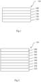
- FIG. 1 is a schematic sectional view of an organic electronic device 100, according to an exemplary embodiment of the present invention.
- the organic electronic device 100 includes a substrate 110, an anode layer 120 and a hole injection layer (HIL) (130).
- the HIL 130 is disposed on the anode layer 120.
- an emission layer (EML) 150, and a cathode layer 190 are disposed.
- the hole injection layer (HIL) 130 may comprise a first and a second sub-layer wherein the first sub-layer is disposed on the anode and the second sub-layer is disposed on the first sub-layer.
- the photoactive layer (PAL) 170 is disposed on the second-sub-layer.
- FIG. 2 is a schematic sectional view of an organic light-emitting diode (OLED) 100, according to an exemplary embodiment of the present invention.
- the OLED 100 includes a substrate 110, an anode layer 120 and a hole injection layer (HIL) 130, The HIL 130 is disposed on the anode layer 120.
- HIL hole injection layer
- EML emission layer
- ETL electron transport layer
- EIL electron injection layer
- cathode layer 190 disposed.
- ETL electron transport layer stack
- ETL electron transport layer stack
- the hole injection layer (HIL) 130 may comprise a first and a second sub-layer wherein the first sub-layer is disposed on the anode and the second sub-layer is disposed on the first sub-layer.
- the hole transport layer (HTL) 140 is disposed on the second-sub-layer.
- Fig. 3 is a schematic sectional view of an OLED 100, according to another exemplary embodiment of the present invention.
- Fig. 2 differs from Fig. 1 in that the OLED 100 of Fig. 2 comprises an electron blocking layer (EBL) 145 and a hole blocking layer (HBL) 155.
- EBL electron blocking layer
- HBL hole blocking layer
- the OLED 100 includes a substrate 110, an anode layer 120, a hole injection layer (HIL) 130, a hole transport layer (HTL) 140, an electron blocking layer (EBL) 145, an emission layer (EML) 150, a hole blocking layer (HBL) 155, an electron transport layer (ETL) 160, an electron injection layer (EIL) 180 and a cathode layer 190.
- HIL hole injection layer
- HTL hole transport layer
- EBL electron blocking layer
- EML emission layer
- HBL hole blocking layer
- ETL electron transport layer
- EIL electron injection layer
- a sealing layer may further be formed on the cathode layer 190, in order to seal the organic electronic device 100.
- various other modifications may be applied thereto.
- the invention is furthermore illustrated by the following examples which are illustrative only and non-binding.
- Organic matrix compound of formula (I), metal complexes of formula (II) and emitter matrix compound of formula (I) may be prepared as described in the literature.
- the rate onset temperature (T RO ) is determined by loading 100 mg organic matrix compound into a VTE source.
- VTE source a point source for organic materials may be used as supplied by Kurt J. Lesker Company (www.lesker.com) or CreaPhys GmbH (http://www.creaphys.com).
- the VTE source is heated at a constant rate of 15 K/min at a pressure of less than 10 -5 mbar and the temperature inside the source measured with a thermocouple.
- Evaporation of the organic matrix compound is detected with a QCM detector which detects deposition of the organic matrix compound on the quartz crystal of the detector. The deposition rate on the quartz crystal is measured in ⁇ ngstrom per second.
- the deposition rate is plotted against the VTE source temperature.
- the rate onset is the temperature at which noticeable deposition on the QCM detector occurs.
- the VTE source is heated and cooled three time and only results from the second and third run are used to determine the rate onset temperature.
- the rate onset temperature may be in the range of ⁇ 110 °C to ⁇ 300 °C, preferably ⁇ 115 °C to ⁇ 290 °C. If the rate onset temperature is too low the evaporation may be too rapid and therefore difficult to control. If the rate onset temperature is too high the evaporation rate may be too low which may result in low tact time and/or decomposition of the metal complex of formula (II) in VTE source may occur due to prolonged exposure to elevated temperatures.
- the rate onset temperature may be in the range of 120 to 300 °C. If the rate onset temperature is too low the evaporation may be too rapid and therefore difficult to control. If the rate onset temperature is too high the evaporation rate may be too low which may result in low tact time.
- the rate onset temperature is an indirect measure of the volatility of a compound. The higher the rate onset temperature the lower is the volatility of a compound.
- the HOMO level and LUMO level are calculated with the program package TURBOMOLE V6.5 (TURBOMOLE GmbH, Litzenhardtstrasse 19, 76135 Düsseldorf, Germany).
- the optimized geometries and the HOMO level and LUMO levels of the molecular structures are determined by applying the hybrid functional B3LYP with a 6-31G* basis set in the gas phase. If more than one conformation is viable, the conformation with the lowest total energy may be selected.
- the HOMO and LUMO levels are recorded in electron volt (eV).
- a l5f2 /cm 2 glass substrate with 90 nm ITO (available from Corning Co.) was cut to a size of 50 mm x 50 mm x 0.7 mm, ultrasonically washed with isopropyl alcohol for 5 minutes and then with pure water for 5 minutes, and washed again with UV ozone for 30 minutes, to prepare the anode layer.
- HIL hole injection layer
- the organic matrix compound was vacuum deposited on the HIL, to form a HTL having a thickness of 128 nm.
- the organic matrix compound in the HTL is selected the same as the organic matrix compound in the HIL.
- the organic matrix compound can be seen in Table 4 and 5.
- N,N-bis(4-(dibenzo[b,d]furan-4-yl)phenyl)-[1,1':4',1"-terphenyl]-4-amine (CAS 1198399-61-9) was vacuum deposited on the HTL, to form an electron blocking layer (EBL) having a thickness of 5 nm.
- EBL electron blocking layer
- a hole blocking layer was formed with a thickness of 5 nm by depositing 2-(3'-(9,9-dimethyl-9H-fluoren-2-yl)-[1,1'-biphenyl]-3-yl)-4,6-diphenyl-1,3,5-triazine on the emission layer EML.
- the electron transporting layer having a thickness of 31 nm was formed on the hole blocking layer by depositing 50 wt.-% 4'-(4-(4-(4,6-diphenyl-1,3,5-triazin-2-yl)phenyl)naphthalen-1-yl)-[1,1'-biphenyl]-4-carbonitrile and 50 wt.-% of LiQ
- Al was evaporated at a rate of 0.01 to 1 ⁇ /s at 10 -7 mbar to form a cathode layer with a thickness of 100 nm on the electron transporting layer.
- the OLED stack was protected from ambient conditions by encapsulation of the device with a glass slide. Thereby, a cavity is formed which may include a getter material for further protection.
- HIL hole injection layer
- the organic matrix compound was vacuum deposited on the HIL, to form a HTL having a thickness of 165 nm.
- the organic matrix compound in the HTL is selected the same as the organic matrix compound in the HIL.
- the organic matrix compound can be seen in Table 6.
- GH-1 comprises EMC-4 and GET-1 in a molar ratio of 1:1.
- the formulas of GET-1 and GD-1 are shown below:
- a hole blocking layer was formed with a thickness of 25 nm by depositing 2,4-diphenyl-6-(3'-(triphenylen-2-yl)-[1,1'-biphenyl]-3-yl)-1,3,5-triazine on the emission layer EML.
- the electron transporting layer having a thickness of 10 nm was formed on the hole blocking layer by depositing 99 vol.-% 3-Phenyl-3H-benzo[b]dinaphtho[2,1-d:1',2'-f]phosphepine-3-oxide and 1 vol.-% Yb.
- Al was evaporated at a rate of 0.01 to 1 ⁇ /s at 10 -7 mbar to form a cathode layer with a thickness of 100 nm on the electron transporting layer.
- the OLED stack is protected from ambient conditions by encapsulation of the device with a glass slide. Thereby, a cavity is formed which may include a getter material for further protection.
- the hole injection layer comprising a first and a second sub-layer was vacuum deposited on the anode layer.
- a metal complex was vacuum deposited on the anode layer to form a first sub-layer with a thickness of 3 or 5 nm, see Table 7.
- HAT-CN was vacuum deposited on the anode layer to form a first sub-layer with a thickness of 3 or 5 nm, see Table 7.
- the organic matrix compound was vacuum deposited on the first sub-layer to form a second sub-layer with a thickness of 7 or 5 nm, see Table 7.
- an organic matrix compound was vacuum deposited on the hole injection layer to form a HTL.
- the organic matrix compound in the HTL is selected the same as the organic matrix compound in the HIL, see Table 7.
- the thickness is selected in such a way, that the thickness of the second sub-layer and the thickness of the HTL add up to 128 nm in total.
- N,N-bis(4-(dibenzo[b,d]furan-4-yl)phenyl)-[1,1':4',1"-terphenyl]-4-amine (CAS 1198399-61-9) was vacuum deposited on the HTL, to form an electron blocking layer (EBL) having a thickness of 5 nm.
- EBL electron blocking layer
- a hole blocking layer was formed with a thickness of 5 nm by depositing 2-(3'-(9,9-dimethyl-9H-fluoren-2-yl)-[1,1'-biphenyl]-3-yl)-4,6-diphenyl-1,3,5-triazine on the emission layer EML.
- the electron transporting layer having a thickness of 31 nm was formed on the hole blocking layer by depositing 50 wt.-% 4'-(4-(4-(4,6-diphenyl-1,3,5-triazin-2-yl)phenyl)naphthalen-1-yl)-[1,1'-biphenyl]-4-carbonitrile and 50 wt.-% of LiQ
- Al was evaporated at a rate of 0.01 to 1 ⁇ /s at 10 -7 mbar to form a cathode layer with a thickness of 100 nm on the electron transporting layer.
- the OLED stack was protected from ambient conditions by encapsulation of the device with a glass slide. Thereby, a cavity is formed which may include a getter material for further protection.
- the current efficiency is measured at 20°C.
- the current-voltage characteristic is determined using a Keithley 2635 source measure unit, by sourcing an operating voltage U in V and measuring the current in mA flowing through the device under test.
- the voltage applied to the device is varied in steps of 0.1V in the range between 0V and 10V. To protect the instruments from damage, the measurement was stopped at 10 V.
- Table 1 Chemical formulas and physical properties of organic matrix compounds Name Chemical formula HOMO level (eV) T RO (°C) 9-phenyl-10-(3',4',5'-triphenyl-[1,1':2',1"-terphenyl]-3-yl)anthracene - 5.04 210 OMC-1 1,3-bis(10-phenylanthracen-9-yl)benzene -5.08 230 OMC-2 9-phenyl-10-(3'-(9-phenyl-9H-fluoren-9-yl)-[1,1'-biphenyl]-3-yl)anthracene - 5.08 226 OMC-3 9-([1,1'-biphenyl]-3-yl)
- OMC-10 2,7-di([1,1'-biphenyl]-4-yl)spiro[fluorene-9,9'-xanthene] - 5.38
- OMC-11 7-(3-(9H-carbazol-9-yl)phenyl)dibenzo[c,h]acridi ne - 5.42
- OMC-12 4,4',4"-(1,3,5-Benzenetriyl)tris[dibenzothi ophene] -5.67 272 OMC-13
- the organic matrix compounds have rate onset temperatures suitable for mass production of organic electronic devices.
- Table 2 Metal complexes of formula (II) Name Chemical formula T RO (°C) MC-1 Li TFSI 222 MC-2 K TFSI 236 MC-3 Cs TFSI 224 MC-4 Ag TFSI 258 MC-5 Mg (TFSI) 2 243 MC-6 Mn (TFSI) 2 229 MC-7 Sc (TFSI) 3 258 MC-8 Mg [N(SO 2 i C 3 F 7 ) 2 ] 2 166 MC-9 Zn [N(SO 2 i C 3 F 7 ) 2 ] 2 118 MC-10 Ag [N(SO 2 i C 3 F 7 ) 2 ] 232 MC-11 Ag [N(SO 2 C 3 F 7 ) 2 ] 254 MC-12 Ag [N(SO 2 C 4 F 9 ) 2 262 MC-13 Ag [N(SO 2 CF 3 )(SO 2 C 4 F 9 )] 230 MC
- the metal complexes of formula (II) have rate onset temperatures suitable for mass production of organic electronic devices.
- Table 3 Chemical formulas and physical properties of emitter matrix compounds Name Chemical formula HOMO level (eV) T RO (°C) 9-phenyl-10-(3',4',5'-triphenyl-[1,1':2',1"-terphenyl]-3-yl)anthracene - 5.04 210 EMC-1 1,3-bis(10-phenylanthracen-9-yl)benzene -5.08 230 EMC-2 9-phenyl-10-(3'-(9-phenyl-9H-fluoren-9-yl)-[1,1'-biphenyl]-3-yl)anthracene - 5.08 226 EMC-3 9-([1,1'-biphenyl]-3-y
- the emitter matrix compounds have rate onset temperatures suitable for mass production of organic electronic devices.
- OLEDs comprising a hole injection layer comprising 70 vol.-% organic matrix compound OMC-10 and 30 vol.-% metal complex of formula (II) and an emission layer comprising 97 vol.-% emitter matrix compound EMC-6 and 3 vol.-% fluorescent blue emitter dopant.
- OMC-10 has a HOMO level of -5.30 eV.
- the emitter matrix compound EMC-6 has a HOMO level of -5.13 eV.
- HAT-CN a state of the art material, is used at a concentration of 30 vol.-%.
- HAT-CN has the formula shown below:
- HAT-CN has a HOMO of -8.83 eV.
- the operating voltage is over 10 V.
- the hole injection layer comprises Cu(TFSI) 2 as metal complex.
- the operating voltage is substantially improved to 6.9 V.
- the hole injection layer comprises a different Cu(II) complex, namely MC-24.
- the TFSI ligand has been replaced by an amide ligand comprising one trifluoro methyl and one substituted aryl group.
- the operating voltage is further improved to 6.3 V.
- the hole injection layer comprises MC-6.
- the Cu(II) cation has been replaced by a Mn(II) cation.
- the operating voltage compared to example 1 is improved from 6.9 to 5.3 V.
- the hole injection layer comprises a Mg complex.
- Cu(II) cation has been replaced by Mg(II) cation.
- the operating voltage is improved from 6.3 to 5.4 V.
- the hole injection layer comprises a Zn(II) complex.
- the Mg(II) cation has been replaced by a Zn(II) cation and the amide ligand has been replaced by a ligand comprising an N-aryl group.
- the operating voltage is still within the range acceptable for mass production.
- Table 5 are shown operating voltages at 10 mA/cm 2 in OLEDs comprising a fluorescent blue emitter and a hole injection layer comprising 70 vol.-% organic matrix compound and 30 vol.-% metal complex of formula (II) and an emission layer comprising 97 vol.-% emitter matrix compound EMC-6 and 3 vol.-% fluorescent blue emitter.
- the emitter matrix compound EMC-6 has a HOMO level of -5.13 eV.
- Table 5 Performance of OLEDs comprising a fluorescent blue emitter and emitter matrix compound EMC-6 Organic matrix compound (OMC) HOMO level (OMC) [eV] HOMO level (EMC) - HOMO level (OMC) [eV] Metal complex U at 10 mA/cm 2 [V] Comparative example 2 OMC-5 -5.10 -0.03 HAT-CN > 10 Comparative example 3 OMC-13 -5.67 0.54 HAT-CN > 10 Example 6 OMC-5 -5.10 -0.03 MC-29 4.1 Example 7 OMC-6 -5.13 0 MC-29 4.1 Example 8 OMC-7 -5.13 0 MC-29 5.1 Example 9 OMC-9 -5.28 0.15 MC-29 5.7
- Example 10 OMC-10 -5.30 0.17 MC-29 5.9
- Example 11 OMC-13 -5.67 0.54 MC-29 7.0
- the hole injection layer comprises organic matrix compound OMC-5 and 30 vol.-% HAT-CN.
- HAT-CN is free of metal complex.
- OMC-5 comprises an anthracene group.
- the HOMO level of OMC-5 is -5.10 eV.
- the offset in HOMO level between the emitter matrix compound and the organic matrix compound is -0.03 eV.
- the operating voltage is over 10 V.
- the hole injection layer comprises organic matrix compound OMC-13 and 30 vol.-% HAT-CN.
- OMC-13 comprises three dibenzofuranyl groups.
- the HOMO level is -5.67 eV.
- the offset in HOMO level between the emitter matrix compound and the organic matrix compound is 0.54 eV.
- the operating voltage is over 10 V.
- the hole injection layer comprises OMC-5 and metal complex MC-29.
- the operating voltage is reduced substantially to 4.1 V.
- the hole injection layer comprises OMC-6 and MC-29.
- OMC-6 comprises an anthracene and a dibenzofuranyl group.
- the same compound is used in the hole injection layer and in the emission layer.
- the offset in HOMO level between the emitter matrix compound and the organic matrix compound is 0 eV.
- the operating voltage is unchanged at 4.1 V.
- the hole injection layer comprises OMC-7 and MC-29.
- OMC-7 comprises an anthracene and a dibenzofuranyl group.
- the HOMO level is -5.13 eV.
- the offset in HOMO level between the emitter matrix compound and the organic matrix compound is 0 eV.
- the operating voltage is a little bit higher than in example 7. However, the operating voltage is substantially reduced compared to comparative examples 2 and 3.
- the hole injection layer comprises OMC-9 and MC-29.
- OMC-9 comprises a dibenzoacridine and a carbazole group.
- the HOMO level is -5.28 eV.
- the offset in HOMO level between the emitter matrix compound and the organic matrix compound is increased to 0.15 eV.
- the operating voltage is a little bit higher than in example 8. However, the operating voltage is substantially reduced compared to comparative examples 2 and 3.
- the hole injection layer comprises OMC-10 and MC-29.
- OMC-10 comprises a two carbazole groups.
- the HOMO level is -5.30 eV.
- the offset in HOMO level between the emitter matrix compound and the organic matrix compound is increased to 0.17 eV.
- the operating voltage is still substantially reduced compared to comparative examples 2 and 3.
- the hole injection layer comprises OMC-13 and MC-29.
- OMC-13 comprises three dibenzofuranyl groups.
- the HOMO level is -5.67 eV.
- the offset in HOMO level between the emitter matrix compound and the organic matrix compound is increased further to 0.54 eV.
- the operating voltage is a little bit higher than in example 10. However, the operating voltage is substantially reduced compared to comparative examples 2 and 3.
- Table 6 are shown operating voltages at 10 mA/cm 2 in OLEDs comprising a phosphorescent green emitter and a hole injection layer comprising an organic matrix compound and 30 vol.-% metal complex of formula (II) and an emission layer comprising 70 vol.-% of a composition comprising EMC-4 and GET-1 in a molar ratio of 1:1 and 30 vol.-% of phosphorescent green emitter GD-1. If the emission layer comprises a composition of two or more emitter matrix compounds, the emitter matrix compound with the HOMO level closer to vacuum level is considered.
- the emitter matrix compound EMC-4 has a HOMO level of -5.09 eV.
- GET-1 has a HOMO level of -5.69 eV.
- Table 6 Performance of OLEDs comprising a phosphorescent green emitter Organic matrix compound (OMC) HOMO level (OMC) [eV] HOMO level (EMC) - HOMO level (OMC) [eV] Metal complex U at 10 mA/cm 2 [V]
- Comparative example 4 OMC-5 -5.10 0.01 HAT-CN > 10
- Example 12 OMC-5 -5.10 0.01 MC-29 4.5
- Comparative example 5 OMC-10 -5.30 0.21 HAT-CN > 10
- Example 13 OMC-10 -5.30 0.21 MC-29 6.3
- the hole injection layer comprises organic matrix compound OMC-5 and 30 vol.-% HAT-CN.
- HAT-CN is free of metal complex.
- OMC-5 comprises an anthracene group.
- the HOMO level of OMC-5 is -5.10 eV.
- the offset in HOMO level between the emitter matrix compound and the organic matrix compound is 0.01 eV.
- the operating voltage is over 10 V.
- the hole injection layer comprises OMC-5 and metal complex MC-29.
- the operating voltage is reduced substantially to 4.1 V.
- the hole injection layer comprises organic matrix compound OMC-10 and 30 vol.-% HAT-CN.
- OMC-10 comprises two carbazole groups.
- the HOMO level of OMC-10 is -5.30 eV.
- the offset in HOMO level between the emitter matrix compound and the organic matrix compound is 0.21 eV.
- the operating voltage is over 10 V.
- the hole injection layer comprises OMC-10 and metal complex MC-29.
- the operating voltage is reduced substantially to 6.3 V.
- Table 7 are shown operating voltages at 10 mA/cm 2 in OLEDs comprising a fluorescent blue emitter and a hole injection layer, wherein the hole injection layer comprises a first sub-layer consisting of metal complex of formula (II) and a second sub-layer consisting of organic matrix compound.
- the emission layer comprises 97 vol.-% emitter matrix compound EMC-6 and 3 vol.-% fluorescent blue emitter.
- the first sub-layer comprises HAT-CN as a state-of-the-art hole injection material with a thickness of 3 nm.
- HAT-CN is free of metal complex.
- the second sub-layer comprises organic matrix compound OMC-6.
- the offset in HOMO level between the emitter matrix compound and the organic matrix compound is -0.03 eV.
- the operating voltage is over 10 V.
- the first sub-layer comprises HAT-CN and the second sub-layer comprises organic matrix compound OMC-7.
- the offset in HOMO level between the emitter matrix compound and the organic matrix compound is 0.15 eV.
- the operating voltage is over 10 V.
- the first sub-layer comprises HAT-CN and the second sub-layer comprises organic matrix compound OMC-10.
- the offset in HOMO level between the emitter matrix compound and the organic matrix compound is 0.17 eV.
- the operating voltage is over 10 V.
- the first sub-layer comprises metal complex MC-29 with a thickness of 3 nm.
- the second sub-layer comprises organic matrix compound OMC-6.
- the offset in HOMO level between the emitter matrix compound and the organic matrix compound is - 0.03 eV.
- the operating voltage is 4.0 V and thereby substantially improved over comparative example 6.
- the first sub-layer is the same as in Example 14.
- the second sub-layer comprises a range of organic matrix compounds with a HOMO level further away from vacuum level than OMC-6.
- the offset in HOMO level between the emitter matrix compound and the organic matrix compounds is in the range of 0 to 0.17 eV.
- the operating voltage is substantially improved over comparative examples 6, 7 and 8.
- the first sub-layer comprises metal complex MC-27.
- MC-27 differs from MC-29 in the metal cation and ligand, see Table 2.
- the second sub-layer comprises a range of organic matrix compounds.
- the offset in HOMO level between the emitter matrix compound and the organic matrix compound is in the range of -0.03 to 0.15 eV. In all examples, the operating voltage is substantially improved over comparative examples 6, 7 and 8.
- the first sub-layer comprises metal complex MC-30.
- MC-30 differs from MC-29 in the metal cation and ligand, see Table 2.
- the second sub-layer comprises OMC-7.
- the offset in HOMO level between the emitter matrix compound and the organic matrix compound is 0.15 eV.
- the operating voltage is 6.6 V and thereby improved over comparative example 7.
- the first sub-layer comprises HAT-CN as a state-of-the-art hole injection material with a thickness of 5 nm.
- the second sub-layer comprises a range of organic matrix compounds.
- the offset in HOMO level between the emitter matrix compound and the organic matrix compound is in the range of -0.03 to 0.17 eV.
- the operating voltage is over 10 V.
- the first sub-layer comprises metal complex MC-29 with a thickness of 5 nm.
- the second sub-layer comprises organic matrix compound OMC-6.
- the offset in HOMO level between the emitter matrix compound and the organic matrix compound is -0.03 eV.
- the operating voltage is 4.0 V and thereby substantially improved over comparative example 9.
- the performance is comparable to Example 14.
- the first sub-layer is the same as in Example 22.
- the second sub-layer comprises various organic matrix compounds with a HOMO level further away from vacuum level than OMC-6.
- the offset in HOMO level between the emitter matrix compound and the organic matrix compound is in the range of 0 to 0.17 eV. In all examples, the operating voltage is substantially improved over comparative examples 9, 10 and 11.
- the first sub-layer comprises metal complex MC-27.
- MC-27 differs from MC-29 in the metal cation and ligand, see Table 2.
- the second sub-layer comprises various organic matrix compounds.
- the offset in HOMO level between the emitter matrix compound and the organic matrix compound is in the range of 0 to 0.15 eV. In all examples, the operating voltage is substantially improved over comparative examples 9, 10 and 11.
- the first sub-layer comprises metal complex MC-30.
- MC-30 differs from MC-29 in the metal cation and ligand, see Table 2.
- the second sub-layer comprises OMC-7.
- the offset in HOMO level between the emitter matrix compound and the organic matrix compound is 0.15 eV.
- the operating voltage is 5.4 V and thereby improved over comparative example 10.
- HIL hole injection layer
- the hole injection layer comprises a first and a second sub-layer Composition of first sub-layer Thickness of first sub-layer [nm]
- Comparativ e example 6 HAT-CN 3 OMC-6 -5.10 7 OMC-6 -0.03 > 10
Landscapes
- Chemical & Material Sciences (AREA)
- Engineering & Computer Science (AREA)
- Materials Engineering (AREA)
- Physics & Mathematics (AREA)
- Inorganic Chemistry (AREA)
- Spectroscopy & Molecular Physics (AREA)
- Optics & Photonics (AREA)
- Crystallography & Structural Chemistry (AREA)
- Electroluminescent Light Sources (AREA)
Claims (15)
- Dispositif électronique organique comprenant une couche d'anode (120), une couche de cathode (190), au moins une couche d'émission (EML) (150) et au moins une couche d'injection de trous (HIL) (130), la couche d'injection de trous étant agencée entre la couche d'anode et l'au moins une couche d'émission ;- la couche d'injection de trous comprenant un composé de matrice organique (OMC) et un complexe métallique, le complexe métallique ayant la formule (II) :
Mn⊕(L⊖)n (II),
M étant un ion métallique,n étant la valence de M, n étant un entier de 1 à 4L étant un ligand ; et- l'au moins une couche d'émission comprenant au moins un composé de matrice émetteur (EMC), le niveau HOMO du composé de matrice émetteur (EMC) et le niveau HOMO du composé de matrice organique (OMC) satisfaisant l'équation suivante :-0,24 eV < [niveau HOMO (EMC) - niveau HOMO (OMC)] ≤ 0,8 eV ; le composé de matrice organique (OMC) et le composé de matrice émetteur (EMC) ayant la formule (I) :
(Ar1)k-(Ar2)m-Ar3-(Ar4)p-(Ar5)q-(Ar6)r (I),
k, m, q, r étant indépendamment les uns des autres 0, 1 ou 2,p étant 1, 2 ou 3, Ar1 à Ar6 étant indépendamment choisis parmi un cycle insaturé substitué ou non substitué à 5 à 7 chaînons d'un hétérocycle, un C6 à C30 aryle substitué ou non substitué ou un C3 à C30 hétéroaryle substitué ou non substitué, un fluorène substitué ou non substitué, ou un système cyclique condensé comprenant 2 à 6 cycles substitués ou non substitués à 5 à 7 chaînons et les cycles étant choisis dans le groupe comprenant (i) un cycle insaturé à 5 à 7 chaînons d'un hétérocycle, (ii) un cycle insaturé à 5 à 6 chaînons d'un hétérocycle aromatique, (iii) un cycle insaturé à 5 à 7 chaînons d'un non-hétérocycle, (iv) un cycle à 6 chaînons d'un non-hétérocycle aromatique ;les substituants étant choisis dans le groupe H, D, C1 à C12 alkyle, C6 à C18 aryle non substitué, C3 à C18 hétéroaryle non substitué, un système cyclique condensé comprenant 2 à 6 cycles non substitués à 5 à 7 chaînons et les cycles étant choisis dans le groupe comprenant un cycle insaturé à 5 à 7 chaînons d'un hétérocycle, un cycle insaturé à 5 à 6 chaînons d'un hétérocycle aromatique, un cycle insaturé à 5 à 7 chaînons d'un non-hétérocycle, et un cycle à 6 chaînons d'un non-hétérocycle aromatique ;et le composé de matrice organique (OMC) et le composé de matrice émetteur (EMC) étant choisis les mêmes ou choisis différents, et les niveaux HOMO étant calculés avec le package de programme TURBOMOLE V6.5, les géométries optimisées et les niveaux HOMO des structures moléculaires étant déterminés en appliquant du B3LYP fonctionnel hybride avec un ensemble de base 6-31G* dans la phase gazeuse.
 - Dispositif électronique organique selon la revendication 1, la couche d'injection de trous étant non émissive.
- Dispositif électronique organique selon la revendication 1 ou 2, la couche d'injection de trous étant agencée adjacente à la couche d'anode, en variante en contact direct avec la couche d'anode.
- Dispositif électronique organique selon l'une quelconque des revendications précédentes 1 à 3, le niveau HOMO du composé de matrice organique (OMC) étant plus à l'écart du niveau de vide que le niveau HOMO de la N4,N4‴-di(naphtalén-1-yl)-N4,N4‴-diphényl-[1,1':4',1":4",1‴-quaterphényl]-4,4‴-diamine lorsqu'il est déterminé dans les mêmes conditions.
- Dispositif électronique organique selon l'une quelconque des revendications précédentes 1 à 4, le composé de matrice organique (OMC) satisfaisant l'équation suivante :

- Dispositif électronique organique selon l'une quelconque des revendications précédentes 1 à 5, le composé de matrice organique (OMC) et le composé de matrice émetteur (EMC) ayant la formule (I) :
(Ar1)k-(Ar2)m-Ar3-(Ar4)p-(Ar5)q-(Ar6)r (I),
k, m, q, r étant indépendamment les uns des autres 0, 1 ou 2,p étant 1, 2 ou 3,2 ≤ k + m + q + r + p ≤ 11,Ar1 à Ar6 étant indépendamment choisis parmi biphénylène substitué ou non substitué, fluorène substitué ou non substitué, naphtalène substitué ou non substitué, anthracène substitué ou non substitué, phénanthrène substitué ou non substitué, pyrène substitué ou non substitué, pérylène substitué ou non substitué, triphénylène substitué ou non substitué, tétracène substitué ou non substitué, tétraphène substitué ou non substitué, dibenzofurane substitué ou non substitué, dibenzothiophène substitué ou non substitué, xanthène substitué ou non substitué, carbazole substitué ou non substitué, azépine substituée ou non substituée, dibenzo[b,f]azépine substituée ou non substituée, 9,9'-spirobi[fluorène], spiro[fluorène-9,9'-xanthène] substitué ou non substitué, 9,14-dihydrodibenzo[2,3:6,7]azépino[4,5-b]indole substitué ou non substitué, ou un système cyclique condensé aromatique substitué ou non substitué comprenant au moins trois cycles aromatiques substitués ou non substitués choisis dans le groupe comprenant des cycles à 5 chaînons non hétéro substitués ou non substitués, hétéro substitués ou non substitués, des cycles substitués ou non substitués à 6 chaînons et/ou des cycles substitués ou non substitués à 7 chaînons, fluorène substitué ou non substitué, ou un système cyclique condensé comprenant 2 à 6 cycles substitués ou non substitués à 5 à 7 chaînons et les cycles étant choisis dans le groupe comprenant (i) un cycle insaturé à 5 à 7 chaînons d'un hétérocycle, (ii) un cycle insaturé à 5 à 6 chaînons d'un hétérocycle aromatique, (iii) un cycle insaturé à 5 à 7 chaînons d'un non hétérocycle, (iv) un cycle à 6 chaînons d'un non hétérocycle aromatique,les substituants étant choisis dans le groupe H, D, C1 à C12 alkyle, C6 à C18 aryle non substitué, C3 à C18 hétéroaryle non substitué, un système cyclique condensé comprenant 2 à 6 cycles non substitués à 5 à 7 chaînons et les cycles étant choisis dans le groupe comprenant un cycle insaturé à 5 à 7 chaînons d'un hétérocycle, un cycle insaturé à 5 à 6 chaînons d'un hétérocycle aromatique, un cycle insaturé à 5 à 7 chaînons d'un non-hétérocycle, et un cycle à 6 chaînons d'un non-hétérocycle aromatique ;et le composé de matrice organique (OMC) et le composé de matrice émetteur (EMC) étant choisis les mêmes ou choisis différents, préférablement différents. - Dispositif électronique organique selon l'une quelconque des revendications précédentes 1 à 6, le composé de matrice organique (OMC) de la couche d'injection de trous et/ou le composé de matrice émetteur (EMC) ayant un poids moléculaire Mw de ≥ 400 et ≤ 2 000 g/mole, préférablement un poids moléculaire Mw de ≥ 450 et ≤ 1 500 g/mole, de manière en outre préférée un poids moléculaire Mw de ≥ 500 et ≤ 1 000 g/mole, de plus de manière préférée un poids moléculaire Mw de ≥ 550 et ≤ 900 g/mole, également de manière préférée un poids moléculaire Mw de ≥ 600 et ≤ 800 g/mole.
- Dispositif électronique organique selon l'une quelconque des revendications précédentes 1 à 7, M étant choisi parmi un ion métallique, le métal correspondant ayant une valeur d'électronégativité selon Allen inférieure à 2,4, préférablement M étant choisi parmi un métal alcalin, alcalino-terreux, des terres rares ou de transition, de manière en outre préférée M étant choisi parmi un métal doté d'une masse atomique ≥ 24 Da, de plus de manière préférée M étant choisi parmi un métal doté d'une masse atomique ≥ 24 Da et M ayant un nombre d'oxydation ≥ 2.
- Dispositif électronique organique selon l'une quelconque des revendications précédentes 1 à 8, le complexe métallique ayant un poids moléculaire Mw de ≥ 287 et ≤ 2 000 g/mole, préférablement un poids moléculaire Mw de ≥ 400 et ≤ 1 500 g/mole, de manière en outre préférée un poids moléculaire Mw de ≥ 580 et ≤ 1 500 g/mole, de plus de manière préférée un poids moléculaire Mw de ≥ 580 et ≤ 1 400 g/mole.
- Dispositif électronique organique selon l'une quelconque des revendications précédentes 1 à 9, L étant choisi dans un groupe comprenant- au moins trois atomes de carbone, en variante au moins quatre atomes de carbone, et/ou- au moins deux atomes d'oxygène ou un atome d'oxygène et un atome d'azote, deux à quatre atomes d'oxygène, deux à quatre atomes d'oxygène et zéro à deux atomes d'azote, et/ou- au moins un ou plusieurs groupes choisis parmi halogène, F, CN, C1 à C6 alkyle substitué ou non substitué, C1 à C6 alcoxy substitué ou non substitué, en variante deux ou plus groupes choisis parmi halogène, F, CN, C1 à C6 alkyle substitué ou non substitué, C1 à C6 alcoxy substitué ou non substitué, au moins un ou plusieurs groupes choisis parmi halogène, F, CN, C1 à C6 alkyle substitué, C1 à C6 alcoxy substitué, en variante deux ou plus groupes choisis parmi halogène, F, CN, C1 à C6 alkyle perfluoré, C1 à C6 alcoxy perfluoré, un ou plusieurs groupes choisis parmi C1 à C6 alkyle substitué ou non substitué, C6 à C12 aryle substitué ou non substitué, et/ou C3 à C12 hétéroaryle substitué ou non substitué,les substituants étant choisis parmi D, C6 aryle, C3 à C9 hétéroaryle, C1 à C6 alkyle, C1 à C6 alcoxy, C3 à C6 alkyle ramifié, C3 à C6 alkyle cyclique, C3 à C6 alcoxy ramifié, C3 à C6 alcoxy cyclique, C1 à C16 alkyle partiellement ou perfluoré, C1 à C16 alcoxy partiellement ou perfluoré, C1 à C6 alkyle partiellement ou perdeutéré, C1 à C6 alcoxy partiellement ou perdeutéré, COR6, COOR6, halogène, F ou CN ;R6 étant choisi parmi C6 aryle, C3 à C9 hétéroaryle, C1 à C6 alkyle, C1 à C6 alcoxy, C3 à C6 alkyle ramifié, C3 à C6 alkyle cyclique, C3 à C6 alcoxy ramifié, C3 à C6 alcoxy cyclique, C1 à C16 alkyle partiellement ou perfluoré, C1 à C16 alcoxy partiellement ou perfluoré, C1 à C6 alkyle partiellement ou perdeutéré, C1 à C6 alcoxy partiellement ou perdeutéré.
- Dispositif électronique organique selon l'une quelconque des revendications précédentes 1 à 10, le composé de matrice organique (OMC) et le composé de matrice émetteur (EMC) étant exempts d'hétéroatomes qui ne font pas partie d'un cycle aromatique et/ou partie d'un cycle insaturé à 7 chaînons, préférablement le composé selon la formule (I) étant exempt d'atomes de N à l'exception d'atomes de N qui font partie d'un cycle aromatique ou font partie d'un cycle insaturé à 7 chaînons.
- Dispositif électronique organique selon l'une quelconque des revendications précédentes 1 à 11, n étant un entier de 1 à 4, préférablement 1 à 3, également de manière préférée 2 ou 3.
- Dispositif électronique organique selon l'une quelconque des revendications précédentes 1 à 12, le complexe métallique étant choisi parmi les formules suivantes (IIa) à (IIe) et préférablement (IIa) à (IId)


 M étant un ion métallique ;n étant la valence de M, n étant un entier de 1 à 4 ;A1 et A2 étant indépendamment choisis parmi C1 à C12 alkyle substitué ou non substitué, C6 à C12 aryle substitué ou non substitué, C3 à C12 hétéroaryle substitué ou non substitué ;A3 étant choisi parmi H, D, C1 à C12 alkyle substitué ou non substitué, C6 à C12 aryle substitué ou non substitué, C3 à C12 hétéroaryle substitué ou non substitué ;les substituants de A1, A2 et/ou A3 étant indépendamment choisis parmi D, C6 aryle, C3 à C9 hétéroaryle, C1 à C6 alkyle, C1 à C6 alcoxy, C3 à C6 alkyle ramifié, C3 à C6 alkyle cyclique, C3 à C6 alcoxy ramifié, C3 à C6 alcoxy cyclique, C1 à C16 alkyle partiellement ou perfluoré, C1 à C16 alcoxy partiellement ou perfluoré, C1 à C6 alkyle partiellement ou perdeutéré, C1 à C6 alcoxy partiellement ou perdeutéré, COR1, COOR1, halogène, F ou CN,R1 étant choisi parmi C6 aryle, C3 à C9 hétéroaryle, C1 à C6 alkyle, C1 à C6 alcoxy, C3 à C6 alkyle ramifié, C3 à C6 alkyle cyclique, C3 à C6 alcoxy ramifié, C3 à C6 alcoxy cyclique, C1 à C16 alkyle partiellement ou perfluoré, C1 à C16 alcoxy partiellement ou perfluoré, C1 à C6 alkyle partiellement ou perdeutéré, C1 à C6 alcoxy partiellement ou perdeutéré.
 - Dispositif électronique organique selon la revendication 13, au moins l'un parmi A1, A2 et A3 comprenant un substituant, au moins l'un des substituants de A1, A2 et A3 étant indépendamment choisi parmi C3 à C9 hétéroaryle, C1 à C6 alcoxy, C3 à C6 alcoxy ramifié, C3 à C6 alcoxy cyclique, C1 à C16 alkyle partiellement ou perfluoré, C1 à C16 alcoxy partiellement ou perfluoré, C1 à C6 alcoxy partiellement ou perdeutéré, COR1, COOR1, halogène, F ou CN ; préférablement au moins l'un parmi A1, A2 et A3 comprenant au moins deux substituants, les substituants sur A1, A2 et A3 étant indépendamment choisis parmi C3 à C9 hétéroaryle, C1 à C6 alcoxy, C3 à C6 alcoxy ramifié, C3 à C6 alcoxy cyclique, C1 à C16 alkyle partiellement ou perfluoré, C1 à C16 alcoxy partiellement ou perfluoré, C1 à C6 alcoxy partiellement ou perdeutéré, COR1, COOR1, halogène, F ou CN ; et de manière en outre préférée A1, A2 et A3 comprenant au moins un substituant indépendamment choisi parmi halogène, F, CF3, C2F5, C3F7, C4F9, OCF3, OC2F5, ou CN ; et de plus de manière préférée A1, A2 et A3 comprenant au moins deux substituants indépendamment choisis parmi halogène, F, CF3, C2F5, C3F7, C4F9, OCF3, OC2F5 ou CN, R1 étant tel que défini dans la revendication 13.
- Dispositif électronique organique selon l'une quelconque des revendications précédentes 1 à 14, le dispositif électronique organique étant un dispositif émetteur de lumière ou un dispositif d'affichage.
Priority Applications (1)
| Application Number | Priority Date | Filing Date | Title |
|---|---|---|---|
| EP25164040.5A EP4550997A3 (fr) | 2020-01-28 | 2021-01-27 | Dispositif électronique organique comprenant une couche d'anode, une couche de cathode, au moins une couche d'émission (eml) et au moins une couche d'injection de trous (hil) |
Applications Claiming Priority (2)
| Application Number | Priority Date | Filing Date | Title |
|---|---|---|---|
| EP20154092.9A EP3859811B1 (fr) | 2020-01-28 | 2020-01-28 | Dispositif électronique organique comprenant une couche d'anode, une couche de cathode, au moins une couche d'émission (eml) et au moins une couche d'injection par trous (hil) |
| PCT/EP2021/051885 WO2021151959A1 (fr) | 2020-01-28 | 2021-01-27 | Dispositif électronique organique comprenant une couche d'anode, une couche de cathode, au moins une couche d'émission (eml) et au moins une couche d'injection de trous (hil) |
Related Child Applications (1)
| Application Number | Title | Priority Date | Filing Date |
|---|---|---|---|
| EP25164040.5A Division EP4550997A3 (fr) | 2020-01-28 | 2021-01-27 | Dispositif électronique organique comprenant une couche d'anode, une couche de cathode, au moins une couche d'émission (eml) et au moins une couche d'injection de trous (hil) |
Publications (2)
| Publication Number | Publication Date |
|---|---|
| EP4097777A1 EP4097777A1 (fr) | 2022-12-07 |
| EP4097777B1 true EP4097777B1 (fr) | 2025-03-19 |
Family
ID=69374229
Family Applications (3)
| Application Number | Title | Priority Date | Filing Date |
|---|---|---|---|
| EP20154092.9A Active EP3859811B1 (fr) | 2020-01-28 | 2020-01-28 | Dispositif électronique organique comprenant une couche d'anode, une couche de cathode, au moins une couche d'émission (eml) et au moins une couche d'injection par trous (hil) |
| EP21702266.4A Active EP4097777B1 (fr) | 2020-01-28 | 2021-01-27 | Dispositif électronique organique comprenant une couche d'anode, une couche de cathode, au moins une couche d'émission (eml) et au moins une couche d'injection par trous (hil) |
| EP25164040.5A Pending EP4550997A3 (fr) | 2020-01-28 | 2021-01-27 | Dispositif électronique organique comprenant une couche d'anode, une couche de cathode, au moins une couche d'émission (eml) et au moins une couche d'injection de trous (hil) |
Family Applications Before (1)
| Application Number | Title | Priority Date | Filing Date |
|---|---|---|---|
| EP20154092.9A Active EP3859811B1 (fr) | 2020-01-28 | 2020-01-28 | Dispositif électronique organique comprenant une couche d'anode, une couche de cathode, au moins une couche d'émission (eml) et au moins une couche d'injection par trous (hil) |
Family Applications After (1)
| Application Number | Title | Priority Date | Filing Date |
|---|---|---|---|
| EP25164040.5A Pending EP4550997A3 (fr) | 2020-01-28 | 2021-01-27 | Dispositif électronique organique comprenant une couche d'anode, une couche de cathode, au moins une couche d'émission (eml) et au moins une couche d'injection de trous (hil) |
Country Status (5)
| Country | Link |
|---|---|
| EP (3) | EP3859811B1 (fr) |
| JP (1) | JP2023513466A (fr) |
| CN (1) | CN115088090B (fr) |
| TW (1) | TW202146421A (fr) |
| WO (1) | WO2021151959A1 (fr) |
Families Citing this family (3)
| Publication number | Priority date | Publication date | Assignee | Title |
|---|---|---|---|---|
| KR20250073115A (ko) * | 2022-09-19 | 2025-05-27 | 노발레드 게엠베하 | 애노드층, 캐소드층, 제1 발광층, 정공주입층 및 금속을 함유하는 화합물을 포함하는 제1 정공수송층을 포함하는 전기발광 장치 |
| EP4340581A1 (fr) * | 2022-09-19 | 2024-03-20 | Novaled GmbH | Dispositif électroluminescent comprenant une couche d'anode, une couche de cathode, une première couche d'émission, une couche d'injection de trous. |
| WO2024133366A1 (fr) | 2022-12-23 | 2024-06-27 | Merck Patent Gmbh | Dispositif électronique |
Citations (6)
| Publication number | Priority date | Publication date | Assignee | Title |
|---|---|---|---|---|
| WO2016188604A1 (fr) | 2015-05-22 | 2016-12-01 | Merck Patent Gmbh | Composition comprenant un semi-conducteur organique et un complexe métallique |
| WO2018158232A1 (fr) | 2017-03-01 | 2018-09-07 | Merck Patent Gmbh | Dispositif électroluminescent organique |
| US20180331308A1 (en) | 2015-12-15 | 2018-11-15 | Osram Oled Gmbh | Organic Electronic Component and Use of a Fluorinated Sulfonimide Metal Salt |
| EP3425690A1 (fr) | 2017-07-03 | 2019-01-09 | Samsung Electronics Co., Ltd. | Dispositif électroluminescent organique |
| WO2021048044A1 (fr) | 2019-09-11 | 2021-03-18 | Technische Universität Dresden | Complexes de cérium (iv) et leur utilisation dans l'électronique organique |
| EP3133663B1 (fr) | 2015-08-18 | 2022-06-15 | Novaled GmbH | Amides métalliques destinés à être utilisés dans une couche d'injection de trous pour une diode électroluminescente organique (oled) |
Family Cites Families (12)
| Publication number | Priority date | Publication date | Assignee | Title |
|---|---|---|---|---|
| US8034465B2 (en) * | 2007-06-20 | 2011-10-11 | Global Oled Technology Llc | Phosphorescent oled having double exciton-blocking layers |
| TW200935639A (en) * | 2007-11-28 | 2009-08-16 | Fuji Electric Holdings | Organic EL device |
| JP2010123716A (ja) * | 2008-11-19 | 2010-06-03 | Fujifilm Corp | 有機電界発光素子 |
| DE102011003192B4 (de) * | 2011-01-26 | 2015-12-24 | Siemens Aktiengesellschaft | Halbleiterbauelement und Verfahren zu seiner Herstellung |
| JP6187080B2 (ja) * | 2012-10-11 | 2017-08-30 | Tdk株式会社 | 電界発光素子 |
| KR102623039B1 (ko) * | 2015-05-15 | 2024-01-08 | 가부시키가이샤 한도오따이 에네루기 켄큐쇼 | 발광 소자, 발광 장치, 전자 기기 및 조명 장치 |
| EP3133664A1 (fr) * | 2015-08-18 | 2017-02-22 | Novaled GmbH | Couche épaisse d'amine-triaryle dopée avec des amides métalliques pour utilisation comme une couche d'injection de trous pour une diode électroluminescente organique (oled) |
| DE102017111425A1 (de) * | 2017-05-24 | 2018-11-29 | Osram Oled Gmbh | Organisches elektronisches Bauelement und Verfahren zur Herstellung eines organischen elektronischen Bauelements |
| EP3503233B1 (fr) * | 2017-12-20 | 2022-06-15 | Novaled GmbH | Complexe de coordination et dispositif électronique le comprenant |
| KR102027518B1 (ko) * | 2017-12-22 | 2019-10-01 | 엘지디스플레이 주식회사 | 유기발광다이오드 및 이를 포함하는 유기발광 표시장치 |
| EP3591725A1 (fr) * | 2018-07-02 | 2020-01-08 | Novaled GmbH | Dispositif électronique, son procédé de préparation et dispositif d'affichage le comprenant |
| EP4496458A3 (fr) | 2020-07-27 | 2025-03-26 | Novaled GmbH | Complexes métalliques de 3-(2,3,5-trifluoro-6-(trifluorométhyl)pyridin-4-yl)pentane-2,4-dione et ligands similaires en tant que matériaux semi-conducteurs destinés à être utilisés dans des dispositifs électroniques |
-
2020
- 2020-01-28 EP EP20154092.9A patent/EP3859811B1/fr active Active
-
2021
- 2021-01-27 EP EP21702266.4A patent/EP4097777B1/fr active Active
- 2021-01-27 EP EP25164040.5A patent/EP4550997A3/fr active Pending
- 2021-01-27 TW TW110103122A patent/TW202146421A/zh unknown
- 2021-01-27 CN CN202180011031.5A patent/CN115088090B/zh active Active
- 2021-01-27 WO PCT/EP2021/051885 patent/WO2021151959A1/fr not_active Ceased
- 2021-01-27 JP JP2022545884A patent/JP2023513466A/ja active Pending
Patent Citations (6)
| Publication number | Priority date | Publication date | Assignee | Title |
|---|---|---|---|---|
| WO2016188604A1 (fr) | 2015-05-22 | 2016-12-01 | Merck Patent Gmbh | Composition comprenant un semi-conducteur organique et un complexe métallique |
| EP3133663B1 (fr) | 2015-08-18 | 2022-06-15 | Novaled GmbH | Amides métalliques destinés à être utilisés dans une couche d'injection de trous pour une diode électroluminescente organique (oled) |
| US20180331308A1 (en) | 2015-12-15 | 2018-11-15 | Osram Oled Gmbh | Organic Electronic Component and Use of a Fluorinated Sulfonimide Metal Salt |
| WO2018158232A1 (fr) | 2017-03-01 | 2018-09-07 | Merck Patent Gmbh | Dispositif électroluminescent organique |
| EP3425690A1 (fr) | 2017-07-03 | 2019-01-09 | Samsung Electronics Co., Ltd. | Dispositif électroluminescent organique |
| WO2021048044A1 (fr) | 2019-09-11 | 2021-03-18 | Technische Universität Dresden | Complexes de cérium (iv) et leur utilisation dans l'électronique organique |
Non-Patent Citations (5)
| Title |
|---|
| "Handbook of Organic Materials for Electronic and Photonic Devices", 1 January 2019, ELSEVIER, ISBN: 978-0-08-102284-9, article WILL PAUL-ANTON, REINEKE SEBASTIAN: "Organic light-emitting diodes", pages: 695 - 726, XP093355259, DOI: 10.1016/B978-0-08-102284-9.00021-8 |
| ALLEN LELAND C.: "Electronegativity is the average one-electron energy of the valence-shell electrons in ground-state free atoms", JOURNAL OF THE AMERICAN CHEMICAL SOCIETY, AMERICAN CHEMICAL SOCIETY, vol. 111, no. 25, 1 December 1989 (1989-12-01), pages 9003 - 9014, XP093082555, DOI: 10.1021/ja00207a003 |
| JHULKI SAMIK, MOORTHY JARUGU NARASIMHA: "Small molecular hole-transporting materials (HTMs) in organic light-emitting diodes (OLEDs): structural diversity and classification", JOURNAL OF MATERIALS CHEMISTRY C, ROYAL SOCIETY OF CHEMISTRY, GB, vol. 6, no. 31, 1 January 2018 (2018-01-01), GB , pages 8280 - 8325, XP093355260, ISSN: 2050-7526, DOI: 10.1039/C8TC01300D |
| RAHM MARTIN, ZENG TAO, HOFFMANN ROALD: "Electronegativity Seen as the Ground-State Average Valence Electron Binding Energy", JOURNAL OF THE AMERICAN CHEMICAL SOCIETY, ACS PUBLICATIONS, vol. 141, no. 1, 9 January 2019 (2019-01-09), pages 342 - 351, XP093355263, ISSN: 0002-7863, DOI: 10.1021/jacs.8b10246 |
| YANG XIAOLONG, ZHOU GUIJIANG, WONG WAI-YEUNG: "Functionalization of phosphorescent emitters and their host materials by main-group elements for phosphorescent organic light-emitting devices", CHEMICAL SOCIETY REVIEWS, ROYAL SOCIETY OF CHEMISTRY, ENGLAND, vol. 44, no. 23, 1 January 2015 (2015-01-01), England, pages 8484 - 8575, XP093355267, ISSN: 0306-0012, DOI: 10.1039/C5CS00424A |
Also Published As
| Publication number | Publication date |
|---|---|
| EP4550997A3 (fr) | 2025-08-06 |
| WO2021151959A1 (fr) | 2021-08-05 |
| US20230126203A1 (en) | 2023-04-27 |
| TW202146421A (zh) | 2021-12-16 |
| CN115088090B (zh) | 2026-02-03 |
| KR20220133266A (ko) | 2022-10-04 |
| EP3859811B1 (fr) | 2025-03-19 |
| JP2023513466A (ja) | 2023-03-31 |
| EP4550997A2 (fr) | 2025-05-07 |
| CN115088090A (zh) | 2022-09-20 |
| EP4097777A1 (fr) | 2022-12-07 |
| EP3859811A1 (fr) | 2021-08-04 |
Similar Documents
| Publication | Publication Date | Title |
|---|---|---|
| EP3824500B1 (fr) | Composé et couche semiconductrice organique, dispositif électronique organique, dispositif d'affichage et dispositif d'éclairage le comprenant | |
| KR102900715B1 (ko) | 기판, 애노드층, 캐소드층, 적어도 하나의 제1 방출층, 및 금속 착화합물을 포함하는 정공 주입층을 포함하는 유기 전자 장치 | |
| EP4199131A1 (fr) | Complexe métallique de ce(iv), dispositif électronique organique comprenant une couche d'anode, une couche de cathode et une couche de génération de charge, la couche de génération de charge comprenant une couche de génération de charge de type p comprenant le complexe métallique de ce(iv) et une couche de génération de charge de type n | |
| EP3945125A1 (fr) | Composé de formule (i), matériau semiconducteur comprenant au moins un composé de formule (i), couche semiconductrice comprenant au moins un composé de formule (i) et dispositif électronique comprenant au moins un composé de formule (i) | |
| EP3567039B1 (fr) | Composés n-hétéroarylène ayant de faibles énergies lumo | |
| EP3503240B1 (fr) | Couche à semi-conducteur organique | |
| EP4152426A1 (fr) | Dispositif électronique organique comprenant un substrat, une couche d'anode, une couche de cathode, au moins une première couche d'émission et une couche d'injection de trous comprenant un complexe métallique, ainsi que complexe métallique | |
| EP4097777B1 (fr) | Dispositif électronique organique comprenant une couche d'anode, une couche de cathode, au moins une couche d'émission (eml) et au moins une couche d'injection par trous (hil) | |
| JP7644768B2 (ja) | 正孔輸送化合物を含む正孔注入層を備えている有機電子デバイス | |
| EP3527557A1 (fr) | Composés n-hétéroarylène | |
| EP4106026A1 (fr) | Dispositif électronique organique comprenant un substrat, une couche d'anode, une couche de cathode, au moins une première couche d'émission et au moins une couche d'injection de trous qui comprend un complexe métallique | |
| US12622166B2 (en) | Organic electronic device comprising an anode layer, a cathode layer, at least one emission layer (EML) and at least one hole injection layer (HIL) | |
| KR102954070B1 (ko) | 애노드층, 캐소드층, 적어도 하나의 방출층(eml) 및 적어도 하나의 정공 주입층(hil)을 포함하는 유기 전자 장치 | |
| EP4434961A1 (fr) | Composé de formule (i), dispositif électronique organique comprenant un composé de formule (i), dispositif d'affichage comprenant le dispositif électronique organique | |
| EP4382510B1 (fr) | Composé de formule (i), dispositif électronique organique comprenant un composé de formule (i), dispositif d'affichage comprenant le dispositif électronique organique | |
| EP4406385B1 (fr) | Complexe métallique, couche semi-conductrice comprenant un complexe métallique et dispositif électronique organique | |
| EP4436334A1 (fr) | Couche d'injection de trous comprenant un composé de formule (i) et un composé de formule (iii) | |
| EP4340582A1 (fr) | Dispositif électronique organique comprenant une couche de génération de charge | |
| EP4516876A1 (fr) | Composé de formule (i), dispositif électronique organique comprenant un composé de formule (i), dispositif d'affichage comprenant le dispositif électronique organique | |
| KR20260056314A (ko) | 애노드층, 캐소드층, 적어도 하나의 방출층(eml) 및 적어도 하나의 정공 주입층(hil)을 포함하는 유기 전자 장치 | |
| WO2024194321A1 (fr) | Composé de formule (i) ; dispositif électronique organique comprenant un composé de formule (i) ; dispositif d'affichage comprenant le dispositif électronique organique |
Legal Events
| Date | Code | Title | Description |
|---|---|---|---|
| STAA | Information on the status of an ep patent application or granted ep patent |
Free format text: STATUS: UNKNOWN |
|
| STAA | Information on the status of an ep patent application or granted ep patent |
Free format text: STATUS: THE INTERNATIONAL PUBLICATION HAS BEEN MADE |
|
| PUAI | Public reference made under article 153(3) epc to a published international application that has entered the european phase |
Free format text: ORIGINAL CODE: 0009012 |
|
| STAA | Information on the status of an ep patent application or granted ep patent |
Free format text: STATUS: REQUEST FOR EXAMINATION WAS MADE |
|
| 17P | Request for examination filed |
Effective date: 20220825 |
|
| AK | Designated contracting states |
Kind code of ref document: A1 Designated state(s): AL AT BE BG CH CY CZ DE DK EE ES FI FR GB GR HR HU IE IS IT LI LT LU LV MC MK MT NL NO PL PT RO RS SE SI SK SM TR |
|
| DAV | Request for validation of the european patent (deleted) | ||
| DAX | Request for extension of the european patent (deleted) | ||
| REG | Reference to a national code |
Ref country code: DE Ref legal event code: R079 Free format text: PREVIOUS MAIN CLASS: H01L0051540000 Ipc: H10K0085300000 Ref document number: 602021027778 Country of ref document: DE |
|
| GRAP | Despatch of communication of intention to grant a patent |
Free format text: ORIGINAL CODE: EPIDOSNIGR1 |
|
| STAA | Information on the status of an ep patent application or granted ep patent |
Free format text: STATUS: GRANT OF PATENT IS INTENDED |
|
| RIC1 | Information provided on ipc code assigned before grant |
Ipc: H10K 101/40 20230101ALN20240709BHEP Ipc: H10K 50/17 20230101ALN20240709BHEP Ipc: H10K 50/11 20230101ALN20240709BHEP Ipc: H10K 85/60 20230101ALI20240709BHEP Ipc: H10K 85/30 20230101AFI20240709BHEP |
|
| INTG | Intention to grant announced |
Effective date: 20240805 |
|
| TPAC | Observations filed by third parties |
Free format text: ORIGINAL CODE: EPIDOSNTIPA |
|
| GRAJ | Information related to disapproval of communication of intention to grant by the applicant or resumption of examination proceedings by the epo deleted |
Free format text: ORIGINAL CODE: EPIDOSDIGR1 |
|
| STAA | Information on the status of an ep patent application or granted ep patent |
Free format text: STATUS: REQUEST FOR EXAMINATION WAS MADE |
|
| GRAP | Despatch of communication of intention to grant a patent |
Free format text: ORIGINAL CODE: EPIDOSNIGR1 |
|
| STAA | Information on the status of an ep patent application or granted ep patent |
Free format text: STATUS: GRANT OF PATENT IS INTENDED |
|
| INTC | Intention to grant announced (deleted) | ||
| P01 | Opt-out of the competence of the unified patent court (upc) registered |
Free format text: CASE NUMBER: APP_54342/2024 Effective date: 20241002 |
|
| RIC1 | Information provided on ipc code assigned before grant |
Ipc: H10K 101/40 20230101ALN20241007BHEP Ipc: H10K 50/17 20230101ALN20241007BHEP Ipc: H10K 50/11 20230101ALN20241007BHEP Ipc: H10K 85/60 20230101ALI20241007BHEP Ipc: H10K 85/30 20230101AFI20241007BHEP |
|
| RIC1 | Information provided on ipc code assigned before grant |
Ipc: H10K 101/40 20230101ALN20241016BHEP Ipc: H10K 50/17 20230101ALN20241016BHEP Ipc: H10K 50/11 20230101ALN20241016BHEP Ipc: H10K 85/60 20230101ALI20241016BHEP Ipc: H10K 85/30 20230101AFI20241016BHEP |
|
| INTG | Intention to grant announced |
Effective date: 20241029 |
|
| GRAS | Grant fee paid |
Free format text: ORIGINAL CODE: EPIDOSNIGR3 |
|
| GRAA | (expected) grant |
Free format text: ORIGINAL CODE: 0009210 |
|
| STAA | Information on the status of an ep patent application or granted ep patent |
Free format text: STATUS: THE PATENT HAS BEEN GRANTED |
|
| AK | Designated contracting states |
Kind code of ref document: B1 Designated state(s): AL AT BE BG CH CY CZ DE DK EE ES FI FR GB GR HR HU IE IS IT LI LT LU LV MC MK MT NL NO PL PT RO RS SE SI SK SM TR |
|
| REG | Reference to a national code |
Ref country code: GB Ref legal event code: FG4D |
|
| REG | Reference to a national code |
Ref country code: CH Ref legal event code: EP |
|
| REG | Reference to a national code |
Ref country code: IE Ref legal event code: FG4D |
|
| REG | Reference to a national code |
Ref country code: DE Ref legal event code: R096 Ref document number: 602021027778 Country of ref document: DE |
|
| PG25 | Lapsed in a contracting state [announced via postgrant information from national office to epo] |
Ref country code: RS Free format text: LAPSE BECAUSE OF FAILURE TO SUBMIT A TRANSLATION OF THE DESCRIPTION OR TO PAY THE FEE WITHIN THE PRESCRIBED TIME-LIMIT Effective date: 20250619 |
|
| PG25 | Lapsed in a contracting state [announced via postgrant information from national office to epo] |
Ref country code: FI Free format text: LAPSE BECAUSE OF FAILURE TO SUBMIT A TRANSLATION OF THE DESCRIPTION OR TO PAY THE FEE WITHIN THE PRESCRIBED TIME-LIMIT Effective date: 20250319 |
|
| REG | Reference to a national code |
Ref country code: LT Ref legal event code: MG9D |
|
| PG25 | Lapsed in a contracting state [announced via postgrant information from national office to epo] |
Ref country code: NO Free format text: LAPSE BECAUSE OF FAILURE TO SUBMIT A TRANSLATION OF THE DESCRIPTION OR TO PAY THE FEE WITHIN THE PRESCRIBED TIME-LIMIT Effective date: 20250619 |
|
| PG25 | Lapsed in a contracting state [announced via postgrant information from national office to epo] |
Ref country code: HR Free format text: LAPSE BECAUSE OF FAILURE TO SUBMIT A TRANSLATION OF THE DESCRIPTION OR TO PAY THE FEE WITHIN THE PRESCRIBED TIME-LIMIT Effective date: 20250319 |
|
| PG25 | Lapsed in a contracting state [announced via postgrant information from national office to epo] |
Ref country code: LV Free format text: LAPSE BECAUSE OF FAILURE TO SUBMIT A TRANSLATION OF THE DESCRIPTION OR TO PAY THE FEE WITHIN THE PRESCRIBED TIME-LIMIT Effective date: 20250319 |
|
| PG25 | Lapsed in a contracting state [announced via postgrant information from national office to epo] |
Ref country code: GR Free format text: LAPSE BECAUSE OF FAILURE TO SUBMIT A TRANSLATION OF THE DESCRIPTION OR TO PAY THE FEE WITHIN THE PRESCRIBED TIME-LIMIT Effective date: 20250620 Ref country code: BG Free format text: LAPSE BECAUSE OF FAILURE TO SUBMIT A TRANSLATION OF THE DESCRIPTION OR TO PAY THE FEE WITHIN THE PRESCRIBED TIME-LIMIT Effective date: 20250319 |
|
| REG | Reference to a national code |
Ref country code: NL Ref legal event code: MP Effective date: 20250319 |
|
| REG | Reference to a national code |
Ref country code: AT Ref legal event code: MK05 Ref document number: 1778073 Country of ref document: AT Kind code of ref document: T Effective date: 20250319 |
|
| PG25 | Lapsed in a contracting state [announced via postgrant information from national office to epo] |
Ref country code: NL Free format text: LAPSE BECAUSE OF FAILURE TO SUBMIT A TRANSLATION OF THE DESCRIPTION OR TO PAY THE FEE WITHIN THE PRESCRIBED TIME-LIMIT Effective date: 20250319 |
|
| PG25 | Lapsed in a contracting state [announced via postgrant information from national office to epo] |
Ref country code: SE Free format text: LAPSE BECAUSE OF FAILURE TO SUBMIT A TRANSLATION OF THE DESCRIPTION OR TO PAY THE FEE WITHIN THE PRESCRIBED TIME-LIMIT Effective date: 20250319 |
|
| PG25 | Lapsed in a contracting state [announced via postgrant information from national office to epo] |
Ref country code: SM Free format text: LAPSE BECAUSE OF FAILURE TO SUBMIT A TRANSLATION OF THE DESCRIPTION OR TO PAY THE FEE WITHIN THE PRESCRIBED TIME-LIMIT Effective date: 20250319 |
|
| PG25 | Lapsed in a contracting state [announced via postgrant information from national office to epo] |
Ref country code: PT Free format text: LAPSE BECAUSE OF FAILURE TO SUBMIT A TRANSLATION OF THE DESCRIPTION OR TO PAY THE FEE WITHIN THE PRESCRIBED TIME-LIMIT Effective date: 20250721 Ref country code: ES Free format text: LAPSE BECAUSE OF FAILURE TO SUBMIT A TRANSLATION OF THE DESCRIPTION OR TO PAY THE FEE WITHIN THE PRESCRIBED TIME-LIMIT Effective date: 20250319 |
|
| PG25 | Lapsed in a contracting state [announced via postgrant information from national office to epo] |
Ref country code: IT Free format text: LAPSE BECAUSE OF FAILURE TO SUBMIT A TRANSLATION OF THE DESCRIPTION OR TO PAY THE FEE WITHIN THE PRESCRIBED TIME-LIMIT Effective date: 20250319 Ref country code: PL Free format text: LAPSE BECAUSE OF FAILURE TO SUBMIT A TRANSLATION OF THE DESCRIPTION OR TO PAY THE FEE WITHIN THE PRESCRIBED TIME-LIMIT Effective date: 20250319 |
|
| PG25 | Lapsed in a contracting state [announced via postgrant information from national office to epo] |
Ref country code: AT Free format text: LAPSE BECAUSE OF FAILURE TO SUBMIT A TRANSLATION OF THE DESCRIPTION OR TO PAY THE FEE WITHIN THE PRESCRIBED TIME-LIMIT Effective date: 20250319 |
|
| PG25 | Lapsed in a contracting state [announced via postgrant information from national office to epo] |
Ref country code: CZ Free format text: LAPSE BECAUSE OF FAILURE TO SUBMIT A TRANSLATION OF THE DESCRIPTION OR TO PAY THE FEE WITHIN THE PRESCRIBED TIME-LIMIT Effective date: 20250319 Ref country code: EE Free format text: LAPSE BECAUSE OF FAILURE TO SUBMIT A TRANSLATION OF THE DESCRIPTION OR TO PAY THE FEE WITHIN THE PRESCRIBED TIME-LIMIT Effective date: 20250319 |
|
| PG25 | Lapsed in a contracting state [announced via postgrant information from national office to epo] |
Ref country code: RO Free format text: LAPSE BECAUSE OF FAILURE TO SUBMIT A TRANSLATION OF THE DESCRIPTION OR TO PAY THE FEE WITHIN THE PRESCRIBED TIME-LIMIT Effective date: 20250319 |
|
| PG25 | Lapsed in a contracting state [announced via postgrant information from national office to epo] |
Ref country code: SK Free format text: LAPSE BECAUSE OF FAILURE TO SUBMIT A TRANSLATION OF THE DESCRIPTION OR TO PAY THE FEE WITHIN THE PRESCRIBED TIME-LIMIT Effective date: 20250319 |
|
| PG25 | Lapsed in a contracting state [announced via postgrant information from national office to epo] |
Ref country code: IS Free format text: LAPSE BECAUSE OF FAILURE TO SUBMIT A TRANSLATION OF THE DESCRIPTION OR TO PAY THE FEE WITHIN THE PRESCRIBED TIME-LIMIT Effective date: 20250719 |
|
| REG | Reference to a national code |
Ref country code: DE Ref legal event code: R026 Ref document number: 602021027778 Country of ref document: DE |
|
| PLBI | Opposition filed |
Free format text: ORIGINAL CODE: 0009260 |
|
| PG25 | Lapsed in a contracting state [announced via postgrant information from national office to epo] |
Ref country code: DK Free format text: LAPSE BECAUSE OF FAILURE TO SUBMIT A TRANSLATION OF THE DESCRIPTION OR TO PAY THE FEE WITHIN THE PRESCRIBED TIME-LIMIT Effective date: 20250319 |
|
| PLAX | Notice of opposition and request to file observation + time limit sent |
Free format text: ORIGINAL CODE: EPIDOSNOBS2 |
|
| 26 | Opposition filed |
Opponent name: CREDOXYS GMBH Effective date: 20251218 |
|
| PGFP | Annual fee paid to national office [announced via postgrant information from national office to epo] |
Ref country code: DE Payment date: 20251203 Year of fee payment: 6 |