EP4436334A1 - Couche d'injection de trous comprenant un composé de formule (i) et un composé de formule (iii) - Google Patents
Couche d'injection de trous comprenant un composé de formule (i) et un composé de formule (iii) Download PDFInfo
- Publication number
- EP4436334A1 EP4436334A1 EP23162914.8A EP23162914A EP4436334A1 EP 4436334 A1 EP4436334 A1 EP 4436334A1 EP 23162914 A EP23162914 A EP 23162914A EP 4436334 A1 EP4436334 A1 EP 4436334A1
- Authority
- EP
- European Patent Office
- Prior art keywords
- substituted
- unsubstituted
- layer
- formula
- compound
- Prior art date
- Legal status (The legal status is an assumption and is not a legal conclusion. Google has not performed a legal analysis and makes no representation as to the accuracy of the status listed.)
- Pending
Links
Images


Classifications
-
- H—ELECTRICITY
- H10—SEMICONDUCTOR DEVICES; ELECTRIC SOLID-STATE DEVICES NOT OTHERWISE PROVIDED FOR
- H10K—ORGANIC ELECTRIC SOLID-STATE DEVICES
- H10K50/00—Organic light-emitting devices
- H10K50/10—OLEDs or polymer light-emitting diodes [PLED]
- H10K50/17—Carrier injection layers
Definitions
- An organic electronic device comprising a substrate, an anode layer, a cathode layer, at least one first emission layer, and a hole injection layer, wherein the hole injection layer comprises a compound of formula (I) and a compound of formula (III), wherein the hole injection layer is arranged between the anode layer and the at least one first emission layer.
- the present invention relates to an organic electronic device, comprising a substrate, an anode layer, a cathode layer, at least one first emission layer, and a hole injection layer, wherein the hole injection layer comprises a compound of formula (I) and a compound of formula (III), wherein the hole injection layer is arranged between the anode layer and the at least one first emission layer.
- Organic electronic devices such as organic light-emitting diodes OLEDs, which are self-emitting devices, have a wide viewing angle, excellent contrast, quick response, high brightness, excellent operating voltage characteristics, and color reproduction.
- a typical OLED comprises an anode layer, a hole injection layer HIL, a hole transport layer HTL, an emission layer EML, an electron transport layer ETL, and a cathode layer, which are sequentially stacked on a substrate.
- the HIL, the HTL, the EML, and the ETL are thin films formed from organic compounds.
- Performance of an organic light emitting diode may be affected by characteristics of the organic semiconductor layers, such as the hole injection layer, and among them, may be affected by characteristics of the compounds contained in the organic semiconductor layer, such as hole transport compounds and compounds of formula (I).
- An aspect of the present invention provides an organic electronic device comprising a substrate, an anode layer, a cathode layer, at least one first emission layer, and a hole injection layer, wherein the hole injection layer comprises a compound of formula (I): M n ⁇ (L ⁇ ) n (AL) m (I), wherein:
- R 1 to R 4 and/or R 5 comprises at least one CF 3 moiety and/or one of R 1 , R 2 , R 3 , R 4 and R 5 is CF 3 " is understood to encompass a terminal CF 3 group in C 1 to C 12 alkyl.
- the negative charge in the compounds of formula (I) may be delocalised partially or fully over the ⁇ -dicarbonyl group and optionally also over the aryl group(s).
- partially fluorinated refers to a C 1 to C 8 alkyl group in which only part of the hydrogen atoms are replaced by fluorine atoms.
- perfluorinated refers to a C 1 to C 8 alkyl group in which all hydrogen atoms are replaced by fluorine atoms.
- substituted refers to one substituted with a deuterium, C 1 to C 12 alkyl and C 1 to C 12 alkoxy.
- a substituted aryl group with at least 6 C-ring atoms can be substituted with 1, 2, 3, 4 or 5 substituents.
- a substituted C 6 aryl group may have 1, 2, 3, 4 or 5 phenyl substituents.
- aryl substituted refers to a substitution with one or more aryl groups, which themselves may be substituted with one or more aryl and/or heteroaryl groups.
- heteroaryl substituted refers to a substitution with one or more heteroaryl groups, which themselves may be substituted with one or more aryl and/or heteroaryl groups.
- a substituted heteroaryl group with at least 2 C-ring atoms can be substituted with one or more substituents.
- a substituted C 2 heteroaryl group may have 1 or 2 substituents.
- an "alkyl group” refers to a saturated aliphatic hydrocarbyl group.
- the alkyl group may be a C 1 to C 12 alkyl group. More specifically, the alkyl group may be a C 1 to C 10 alkyl group or a C 1 to C 6 alkyl group.
- a C 1 to C 4 alkyl group includes 1 to 4 carbons in alkyl chain, and may be selected from methyl, ethyl, propyl, iso-propyl, n-butyl, iso-butyl, sec-butyl, and tert-butyl.
- alkyl group may be a methyl group, an ethyl group, a propyl group, an isopropyl group, a butyl group, an iso-butyl group, a sec-butyl group, a tert-butyl group, a pentyl group, a hexyl group.
- cycloalkyl refers to saturated hydrocarbyl groups derived from a cycloalkane by formal abstraction of one hydrogen atom from a ring atom comprised in the corresponding cycloalkane.
- examples of the cycloalkyl group may be a cyclopropyl group, a cyclobutyl group, a cyclopentyl group, a cyclohexyl group, a methylcyclohexyl group, an adamantly group and the like.
- hetero is understood the way that at least one carbon atom, in a structure which may be formed by covalently bound carbon atoms, is replaced by another polyvalent atom.
- the heteroatoms are selected from B, Si, N, P, O, S; more preferably from N, P, O, S.
- charge-neutral means that the corresponding group is overall electrically neutral.
- aryl group refers to a hydrocarbyl group which can be created by formal abstraction of one hydrogen atom from an aromatic ring in the corresponding aromatic hydrocarbon.
- Aromatic hydrocarbon refers to a hydrocarbon which contains at least one aromatic ring or aromatic ring system.
- Aromatic ring or aromatic ring system refers to a planar ring or ring system of covalently bound carbon atoms, wherein the planar ring or ring system comprises a conjugated system of delocalized electrons fulfilling Hückel's rule.
- aryl groups include monocyclic groups like phenyl or tolyl, polycyclic groups which comprise more aromatic rings linked by single bonds, like biphenyl, and polycyclic groups comprising fused rings, like naphtyl or fluoren-2-yl.
- heteroaryl it is especially where suitable understood a group derived by formal abstraction of one ring hydrogen from a heterocyclic aromatic ring in a compound comprising at least one such ring.
- heterocycloalkyl it is especially where suitable understood a group derived by formal abstraction of one ring hydrogen from a saturated cycloalkyl ring in a compound comprising at least one such ring.
- fused aryl rings or “condensed aryl rings” is understood the way that two aryl rings are considered fused or condensed when they share at least two common sp 2 -hybridized carbon atoms.
- 5-, 6- or 7-member ring is understood to mean a ring comprising 5, 6 or 7 atoms.
- the atoms may be selected from C and one or more hetero-atoms.
- the single bond refers to a direct bond.
- substituted refers to one substituted with a H, deuterium, C 1 to C 12 alkyl, unsubstituted C 6 to C 18 aryl, and unsubstituted C 3 to C 18 heteroaryl.
- the substituent when a substituent is not named, the substituent can be a H.
- percent by weight As used herein, “percent by weight”, “weight percent”, “wt.-%”, “% by weight”, and variations thereof refer to a composition, component, substance or agent as the weight of that composition, component, substance or agent of the respective layer divided by the total weight of the composition thereof and multiplied by 100. It is understood that the total weight percent amount of all components, substances or agents of the respective are selected such that it does not exceed 100 wt.-%.
- contacting sandwiched refers to an arrangement of three layers whereby the layer in the middle is in direct contact with the two adjacent layers.
- light-absorbing layer and “light absorption layer” are used synonymously.
- OLED organic light-emitting diode
- organic light-emitting device organic light-emitting device
- anode anode layer
- anode electrode anode electrode
- At least two anode sub-layers is understood to mean two or more anode sub-layers, for example two or three anode sub-layers.
- cathode cathode layer
- cathode electrode cathode electrode
- hole injection layer is understood to mean a layer which improves charge injection from the anode layer into further layers in the organic electronic device or from further layers of the organic electronic device into the anode.
- hole transport layer is understood to mean a layer which transports holes between the hole injection layer and further layers arranged between the hole injection layer and the cathode layer.
- the operating voltage U is measured in Volt.
- the term "essentially non-emissive" or “non-emissive” means that the contribution of the compound of formula (I) or the hole injection layer comprising a compound of formula (I), to the visible emission spectrum from an electronic device, such as OLED or display device, is less than 10 %, preferably less than 5 % relative to the visible emission spectrum.
- the visible emission spectrum is an emission spectrum with a wavelength of about ⁇ 380 nm to about ⁇ 780 nm.
- the term “sublimation” may refer to a transfer from solid state to gas phase or from liquid state to gas phase.
- hole characteristics refer to an ability to donate an electron to form a hole when an electric field is applied and that a hole formed in the anode may be easily injected into the emission layer and transported in the emission layer due to conductive characteristics according to a highest occupied molecular orbital (HOMO) level.
- HOMO highest occupied molecular orbital
- electron characteristics refer to an ability to accept an electron when an electric field is applied and that electrons formed in the cathode may be easily injected into the emission layer and transported in the emission layer due to conductive characteristics according to a lowest unoccupied molecular orbital (LUMO) level.
- LUMO lowest unoccupied molecular orbital
- HOMO level is understood to mean the highest occupied molecular orbital and is determined in eV (electron volt).
- the work function of the first metal is measured in eV (electron volt). Tabulated values of work functions can be found for example in CRC Handbook of Chemistry and Physics version 2008, p. 12-114 . Further, tabulated values of work functions can be found for example at https://en.wikipedia.org/wiki/Work_function#cite_note-14.
- the organic electronic device of the present invention solves the problem underlying the present invention by enabling devices in various aspects superior over the organic electronic devices known in the art, in particular with respect to improved voltage stability over time.
- the atomic mass of M of the compound of formula (I) is selected in the range of ⁇ 54 Da and ⁇ 200 Da , preferably in the range of ⁇ 55 Da and ⁇ 200 Da.
- the charge neutral form of M has an electronegativity value according to Allen of less than 2.4.
- the M of the compound of formula (I) may be selected from a metal ion wherein the corresponding metal has an electronegativity value according to Allen of ⁇ 0.8 and ⁇ 2.4.
- the atomic mass of M is selected in the range of ⁇ 54 Da and ⁇ 200 Da, preferably in the range of ⁇ 55 Da and ⁇ 150 Da.
- M is a metal ion selected from Li(I), Na(I), K(I), Rb(I), Cs(I), Ag(I), Cu(II), Zn(II), Pd(II), Ir(III), Al(III), Ga(III), Mn(III), Ru(III), In(III), Fe(II), Fe(III), Ce(IV); more preferred M is a metal ion selected from Cu(II), Fe(II), Fe(III) and Ce(IV); especially preferred M is Cu(II) or Fe(III); wherein the number in brackets denotes the oxidation state.
- At least one of R 1 to R 4 and/or R 5 comprises at least one CF 3 moiety and/or one of R 1 , R 2 , R 3 , R 4 and R 5 is CF 3 .
- the molecular mass of L is selected in the range of ⁇ 600 Da and ⁇ 240 Da, preferably ⁇ 500 Da and ⁇ 280 Da.
- R 5 comprises two to six fluorine atoms, preferably three to five fluorine atoms.
- zero or one of X 1 to X 4 is N.
- zero of X 1 to X 4 is N.
- At least one R 1 to R 4 is CF 3 or CN.
- At least two of R 1 to R 4 are H or F.
- R 5 is selected from partially or perfluorinated C 1 to C 12 alkyl, preferably perfluorinated C 1 to C 6 alkyl, more preferred CF 3 or C 2 F 5 .
- the hole injection layer is free of of metal phthalocyanine (Pc) or CuPc, and/or the layers of the organic electronic device are free of metal phthalocyanine or CuPc.
- the semiconductor layer is free of ionic liquids, metal phthalocyanine, CuPc, HAT-CN, Pyrazino[2,3-f][1,10]phenanthroline-2,3-dicarbonitrile, F 4 TCNQ, metal fluoride and/or metal oxides, wherein the metal in the metal oxide is selected from Re and/or Mo.
- AL is selected from the group comprising H 2 O, C 2 to C 40 mono- or multi-dentate ethers and C 2 to C 40 thioethers, C 2 to C 40 amines, C 2 to C 40 phosphine, C 2 to C 20 alkyl nitrile or C 2 to C 40 aryl nitrile, or a compound according to Formula (AL-I); wherein R 6 and R 7 are independently selected from C 1 to C 20 alkyl, C 1 to C 20 heteroalkyl, C 6 to C 20 aryl, heteroaryl with 5 to 20 ring-forming atoms, halogenated or perhalogenated C 1 to C 20 alkyl, halogenated or perhalogenated C 1 to C 20 heteroalkyl, halogenated or perhalogenated C 6 to C 20 aryl, halogenated or perhalogenated heteroaryl with 5 to 20 ring-forming atoms, or at least one R 6 and R 7 are bridged and form a
- L is selected from a group comprising:
- n is an integer selected from 1, 2 and 3, which corresponds to the oxidation number of M.
- m in formula (I) is an integer selected from 0 or 1, preferably 0.
- the ligand of formula (II) is selected from one of the following formulae (B 1) to (B 1 15)
- M is selected from Cu, Fe or Ce
- n is selected from 2 when M is Cu or Fe
- n is selected from 3 when M is Fe or n is selected from 4 when M is Ce
- L is selected from formulae (B1) to (B115), preferably from formulae (B1) to (B108) and (B115).
- M is selected from Cu or Fe
- n is selected from 2 when M is Cu or Fe or n is selected from 3 when M is Fe
- L is selected from formulae (B1) to (B115), preferably from formulae (B1) to (B108) and (B115).
- the compound of formula (I) is selected from one of the following formulae (A1) to (A51):
- the compound of formula (I) is selected from formulae (A1) to (A43).
- the compound of formula (I) and the hole injection layer comprising a compound of formula (I) may be essentially non-emissive or non-emissive.
- the concentration of the compound of formula (I) may be selected from 1 to 30 wt.-%, preferably from 2 wt.-% to 25 wt.-%, more preferred from 3 wt.-% to 15 wt.-%, based on the weight of the hole injection layer.
- the concentration of the compound of formula (I) may be selected from 1 to 30 vol.-%, preferably from 2 vol.-% to 25 vol.-%, more preferred from 3 vol.-% to 15 vol.-% based on the volume of the hole injection layer.
- the compound of formula (III) is a matrix compound, preferably a substantially covalent matrix compound.
- the substantially covalent matrix compound may have a molecular weight Mw of ⁇ 400 and ⁇ 2000 g/mol, preferably a molecular weight Mw of ⁇ 450 and ⁇ 1500 g/mol, further preferred a molecular weight Mw of ⁇ 500 and ⁇ 1000 g/mol, in addition preferred a molecular weight Mw of ⁇ 550 and ⁇ 900 g/mol, also preferred a molecular weight Mw of ⁇ 600 and ⁇ 800 g/mol.
- T 1 , T 2 , and T 3 may be independently selected from a single bond, phenylene, biphenylene or terphenylene. According to an embodiment wherein T 1 , T 2 , and T 3 may be independently selected from phenylene, biphenylene or terphenylene and one of T 1 , T 2 , and T 3 are a single bond. According to an embodiment wherein T 1 , T 2 , and T 3 may be independently selected from phenylene or biphenylene and one of T 1 , T 2 , and T 3 are a single bond. According to an embodiment wherein T 1 , T 2 , and T 3 may be independently selected from phenylene or biphenylene and two of T 1 , T 2 , and T 3 are a single bond.
- T 1 , T 2 and T 3 may be independently selected from phenylene and one of T 1 , T 2 and T 3 are a single bond. According to an embodiment wherein T 1 , T 2 and T 3 may be independently selected from phenylene and two of T 1 , T 2 and T 3 are a single bond.
- Ar 1 , Ar 2 , and Ar 3 are independently selected from (E1) to (E16): wherein the asterisk " ⁇ " denotes the binding position.
- Ar 1 , Ar 2 , and Ar 3 may be independently selected from E1 to E15; alternatively selected from E1 to E10 and E13 to E15.
- Ar 1 , Ar 2 , Ar 3 , Ar 4 and Ar 5 may be independently selected from the group consisting of E1, E2, E5, E7, E9, E10, E13 to E16.
- the rate onset temperature may be in a range particularly suited to mass production, when Ar 1 , Ar 2 , and Ar 3 are selected in this range.
- the compound according to formula (III) may be also referred to as "hole transport compound”.
- the compound according to formula (III) comprises at least one naphthyl group, carbazole group, dibenzofuran group, dibenzothiophene group and/or substituted fluorenyl group, wherein the substituents are independently selected from methyl, phenyl or fluorenyl.
- the compound of formula (III) has a HOMO level smaller than the HOMO level of N2,N2,N2',N2',N7,N7,N7',N7'-octakis(4-methoxyphenyl)-9,9'-spirobi[fluorene]-2,2',7,7'-tetraamine, preferably smaller than N4,N4,N4',N4'-tetrakis(4-methoxyphenyl)biphenyl-4,4'-diamine, more preferred smaller than N4,N4'-bis(9,9-dimethyl-9H-fluoren-2-yl)-N4,N4'-diphenyl-[1,1'-biphenyl]-4,4'-diamine, when determined by the same method.
- the HOMO level of N2,N2,N2',N2',N7,N7,N7',N7'-octakis(4-methoxyphenyl)-9,9'-spirobi[fluorene]-2,2',7,7'-tetraamine is -4.39 eV
- the HOMO level of N4,N4,N4',N4'-tetrakis(4-methoxyphenyl)biphenyl-4,4'-diamine is -4.53 eV
- the HOMO level of N4,N4'-bis(9,9-dimethyl-9H-fluoren-2-yl)-N4,N4'-diphenyl-[1,1'-biphenyl]-4,4'-diamine is -4.84 eV, when calculated using the program package ORCA V5.0.3 (Max Planck Institute für Kohlenforschung, Kaiser Wilhelm Platz 1, 45470, Muelheim/Ruhr, Germany) and WEA
- the compound of formula (III) has a HOMO level smaller than -4.39 eV, preferably smaller than -4.53 eV, even more preferred smaller than -4.84 eV when calculated using the program package ORCA V5.0.3 (Max Planck Institute für Kohlenforschung, Kaiser Wilhelm Platz 1, 45470, Muelheim/Ruhr, Germany) and WEASEL 1.9.2 (FAccTs GmbH, Rolandstrasse 67, 50677 German, Germany) by applying the hybrid functional B3LYP with a Def2-TZVP basis set in the gas phase.
- the term "having a HOMO level smaller than” in the context of the present invention means that the absolute value of the HOMO level is greater than the absolute value of the HOMO level to which it is compared to.
- the term “having a HOMO level smaller than” in the context of the present invention means that the HOMO level is further away from vacuum level than the value of the HOMO level to which it is compared to.
- the molecular mass of the compound of formula (III) is selected in the range of ⁇ 600 Da and ⁇ 900 Da, preferably ⁇ 620 Da and ⁇ 850 Da.
- the compound of formula (III) may be particularly suited to vacuum thermal deposition.
- the compound of formula (III) is selected from one of the following formulae (K1) to (K19):
- the thickness of the hole injection layer is in the range of 1 nm to 20 nm, preferably in the range of 1 nm to 15 nm, more preferably in the range of 3 nm to 15 nm.
- the hole injection layer is in direct contact to the anode layer.
- the present invention furthermore relates to a compound of formula (Ia): M n ⁇ (L ⁇ ) n (AL) m (Ia), wherein:
- M is Cu and n is 2
- M is Fe and n is selected from 2 or 3
- M is Ce and n is 4.
- R 5 comprises two to six fluorine atoms, preferably three to five fluorine atoms.
- L in compound of formula (Ia) is selected from formulae (B29) to (B34), (B83) to (B108), (B114) and (B115): more preferred (B83) or (B108), (B1 14) and (B115).
- the compound of formula (Ia) is selected from one of the following formulae (A8) to (A10), (A16) to (A20), (A25) to (A29), (A38) to (A45), and (A49) to (A51): preferably, compound of formula (Ia) is selected from formulae (A8) to (A10), (A18) to (A20), (A27) to (A29), (A38) to (A45), (A51).
- the compound of formula (Ia) is selected from formulae (A8) to (A10), (A16) to (A20), (A25) to (A29), (A38) to (A42).
- the organic electronic device may comprise, besides the layers already mentioned above, further layers. Exemplary embodiments of respective layers are described in the following:
- the substrate may be any substrate that is commonly used in manufacturing of, electronic devices, such as organic light-emitting diodes. If light is to be emitted through the substrate, the substrate shall be a transparent or semitransparent material, for example a glass substrate or a transparent plastic substrate. If light is to be emitted through the top surface, the substrate may be both a transparent as well as a non-transparent material, for example a glass substrate, a plastic substrate, a metal substrate, a silicon substrate or a backplane.
- the anode layer may be formed by depositing or sputtering a material that is used to form the anode layer.
- the material used to form the anode layer may be a high work-function material, so as to facilitate hole injection.
- the anode material may also be selected from a low work function material (i.e. aluminum).
- the anode layer may be a transparent or reflective electrode.
- Transparent conductive oxides such as indium tin oxide (ITO), indium zinc oxide (IZO), tin-dioxide (SnO2), aluminum zinc oxide (AlZO) and zinc oxide (ZnO), may be used to form the anode layer.
- the anode layer may also be formed using metals, typically silver (Ag), gold (Au), or metal alloys.
- the anode layer comprises a first anode sub-layer and a second anode sub-layer, wherein
- the first metal of the first anode sub-layer may be selected from the group comprising Ag, Mg, Al, Cr, Pt, Au, Pd, Ni, Nd, Ir, preferably Ag, Au or Al, and more preferred Ag.
- the first anode sub-layer has have a thickness in the range of 5 to 200 nm, alternatively 8 to 180 nm, alternatively 8 to 150 nm, alternatively 100 to 150 nm.
- the first anode sub-layer is formed by depositing the first metal via vacuum thermal evaporation.
- the first anode layer is not part of the substrate.
- the transparent conductive oxide of the second anode sub layer is selected from the group selected from the group comprising indium tin oxide or indium zinc oxide, more preferred indium tin oxide.
- the second anode sub-layer may has a thickness in the range of 3 to 200 nm, alternatively 3 to 180 nm, alternatively 3 to 150 nm, alternatively 3 to 20 nm.
- the second anode sub-layer may be formed by sputtering of the transparent conductive oxide.
- anode layer of the organic electronic device comprises in addition a third anode sub-layer comprising a transparent conductive oxide, wherein the third anode sub-layer is arranged between the substrate and the first anode sub-layer.
- the third anode sub-layer comprises a transparent oxide, preferably from the group selected from the group comprising indium tin oxide or indium zinc oxide, more preferred indium tin oxide.
- the third anode sub-layer may has a thickness in the range of 3 to 200 nm, alternatively 3 to 180 nm, alternatively 3 to 150 nm, alternatively 3 to 20 nm.
- the third anode sub-layer may be formed by sputtering of the transparent conductive oxide.
- the third anode layer is not part of the substrate.
- the anode layer comprises a first anode sub-layer comprising of Ag, a second anode sub-layer comprising of transparent conductive oxide, preferably ITO, and a third anode sub-layer comprising of transparent conductive oxide, preferably ITO; wherein the first anode sub-layer is arranged between the second and the third anode sub-layer.
- the organic electronic device comprises a hole transport layer, wherein the hole transport layer is arranged between the hole injection layer and the at least one first emission layer.
- the hole transport layer (HTL) may be formed on the HIL by vacuum deposition, spin coating, slot-die coating, printing, casting, Langmuir-Blodgett (LB) deposition, or the like.
- LB Langmuir-Blodgett
- the conditions for deposition and coating may be similar to those for the formation of the HIL.
- the conditions for the vacuum or solution deposition may vary, according to the compound that is used to form the HTL.
- the HTL may be formed of any compound that is commonly used to form a HTL.
- Compounds that can be suitably used are disclosed for example in Yasuhiko Shirota and Hiroshi Kageyama, Chem. Rev. 2007, 107, 953-1010 and incorporated by reference.
- the hole transport layer may comprise a substantially covalent matrix compound as described above.
- the hole transport layer may comprise a compound of formula (III) as described above.
- the hole injection layer and the hole transport layer comprises the same substantially covalent matrix compound as described above.
- the hole injection layer and the hole transport layer comprise the same compound of formula (III) as described above.
- the thickness of the HTL may be in the range of about 5 nm to about 250 nm, preferably, about 10 nm to about 200 nm, further about 20 nm to about 190 nm, further about 40 nm to about 180 nm, further about 60 nm to about 170 nm, further about 80 nm to about 160 nm, further about 100 nm to about 160 nm, further about 120 nm to about 140 nm.
- a preferred thickness of the HTL may be 170 nm to 200 nm.
- the HTL may have excellent hole transporting characteristics, without a substantial penalty in driving voltage.
- the organic electronic device further comprises a hole transport layer, wherein the hole transport layer is arranged between the hole injection layer and the at least one emission layer.
- the hole transport layer comprises a compound of formula (III), wherein more preferably the compound of formula (III) in the hole injection layer and hole transport layer is selected the same.
- an electron blocking layer is to prevent electrons from being transferred from an emission layer to the hole transport layer and thereby confine electrons to the emission layer. Thereby, efficiency, operating voltage and/or lifetime are improved.
- the electron blocking layer comprises a triarylamine compound.
- the triarylamine compound may have a LUMO level closer to vacuum level than the LUMO level of the hole transport layer.
- the electron blocking layer may have a HOMO level that is further away from vacuum level compared to the HOMO level of the hole transport layer.
- the thickness of the electron blocking layer may be selected between 2 and 20 nm.
- the electron blocking layer has a high triplet level, it may also be described as triplet control layer.
- the function of the triplet control layer is to reduce quenching of triplets if a phosphorescent green or blue emission layer is used. Thereby, higher efficiency of light emission from a phosphorescent emission layer can be achieved.
- the triplet control layer is selected from triarylamine compounds with a triplet level above the triplet level of the phosphorescent emitter in the adjacent emission layer. Suitable compounds for the triplet control layer, in particular the triarylamine compounds, are described in EP 2 722 908 A1 .
- Emission layer Emission layer
- the EML may be formed on the HTL by vacuum deposition, spin coating, slot-die coating, printing, casting, LB deposition, or the like.
- the conditions for deposition and coating may be similar to those for the formation of the HIL. However, the conditions for deposition and coating may vary, according to the compound that is used to form the EML.
- the emission layer does not comprise the compound of formula (I).
- the emission layer may be formed of a combination of a host and an emitter dopant.
- Example of the host are Alq3, 4,4'-N,N'-dicarbazole-biphenyl (CBP), poly(n-vinylcarbazole) (PVK), 9,10-di(naphthalene-2-yl)anthracene (ADN), 4,4',4''-tris(carbazol-9-yl)-triphenylamine(TCTA), 1,3,5-tris(N-phenylbenzimidazole-2-yl)benzene (TPBI), 3-tert-butyl-9,10-di-2-naphthylanthracenee (TBADN), distyrylarylene (DSA) and bis(2-(2-hydroxyphenyl)benzo-thiazolate)zinc (Zn(BTZ)2).
- CBP 4,4'-N,N'-dicarbazole-biphenyl
- PVK poly(
- the emitter dopant may be a phosphorescent or fluorescent emitter. Phosphorescent emitters and emitters which emit light via a thermally activated delayed fluorescence (TADF) mechanism may be preferred due to their higher efficiency.
- the emitter may be a small molecule or a polymer.
- red emitter dopants examples include PtOEP, Ir(piq)3, and Btp2lr(acac), but are not limited thereto. These compounds are phosphorescent emitters, however, fluorescent red emitter dopants could also be used.
- Examples of phosphorescent blue emitter dopants are F2Irpic, (F2ppy)2Ir(tmd) and Ir(dfppz)3 and ter-fluorene.
- phosphorescent blue emitter dopants are F2Irpic, (F2ppy)2Ir(tmd) and Ir(dfppz)3 and ter-fluorene.
- 4.4'-bis(4-diphenyl amiostyryl)biphenyl (DPAVBi), 2,5,8,11-tetra-tert-butyl perylene (TBPe) are examples of fluorescent blue emitter dopants.
- the amount of the emitter dopant may be in the range from about 0.01 to about 50 parts by weight, based on 100 parts by weight of the host.
- the emission layer may consist of a light-emitting polymer.
- the EML may have a thickness of about 10 nm to about 100 nm, for example, from about 20 nm to about 60 nm. When the thickness of the EML is within this range, the EML may have excellent light emission, without a substantial penalty in driving voltage.
- the emission layer comprises a light-emitting compound of formula (IV): wherein
- the emission layer comprises a light-emitting compound of formula (IV) is selected from formulae (BD1) to (BD9):
- the emission layer comprises an organic emitter host compound, wherein the organic emitter host compound comprises
- the organic emitter host compound has the formula (V) wherein
- the organic emitter host and/or compound of formula (V) is selected from formulae (BH1) to (BH13):
- the emission layer comprises a light-emitting dopant of formula (IV) and an organic emitter host of formula (V).
- the hole injection layer comprises a compound of formula (I) and a compound of formula (III)
- the hole transport layer comprises a compound of formula (III)
- the hole injection layer and the hole transport layer comprise the same compound of formula (III)
- the emission layer comprises a light-emitting dopant of formula (IV) and an organic emitter host of formula (V); wherein the hole transport layer is arranged between the hole injection layer and the emission layer, and the emission layer is arranged between the hole transport layer and the cathode layer.
- the hole injection layer comprises a compound of formula (I) and a compound of formula (III)
- the hole transport layer comprises a compound of formula (III)
- the hole injection layer and the hole transport layer comprise the same compound of formula (III)
- the emission layer comprises a light-emitting dopant of formula (IV) and an organic emitter host of formula (V);
- HBL Hole blocking layer
- a hole blocking layer may be formed on the EML, by using vacuum deposition, spin coating, slot-die coating, printing, casting, LB deposition, or the like, in order to prevent the diffusion of holes into the ETL.
- the HBL may have also a triplet exciton blocking function.
- the HBL may also be named auxiliary ETL or a-ETL.
- the conditions for deposition and coating may be similar to those for the formation of the HIL. However, the conditions for deposition and coating may vary, according to the compound that is used to form the HBL. Any compound that is commonly used to form a HBL may be used. Examples of compounds for forming the HBL include oxadiazole derivatives, triazole derivatives, phenanthroline derivatives and azine derivatives, preferably triazine or pyrimidine derivatives.
- the HBL may have a thickness in the range from about 5 nm to about 100 nm, for example, from about 10 nm to about 30 nm. When the thickness of the HBL is within this range, the HBL may have excellent hole-blocking properties, without a substantial penalty in driving voltage.
- Electron transport layer ETL
- the organic electronic device according to the present invention may further comprise an electron transport layer (ETL).
- ETL electron transport layer
- the electron transport layer may further comprise an azine compound, preferably a triazine compound.
- the electron transport layer may further comprise a dopant selected from an alkali organic complex, preferably LiQ.
- the thickness of the ETL may be in the range from about 15 nm to about 50 nm, for example, in the range from about 20 nm to about 40 nm. When the thickness of the EIL, is within this range, the ETL may have satisfactory electron-injecting properties, without a substantial penalty in driving voltage.
- the organic electronic device may further comprise a hole blocking layer and an electron transport layer, wherein the hole blocking layer and the electron transport layer comprise an azine compound.
- the azine compound is a triazine compound.
- Electron injection layer (EIL)
- An optional EIL which may facilitates injection of electrons from the cathode, may be formed on the ETL, preferably directly on the electron transport layer.
- materials for forming the EIL include lithium 8-hydroxyquinolinolate (LiQ), LiF, NaCl, CsF, Li2O, BaO, Ca, Ba, Yb, Mg which are known in the art.
- Deposition and coating conditions for forming the EIL are similar to those for formation of the HIL, although the deposition and coating conditions may vary, according to the material that is used to form the EIL.
- the thickness of the EIL may be in the range from about 0.1 nm to about 10 nm, for example, in the range from about 0.5 nm to about 9 nm. When the thickness of the EIL, is within this range, the EIL, may have satisfactory electron-injecting properties, without a substantial penalty in driving voltage.
- the cathode layer is formed on the ETL or optional EIL.
- the cathode layer may be formed of a metal, an alloy, an electrically conductive compound, or a mixture thereof.
- the cathode layer may have a low work function.
- the cathode layer may be formed of lithium (Li), magnesium (Mg), aluminum (Al), aluminum (Al)-lithium (Li), calcium (Ca), barium (Ba), ytterbium (Yb), magnesium (Mg)-indium (In), magnesium (Mg)-silver (Ag), or the like.
- the cathode layer may be formed of a transparent conductive oxide, such as ITO or IZO.
- the thickness of the cathode layer may be in the range from about 5 nm to about 1000 nm, for example, in the range from about 10 nm to about 100 nm.
- the cathode layer may be transparent or semitransparent even if formed from a metal or metal alloy.
- the cathode is transparent.
- the cathode layer is not part of an electron injection layer or the electron transport layer.
- OLED Organic light-emitting diode
- the organic electronic device according to the invention may be an organic light-emitting device.
- an organic light-emitting diode comprising: a substrate; an anode layer formed on the substrate; a hole injection layer comprising a compound of formula (I), a hole transport layer, an emission layer, an electron transport layer and a cathode layer.
- an OLED comprising: a substrate; an anode layer formed on the substrate; a hole injection layer comprising a compound of formula (I), a hole transport layer, an electron blocking layer, an emission layer, a hole blocking layer, an electron transport layer and a cathode layer.
- an OLED comprising: a substrate; an anode layer formed on the substrate; a hole injection layer comprising a compound of formula (I), a hole transport layer, an electron blocking layer, an emission layer, a hole blocking layer, an electron transport layer, an electron injection layer, and a cathode layer.
- OLEDs layers arranged between the above mentioned layers, on the substrate or on the top electrode.
- the organic electronic device is a light emitting device or a display device. More preferably, the electronic device is a display device.
- the present invention furthermore relates to a display device comprising an organic electronic device according to the present invention.
- the methods for deposition that can be suitable comprise:
- the method may further include forming on the anode layer, at least one layer selected from the group consisting of forming a hole transport layer or forming a hole blocking layer, and an emission layer between the anode layer and the first electron transport layer.
- the method may further include the steps for forming an organic light-emitting diode (OLED), wherein
- the OLED may have the following layer structure, wherein the layers having the following order: anode, hole injection layer comprising a compound of formula (I) according to the invention, first hole transport layer, second hole transport layer, emission layer, optional hole blocking layer, electron transport layer, optional electron injection layer, and cathode.
- an electronic device comprising at least one organic light emitting device according to any embodiment described throughout this application, preferably, the electronic device comprises the organic light emitting diode in one of embodiments described throughout this application.
- first element when a first element is referred to as being formed or disposed “on” or “onto” a second element, the first element can be disposed directly on the second element, or one or more other elements may be disposed there between.
- first element when referred to as being formed or disposed “directly on” or “directly onto” a second element, no other elements are disposed there between.
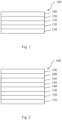
- FIG. 1 is a schematic sectional view of an organic electronic device 100, according to an exemplary embodiment of the present invention.
- the organic electronic device 100 includes a substrate 110, an anode layer 120 and a hole injection layer (HIL) 130 which may comprise a compound of formula (I) and a compound of formula (III).
- HIL 130 is disposed on the anode layer 120.
- EML emission layer
- cathode layer 190 are disposed.
- FIG. 2 is a schematic sectional view of an organic electronic device 100, according to an exemplary embodiment of the present invention.
- the organic electronic device 100 includes a substrate 110, an anode layer 120 and a hole injection layer (HIL) 130 which may comprise a compound of formula (I) and a compound of formula (III).
- the HIL 130 is disposed on the anode layer 120.
- a hole transport layer (HTL) 140, an emission layer (EML) 150, an electron transport layer (ETL) 160, an electron injection layer (EIL) 180 and a cathode layer 190 are disposed.
- EML emission layer
- ETL electron transport layer
- EIL electron injection layer
- FIG. 3 is a schematic sectional view of an organic electronic device (100), according to an exemplary embodiment of the present invention.
- the organic electronic device (100) includes a substrate (110), an anode layer (120) that comprises a first anode sub-layer (121) and a second anode sub-layer (122) and a hole injection layer (HIL) (130).
- the HIL (130) is disposed on the anode layer (120).
- a first emission layer (EML) (150), and a cathode layer (190) are disposed.
- FIG. 4 is a schematic sectional view of an organic electronic device (100), according to an exemplary embodiment of the present invention.
- the organic electronic device (100) includes a substrate (110), an anode layer (120) that comprises a first anode sub-layer (121), a second anode sub-layer (122) and a third anode sub-layer (123), and a hole injection layer (HIL) (130).
- the HIL (130) is disposed on the anode layer (120) comprising a first anode sub-layer (121), a second anode sub-layer (122) and a third anode sub-layer (123).
- a first emission layer (EML) (150), and a cathode layer (190) are disposed.
- FIG. 5 is a schematic sectional view of an organic electronic device (100), according to an exemplary embodiment of the present invention.
- the organic electronic device (100) includes a substrate (110), an anode layer (120) that comprises a first anode sub-layer (121) and a second anode sub-layer (122), and a hole injection layer (HIL) (130).
- the HIL (130) is disposed on the anode layer (120).
- an hole transport layer (HTL) 140
- EML electron transport layer
- BL hole blocking layer
- ETL electron transport layer
- cathode layer 190
- FIG. 6 is a schematic sectional view of an organic electronic device (100), according to an exemplary embodiment of the present invention.
- the organic electronic device (100) includes a substrate (110), an anode layer (120) that comprises a first anode sub-layer (121), a second anode sub-layer (122) and a third anode sub-layer (123), and a hole injection layer (HIL) (130).
- the HIL (130) is disposed on the anode layer (120).
- an hole transport layer (HTL) 140
- EML electron transport layer
- HBL electron transport layer
- cathode layer 190
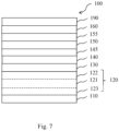
- FIG. 7 is a schematic sectional view of an organic electronic device (100), according to an exemplary embodiment of the present invention.
- the organic electronic device (100) includes a substrate (110), an anode layer (120) that comprises a first anode sub-layer (121) and a second anode sub-layer (122) and a hole injection layer (HIL) (130).
- the HIL (130) is disposed on the anode layer (120).
- a hole transport layer (HTL) (140), an electron blocking layer (EBL) (145), a first emission layer (EML) (150), a hole blocking layer (HBL) (155), an electron transport layer (ETL) (160), and a cathode layer (190) are disposed.
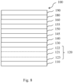
- FIG. 8 is a schematic sectional view of an organic electronic device (100), according to an exemplary embodiment of the present invention.
- the organic electronic device (100) includes a substrate (110), an anode layer (120) that comprises a first anode sub-layer (121), a second anode sub-layer (122) and a third anode sub-layer (123), and a hole injection layer (HIL) (130).
- the HIL (130) is disposed on the anode layer (120).
- HIL hole transport layer
- EBL electron blocking layer
- EML first emission layer
- HBL hole blocking layer
- ETL electron transport layer
- EIL electron injection layer
- a capping and/or a sealing layer may further be formed on the cathode layer 190, in order to seal the organic electronic device 100.
- various other modifications may be applied thereto.
- the invention is furthermore illustrated by the following examples which are illustrative only and non-binding.
- the protonated form of the ligand of formula (II) L-H may be prepared by methods known in the art.
- the HOMO and LUMO energy levels of the molecular structures are determined by applying the hybrid functional B3LYP with a Def2-TZVP basis set and the Stuttgart/Dresden (SDD) effective core potential (ECP) for the metals from the optimized geometries obtained by applying the functional BP86 with a Def2-SVP basis set the Stuttgart/Dresden (SDD) effective core potential (ECP) for the metals.
- SDD Stuttgart/Dresden
- ECP effective core potential
- the HOMO and LUMO energy levels of the molecular structures are determined by applying the hybrid functional B3LYP with a SARC-ZORA-TZVP basis set for the metals and a ZORA-Def2-TZVP basis set for all other atoms from the optimized geometries obtained by applying the functional BP86 with a with a SARC-ZORA-TZVP basis set for the metals and a ZORA-Def2-SVP basis set for all other atoms. All the calculations were performed in the gas phase. All relativistic calculations were performed applying the zero order regular approximation (ZORA). If more than one conformation is viable, the conformation with the lowest total energy is selected.
- ZORA zero order regular approximation
- multiplicities may be applied.
- the multiplicity is shown in brackets: Cu 2+ (doublet), Fe 2+ (quintet), Fe 3+ (sextet), Ce 4+ (singlet).
- the energy of the molecular orbitals (HOMO / LUMO) of compounds of formula of compounds of formula (III), (IV) and (V) were calculated with the program package ORCA V5.0.3 (Max Planck Institute für Kohlenforschung, Kaiser Wilhelm Platz 1, 45470, Muelheim/Ruhr, Germany) and WEASEL 1.9.2 (FAccTs GmbH, Rolandstrasse 67, 50677 German, Germany).
- the HOMO and LUMO energy levels of the molecular structures are determined by applying the hybrid functional B3LYP with a Def2-TZVP basis set from the optimized geometries obtained by applying the functional BP86 with a Def2-SVP basis set in the gas phase. If more than one conformation is viable, the conformation with the lowest total energy is selected.
- the melting point (mp) is determined as peak temperatures from the DSC curves of the above TGA-DSC measurement or from separate DSC measurements (Mettler Toledo DSC822e, heating of samples from room temperature to completeness of melting with heating rate 10 K/min under a stream of pure nitrogen. Sample amounts of 4 to 6 mg are placed in a 40 ⁇ L Mettler Toledo aluminum pan with lid, a ⁇ 1 mm hole is pierced into the lid).
- the glass transition temperature (Tg) is measured under nitrogen and using a heating rate of 10 K per min in a Mettler Toledo DSC 822e differential scanning calorimeter as described in DIN EN ISO 11357, published in March 2010.
- the decomposition temperature T dec is measured by loading a sample of 9 to 11 mg into a Mettler Toledo 100 ⁇ L aluminum pan without lid under nitrogen in a Mettler Toledo TGA-DSC 1 machine. The following heating program was used: 25°C isothermal for 3 min; 25°C to 600°C with 10 K/min.
- the decomposition temperature was determined based on the onset of the decomposition in TGA.
- the decomposition temperature indicates the temperature at which the compound decomposes. The higher the decomposition temperature the higher the thermal stability of a compound.
- the rate onset temperature is determined by loading 100 mg compound into a VTE source.
- VTE source a point source for organic materials may be used as supplied by Kurt J. Lesker Com-pany (www.lesker.com) or CreaPhys GmbH (http://www.creaphys.com).
- the VTE source is heated at a constant rate of 15 K/min at a pressure of less than 10 -5 mbar and the temperature inside the source measured with a thermocouple. Evaporation of the compound is detected with a QCM detector which detects deposition of the compound on the quartz crystal of the detector. The deposition rate on the quartz crystal is measured in ⁇ ngstrom per second. To determine the rate onset temperature, the deposition rate is plotted against the VTE source temperature. The rate onset is the temperature at which noticeable deposition on the QCM detector occurs. For accurate results, the VTE source is heated and cooled three time and only results from the second and third run are used to determine the rate onset temperature.
- the rate onset temperature may be in the range of 200 to 300 °C. If the rate onset temperature is substantially below 200 °C the evaporation may be too rapid and therefore difficult to control. If the rate onset temperature is above 300 °C the evaporation rate may be too low which may result in low tact time and decomposition of the compound of formula (I) and/or compound of formula (III) in VTE source may occur due to prolonged exposure to elevated temperatures.
- the rate onset temperature is an indirect measure of the volatility of a compound. The higher the rate onset temperature the lower is the volatility of a compound.
- a glass substrate with an anode layer comprising a first anode sub-layer of 120 nm Ag, a second anode sub-layer of 8 nm ITO and a third anode sub-layer of 10 nm ITO was cut to a size of 50 mm x 50 mm x 0.7 mm, ultrasonically washed with water for 60 minutes and then with isopropanol for 20 minutes.
- the liquid film was removed in a nitrogen stream, followed by plasma treatment to prepare the anode layer.
- the plasma treatment was performed in an atmosphere comprising 97.6 vol.-% nitrogen and 2.4 vol.-% oxygen.
- HIL hole injection layer
- compound of formula (III) was vacuum deposited on the HIL, to form a HTL having a thickness of 123 nm.
- the compound of formula (III) in the HTL is selected the same as the compound of formula (III) in the HIL.
- the compound of formula (III) can be seen in Table 4.
- N,N-di([1,1'-biphenyl]-4-yl)-3'-(9H-carbazol-9-yl)-[1,1 '-biphenyl]-4-amine was vacuum deposited on the HTL, to form an electron blocking layer (EBL) having a thickness of 5 nm.
- EBL electron blocking layer
- the emission layer (EML) was formed on the EBL having a thickness of 20 nm by co-depositing 99 vol.-% EML host compound BH9 and 1 vol.-% EML dopant BD8.
- a hole blocking layer was formed with a thickness of 5 nm by depositing 4-([1,1'-biphenyl]-4-yl)-6-(3'-(9,9-dimethyl-9H-fluoren-4-yl)-[1,1'-biphenyl]-4-yl)-2-phenylpyrimidine on the emission layer EML.
- the electron transport layer having a thickness of 31 nm was formed on the hole blocking layer by depositing 50 wt.-% 6,6'-(naphthalene-1,2-diylbis(4,1-phenylene))bis(2,4-diphenyl-1,3,5-triazine) and 50 wt.-% of LiQ.
- an electron injection layer was formed on the electron transport layer by depositing a layer of 1.3 nm Yb.
- Ag:Mg (90:10 vol.-%) was evaporated at a rate of 0.01 to 1 ⁇ /s at 10 -7 mbar to form a cathode layer with a thickness of 13 nm on the electron transporting layer.
- N-([1,1'-biphenyl]-4-yl)-9,9-dimethyl-N-(4-(9-phenyl-9H-carbazol-3-yl)phenyl)-9H-fluoren-2-amine was deposited on the cathode layer to form a capping layer with a thickness of 75 nm.
- the OLED stack is protected from ambient conditions by encapsulation of the device with a glass slide. Thereby, a cavity is formed, which includes a getter material for further protection.
- the current efficiency is measured at 20°C.
- the current-voltage characteristic is determined using a Keithley 2635 source measure unit, by sourcing a voltage in V and measuring the current in mA flowing through the device under test. The voltage applied to the device is varied in steps of 0.1V in the range between 0V and 10V.
- the luminance-voltage characteristics and CIE coordinates are determined by measuring the luminance in cd/m 2 using an Instrument Systems CAS-140CT array spectrometer (calibrated by Deutsche Ak relie für sstelle (DAkkS)) for each of the voltage values.
- U(100h)-(1h) To determine the voltage stability over time U(100h)-(1h), a current density of at 20 mA/cm 2 was applied to the device. The operating voltage was measured after 1 hour and after 100 hours, followed by calculation of the voltage stability for the time period of 1 hour to 100 hours. A low value for U(100h)-(1h) denotes a low increase in operating voltage over time and thereby improved voltage stability.
- Table 1 are shown the calculated LUMO in electron volt of compounds of formula (I). The following multiplicities were applied dependent on metal cation: Cu 2+ (doublet), Fe 2+ (quintet), Fe 3+ (sextet), Ce 4+ (singlet).
- Table 1 LUMO values of compounds of formula (I) and comparative compounds Referred to as: Structure LUMO (eV) Comparative compound 4 (CC-4) -3.73 Comparative compound 5 (CC-5) -2.62 Comparative compound 6 (CC-6) -4.02 A1 -4.40 A2 -4.73 A3 -4.92 A4 -4.25 A5 -5.06 A6 -4.50 A7 -4.82 A8 -4.18 A9 -4.53 A10 -4.47 A11 -3.08 A12 -3.62 A13 -3.96 A14 -3.47 A15 -4.20 A16 -3.44 A17 -3.79 A18 -3.05 A19 -3.63 A20 -3.38 A21 -5.16 A22 -5.35 A23 -4.62 A24 -5.54 A25 -4.86 A26 -5.23 A27 -4.55 A28 -4.96 A29 -4.90 A30 -4.48 A31 -5.54 A32
- the compound comprises a Cu(II) cation and a ligand which is free of CF 3 groups.
- the LUMO is -3.73 eV.
- the compound comprises a Fe(II) cation and a ligand which is free of CF 3 groups.
- the LUMO is -2.62 eV.
- the compound comprises a Fe(III) cation and a ligand which is free of CF 3 groups.
- the LUMO is -4.02 eV.
- a LUMO level further away from vacuum level may be beneficial for improved performance of organic electronic devices.
- the LUMO of comparative compound 1 (CC-1) is -3.76 eV.
- the rate onset temperature is 187 °C.
- Comparative compound 3 comprises a different ligand compared to CC-2.
- the LUMO is further improved to -4.76 eV.
- the melting point and rate onset temperature are substantially reduced.
- Compound 1 (A1) comprises a different ligand compared to CC-1.
- the LUMO is -4.4 eV.
- the LUMO is further away from vacuum level. Additionally, the thermal properties are substantially improved compared to comparative compounds 1 to 3.
- Compound 3 (A27), the Fe(II) cation has been replaced by a Fe(III) cation compared to Compound 2. Additionally, Compound 3 comprises a different R 5 group.
- the LUMO is -4.55 eV. Compared to CC-7, the LUMO is further away from vacuum level. The thermal properties are improved substantially compared to comparative compounds 1 to 3, see Table 2.
- compounds of formula (I) may have a LUMO energy in the range suitable for organic electronic devices and/or thermal properties which enable mass production of organic electronic devices.
- Table 3 are shown the properties of compounds of formula (III), in particular molecular mass, HOMO energy, glass transition temperature T g , and rate onset temperature T RO .
- Table 4 are shown characteristics of organic electronic devices comprising a semiconductor layer comprising compounds of formula (I) and comparative compounds CC-1 and CC-2.
- the hole injection layer comprises 7.5 wt.-% CC-1 and 92.5 wt.-% compound of formula (III) K16.
- the operating voltage is 3.45 V
- the U(100h)-(1h) is 0.747 V.
- the hole injection layer comprises 12.5 wt.-% CC-1 and 87.5 wt.-% compound of formula (III) K16.
- the operating voltage is improved to 3.43 V
- the U(100h)-(1h) is improved to 0.630 V.
- the hole injection layer comprises 7.5 wt.-% CC-2 and 92.5 wt.-% compound of formula (III) K16.
- CC-2 differs from CC-1 in the metal cation.
- the operating voltage is 3.46 V, and the U(100h)-(1h) is increased to 0.951 V compared to comparative example 1-1.
- the hole injection layer comprises 12.5 wt.-% CC-2 and 87.5 wt.-% compound of formula (III) K16.
- the operating voltage is improved to 3.44 V
- the U(100h)-(1h) is improved to 0.657 V compared to comparative example 1-3.
- the hole injection layer comprises 6 wt.-% compound of formula (I) A1 and 94 wt.-% comparative HTM-1.
- the operating voltage is 3.41 V
- the U(100h)-(1h) is 0.153 V.
- Example 1-1 the semiconductor layer comprises 6 wt.-% compound of formula (I) A1.
- A1 differs from CC-1 in the ligand.
- Table 4 the operating voltage is improved to 3.33 V and the U(100h)-(1h) is improved to 0.047 V compared to comparative examples 1-1 to 1-5.
- the hole injection layer comprises compound of formula (I) A1 at higher concentrations.
- Table 4 the operating voltage and the U(100h)-(1h) are improved over comparative examples 1-1 to 1-5.
- the hole injection layer comprises 8 wt.-% compound of formula (I) A11.
- A11 differs from A1 in the metal cation.
- the operating voltage is improved to 3.33 V and the U(100h)-(1h) is improved to 0.048 V compared to comparative examples 1-1 to 1-5.
- the hole injection layer comprises compound of formula (I) A11 at higher concentrations.
- Table 4 the operating voltage and the U(100h)-(1h) are improved over comparative examples 1-1 to 1-5.
- the hole injection layer comprises compound of formula (I) A11 and compound of formula (III) K7 at various concentrations.
- the HOMO of K7 is further away from vacuum level compared to K16, see Table 3.
- Table 4 the operating voltage and the U(100h)-(1h) are improved over comparative examples 1-1 to 1-5.
- the hole injection layer comprises compound of formula (I) A1 and compound of formula (III) K18 at two concentrations.
- the HOMO of K18 is closer to vacuum level compared to K16, see Table 3.
- Table 4 the operating voltage and the U(100h)-(1h) are improved over comparative examples 1-1 to 1-5.
- a low operating voltage may be important for low power consumption in organic electronic devices, in particular in mobile devices.
- a low voltage rise over time U(100h)-(1h) may be important for long-term stability operational stability of organic electronic devices.
- Table 2 Properties of compounds of formula (I) and comparative compounds 1 to 3 Referred to as: Structure LUMO (eV) mp (°C) Tg (°C) T dec (°C) T RO (°C) Comparative compound 1 (CC-1) -3.76 n.o. 1) n.d. 2) n.d. 187 Comparative compound 2 (CC-2) -4.14 302 n.o. 308 196 Comparative compound 3 (CC-3) -4.76 158 44 n.d. 97 Compound 1 (A1) -4.40 442 n.d.
Landscapes
- Physics & Mathematics (AREA)
- Optics & Photonics (AREA)
- Electroluminescent Light Sources (AREA)
Priority Applications (5)
| Application Number | Priority Date | Filing Date | Title |
|---|---|---|---|
| EP23162914.8A EP4436334A1 (fr) | 2023-03-20 | 2023-03-20 | Couche d'injection de trous comprenant un composé de formule (i) et un composé de formule (iii) |
| KR1020257031423A KR20250166910A (ko) | 2023-03-20 | 2024-03-19 | 기판, 애노드층, 캐소드층, 적어도 하나의 제1 방출층, 및 정공 주입층을 포함하는 유기 전자 장치 |
| CN202480020336.6A CN120898553A (zh) | 2023-03-20 | 2024-03-19 | 包括基底、阳极层、阴极层、至少一个第一发光层和空穴注入层的有机电子器件 |
| EP24711592.6A EP4684612A1 (fr) | 2023-03-20 | 2024-03-19 | Dispositif électronique organique comprenant un substrat, une couche d'anode, une couche de cathode, au moins une première couche d'émission et une couche d'injection de trous |
| PCT/EP2024/057354 WO2024194322A1 (fr) | 2023-03-20 | 2024-03-19 | Dispositif électronique organique comprenant un substrat, une couche d'anode, une couche de cathode, au moins une première couche d'émission et une couche d'injection de trous |
Applications Claiming Priority (1)
| Application Number | Priority Date | Filing Date | Title |
|---|---|---|---|
| EP23162914.8A EP4436334A1 (fr) | 2023-03-20 | 2023-03-20 | Couche d'injection de trous comprenant un composé de formule (i) et un composé de formule (iii) |
Publications (1)
| Publication Number | Publication Date |
|---|---|
| EP4436334A1 true EP4436334A1 (fr) | 2024-09-25 |
Family
ID=85704653
Family Applications (1)
| Application Number | Title | Priority Date | Filing Date |
|---|---|---|---|
| EP23162914.8A Pending EP4436334A1 (fr) | 2023-03-20 | 2023-03-20 | Couche d'injection de trous comprenant un composé de formule (i) et un composé de formule (iii) |
Country Status (1)
| Country | Link |
|---|---|
| EP (1) | EP4436334A1 (fr) |
Citations (4)
| Publication number | Priority date | Publication date | Assignee | Title |
|---|---|---|---|---|
| EP2722908A1 (fr) | 2012-10-17 | 2014-04-23 | Novaled AG | Diode électroluminescente organique phosphorescente et matières de transport de trous pour diodes électroluminescentes phosphorescentes |
| EP3883003A1 (fr) * | 2020-03-20 | 2021-09-22 | Novaled GmbH | Dispositif électronique organique comprenant un substrat, une couche d'anode, une couche de cathode, au moins une première couche d'émission et une couche d'injection de trous qui comprend un complexe métallique |
| JP2022045366A (ja) * | 2020-09-09 | 2022-03-22 | 東ソー株式会社 | インダンジオン骨格を有する希土類錯体 |
| WO2022189431A1 (fr) | 2021-03-10 | 2022-09-15 | Credoxys GmbH | Nouveaux complexes de cérium (iv) et leur utilisation dans l'électronique organique |
-
2023
- 2023-03-20 EP EP23162914.8A patent/EP4436334A1/fr active Pending
Patent Citations (4)
| Publication number | Priority date | Publication date | Assignee | Title |
|---|---|---|---|---|
| EP2722908A1 (fr) | 2012-10-17 | 2014-04-23 | Novaled AG | Diode électroluminescente organique phosphorescente et matières de transport de trous pour diodes électroluminescentes phosphorescentes |
| EP3883003A1 (fr) * | 2020-03-20 | 2021-09-22 | Novaled GmbH | Dispositif électronique organique comprenant un substrat, une couche d'anode, une couche de cathode, au moins une première couche d'émission et une couche d'injection de trous qui comprend un complexe métallique |
| JP2022045366A (ja) * | 2020-09-09 | 2022-03-22 | 東ソー株式会社 | インダンジオン骨格を有する希土類錯体 |
| WO2022189431A1 (fr) | 2021-03-10 | 2022-09-15 | Credoxys GmbH | Nouveaux complexes de cérium (iv) et leur utilisation dans l'électronique organique |
Non-Patent Citations (9)
| Title |
|---|
| "CRC Handbook of Chemistry and Physics version", 2008, pages: 12 - 114 |
| AHMEDOVA A ET AL: "2-Acetylindan-1,3-dione and its Cu2+ and Zn2+ complexes as promising sunscreen agents", INTERNATIONAL JOURNAL OF COSMETIC SCIENCE, KLUWER ACADEMIC PUBLISHERS, DORDRECHT, NL, vol. 24, no. 2, 2 May 2002 (2002-05-02), pages 103 - 110, XP071469210, ISSN: 0142-5463, DOI: 10.1046/J.1467-2494.2002.00126.X * |
| AHMEDOVA ET AL: "X-ray and ^5^7Fe Mossbauer study on a Fe(III) complex of 2-acetyl-1,3-indandione", INORGANICA CHIMICA ACTA, ELSEVIER BV, NL, vol. 359, no. 10, 1 July 2006 (2006-07-01), pages 3123 - 3128, XP005512665, ISSN: 0020-1693, DOI: 10.1016/J.ICA.2006.01.011 * |
| AHMEDOVA, ANIFE ET AL., NORG. CHIM. ACTA, vol. 359, no. 10, 2006, pages 3123 - 3128 |
| BACHLAUS M. K. ET AL: "Chelating Tendencies of Some N-(2-Acetyl-1,3-Indandione) Trialkyl Ammonium Iodides with Transition Metal Ions", ZEITSCHRIFT FUR NATURFORSCHUNG - SECTION B JOURNAL OF CHEMICAL SCIENCES, vol. 28, no. 5-6, 1 June 1973 (1973-06-01), DE, pages 317 - 318, XP093065705, ISSN: 0932-0776, DOI: 10.1515/znb-1973-5-618 * |
| E.E.S. TEOTONIO ET AL: "Novel electroluminescent devices containing Eu3+-(2-acyl-1,3-indandionate) complexes with TPPO ligand", OPTICAL MATERIALS, vol. 32, no. 2, 1 December 2009 (2009-12-01), NL, pages 345 - 349, XP055563069, ISSN: 0925-3467, DOI: 10.1016/j.optmat.2009.08.015 * |
| ENCHEV, VENELIN ET AL., J. MOL. STRUCT., vol. 595, no. 1-3, 2001, pages 67 - 76 |
| RUSANOV, VENTZISLAV ET AL., EUR. J. CHEM.,, vol. 5, no. 1, 2014, pages 176 - 180 |
| YASUHIKO SHIROTAHIROSHI KAGEYAMA, CHEM. REV., vol. 107, 2007, pages 953 - 1010 |
Similar Documents
| Publication | Publication Date | Title |
|---|---|---|
| EP4244911B1 (fr) | Dispositif électronique organique comprenant un composé de formule (1), dispositif d'affichage comprenant le dispositif électronique organique, ainsi que composés de formule (1) à utiliser dans des dispositifs électroniques organiques | |
| KR102939047B1 (ko) | Ce(IV) 금속 착물, 및 애노드층, 캐소드층, 및 상기 Ce(IV) 금속 착물을 포함하는 p-형 전하 발생층 및 n-형 전하 발생층을 포함하는 전하 발생층을 포함하는 유기 전자 소자 | |
| EP3989305A1 (fr) | Dispositif électronique organique comprenant un composé de formule (1), dispositif d'affichage comprenant le dispositif électronique organique, ainsi que composés de formule (1) à utiliser dans des dispositifs électroniques organiques | |
| EP4496458A2 (fr) | Complexes métalliques de 3-(2,3,5-trifluoro-6-(trifluorométhyl)pyridin-4-yl)pentane-2,4-dione et ligands similaires en tant que matériaux semi-conducteurs destinés à être utilisés dans des dispositifs électroniques | |
| US20230056322A1 (en) | Organic Electronic Device Comprising a Compound of Formula (I), Display Device Comprising the Organic Electronic Device as Well as Compounds of Formula (I) for Use in Organic Electronic Devices | |
| EP4169086B1 (fr) | Composé organique de formule (i) pour une utilisation dans des dispositifs électroniques organiques, dispositif électronique organique comprenant un composé de formule (i) et dispositif d'affichage comprenant le dispositif électronique organique | |
| EP3883003A1 (fr) | Dispositif électronique organique comprenant un substrat, une couche d'anode, une couche de cathode, au moins une première couche d'émission et une couche d'injection de trous qui comprend un complexe métallique | |
| EP4152426A1 (fr) | Dispositif électronique organique comprenant un substrat, une couche d'anode, une couche de cathode, au moins une première couche d'émission et une couche d'injection de trous comprenant un complexe métallique, ainsi que complexe métallique | |
| US20230006155A1 (en) | Organic Electronic Device Comprising a Compound of Formula (I), Display Device Comprising the Organic Electronic Device as Well as Compounds of Formula (I) for Use in Organic Electronic Devices | |
| EP3840074A1 (fr) | Dispositif électronique organique comprenant un composé de formule (1), dispositif d'affichage comprenant le dispositif électronique organique, ainsi que composés de formule (1) à utiliser dans des dispositifs électroniques organiques | |
| EP4097777B1 (fr) | Dispositif électronique organique comprenant une couche d'anode, une couche de cathode, au moins une couche d'émission (eml) et au moins une couche d'injection par trous (hil) | |
| EP3859808A1 (fr) | Dispositif électronique organique comprenant une couche d'injection de trous incluant un composé de transport de trous | |
| US20240292735A1 (en) | Organic electronic devices comprising metal complexes with high dipole moment fragments | |
| EP4436334A1 (fr) | Couche d'injection de trous comprenant un composé de formule (i) et un composé de formule (iii) | |
| EP4106026A1 (fr) | Dispositif électronique organique comprenant un substrat, une couche d'anode, une couche de cathode, au moins une première couche d'émission et au moins une couche d'injection de trous qui comprend un complexe métallique | |
| EP4518635B1 (fr) | Dispositif électronique organic avec une couche d'injection de trous comprenant un composé de formule (i) et un composé de formule (iii) | |
| EP4434961A1 (fr) | Composé de formule (i), dispositif électronique organique comprenant un composé de formule (i), dispositif d'affichage comprenant le dispositif électronique organique | |
| EP4382510B1 (fr) | Composé de formule (i), dispositif électronique organique comprenant un composé de formule (i), dispositif d'affichage comprenant le dispositif électronique organique | |
| EP4516876B1 (fr) | Composé de formule (i), dispositif électronique organique comprenant un composé de formule (i), dispositif d'affichage comprenant le dispositif électronique organique | |
| EP4406385B1 (fr) | Complexe métallique, couche semi-conductrice comprenant un complexe métallique et dispositif électronique organique | |
| EP4478862A1 (fr) | Dispositif électroluminescent organique comprenant un premier composé métallique et un second composé métallique, et dispositif d'affichage comprenant le dispositif électroluminescent organique | |
| EP4570789A1 (fr) | Composé de formule (i), dispositif électronique organique comprenant un composé de formule (i), dispositif d'affichage comprenant le dispositif électronique organique | |
| EP4340582A1 (fr) | Dispositif électronique organique comprenant une couche de génération de charge | |
| EP4570808A1 (fr) | Composé de formule (i), dispositif électronique organique comprenant un composé de formule (i), dispositif d'affichage comprenant le dispositif électronique organique | |
| EP4684612A1 (fr) | Dispositif électronique organique comprenant un substrat, une couche d'anode, une couche de cathode, au moins une première couche d'émission et une couche d'injection de trous |
Legal Events
| Date | Code | Title | Description |
|---|---|---|---|
| PUAI | Public reference made under article 153(3) epc to a published international application that has entered the european phase |
Free format text: ORIGINAL CODE: 0009012 |
|
| STAA | Information on the status of an ep patent application or granted ep patent |
Free format text: STATUS: THE APPLICATION HAS BEEN PUBLISHED |
|
| AK | Designated contracting states |
Kind code of ref document: A1 Designated state(s): AL AT BE BG CH CY CZ DE DK EE ES FI FR GB GR HR HU IE IS IT LI LT LU LV MC ME MK MT NL NO PL PT RO RS SE SI SK SM TR |
|
| TPAC | Observations filed by third parties |
Free format text: ORIGINAL CODE: EPIDOSNTIPA |
|
| STAA | Information on the status of an ep patent application or granted ep patent |
Free format text: STATUS: REQUEST FOR EXAMINATION WAS MADE |
|
| STAA | Information on the status of an ep patent application or granted ep patent |
Free format text: STATUS: EXAMINATION IS IN PROGRESS |
|
| 17P | Request for examination filed |
Effective date: 20250312 |
|
| 17Q | First examination report despatched |
Effective date: 20250411 |