EP4099383A1 - Faradaykäfig-plastikgehäuse mit vorgespritztem hohlraum-leadframe - Google Patents
Faradaykäfig-plastikgehäuse mit vorgespritztem hohlraum-leadframe Download PDFInfo
- Publication number
- EP4099383A1 EP4099383A1 EP22176372.5A EP22176372A EP4099383A1 EP 4099383 A1 EP4099383 A1 EP 4099383A1 EP 22176372 A EP22176372 A EP 22176372A EP 4099383 A1 EP4099383 A1 EP 4099383A1
- Authority
- EP
- European Patent Office
- Prior art keywords
- lid
- leadframe
- tie bars
- die attach
- faraday cage
- Prior art date
- Legal status (The legal status is an assumption and is not a legal conclusion. Google has not performed a legal analysis and makes no representation as to the accuracy of the status listed.)
- Withdrawn
Links
Images









Classifications
-
- H—ELECTRICITY
- H10—SEMICONDUCTOR DEVICES; ELECTRIC SOLID-STATE DEVICES NOT OTHERWISE PROVIDED FOR
- H10W—GENERIC PACKAGES, INTERCONNECTIONS, CONNECTORS OR OTHER CONSTRUCTIONAL DETAILS OF DEVICES COVERED BY CLASS H10
- H10W42/00—Arrangements for protection of devices
- H10W42/20—Arrangements for protection of devices protecting against electromagnetic or particle radiation, e.g. light, X-rays, gamma-rays or electrons
-
- H—ELECTRICITY
- H10—SEMICONDUCTOR DEVICES; ELECTRIC SOLID-STATE DEVICES NOT OTHERWISE PROVIDED FOR
- H10W—GENERIC PACKAGES, INTERCONNECTIONS, CONNECTORS OR OTHER CONSTRUCTIONAL DETAILS OF DEVICES COVERED BY CLASS H10
- H10W70/00—Package substrates; Interposers; Redistribution layers [RDL]
- H10W70/01—Manufacture or treatment
- H10W70/04—Manufacture or treatment of leadframes
- H10W70/041—Connecting or disconnecting interconnections to or from leadframes, e.g. connecting bond wires or bumps
-
- H—ELECTRICITY
- H10—SEMICONDUCTOR DEVICES; ELECTRIC SOLID-STATE DEVICES NOT OTHERWISE PROVIDED FOR
- H10W—GENERIC PACKAGES, INTERCONNECTIONS, CONNECTORS OR OTHER CONSTRUCTIONAL DETAILS OF DEVICES COVERED BY CLASS H10
- H10W70/00—Package substrates; Interposers; Redistribution layers [RDL]
- H10W70/01—Manufacture or treatment
- H10W70/04—Manufacture or treatment of leadframes
- H10W70/048—Mechanical treatments, e.g. punching, cutting, deforming or cold welding
-
- H—ELECTRICITY
- H10—SEMICONDUCTOR DEVICES; ELECTRIC SOLID-STATE DEVICES NOT OTHERWISE PROVIDED FOR
- H10W—GENERIC PACKAGES, INTERCONNECTIONS, CONNECTORS OR OTHER CONSTRUCTIONAL DETAILS OF DEVICES COVERED BY CLASS H10
- H10W70/00—Package substrates; Interposers; Redistribution layers [RDL]
- H10W70/01—Manufacture or treatment
- H10W70/05—Manufacture or treatment of insulating or insulated package substrates, or of interposers, or of redistribution layers
-
- H—ELECTRICITY
- H10—SEMICONDUCTOR DEVICES; ELECTRIC SOLID-STATE DEVICES NOT OTHERWISE PROVIDED FOR
- H10W—GENERIC PACKAGES, INTERCONNECTIONS, CONNECTORS OR OTHER CONSTRUCTIONAL DETAILS OF DEVICES COVERED BY CLASS H10
- H10W70/00—Package substrates; Interposers; Redistribution layers [RDL]
- H10W70/40—Leadframes
- H10W70/464—Additional interconnections in combination with leadframes
- H10W70/465—Bumps or wires
-
- H—ELECTRICITY
- H10—SEMICONDUCTOR DEVICES; ELECTRIC SOLID-STATE DEVICES NOT OTHERWISE PROVIDED FOR
- H10W—GENERIC PACKAGES, INTERCONNECTIONS, CONNECTORS OR OTHER CONSTRUCTIONAL DETAILS OF DEVICES COVERED BY CLASS H10
- H10W70/00—Package substrates; Interposers; Redistribution layers [RDL]
- H10W70/40—Leadframes
- H10W70/479—Leadframes on or in insulating or insulated package substrates, interposers, or redistribution layers
-
- H—ELECTRICITY
- H10—SEMICONDUCTOR DEVICES; ELECTRIC SOLID-STATE DEVICES NOT OTHERWISE PROVIDED FOR
- H10W—GENERIC PACKAGES, INTERCONNECTIONS, CONNECTORS OR OTHER CONSTRUCTIONAL DETAILS OF DEVICES COVERED BY CLASS H10
- H10W74/00—Encapsulations, e.g. protective coatings
- H10W74/01—Manufacture or treatment
-
- H—ELECTRICITY
- H10—SEMICONDUCTOR DEVICES; ELECTRIC SOLID-STATE DEVICES NOT OTHERWISE PROVIDED FOR
- H10W—GENERIC PACKAGES, INTERCONNECTIONS, CONNECTORS OR OTHER CONSTRUCTIONAL DETAILS OF DEVICES COVERED BY CLASS H10
- H10W74/00—Encapsulations, e.g. protective coatings
- H10W74/40—Encapsulations, e.g. protective coatings characterised by their materials
-
- H—ELECTRICITY
- H10—SEMICONDUCTOR DEVICES; ELECTRIC SOLID-STATE DEVICES NOT OTHERWISE PROVIDED FOR
- H10W—GENERIC PACKAGES, INTERCONNECTIONS, CONNECTORS OR OTHER CONSTRUCTIONAL DETAILS OF DEVICES COVERED BY CLASS H10
- H10W76/00—Containers; Fillings or auxiliary members therefor; Seals
- H10W76/01—Manufacture or treatment
-
- H—ELECTRICITY
- H10—SEMICONDUCTOR DEVICES; ELECTRIC SOLID-STATE DEVICES NOT OTHERWISE PROVIDED FOR
- H10W—GENERIC PACKAGES, INTERCONNECTIONS, CONNECTORS OR OTHER CONSTRUCTIONAL DETAILS OF DEVICES COVERED BY CLASS H10
- H10W76/00—Containers; Fillings or auxiliary members therefor; Seals
- H10W76/10—Containers or parts thereof
- H10W76/12—Containers or parts thereof characterised by their shape
- H10W76/13—Containers comprising a conductive base serving as an interconnection
- H10W76/134—Containers comprising a conductive base serving as an interconnection having other interconnections parallel to the conductive base
-
- H—ELECTRICITY
- H10—SEMICONDUCTOR DEVICES; ELECTRIC SOLID-STATE DEVICES NOT OTHERWISE PROVIDED FOR
- H10W—GENERIC PACKAGES, INTERCONNECTIONS, CONNECTORS OR OTHER CONSTRUCTIONAL DETAILS OF DEVICES COVERED BY CLASS H10
- H10W76/00—Containers; Fillings or auxiliary members therefor; Seals
- H10W76/60—Seals
-
- H—ELECTRICITY
- H10—SEMICONDUCTOR DEVICES; ELECTRIC SOLID-STATE DEVICES NOT OTHERWISE PROVIDED FOR
- H10W—GENERIC PACKAGES, INTERCONNECTIONS, CONNECTORS OR OTHER CONSTRUCTIONAL DETAILS OF DEVICES COVERED BY CLASS H10
- H10W95/00—Packaging processes not covered by the other groups of this subclass
-
- H—ELECTRICITY
- H10—SEMICONDUCTOR DEVICES; ELECTRIC SOLID-STATE DEVICES NOT OTHERWISE PROVIDED FOR
- H10W—GENERIC PACKAGES, INTERCONNECTIONS, CONNECTORS OR OTHER CONSTRUCTIONAL DETAILS OF DEVICES COVERED BY CLASS H10
- H10W70/00—Package substrates; Interposers; Redistribution layers [RDL]
- H10W70/40—Leadframes
- H10W70/421—Shapes or dispositions
-
- H—ELECTRICITY
- H10—SEMICONDUCTOR DEVICES; ELECTRIC SOLID-STATE DEVICES NOT OTHERWISE PROVIDED FOR
- H10W—GENERIC PACKAGES, INTERCONNECTIONS, CONNECTORS OR OTHER CONSTRUCTIONAL DETAILS OF DEVICES COVERED BY CLASS H10
- H10W70/00—Package substrates; Interposers; Redistribution layers [RDL]
- H10W70/40—Leadframes
- H10W70/421—Shapes or dispositions
- H10W70/424—Cross-sectional shapes
-
- H—ELECTRICITY
- H10—SEMICONDUCTOR DEVICES; ELECTRIC SOLID-STATE DEVICES NOT OTHERWISE PROVIDED FOR
- H10W—GENERIC PACKAGES, INTERCONNECTIONS, CONNECTORS OR OTHER CONSTRUCTIONAL DETAILS OF DEVICES COVERED BY CLASS H10
- H10W72/00—Interconnections or connectors in packages
- H10W72/01—Manufacture or treatment
- H10W72/0198—Manufacture or treatment batch processes
-
- H—ELECTRICITY
- H10—SEMICONDUCTOR DEVICES; ELECTRIC SOLID-STATE DEVICES NOT OTHERWISE PROVIDED FOR
- H10W—GENERIC PACKAGES, INTERCONNECTIONS, CONNECTORS OR OTHER CONSTRUCTIONAL DETAILS OF DEVICES COVERED BY CLASS H10
- H10W72/00—Interconnections or connectors in packages
- H10W72/071—Connecting or disconnecting
- H10W72/073—Connecting or disconnecting of die-attach connectors
-
- H—ELECTRICITY
- H10—SEMICONDUCTOR DEVICES; ELECTRIC SOLID-STATE DEVICES NOT OTHERWISE PROVIDED FOR
- H10W—GENERIC PACKAGES, INTERCONNECTIONS, CONNECTORS OR OTHER CONSTRUCTIONAL DETAILS OF DEVICES COVERED BY CLASS H10
- H10W72/00—Interconnections or connectors in packages
- H10W72/071—Connecting or disconnecting
- H10W72/075—Connecting or disconnecting of bond wires
-
- H—ELECTRICITY
- H10—SEMICONDUCTOR DEVICES; ELECTRIC SOLID-STATE DEVICES NOT OTHERWISE PROVIDED FOR
- H10W—GENERIC PACKAGES, INTERCONNECTIONS, CONNECTORS OR OTHER CONSTRUCTIONAL DETAILS OF DEVICES COVERED BY CLASS H10
- H10W72/00—Interconnections or connectors in packages
- H10W72/50—Bond wires
- H10W72/541—Dispositions of bond wires
- H10W72/5445—Dispositions of bond wires being orthogonal to a side surface of the chip, e.g. parallel arrangements
-
- H—ELECTRICITY
- H10—SEMICONDUCTOR DEVICES; ELECTRIC SOLID-STATE DEVICES NOT OTHERWISE PROVIDED FOR
- H10W—GENERIC PACKAGES, INTERCONNECTIONS, CONNECTORS OR OTHER CONSTRUCTIONAL DETAILS OF DEVICES COVERED BY CLASS H10
- H10W72/00—Interconnections or connectors in packages
- H10W72/851—Dispositions of multiple connectors or interconnections
- H10W72/874—On different surfaces
- H10W72/884—Die-attach connectors and bond wires
-
- H—ELECTRICITY
- H10—SEMICONDUCTOR DEVICES; ELECTRIC SOLID-STATE DEVICES NOT OTHERWISE PROVIDED FOR
- H10W—GENERIC PACKAGES, INTERCONNECTIONS, CONNECTORS OR OTHER CONSTRUCTIONAL DETAILS OF DEVICES COVERED BY CLASS H10
- H10W76/00—Containers; Fillings or auxiliary members therefor; Seals
- H10W76/10—Containers or parts thereof
- H10W76/12—Containers or parts thereof characterised by their shape
-
- H—ELECTRICITY
- H10—SEMICONDUCTOR DEVICES; ELECTRIC SOLID-STATE DEVICES NOT OTHERWISE PROVIDED FOR
- H10W—GENERIC PACKAGES, INTERCONNECTIONS, CONNECTORS OR OTHER CONSTRUCTIONAL DETAILS OF DEVICES COVERED BY CLASS H10
- H10W76/00—Containers; Fillings or auxiliary members therefor; Seals
- H10W76/10—Containers or parts thereof
- H10W76/17—Containers or parts thereof characterised by their materials
- H10W76/18—Insulating materials, e.g. resins, glasses or ceramics
-
- H—ELECTRICITY
- H10—SEMICONDUCTOR DEVICES; ELECTRIC SOLID-STATE DEVICES NOT OTHERWISE PROVIDED FOR
- H10W—GENERIC PACKAGES, INTERCONNECTIONS, CONNECTORS OR OTHER CONSTRUCTIONAL DETAILS OF DEVICES COVERED BY CLASS H10
- H10W90/00—Package configurations
- H10W90/701—Package configurations characterised by the relative positions of pads or connectors relative to package parts
- H10W90/731—Package configurations characterised by the relative positions of pads or connectors relative to package parts of die-attach connectors
- H10W90/736—Package configurations characterised by the relative positions of pads or connectors relative to package parts of die-attach connectors between a chip and a stacked lead frame, conducting package substrate or heat sink
-
- H—ELECTRICITY
- H10—SEMICONDUCTOR DEVICES; ELECTRIC SOLID-STATE DEVICES NOT OTHERWISE PROVIDED FOR
- H10W—GENERIC PACKAGES, INTERCONNECTIONS, CONNECTORS OR OTHER CONSTRUCTIONAL DETAILS OF DEVICES COVERED BY CLASS H10
- H10W90/00—Package configurations
- H10W90/701—Package configurations characterised by the relative positions of pads or connectors relative to package parts
- H10W90/751—Package configurations characterised by the relative positions of pads or connectors relative to package parts of bond wires
- H10W90/754—Package configurations characterised by the relative positions of pads or connectors relative to package parts of bond wires between a chip and a stacked insulating package substrate, interposer or RDL
-
- H—ELECTRICITY
- H10—SEMICONDUCTOR DEVICES; ELECTRIC SOLID-STATE DEVICES NOT OTHERWISE PROVIDED FOR
- H10W—GENERIC PACKAGES, INTERCONNECTIONS, CONNECTORS OR OTHER CONSTRUCTIONAL DETAILS OF DEVICES COVERED BY CLASS H10
- H10W90/00—Package configurations
- H10W90/701—Package configurations characterised by the relative positions of pads or connectors relative to package parts
- H10W90/751—Package configurations characterised by the relative positions of pads or connectors relative to package parts of bond wires
- H10W90/756—Package configurations characterised by the relative positions of pads or connectors relative to package parts of bond wires between a chip and a stacked lead frame, conducting package substrate or heat sink
Definitions
- the present invention relates generally to integrated circuits, and more particularly to a Faraday cage plastic cavity package with a pre-molded cavity leadframe.
- Flat no-leads packages such as QFN (quad-flat no-leads) and DFN (dual-flat no-leads) are used to physically and electrically connect integrated circuits to printed circuit boards.
- Two types of flat no-leads packages are common: cavity (i.e. with a cavity designed into the package containing air or nitrogen), and plastic-molded (i.e. with minimal air in the package).
- the cavity package is usually made up of three parts; a copper leadframe, plastic-molded body (open, and not sealed), and a cap or lid attached to the plastic portion of the leadframe.
- An integrated circuit (IC) is mounted to a die attach pad within the cavity, with wire leads connecting the IC to the leadframe.
- the leadframe terminates in contacts on the bottom of the package for providing electrical interconnection with a printed circuit board.
- Cavity packages are small and lightweight, with good thermal and electrical performance that makes them suitable for portable communication / consumer products.
- Applications include cellular phones, PDAs, wireless transmitters, RF front end, HD devices, microcontrollers, pre-amplifiers, servers, smart power suppliers, switches, DSPs, ASICs and wrist watches.
- US Patents 9,257,370 and 9,536,812 both disclose a metal ring that is integrated into the pre-molded cavity leadframe.
- the metal ring provides an electrical ground path from the metal cap to the die attach pad and permits attachment of the metal cap to the pre-molded leadframe using solder reflow onto.
- These patents both disclose traditional cavity packages with pre-molded leadframes useful for protecting sensitive integrated circuit dies from hazardous environments.
- These cavity packages with pre-molded leadframes also provide a format for such dies to be easily handled and directly attached onto external circuits such as printed circuit boards.
- a Faraday cage plastic cavity package with a pre-molded cavity leadframe is provided, as set forth in the specification below and the attached drawings.
- the present system provides a Faraday cage cavity package, comprising: (a) a leadframe having a die attach paddle, tie bars extending outwardly from the die attach paddle, and lead fingers positioned between the tie bars; (b) a body molded to the leadframe forming a cavity exposing top surfaces of the die attach paddle, the tie bars and the lead fingers within the cavity; (c) a die attached to the die attach pad by wire bonding to the lead fingers; and (d) a lid attached onto the top of the leadframe, the lid having an electrically conductive portion in electrical contact with the tie bars.
- connecting leads may be attached onto the tie bars, and the plastic molding does not cover these connecting leads. These connecting leads may be connecting leads solder balls connected by solder reflow.
- the molding may be performed such that there are additional cavities over the distal ends of the tie bars, and these additional cavities can be filled with conductive materials.
- the tie bars may have design pads formed thereon (within the cavity) and be in contact with an electrically conductive coating on the bottom end portions of the lid.
- the lid may be a metal lid, or a plastic lid with an electrically conductive coating. To assist in mounting the bottom of the present Faraday cage cavity package to a printed circuit board, portions of the bottom surfaces of the die attach paddle and the lead fingers may be plated for surface mount reflow, while other portions may be oxidized to resist solder wetting.
- a system for manufacturing a Faraday cage cavity package comprising: (a) fabricating a matrix of leadframes, each leadframe in the matrix having: a die attach paddle, tie bars extending outwardly from the die attach paddle, and lead fingers positioned between the tie bars; (b) molding plastic onto the matrix of leadframes, wherein the molding the plastic comprises forming a cavity in each leadframe exposing portions of top surfaces of the die attach paddle, the tie bars and the lead fingers within the cavity; (c) attaching a die to the die attach paddle on each leadframe by wire bonding the die to the lead fingers; (d) attaching a lid onto the top of each leadframe, the lid having an electrically conductive portion in electrical contact with the tie bars; and then (e) separating the matrix of leadframes into a plurality of individual Faraday cage cavity package units.
- connecting leads may be attached onto the tie bars prior to molding the plastic onto the matrix of leadframes, or additional cavities may be formed at the distal ends of the tie bars and then filled with conductive materials, or the tie bars may have design pads thereon which are then connected to the lid.
- the lid may be a metal lid or a plastic lid with electrically conductive coatings thereon. Bottom surfaces of the die attach paddle and the lead fingers may be soldered to an external circuit such as a printed circuit board.
- the present Faraday cage cavity packages are manufactured in a matrix format, and then are then separated into a plurality of individual Faraday cage cavity package units by saw singulation.
- a prior art cavity package 10 is shown with a pre-molded cavity leadframe, as illustrated in US Patents 9,257,370 and 9,536,812 .
- Package 10 includes a metal seal ring 11, exposed lead fingers 12 for wire bonding, and a die attach pad (DAP) 13.
- DAP die attach pad
- FIG. 1C the top sides of metal seal ring 11, lead fingers 12 and DAP 13 are all exposed (and can be seen when lid 14 ( FIGS.1 A and 1B ) is removed.
- a molded plastic body 15 is formed onto the device. The bottom of the DAP 13 is seen in FIG. 1B .
- Element 16 is the leadframe that is molded within plastic body 15 to form the device.
- the present system employs manufacturing techniques and mechanical parts somewhat similar to those described in US Patents 9,257,370 and 9,536,812 , and these patents are accordingly incorporated herein by reference in their entireties for all purposes. Importantly, however, the present system produces a novel and non-obvious Faraday cage which is not seen in US Patents 9,257,370 and 9,536,812 .
- FIG. 2 is a flowchart showing steps in a first exemplary method 100 for constructing a Faraday cage plastic cavity package with a pre-molded cavity leadframe, as illustrated in FIGS. 3 to 8 .
- Method 100 comprises the following steps:
- a matrix format for manufacturing leadframes 50 is simply a repeating pattern of individual leadframes 50 all connected together. Further explanations of using a matrix to manufacture leadframes is set forth in US Patents 9,257,370 and 9,536,812 incorporated herein by reference in their entireties for all purposes.
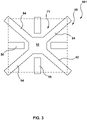
- FIG. 3 shows details at Step 101 of the process 100 set forth in FIG. 2 to fabricate a leadframe 50 in a matrix format (with only one leadframe 50 illustrated for clarity).
- FIG. 4 shows details at Step 102 of the process 100 set forth in FIG. 2 , including a cross-section through A-A.
- connecting leads 60 e.g solder balls
- FIG. 5 shows details at Step 103 of the process 100 set forth in FIG. 2 , including a cross-section through A-A, for molding a plastic body 70 onto leadframe 50 to form at least a cavity 71 in which part of fingers 56's top and bottom surfaces are exposed, the DAP 52's top and bottom surfaces are exposed, and the top side of tie bars 54 are exposed.
- the tops of connecting leads (e.g.: solder balls) 60 are also exposed after the molding of plastic body 70 over leadframe 50.
- FIG. 6 shows details at Step 104 of the process 100 set forth in FIG. 2 , including a cross-section through B-B, where die 80 is attached onto the top of DAP 52 with bonding wires 82 connected to fingers 56.
- FIG. 7 shows details at Step 105 of the process 100 set forth in FIG. 2 .
- a lid is fabricated.
- Lid 90A, or 90B or 90C is fabricated with an electrically conductive surface, and may be a metal lid 90A, a plastic lid 90B with electrical conducting coating on its entire surface, or a plastic lid 90C with electrical conducting coating only on its internal and bottom surfaces, 91 and 92 respectively.
- FIG. 8 shows details at Step 106 of the process 100 set forth in FIG. 2 in which lid 90 (90A, 90B or 90C) is attached onto the top of the cavity leadframe 50 by electrically conductive material/s.
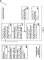
- FIG. 9 is flowchart showing steps in a second exemplary method 200 for constructing a Faraday cage plastic cavity package with a pre-molded cavity leadframe, as illustrated in FIGS. 10 to 15 .
- Method 200 comprises the following steps:
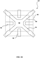
- FIG. 10 shows details at Step 201 of the process 200 set forth in FIG. 9 to fabricate a leadframe in a matrix format (with only one leadframe 50 illustrated for clarity).
- FIG. 11 shows details at Step 202 of the process 200 set forth in FIG. 9 , including a cross section through A-A, for molding a plastic body 70 onto leadframe 50 to form at least a center cavity 71 in which part of fingers 56's top and bottom surfaces are exposed, and cavities 72 above the distal ends of tie bars 54 are also exposed.
- center cavity 71 the DAP 52's top and bottom surfaces are exposed, and the top sides of the center portions of tie bars 54 are also exposed.
- FIG. 12 shows details at Step 203 of the process 200 set forth in FIG. 9 , including a cross-section through B-B, where die 80 is attached onto the top of DAP 52 with bonding wires 82 connected to fingers 56.
- FIG. 13 shows details at Step 204 of the process 200 set forth in FIG. 9 , including a cross-section through A-A, in which an adequate amount of conductive material is dispensed into cavities 72 in which the top side of the connecting lead/s to the DAP 52 are exposed.
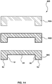
- FIG. 14 shows details at Step 205 of the process 100 set forth in FIG. 2 .
- a lid is fabricated.
- Lid 90A, or 90B or 90C is fabricated with an electrically conductive surface, and may be a metal lid 90A, a plastic lid 90B with electrical conducting coating on its entire surface, or a plastic lid 90C with electrical conducting coating only on its internal and bottom surfaces, 91 and 92 respectively.
- FIG. 15 shows details at Step 206 of the process 200 set forth in FIG. 9 , including a cross-sections through A-A and B-B, showing details which lid 90 (90A, 90B or 90C) is attached onto the top of the cavity leadframe 50 by electrically conductive materials.
- Lid 90 may be connected to body 70 by electrically conductive adhesives.
- FIG. 16 is a flowchart showing steps in a third exemplary method 300 for constructing a Faraday cage plastic cavity package with a pre-molded cavity leadframe, as illustrated in FIGS. 17 to 21 .
- Method 300 comprises the following steps:
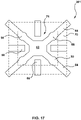
- FIG. 17 shows details at Step 301 of the process 300 set forth in FIG. 16 to fabricate a leadframe in a matrix format (with only one leadframe 50 illustrated for clarity).
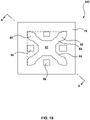
- FIG. 18 shows details at Step 302 of the process 300 set forth in FIG. 16 for molding a plastic body 70 onto leadframe 50 to form at least a center cavity 71 in which part of fingers 56's top and bottom surfaces are exposed, and design pads 55 on tie bars 54 are also exposed.
- center cavity 71 the DAP 52's top and bottom surfaces are exposed, and the top sides of the center portions of tie bars 54 are also exposed.
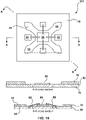
- FIG. 19 shows details at Step 303 of the process 300 set forth in FIG. 16 , including cross-sections through A-A and B-B, where die 80 is attached onto the top of DAP 52 with bonding wires 82 connected to fingers 56.
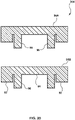
- FIG. 20 shows details at Step 304 of the process 300 set forth in FIG. 16 to fabricate a lid 95A or 95B with bottom protrusions 96 thereon.
- Lid 95A or 95B is fabricated with an electrically conductive surface, and may be a metal lid 95A, or a plastic lid 95B with electrical conducting coating on its entire surface or its internal and bottom surfaces, 91 and 92 respectively. wherein at least the internal surface surface of the cap and protrusion/s are covered by electrical conductive material, including option d) of a plastic lid with electrical conducted coating on its entire surface, or option e) of a plastic lid with electrical conducted coating on its internal & bottom surface.
- FIG. 21 shows details at Step 305 of the process 300 set forth in FIG. 16 , including a cross-section through A-A, showing details which lid 95 (95A or 95B) is attached onto the top of the cavity leadframe 50 by electrically conductive materials.
- lid 95 95A or 95B
- bottom protrusions 96 may be in electrical contact with fingers 96 while lid 95 may be connected to body 70 by electrically conductive adhesives.
- the present system further includes a method of manufacturing a Faraday cage cavity package, comprising: fabricating a matrix of leadframes 50, each leadframe 50 in the matrix having: a die attach paddle 52, tie bars 54 extending outwardly from die attach paddle 52, and lead fingers 56 positioned between tie bars 54; molding a (preferably plastic) body 70 onto the matrix of leadframes 50, wherein the molding the plastic comprises forming a cavity 71 in each leadframe 50 exposing portions of top surfaces of the die attach paddle 52, tie bars 54 and lead fingers 56 within the cavity; attaching a die 80 to die attach paddle 52 by wire bonding die 80 to lead fingers 56; attaching a lid 90 or 95 onto the top of each leadframe 50, the lid having an electrically conductive portion in electrical contact with tie bars 54; and then separating the matrix of leadframes into a plurality of individual Faraday cage cavity package units.
- connecting leads 60 are attached onto tie bars 54 prior to molding the plastic body 70 onto the matrix of leadframes.
- additional cavities 72 may be formed over the distal ends of tie bars 54. Cavities 72 may be filled with a conductive material, and then electrically connecting the lid 90 or 95 to the conductive material in cavities 72.
- tie bars 54 have design pads 55 thereon, and design pads 55 are not covered by the molded plastic during the molding process. Design pads 55 can be disposed within cavity 71. Lid 90 or 95 has a bottom end portion with an electrically conductive coating thereon in contact with the design pads.
- the bottom surfaces of die attach paddle 52 and lead fingers 54 are exposed and are soldered to an external circuit.
- first portions of the bottom surfaces of the die attach paddle and the lead fingers are plated for surface mount reflow, and second portions of the bottom surfaces of the die attach paddle and the lead fingers are oxidized to resist solder wetting.
- the leadframe 50 is made of metal and the molded body 70 is made of plastic.
Landscapes
- Lead Frames For Integrated Circuits (AREA)
- Engineering & Computer Science (AREA)
- Ceramic Engineering (AREA)
- Physics & Mathematics (AREA)
- Health & Medical Sciences (AREA)
- Electromagnetism (AREA)
- Toxicology (AREA)
Applications Claiming Priority (1)
| Application Number | Priority Date | Filing Date | Title |
|---|---|---|---|
| US202163195082P | 2021-05-31 | 2021-05-31 |
Publications (1)
| Publication Number | Publication Date |
|---|---|
| EP4099383A1 true EP4099383A1 (de) | 2022-12-07 |
Family
ID=82067626
Family Applications (1)
| Application Number | Title | Priority Date | Filing Date |
|---|---|---|---|
| EP22176372.5A Withdrawn EP4099383A1 (de) | 2021-05-31 | 2022-05-31 | Faradaykäfig-plastikgehäuse mit vorgespritztem hohlraum-leadframe |
Country Status (3)
| Country | Link |
|---|---|
| US (1) | US20220384362A1 (de) |
| EP (1) | EP4099383A1 (de) |
| CN (1) | CN115483109A (de) |
Citations (3)
| Publication number | Priority date | Publication date | Assignee | Title |
|---|---|---|---|---|
| WO2000028589A1 (en) * | 1998-11-06 | 2000-05-18 | Festec Co., Ltd. | A plastic package having an air cavity and manufacturing method thereof |
| US20120319256A1 (en) * | 2010-02-26 | 2012-12-20 | Ubotic Intellectual Property Company Limited | Semiconductor package for mems device and method of manufacturing same |
| US9257370B2 (en) | 2013-08-27 | 2016-02-09 | Ubotic Company Limited | Cavity package with pre-molded cavity leadframe |
Family Cites Families (7)
| Publication number | Priority date | Publication date | Assignee | Title |
|---|---|---|---|---|
| US8053872B1 (en) * | 2007-06-25 | 2011-11-08 | Rf Micro Devices, Inc. | Integrated shield for a no-lead semiconductor device package |
| US8008132B2 (en) * | 2007-12-28 | 2011-08-30 | Sandisk Technologies Inc. | Etched surface mount islands in a leadframe package |
| US8072047B2 (en) * | 2008-05-21 | 2011-12-06 | Stats Chippac Ltd. | Integrated circuit package system with shield and tie bar |
| US8853839B2 (en) * | 2011-10-07 | 2014-10-07 | Analog Devices, Inc. | Air-release features in cavity packages |
| JP5851439B2 (ja) * | 2013-03-07 | 2016-02-03 | 株式会社東芝 | 高周波半導体用パッケージ |
| US9659855B2 (en) * | 2013-08-27 | 2017-05-23 | Ubotic Company Limited | Cavity package with pre-molded substrate |
| WO2018207583A1 (ja) * | 2017-05-09 | 2018-11-15 | 三菱電機株式会社 | 半導体装置およびその製造方法 |
-
2022
- 2022-05-30 US US17/827,943 patent/US20220384362A1/en not_active Abandoned
- 2022-05-31 EP EP22176372.5A patent/EP4099383A1/de not_active Withdrawn
- 2022-05-31 CN CN202210613089.3A patent/CN115483109A/zh active Pending
Patent Citations (5)
| Publication number | Priority date | Publication date | Assignee | Title |
|---|---|---|---|---|
| WO2000028589A1 (en) * | 1998-11-06 | 2000-05-18 | Festec Co., Ltd. | A plastic package having an air cavity and manufacturing method thereof |
| US20120319256A1 (en) * | 2010-02-26 | 2012-12-20 | Ubotic Intellectual Property Company Limited | Semiconductor package for mems device and method of manufacturing same |
| US9257370B2 (en) | 2013-08-27 | 2016-02-09 | Ubotic Company Limited | Cavity package with pre-molded cavity leadframe |
| US20160126164A1 (en) * | 2013-08-27 | 2016-05-05 | Ubotic Company Limited | Cavity package with pre-molded cavity leadframe |
| US9536812B2 (en) | 2013-08-27 | 2017-01-03 | Ubotic Company Limited | Cavity package with pre-molded cavity leadframe |
Also Published As
| Publication number | Publication date |
|---|---|
| US20220384362A1 (en) | 2022-12-01 |
| CN115483109A (zh) | 2022-12-16 |
Similar Documents
| Publication | Publication Date | Title |
|---|---|---|
| US7087461B2 (en) | Process and lead frame for making leadless semiconductor packages | |
| US6400004B1 (en) | Leadless semiconductor package | |
| US5635671A (en) | Mold runner removal from a substrate-based packaged electronic device | |
| CN101546718B (zh) | 半导体装置封装和制造半导体装置封装的方法 | |
| CN100378934C (zh) | 倒装芯片四方扁平无引脚封装方法 | |
| US11004775B2 (en) | SMDS integration on QFN by 3D stacked solution | |
| TWI453838B (zh) | 具有散熱器之無引線封裝 | |
| US20030143776A1 (en) | Method of manufacturing an encapsulated integrated circuit package | |
| US9536812B2 (en) | Cavity package with pre-molded cavity leadframe | |
| JPH1168006A (ja) | リードフレーム及びこれを用いた半導体装置及びこれらの製造方法 | |
| EP3648158A1 (de) | Abgeschirmtes halbleiterbauelement und leiterrahmen dafür | |
| US10014187B2 (en) | Cavity package with pre-molded substrate | |
| US20130020689A1 (en) | Semiconductor device and method of packaging same | |
| US20220384362A1 (en) | Faraday cage plastic cavity package with pre-molded cavity leadframe | |
| KR101753416B1 (ko) | Ic 패키지용 리드프레임 및 제조방법 | |
| HK40083486A (en) | Faraday cage plastic cavity package with pre-molded cavity leadframe | |
| WO2008114094A1 (en) | Thin profile packaging with exposed die attach adhesive | |
| US9252114B2 (en) | Semiconductor device grid array package | |
| KR100657158B1 (ko) | 실장 높이가 감소된 반도체 패키지 소자 및 그 제조 방법 | |
| JPH1117054A (ja) | 半導体装置及びその製造方法 | |
| KR200159861Y1 (ko) | 반도체 패키지 | |
| CN118263216A (zh) | 引线框引脚切割结构、封装结构以及封装结构的制作方法 | |
| JPH10178044A (ja) | 半導体装置およびその製造方法 | |
| KR100235496B1 (ko) | 반도체 패키지 | |
| KR20020042957A (ko) | 솔더 볼 부착 홈이 형성된 리드 프레임을 포함하는 반도체패키지 및 그를 이용한 적층 패키지 |
Legal Events
| Date | Code | Title | Description |
|---|---|---|---|
| PUAI | Public reference made under article 153(3) epc to a published international application that has entered the european phase |
Free format text: ORIGINAL CODE: 0009012 |
|
| STAA | Information on the status of an ep patent application or granted ep patent |
Free format text: STATUS: THE APPLICATION HAS BEEN PUBLISHED |
|
| AK | Designated contracting states |
Kind code of ref document: A1 Designated state(s): AL AT BE BG CH CY CZ DE DK EE ES FI FR GB GR HR HU IE IS IT LI LT LU LV MC MK MT NL NO PL PT RO RS SE SI SK SM TR |
|
| STAA | Information on the status of an ep patent application or granted ep patent |
Free format text: STATUS: REQUEST FOR EXAMINATION WAS MADE |
|
| REG | Reference to a national code |
Ref country code: HK Ref legal event code: DE Ref document number: 40083486 Country of ref document: HK |
|
| 17P | Request for examination filed |
Effective date: 20230606 |
|
| RBV | Designated contracting states (corrected) |
Designated state(s): AL AT BE BG CH CY CZ DE DK EE ES FI FR GB GR HR HU IE IS IT LI LT LU LV MC MK MT NL NO PL PT RO RS SE SI SK SM TR |
|
| STAA | Information on the status of an ep patent application or granted ep patent |
Free format text: STATUS: EXAMINATION IS IN PROGRESS |
|
| 17Q | First examination report despatched |
Effective date: 20241016 |
|
| STAA | Information on the status of an ep patent application or granted ep patent |
Free format text: STATUS: THE APPLICATION HAS BEEN WITHDRAWN |
|
| 18W | Application withdrawn |
Effective date: 20250415 |